

Page 1
查询AN817供应商
Vishay Siliconix
A Discrete Approach to Battery Charging for Cellular Phones
Guy Moxey and Michael Speed
AN817
INTRODUCTION
All portable cordless appliances must receive power from an
external source, whether it’s a wall cube adapter , car charger,
or docking station. This external source will then charge, in a
predetermined fashion, the equipment’s internal battery.
In the case of a portable phone, the power management
system will incorporate charging control circuitry to regulate
the voltage supplied to the battery from the external charger.
External charging equipment—whether wall cubes or
chargers that utilize car cigarette lighters—will supply a
continuous but unregulated voltage to the phone, typically
4.2 V for a single Lithium-ion (Li+) cell. A typical charging
design is explored in Appendix A.
Charge control for a Li+ cell is most commonly implemented
by a discrete MOSFET in series with a Schottky diode,
controlled via the onboard power management ASIC or
system microprocessor. Integration of these two discrete
power components into a single power package, such as the
ChipFETt, reduces size and simplifies the assembly.
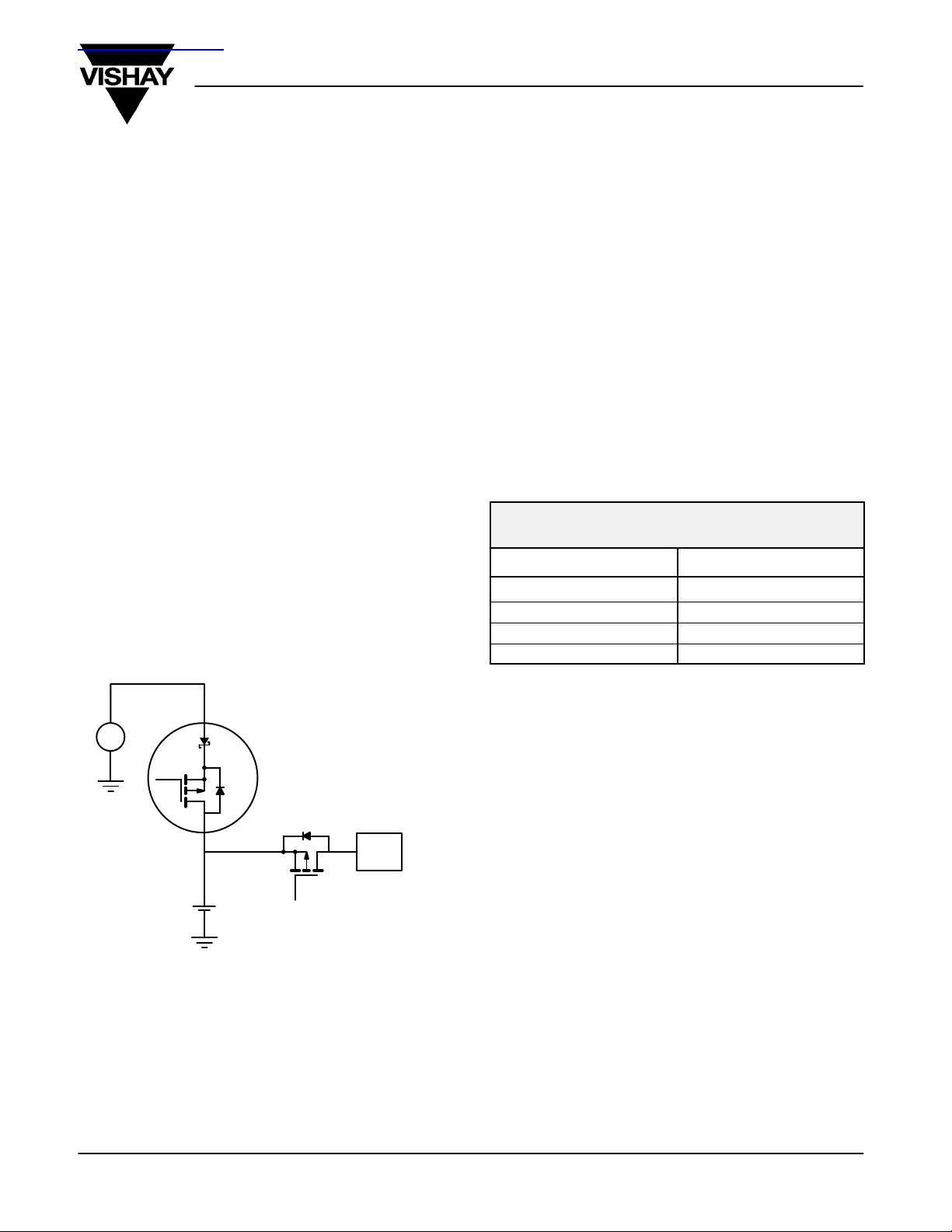
Charger
+
–
LITTLE FOOT Plust
To this end, moving away from a separate Schottky diode and
MOSFET to the single package integration of both devices, as
in the Vishay Siliconix LITTLE FOOT Plus
TM
, may have
significant advantages. However, in an integrated package
both components operate in a highly dissipative manner,
making the choice of package a critical decision.
The LITTLE FOOT Plus Schottky diodes come in a variety of
packages, with a range of r
the performance of the charger as r
values. Just as important to
DS(on)
values are the
DS(on)
thermal ratings of the packages. From the table below we can
see the choices of R
values available in today’s
thJA
industry-standard surface-mount packages.
TABLE 1.
LITTLE FOOT Plus PACKAGE OPTIONS
Device
SO-8 —Si4833DY 90
TSSOP-8 — Si6923DQ 115
TSOP-6 — Si3853DV 130
1206-8 ChipFET — Si5853DC 90
R
(_C/W) Typical
thJA
POWER DISSIPATION ISSUES
To select the correct part in the smallest package, the power
dissipated by the two power devices must be examined. In the
case of the charger switch, there are two modes of operation
to consider.
PA
Battery
FIGURE 1. LITTLE FOOT Plust Schottky—The Integrated
Solution of MOSFET and Schottky in One Power
Package
+
–
Regardless of the charging device selected, the designer is
still bound by space, cost, and efficiency considerations.
There is therefore an obvious desire to increase levels of
integration and reduce the component count and board size.
Document Number: 71395
22-Jan-01
In the first phase of charging, constant current is used and the
MOSFET is operated in the linear mode. In this mode the
device is effectively a variable resistor used to regulate the
battery charging current.
Once the battery has charged to the predetermined 4.1-V
level, the system voltage loop will begin to reduce the charging
current in order to maintain the desired float voltage, hence the
constant-voltage mode. For constant-voltage operation, the
controller will terminate the MOSFET linear operation and
revert to a pulse width modulation (PWM) mode. The
MOSFET is driven as a fully-saturated (Ohmic) switch.
The Schottky diode is always required in series with the switch
to prevent reverse current flow through the MOSFET’s body
drain diode when the external power source is unplugged or
unpowered. Using separate MOSFETs and Schottkys rather
than an integrated package consumes valuable board space.
www.vishay.com
1
Page 2
AN817
Vishay Siliconix
CONSTANTĆCURRENT MODE
As the MOSFET operates in the linear mode during
constant-current charge control, the device losses can be
simply calculated from Ohm’s law:
P
LOSS
= (V
BAT(max)
– V
BAT(min)
) x I
OUT
As an effective linear regulator, the MOSFET functions in a
high-dissipation mode. In addition, the series Schottky diode
contributes to the overall power loss. Typical charging currents
range from 400 mA to 700 mA, with the Li+ battery voltage
varying from 4.1 V (fully charged) to 3.0 V (discharged)
. So at
a 500-mA charging current, the charging system for a Li+ cell
will have to dissipate:
P
MOSFET = (4.1 * 3.0)=) 0.5 = 0.55 W
LOSS
P
Schottky = VF IF = 0.48 0.5 = 0.24 W
LOSS
In total, under constant current charging the total discrete
power loss = 0.79 W
CONSTANTĆVOLTAGE MODE
For the constant-voltage portion of the charge cycle, the
MOSFET is fully saturated. Any consequent losses will be
minimal and, assuming the worst-case scenario of T
and V
of 2.5 V, can be found from:
GS
PD Conduction = (Irms)2 r
P
Switching = 1/2 VL (tr + tf) FS W
D
= (0.5)
= 0.058 W
2
0.232
DS(on)
W
of 150°C
J
with 60°C as the benchmark. Therefore, to optimize the power
dissipation to the smallest MOSFET package the following
thermal equation can be used:
PD = (T
J(max)
– T
amb
)/R
thJA
Where:
PD = 0.79 W, T
Hence re-arranging for R
= 150_C and T
J(max)
= 114_C/W.
thJA
amb
= 60_C
Good engineering practice allows a safety margin of 10% on
the T
R
thJA
value, thus decreasing the allowable package
J(max)
to approximately 104°C/W.
From both the above calculation and Table 1, we can deduce
that the best-fit package for the MOSFET plus Schottky , while
still providing suitable power dissipation, are the SO-8
package and the recently introduced ChipFETt 1206
package.
However, moving upward in package footprint may not be an
option when heavily restrained by the device size. Therefore
the new ChipFET 1206 package offers a typical R
thJA
of only
90°C/W, a footprint 40% smaller than a TSOP-6, and a thermal
performance previously possible only with the SO-8 package.
TSOP-6
Assuming switching of 100 Hz
t
and a tf value of 1 ms.
r
0.5 (4.1 0.5) (1 10 * 6 + 1 10 * 6) 100 = 2 mW
Therefore, the losses generated from the MOSFET under
constant-voltage operation are much less—approximately
7.6% —than the losses generated under constant-current
operation.
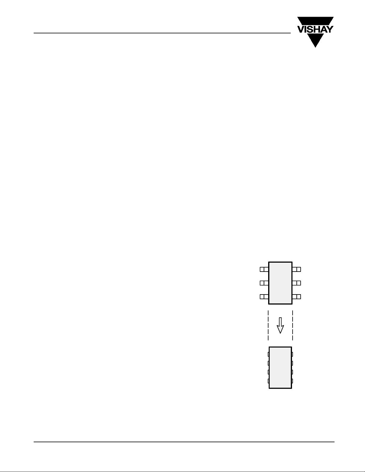
SMD PACKAGE THERMAL PERFORMANCE—
Can we dissipate the heat with LITTLE FOOT Plus?
Ambient temperatures usually quoted for component
calculation within a cell phone range between 50°C to 65°C,
www.vishay.com
2
40% Smaller Footprint
1206-8 ChipFET
FIGURE 2.
Document Number: 71395
22-Jan-01
Page 3

PACKAGE DIMENSIONS—1206Ć8 ChipFETt
AN817
Vishay Siliconix
4
D
6578
EE
4
1
3421
e
S b
2X 0.10/0.13 R
A
NOTES:
1 All dimensions are in millimeters
2 Mold gate burrs shall not exceed 0.13 mm per side.
Leadframe to molded body offset in horizontal and vertical shall not
3
exceed 0.08 mm.
4 Dimensions exclusive of mode gate burrs.
5 No mold flash allowed on the top and bottom lead surface.
ECN: S-59178—Rev. A, 17-Aug-99
L
5678
4321
c
Backside View
MILLIMETERS INCHES
Dim Min Nom Max Min Nom Max
A 1.00 – 1.10 0.039 – 0.043
b 0.25 0.30 0.35 0.010 0.012 0.014
c 0.1 0.15 0.20 0.004 0.006 0.008
D 2.95 3.05 3.10 0.116 0.120 0.122
E – – 1.80 – – 0.071
E
1.55 1.65 1.70 0.061 0.065 0.067
1
e 0.65BSC 0.0256BSC
L 0.30 – 0.45 0.012 – 0.018
S 0.55BSC 0.022BSC
5_Nom 5_Nom
Focusing on the Si5853DC, this device contains a 20-V
p-channel MOSFET—with a 160-mW r
value at a 2.5-V
DS(on)
gate drive—plus a 20-V, 1-A Schottky diode. From the
previous calculations, it can be seen that the Si5853DC can be
used as a constant-current/constant-voltage charging switch,
thus eliminating the use of two separate devices and saving
significant board space. From our working example, with a
500-mA charging current the die temperature is obtained from:
TJ = (T
TJ = (60_C 0.79) + 90_C/W
T
J
PD) + R
amb
= 137.4_C
thJA
This calculation proves that the Si5835DC is a satisfactory
solution for a typical constant-current/constant-voltage
charging strategy, and can effectively replace a separate
series connected MOSFET and Schottky diode, as is
commonly used within a cellular phone.
Document Number: 71395
22-Jan-01
2
Thermal Resistance Corroboration Between a 1-in
PCB
and a Cellular-Size PCA
The R
was based on the value measured on a 1-in
value—90°C/W— that was used in the calculations
thJA
2
PCB with 1-oz
copper on both sides, as is typically used for the
characterization of power MOSFET packages.
The subsequent characterization used a cellular-size PCA, so
using a point from this curve to compare thermal resistance
values—i.e., the 0.8-W point on the graph for 1206-8
ChipFET—then:
Q
= TJ – TA/P
JA
Q
= 98.5_C – 25_C/0.8
JA
Q
= 92_C/W
JA
D
The resulting QJA value is close to the 1-in2 PCB value of
90°C/W, adding credence to the earlier calculations.
www.vishay.com
3
Page 4

AN817
Vishay Siliconix
TEST RESULTS
The following graph displays the power dissipation
performance of the TSOP-6 vs. the 1206-8 on a cellular-size
PCA.
The TSOP-6 package has been used to compare performance
due to its status as the preferred footprint for power MOSFET s
in cellular designs.
Incremental steps of power were dissipated in each device
and the corresponding junction temperature was measured.
The 1206-8 ChipFET has superior P
reference points, i.e., T
= 100_C (TA of 25_C is included in
J
this value).
140
TSOP-6 = 690 mW
120
C)
_
Junction T emperature (
1206-8 ChipFET = 805 mW
100
80
60
40
20
0
0.0 0.2 0.4 0.6 0.8 1.0
TSOP-6
performance at all
D
1206-8 ChipFET
APPENDIX A
A Typical Charging Scheme
The world market for high-density rechargeable batteries as a
whole is in a transition phase between market development
and market maturation. The four most common chemistries
used to power portable equipment are Nickel Cadmium
(NiCd), Nickel Metal Hydride (NiMH), Lithium Ion (Li+) and
Lithium Polymer (LiP). NiCd is currently in market retirement,
NiMH is in full maturation, Li+ is in the market development
stage and new alternatives like LiP are in market gestation. For
today’s cellular phone, a single-cell Li+ cell is often the battery
of choice due to its small size and high energy density.
Li+ cells are generally suited to a
constant-current/constant-voltage charging strategy and
although relatively simple to implement, charging the cell
actually requires precise control of the “float voltage” region in
order to obtain the maximum capacity with long cell life. In
summary, if the voltage is too low, the cell will not be fully
charged; if the voltage is too high, the cycle life is significantly
degraded. In addition, excessive over- or under-charge of a
Li+ cell can result in catastrophic failure of the unit with
possible explosion.
As stated, the charging of a single Li+ cell will follow a CC/CV
strategy, as shown in the graph below. Region 1 is CC,
region 2 is CV.
Device Power Dissipation
FIGURE 3. Comparison of TSOP-6 vs. ChipFET
Both examples (practical and theoretical) demonstrate the
validity of using the LITTLE FOOT Plus MOSFET and
Schottky integration power package.
The Si5853DC has been shown to be a viable application for
the charger switch in single lithium-ion charging schemes.
ASSOCIATED MATERIAL
1. Design Challenges for Battery Operated Power
Management Systems: Guy Moxey, Vishay Siliconix,
PCIM2000 Europe.
2. Leadless Power Packaging Signals a New Era for Surface
Mount Semiconductor Switches: Guy Moxey,
Vishay Siliconix, Electronic Engineering, June 2000 Issue.
3. Single-Channel 1206-8 ChipFETt Power MOSFET
Recommended Pad Pattern and Thermal Performance:
Michael Speed, V ishay Siliconix: TA811, www.vishay.com
A fully discharged cell (typically 3 V) will initially be charged by
a constant current, since the cell’s voltage is well below the
4.1-V constant voltage limit. Once the cell’s voltage rises to the
float voltage of 4.1 V, the charging circuitry limits the further
rise in terminal voltage and the charging current naturally
begins to decline. Typically, manufacturers recommend that
the charging sequence be terminated roughly one hour after
the current has fallen to 10% of its peak value.
.
www.vishay.com
4
Document Number: 71395
22-Jan-01
Page 5

AN817
Vishay Siliconix
4.5
4.0
3.5
3.0
2.5
2.0
Cell Voltage (V)
1.5
1.0
0.5
0.0
0.0 0.5 1.0 1.5 2.0 2.5 3.0 3.5 4.0
Cell Voltage
1 2
Charging Current
Charge Time (Hrs)
FIGURE 4.
4.1 V
Document Number: 71395
22-Jan-01
www.vishay.com
5
 Loading...