

Page 1
查询AN804供应商
Vishay Siliconix
P-Channel MOSFETs, the Best Choice for High-Side Switching
AN804
Historically, p-channel FETs were not considered as useful as
their n-channel counterparts. The higher resistivity of p-type
silicon, resulting from its lower carrier mobility, put it at a
disadvantage compared to n-type silicon.
Getting n-type performance out of p-type FETs has meant
larger area geometries with correspondingly higher
inter-electrode capacitances. Consequently, a truly
complementary pair—a p-channel and an n-channel device
that match in
all
parameters—is impossible.
Yet, despite its shortcomings, the p-channel MOSFET
performs a vital “high-side” switch task that the n-channel
simply cannot equal.
Used as a high-side switch, a p-channel MOSFET in a
totem-pole arrangement with an n-channel MOSFET will
simulate a high-current, high-power CMOS (complementary
MOS) arrangement. Although the p-channel MOSFET cannot
complement the n-channel in both on-resistance and
capacitance simultaneously, such combinations as the
low-threshold p-channel TP0610 and the n-channel 2N7000
together offer outstanding performance as a complementary
pair.
Switching Ground-Return Loads
The principal application of the p-channel, enhancementmode MOSPOWER FET is in switching power (or voltage) to
grounded (ground return) loads.
T o drive the FET properly , the gate voltage must be referenced
to its source. For enhancement-mode MOSFETs, this gate
potential is of the same polarity as the MOSFET’s drain
voltage. T o turn on, the n-channel MOSFET requires a positive
gate-source voltage, whereas the p-channel MOSFET
requires a negative gate-source potential.
During switching, a MOSFET’s source voltage must remain
fixed, as any variation will modulate the gate and thus
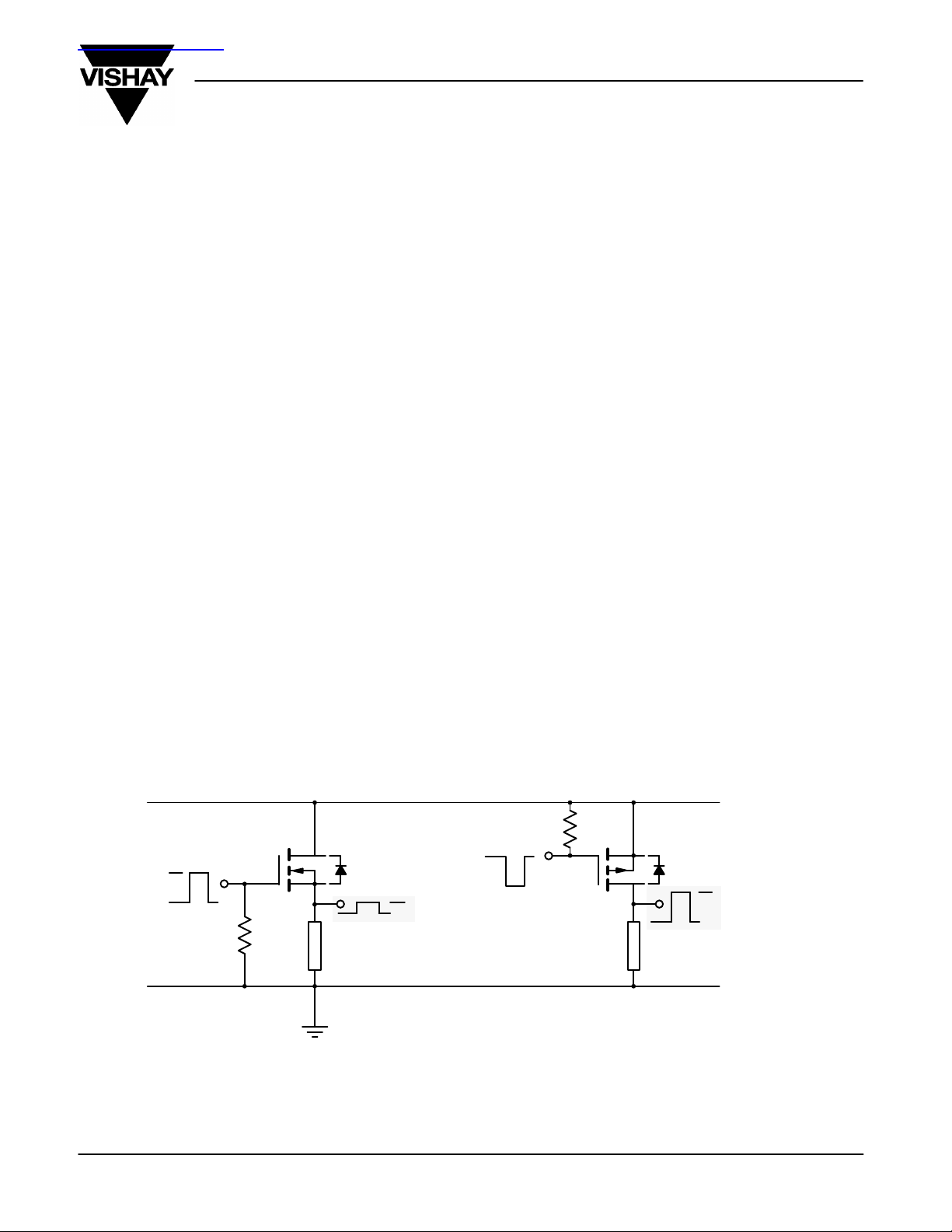
adversely affect performance. Figure 1 shows this
degradation by comparing n-channel and p-channel MOSFET
high-side switching.
V
GG
0
FIGURE 1. Comparing the Performance Between N-Channel and P-Channel Grounded-Load Switching
Document Number: 70611
10-Mar-97
P-ChannelN-Channel
V
DD
VGG – V
0
Load
(1a) (1b)
th
V
DD
VDD – ILr
DS
0
Load
www.vishay.com FaxBack 408-970-5600
1
Page 2
AN804
Vishay Siliconix
If an n-channel, enhancement-mode MOSFET were switching
a positive-polarity voltage to a grounded load, the output would
be limited to V
GG
– Vth.
The equations describing performance of the n-channel
ground-switching MOSFET with a ground-reference gate drive
are based on the relationship between V
≥ VGG, then VO = VGG – V
If V
DD
If V
< VGG – V
DD
th
. then VO = VDD – ILr
;
th
and VGG:
DD
DS(on)
.
Sustaining a more acceptable gain with an output in direct
relation to V
would require an isolated gate drive referenced
DD
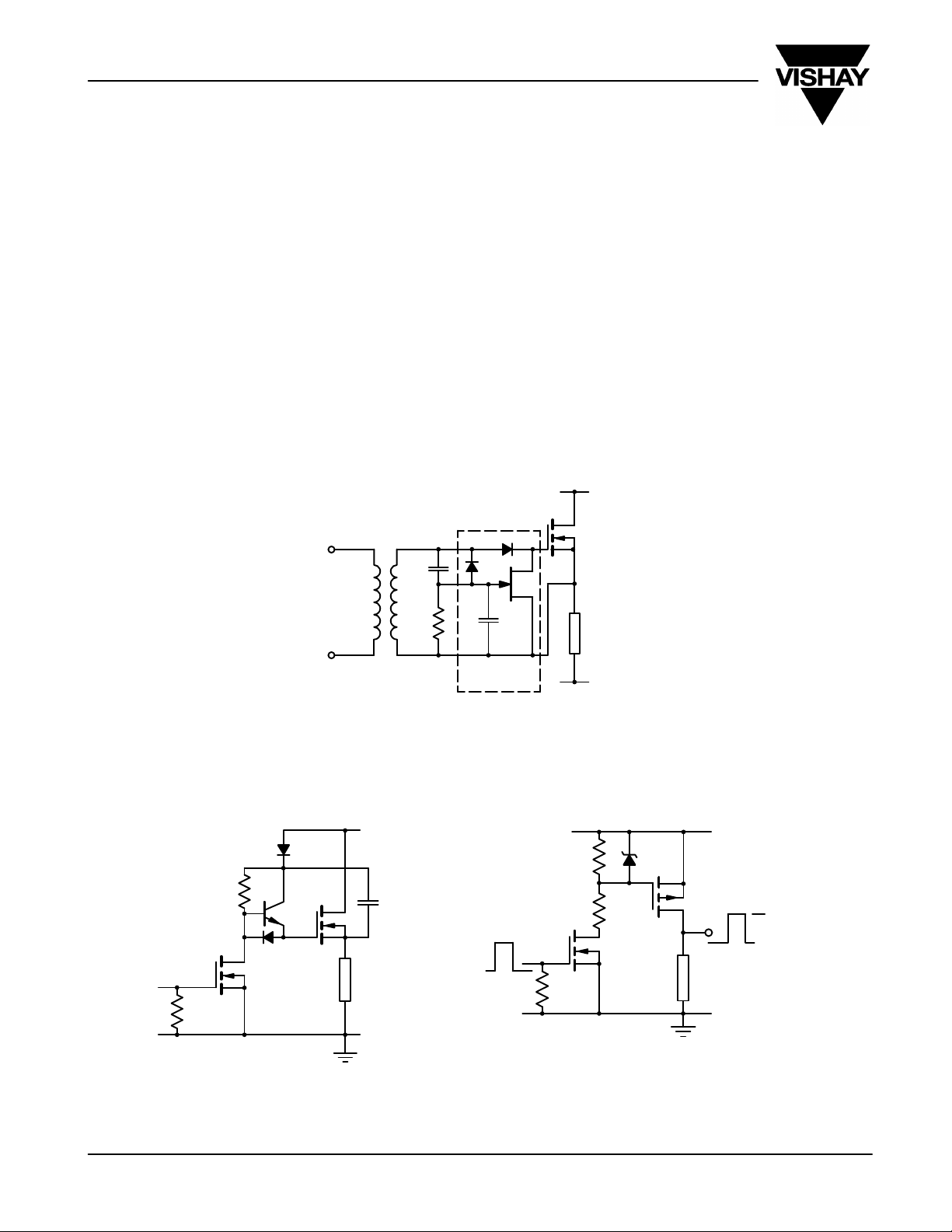
to the source (Figure 4). The dc bias option rectifies the pulse
of ac from the transformer and stores a “+” voltage on the
A
gate-to-source capacitance of the MOSFET. The RC
determines the turn off time.
Bootstrapping the n-channel MOSFET (Figure 2) is
satisfactory for short turn-on times of a few milliseconds. In this
arrangement, both MOSFETs must have breakdown voltage
specifications that match or exceed the supply voltage.
Using a p-channel MOSFET may place some severe
restraints on the gate drive, since the gate must be close to
V
(Figure 1b). To return gate control to a more acceptable
DD
logic format, add an n-channel MOSFET (Figure 3).
Using an n-channel MOSFET in this way simplifies the gate
drive for a high-voltage, high-side, p-channel MOSFET.
Placing a Zener diode between the gate and supply ensures
that V
(BR)GSS
will not be exceeded. Again, both MOSFETs
must withstand the full rail voltage.
TTL
N-Channel
RC
B
FIGURE 4. Floating Gate Drive
V
DD
N-Channel
dc Bias
Options
TTL
Load
15 V
N-Channel
V
DD
P-Channel
Load
VDD – ILr
DS
FIGURE 2. Bootstrapping for N-Channel
Grounded-Load Switching
www.vishay.com FaxBack 408-970-5600
2
FIGURE 3. Using An N-Channel Level-Shifter
Simplifies Driving From Logic
Document Number: 70611
10-Mar-97
Page 3
AN804
Vishay Siliconix
Half-Bridge (T otem Pole)
A high-side p-channel MOSFET and a low-side n-channel
MOSFET tied with common drains (Figure 5) make a superb
high-current “CMOS equivalent” switch. One fault common to
such circuits has been the excessive crossover current during
switching that may occur if the gate drive allows both
MOSFETs to be on simultaneously .
+V
DD
+15 V
P-Channel
+15 V
V
OUT
–15 V
N-Channel
I
DD
FIGURE 5. Low-Voltage Complementary
MOSPOWER Array
–V
–15 V
DD
Properly driving the MOSFET gates can minimize unwanted
crossover current at high supply voltages (both +V
and –VDD)
DD
(Figure 6).
A resistively-coupled lower-power complementary pair
offers extremely low crossover current when the output stage
uses high-power MOSFET s. The Zener, Z1, and resistors, R1
and R3, act as a level shifter, properly driving the low-power
MOSFETs. The Zener may be selected according to the
equation
V
where +V
ZENER
= 2 VDD – V
= –V
DD
DD
th
Whatever crossover current that might occur in the low-power
drivers is dramatically reduced by the series resistor, R4.
Additionally , driving the high-power complementary pair using
this resistor divider scheme all but eliminates crossover
current in this critical output driver. This increases both the
driver’s efficiency and its reliability.
TABLE 1. NĆ AND PĆCHANNEL DUAL
MOSFETS IN SOĆ8 PACKAGE
FOR OUTPUT STAGE
Part
Number
Si9939DY 30/–30 0.05/0.1 3.5/–3.5
Si9942DY 20/–20 0.125/0.2 3/–2.5
Si9928DY 20/–20 0.05/0.11 5/–3.4
V
(BR)DSS
(V) rDS Max () ID (A)
R1
R2
N-Channel
TTL
FIGURE 6. High-Voltage Complementary Pair Driven by Logic-Compatible MOSFET
Z1
R3
R4
+V
P-Channel
N-Channel
–V
DD
DD
Document Number: 70611
10-Mar-97
www.vishay.com FaxBack 408-970-5600
3
Page 4
AN804
Vishay Siliconix
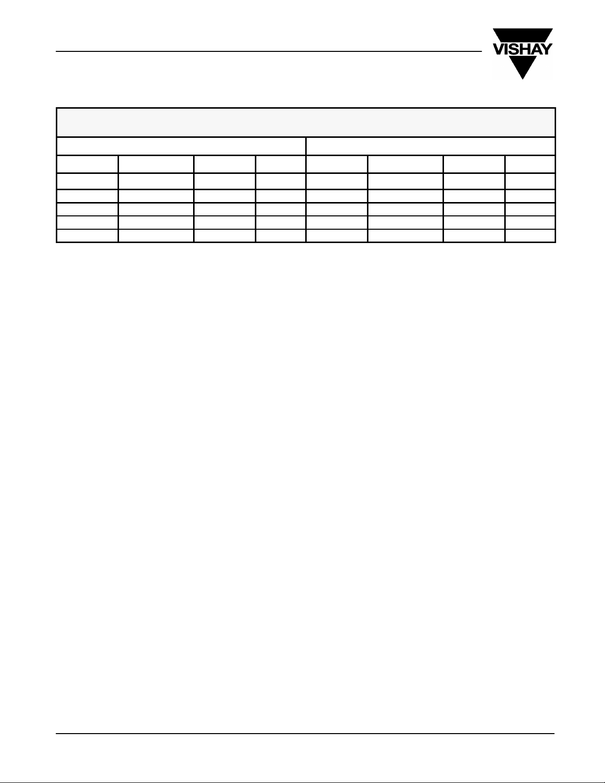
T ABLE 2. POPULAR DISCRETE NĆ AND PĆCHANNEL MOSFETS FOR INPUT DRIVER ST AGES
AND OUTPUTS
P-Channel Devices N-Channel Devices
Part Number V
VP0300L –30 2.5 TO-226AA VN0300L 30 1.2 TO-226AA
TP0610L –60 10 TO-226AA 2N7000 60 5 TO-226AA
VP2020L –200 20 TO-226AA VN2010L 200 10 TO-226AA
TP0101T* –12 0.65 TO-236 TN0200T* 20 0.4 TO-236
TP0610T* –60 10 TO-236 2N7002* 60 7.5 TO-236
*Surface Mount Package
(BR)DSS
Min (V) rDS Max () Package Part Number V
(BR)DSS
Min (V) rDS Max () Package
www.vishay.com FaxBack 408-970-5600
4
Document Number: 70611
10-Mar-97
 Loading...