

Kandarp Pandya
INTRODUCTION
AN606
Vishay Siliconix
Current-Sensing Power MOSFETs
Vishay Siliconix current-sensing power MOSFETs offer a
simple means of incorporating a protection feature into an
electronic control circuit and avoiding catastrophic failures
resulting from overcurrent (overload) and/or short-circuit
conditions. The device package is a modified D2PAK with five
pins. The MOSFET termination retains the standard D
2
PAK
footprint for a three-pin device. The additional two pins provide
termination for a current-sense output and an internal Kelvin
connection to the source. For current sensing, the MOSFET
design employs a small number of the total number of
MOSFET cells in a known ratio. The latter define the
current-sense parameters. A typical control interface uses a
simple circuit with an op-amp or a comparator. This approach
offers the freedom of control-level setting and facilitates its
incorporation into the main control system.
DEVICE DESCRIPTION AND PRINCIPLE OF
OPERATION
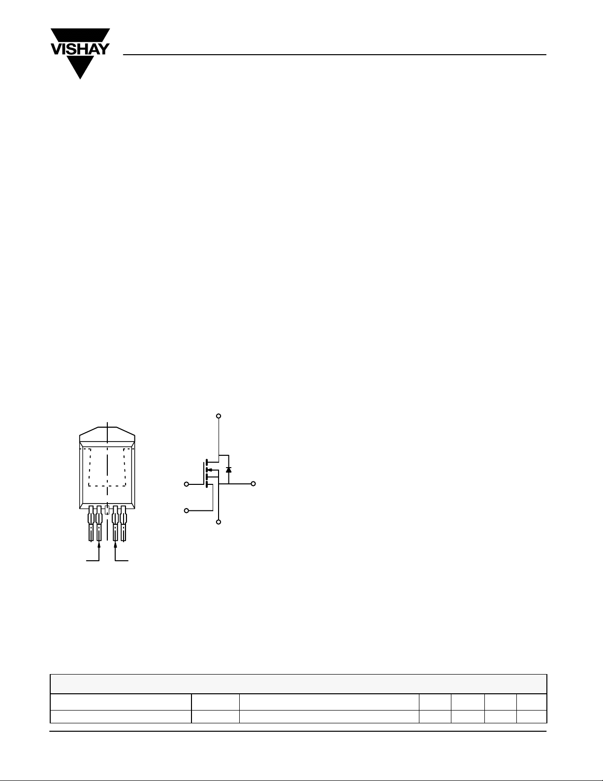
D2PAK-5
D (Tab, 3)
between gate and drain-stub and between drain-stub and source,
respectively. See Application Note 826, Recommended Minimum
Pad Patterns With Outline Access for Vishay Siliconix
MOSFETs (http://www.vishay.com/doc?72286), for the
recommended PCB layout dimensional details of the pad pattern.
Modified-part library symbols for schematic symbol and PCB
layout are available on the “Protel” (PCB design software)
platform. For soft copy, please contact Vishay Siliconix in Santa
Clara, Calif., in the United States, by phoning 1-408-567-8927.
The Principle Behind the Current-Sensing Feature
The most efficient way to sense the drain-source current is to
use the ratio-metric measurement. In a power MOSFET, it is
possible to implement this method easily.
The cell density, a favored term within the power MOSFET
industry, conveys that the power MOSFET structure consists
of many cells connected in parallel. In principle, these cells
constitute a resistive path for drain-source current. Electrically,
these cells are parallel connected resistors, r
DS(on)
s. Each cell
- being identical in structure and electrical characteristics shares the current equally when the device is on. This property
enables design of a MOSFET with a current-sensing feature.
(1)
G
324
51
SENSE
SENSE
FIGURE 1. Package Information and Schematic Symbol
SGD
KELVIN
(2)
N-Channel MOSFET
S (5)
(4)
KELVIN
Package Information and Schematic Symbol, Figure 1, shows a
partial reproduction of a datasheet for a current-sensing
MOSFET, SUM50N03-13C. Gate, drain-stub/tab, and source
(pins 1, 2, and 3) are in the same position as in a standard D
2
PAK
(TO-263) MOSFET. However, pin-out modification is required to
incorporate current-sense (pin 2) and Kelvin-to-source (pin 4)
TABLE 1: Current Sense Characteristics
Current Sensing Ratio r ID = 1 A, V
Mirror Active Resistance r
Document Number: 71991
17-Dec-03
m(on)
Dividing the MOSFET cells in a known ratio creates two paths
that share the drain-source current. The path with the smaller
number of cells constitutes the sense current, which is much
smaller than the current conducting through the rest of the
cells. A very simple, low-power, external circuit can measure
this current. Multiplying this value with the cell ratio gives the
total drain-source current.
The classic Kelvin termination for the return of sense current
to the main source connection insures the measurement
accuracy. This terminal not only eliminates the ground loop,
but also minimizes the imbalance of internal structures with
two current paths.
The Current-Sensing Parameters, Table 1, and the
Current-Sense Die Characteristics and Schematic, Figure 2,
help to demonstrate the current-sensing operation and circuit
implementation.
= 10 V, R
GSS
VGS = 10 V, ID = 10 mA 3.5 W
= 1.1 W 420 520 620
SENSE
www.vishay.com
1
AN606
Vishay Siliconix
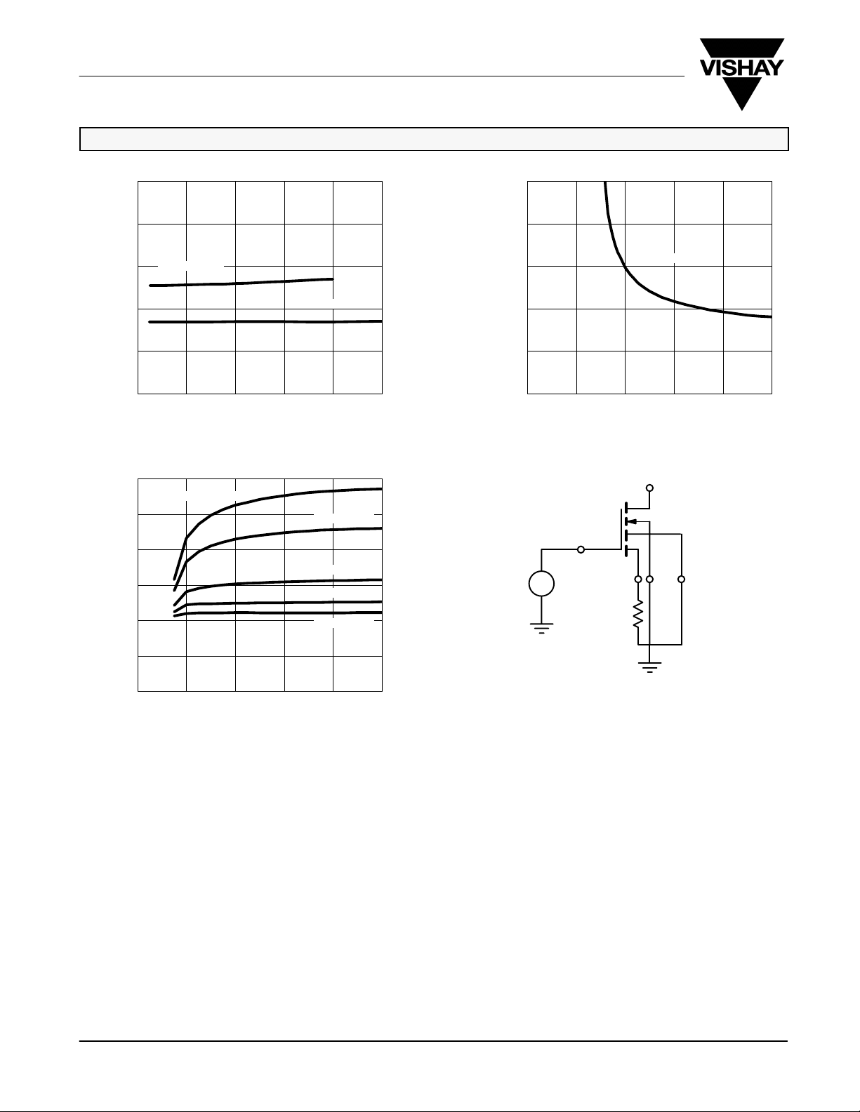
TYPICAL CHARACTERISTICS (25_C UNLESS NOTED) SENSE DIE
10
8
6
4
− On-Resistance (W)
m(on)
r
2
0
0.00 0.02 0.04 0.06 0.08 0.10
1200
1000
800
600
Ratio
400
On-Resistance vs. Sense Current
VGS = 4.5 V
I
(A)
SENSE
Current Ratio (I
vs. Gate-Source Voltage (Figure 1)
RS = 6.6 W
(MAIN)/IS
VGS = 10 V
)
RS = 4.7 W
RS = 2.2 W
RS = 1.1 W
RS = 0.5 W
On-Resistance vs. Gate-Source Voltage
10
8
6
4
− On-Resistance (W)
m(on)
r
2
0
0246810
− Gate-to-Source Voltage (V)
V
GS
G
SENSE S KELVIN
V
G
R
ID = 10 mA
S
200
0
048121620
VGS − Gate-to-Source Voltage (V)
FIGURE 2. Current-Sensing Die Characteristics and Schematic
Definition of Current-Sensing Parameters
The current-sense ratio, r, is the quotient of the number of cells
terminated on the sense terminal to the total number of cells on
the MOSFET die.
To derive the value of r using the above definition requires
detailed die design. However, the quotient of drain current to
the sense current provides the same value because these
current values are the sum of cell current in each path.
Mathematically:
r = I
D/ISENSE
ID is drain current
www.vishay.com
2
I
is the current flowing out of the sense terminal and into
SENSE
the sense resistor, R
Mirror active resistance, r
SENSE
, is the resistance of parallel
m(on)
connected cells used in the sense chain when the device is on.
Being r
as in any other MOSFET, the value depends on
DS(on)
the gate drive, drain current, and junction temperature.
Accordingly, r
is defined at given values of VGS, I
m(on)
DRAIN
and TJ junction.
By definition, for the sense die, refer to Figure 2. Mirror active
resistance r
at 4.5 V and 10 V, corresponding drain-source current I
up to 0.1 A, and junction temperature TJ at 25
temperature coefficient of r
is specified at the gate-source voltages, V
m(on)
is the same as that of r
m(on)
SENSE
_
C. The
DS(on)
GS
Refer to the on-resistance vs. junction temperature curve in
Figure 3.
Document Number: 71991
17-Dec-03
,
.

AN606
Vishay Siliconix
On-Resistance vs. Junction Temperature
2.0
V
= 10 V
GS
I
1.8
1.6
1.4
Normalized
1.2
− On-Resistance (W)
m(on)
1.0
r
0.8
0.6
= 25 A
D
−50 −25 0 25 50 75 100 125 150 175
T
− Junction Temperature (_C)
J
FIGURE 3. Normalized r
for the Sense Die
m(on)
DESIGN EQUATIONS
The following three equations enable circuit design and
analysis.
= x ID/r
I
SENSE
VDS = I
V
= ID x r
DS
V
SENSE
V
SENSE
x [r
SENSE
DS(on)
= I
SENSE
= VDS x R
m(on)
/(r
m(on)
x R
SENSE
+ R
+ R
SENSE
/(r
SENSE
SENSE
or
m(on)
] or
+ R
)
SENSE
)
2. use a minimum value of the I
signal at the maximum
SENSE
value of ID; and
3. use a fast comparator with hysterisis to control and protect
the MOSFET.
Typical schematic configurations for implementing the current
sense are shown in Figure 4 and Figure 5.
The Virtual Earth Sensing Scheme, Figure 4, is suitable for
applications aiming at higher noise immunity and speed. This
approach also improves measurement accuracy by
eliminating the sense resistor. However, a dual power supply
and inverted (negative) output signal are the price designers
pay for deriving these benefits.
The Resistor Sensing Scheme shown in Figure 5 is a quite
simple and economical approach. The accuracy of current
measurement is affected by the introduction of an external
sense resistor RS. However, the latter aids in lowering the
temperature sensitivity of the current-sense signal.
V
DD
Load
I
L
D
Kelvin
G
+V
Sense
−
+
V
1
Where I
SENSE
Current flowing out of sense terminal
r Current-sensing ratio
I
Drain-source current
D
V
DS
r
m(on)
R
SENSE
Drain-source voltage
Mirror active resistance
External current-sense resistor
Application Aspects and Design Examples
The current-sense ratio r, even though fixed by design, is
dependent on manufacturing process variations.
Furthermore, mirror active resistance r
parameters V
and ID and junction temperature TJ. As a
GS
depends on circuit
m(on)
result, a practical design can realize an accuracy of 15% —
20% for current sensing. Accordingly, the current-sensing
MOSFET is most suitable for supervisory functions such as
overcurrent and/or short-circuit protection.
Three keys to a successful design are to:
1. have an adequate margin between the normal
operating-current value and the trip-current value;
Document Number: 71991
17-Dec-03
−V
S
FIGURE 4. Virtual Earth Sensing Scheme
V
DD
Load
I
L
D
R3
Kelvin
G
R1
Sense
S
Stray
Resistance
R2
−
+
V
1
FIGURE 5. Resistor Sensing Scheme
www.vishay.com
3

AN606
D2PAK
Vishay Siliconix
Part # Channel Type VDS (VDC) rDS (W) IDS (A) PD (W) Package
TABLE 2: Current Product Range
Si6862DQ
Si4730EY
SUM50N03-13LC
SUM60N08-07C
N 20 0.026/4.5 V 6.6 1.8 TSSOP-8*
N 30 0.015/10 V 11.7 3.6 SO-8*
N 30 0.013/10 V 50 83
N 75 0.007/10 V 60 300
2
-
-5
Recommended minimum pads for current-sensing MOSFETs in TSSOP-8 and SOIC-8 packages see application note AN826
(http://www.vishay.com/doc?72286).
CONCLUSION
Vishay Siliconix current-sensing power MOSFETs enable
implementation of a simple solution for incorporating
supervisory protection features such as overcurrent and/or
short circuit. This approach offers the freedom and flexibility of
control-circuit design, though the accuracy of measurement is
not suitable for current-control applications. Virtually any
power MOSFET from the Vishay Siliconix product range can
be supplied with a current-sensing feature.
www.vishay.com
4
Document Number: 71991
17-Dec-03
 Loading...