

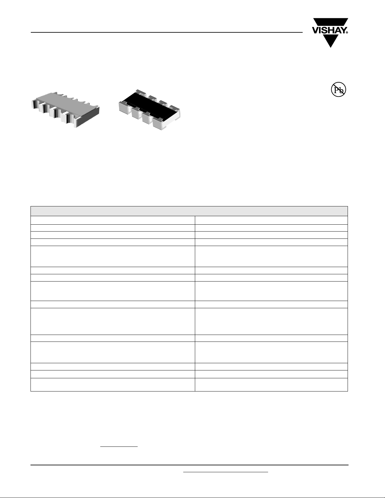
ACAC 0612, ACAS 0612 - Precision
Vishay Beyschlag
Precision Thin Film Chip Resistor Array
ACAC 0612 (concave terminations) and ACAS 0612 (convex
terminations) thin chip resistor arrays combine the proven
reliability of precision thin film chip resistor products with the
advantages of chip resistor arrays. Defined tolerance
matching and TCR tracking makes this product perfectly
suited for applications with outstanding requirements
towards stable fixed resistor ratios. A small package enables
the design of high density circuits in combination with
reduction of assembly costs. Four equal resistor values or
two pairs are available.
FEATURES
•
Advanced thin film technology
• Two pairs or four equal resistor values
• TCR tracking down to 10 ppm/K (± 5 ppm/K)
RoHS
COMPLIANT
• Tolerance matching down to 0.1 % (± 0.05 %)
• Pure Sn termination on Ni barrier layer
•
RoHS compliant component, compatible with lead (Pb)-free
and lead containing soldering processes
APPLICATIONS
• Precision analogue circuits
• Voltage divider
• Feedback circuits
• Signal conditioning
TECHNICAL SPECIFICATIONS
DESCRIPTION ACAC 0612, ACAS 0612
EIA size 0612
Metric size RR1632M
Configuration, isolated 4 x 0603
Design:
All Equal AE
Two Pairs TP
Resistance values 47 Ω to 221 kΩ
Absolute tolerance ± 0.5 %; ± 0.25 %
Tolerance matching
Absolute temperature coefficient ± 50 ppm/K; ± 25 ppm/K
Temperature coefficient tracking
Max. resistance ratio R
Rated dissipation: P
Element 0.1 W
Package, 4 x 0603 0.3 W
Operating voltage 75 V
Film temperature 125 °C
Insulation voltage (U
resistors, continuous
Notes
(1)
Resistance values to be selected from E24, E48 and E96
(2)
Higher resistance ratio is available on request
(3)
The power dissipation on the resistor generates a temperature rise against the local ambient, depending on the heat-flow support of the printed
circuit board (thermal resistance). The rated dissipation applies only if the permitted film temperature is not exceeded. Furthermore, a high
level of ambient temperature or of power dissipation may raise the temperature of the solder joint, hence special solder alloys or board
materials may be required to maintain the reliability of the assembly.
(4)
For higher max. film temperature and AEC-Q200 qualification please refer to data sheet “Automotive Precision Thin Film Chip Resistor Array“
available on our web site at www.vishay.com
• These resistors do not feature a limited lifetime when operated within the permissible limits. However, resistance value drift increasing over
operating time may result in exceeding a limit acceptable to the specific application, thereby establishing a functional lifetime.
www.vishay.com For technical questions, contact: filmresistors.thinfilmarray@vishay.com
276 Revision: 12-Mar-08
min./Rmax.
(3)
70
) against ambient and between isolated
ins
0.5 % (equivalent to ± 0.25 %)
0.25 % (equivalent to ± 0.125 %)
0.1 % (equivalent to ± 0.05 %)
50 ppm/K (equivalent to ± 25 ppm/K)
25 ppm/K (equivalent to ± 12.5 ppm/K)
15 ppm/K (equivalent to ± 7.5 ppm/K)
10 ppm/K (equivalent to ± 5 ppm/K)
1:5
75 V
(1)
(2)
(4)
Document Number: 28751
ACAC 0612, ACAS 0612 - Precision
Precision Thin Film Chip Resistor Array
PART NUMBER AND PRODUCT DESCRIPTION
(1)
Vishay Beyschlag
PART NUMBER: ACASA1100A2200P500
SA1100A 2 0C AA 20 50P0
MODEL TERMINAL SIZE
ACA C = Concave
A = 0612
S = Convex
RESISTANCE
(2) (3)
VAL UE
3 digit
resistance
value R1, R4
1 digit multiplier
MULTIPLIER
9 = *10
0 = *10
1 = *10
2 = *10
3 = *10
-1
0
1
2
3
PRODUCT DESCRIPTION: ACAS 0612 110R A 220R P5
ACA S 0612 110R A 220R P5
MODEL
ACA = Chip
Array
TERMINATION
C = Concave
S = Convex
SIZE
0612 110R = 110 Ω
Notes
(1)
Products can be ordered using either the PART NUMBER or the PRODUCT DESCRIPTION
(2)
Please refer to APPLICATION INFORMATION, see below
(3)
Different resistance values are available on request
(4)
Please refer to table TEMPERATURE COEFFICIENT AND RESISTANCE RANGE, see below
(5)
Please refer to table PACKAGING, see below
ACCURACY
GRADE
TCR, Tracking,
Tolerance and
Matching
A, B, E, F,
J, K, N or P
RESISTANCE
VALUE R1, R4
1K1 = 1.1 kΩ
22K1 = 22.1 kΩ
(4)
(2) (3)
RESISTANCE
(2) (3)
VAL UE
3 digit
resistance
value R2, R3
1 digit multiplier
MULTIPLIER
9 = *10
0 = *10
1 = *10
2 = *10
3 = *10
-1
0
1
2
3
ACCURACY
(4)
GRADE
TCR, Tracking,
Tolerance and
Matching
A, B, E, F,
J, K, N or P
PA CK A G I NG
P1
P5
PW
RESISTANCE
VAL U E R 2 , R 3
220R = 220 Ω
1K1 = 1.1 kΩ
22K1 = 22.1 kΩ
(2) (3)
(5)
PACKAGING
SPECIAL
00
= Standard
P1
P5
PW
(5)
PACKAGING
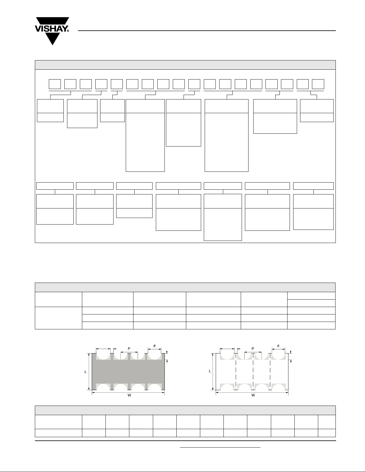
MODEL TAPE WIDTH DIAMETER PIECES PITCH
ACAC 0612
ACAS 0612
8 mm 180 mm/7" 1000 4 mm P1
8 mm 180 mm/7" 5000 4 mm P5
8 mm 330 mm/13" 10 000 4 mm PW
PACKAGING CODE
PAPER TAPE
DIMENSIONS ACAC 0612 in millimeters
W
I
T
1
T
1
Top view Bottom view
W
I
T
2
T
2
DIMENSIONS - chip resistor array, mass and relevant physical dimensions
TYPE
L
(mm)W(mm)
ACAC 0612 1.6 ± 0.15 3.2 ± 0.15 0.55 ± 0.1 0.8 ± 0.1 0.5 ± 0.15 0.3 ± 0.15 0.4 ± 0.15 0.3 ± 0.1 min. 0.15 min. 0.25 9.41
Document Number: 28751 For technical questions, contact: filmresistors.thinfilmarray@vishay.com
Revision: 12-Mar-08 277
H
(mm)
P
(mm)
W
(mm)
T
T
1
(mm)
T
2
(mm)d(mm)
l
1
(mm)
l
2
(mm)
MASS
(mg)
www.vishay.com

ACAC 0612, ACAS 0612 - Precision
Vishay Beyschlag
Precision Thin Film Chip Resistor Array
DIMENSIONS ACAS 0612 in millimeters
A
T
2
T
1
H
A
1
A
DIMENSIONS - chip resistor array, mass and relevant physical dimensions
TYPE
W
(mm)
ACAS 0612 1.5 ± 0.15 3.2 ± 0.15 0.45 ± 0.1 0.8 ± 0.1 0.6 ± 0.15 0.4 ± 0.15 0.3 ± 0.15 0.4 ± 0.15 9.41
L
(mm)
H
(mm)
P
(mm)
A
1
(mm)
A
(mm)
T
1
(mm)
T
2
(mm)
PATTERN STYLES FOR CHIP RESISTOR ARRAYS
ACAS 0612
UI X
Y
G
Z
Dimensions in mm
limits for solder resistance
0.1
ACAC 0 612
Z
G
Y
MASS
(mg)
X
P
I
P
0.1
RECOMMENDED SOLDER PAD DIMENSIONS FOR CHIP RESISTOR ARRAYS
TYPE
G
(mm)
ACAC 0612 0.7 0.7 0.5 - 2.1 0.3 0.8
ACAS 0612 0.8 1.15 0.63 0.44 3.1 0.36 0.8
Y
(mm)
X
(mm)
U
(mm)
Z
(mm)
I
(mm)
(mm)
TEMPERATURE COEFFICIENT AND RESISTANCE RANGE
DESCRIPTION RESISTANCE VALUE
ACCURACY
GRADE
ABSOLUTE TCR
(1)
TCR TRACKING
ABSOLUTE
TOLERANCE
(1)
A ± 25 ppm/K 10 ppm/K ± 0.25 % 0.1 % 47 Ω to 221 kΩ
B ± 25 ppm/K 10 ppm/K ± 0.5 % 0.25 % 47 Ω to 221 kΩ
E ± 25 ppm/K 15 ppm/K ± 0.25 % 0.1 % 47 Ω to 221 kΩ
F ± 25 ppm/K 15 ppm/K ± 0.5 % 0.25 % 47 Ω to 221 kΩ
J ± 25 ppm/K 25 ppm/K ± 0.25 % 0.1 % 47 Ω to 221 kΩ
K ± 25 ppm/K 25 ppm/K ± 0.5 % 0.25 % 47 Ω to 221 kΩ
N ± 50 ppm/K 25 ppm/K ± 0.5 % 0.5 % 47 Ω to 221 kΩ
P ± 50 ppm/K 50 ppm/K ± 0.5 % 0.5 % 47 Ω to 221 kΩ
Note
(1)
In applications with defined resistance ratios like voltage dividers or feedback circuits, an array with a defined tracking of e.g. 10 ppm/K is
required to replace discrete resistors with a temperature coefficient of ± 5 ppm/K. Furthermore, in order to achieve the same tolerance of
± 0.05 % of individual resistors, an array requires a matching of 0.1 %.
TOLERANCE
MATCHING
ACAC 0612, ACAS 0612
P
www.vishay.com For technical questions, contact: filmresistors.thinfilmarray@vishay.com Document Number: 28751
278 Revision: 12-Mar-08

ACAC 0612, ACAS 0612 - Precision
Precision Thin Film Chip Resistor Array
APPLICATION INFORMATION
R
1
DESCRIPTION
The production of the components is strictly controlled and
follows an extensive set of instructions established for
reproducibility. A homogeneous film of metal alloy is
deposited on a high grade (96 % Al
and conditioned to achieve the desired temperature
coefficient. Specially designed inner contacts are realised on
both sides. A special laser is used to achieve the target value
by smoothly cutting a meander groove in the resistive layer
without damaging the ceramics.
The resistor elements are covered by a protective coating
designed for electrical, mechanical and climatic protection.
The terminations receive a final pure tin on nickel plating.
The result of the determined production is verified by an
extensive testing procedure and optical inspection
performed on 100 % of the individual chip resistors. Only
accepted products are laid directly into the paper tape in
accordance with IEC 60286-3*.
R
2
Circuit Type 03
R
3
2O3
R
4
) ceramic substrate
Vishay Beyschlag
ASSEMBLY
The resistors are suitable for processing on automatic
SMD assembly systems. They are suitable for automatic
soldering using reflow or vapour phase as shown in
IEC 61760-1*. For ACAC resistor arrays automatic soldering
using can also be used. The encapsulation is resistant to all
cleaning solvents commonly used in the electronics industry,
including alcohols, esters and aqueous solutions.
The suitability of conformal coatings, if applied, shall be
qualified by appropriate means to ensure the long-term
stability of the whole system. The resistors are RoHS
compliant; the pure tin plating provides compatibility with
lead (Pb)-free and lead-containing soldering processes. The
permitted storage time is 20 years, whereas the solderability
is specified for 2 years after production or requalification. The
immunity of the plating against tin whisker growth has been
proven under extensive testing.
All products comply with the GADSL
CEFIC-EECA-EICTA
(2)
list of legal restrictions on
hazardous substances. This includes full compliance with
the following directives:
• 2000/53/EC End of Vehicle life Directive (ELV) an Annex II
(ELV II)
• 2002/95/EC Restriction of the use of Hazardous
Substances directive (RoHS)
• 2002/96/EC Waste Electrical and Electronic Equipment
Directive (WEEE)
(1)
and the
APPROVALS
Where applicable, the resistors are tested in accordance with
EN 140401-801 which refers to EN 60115-1 and EN 140400.
Notes
(1)
Global Automotive Declarable Substance List, see www.gadsl.org
(2)
CEFIC (European Chemical Industry Council), EECA (European Electronic Component Manufacturers Association), EICTA (European trade
organisation representing the information and communications technology and consumer electronics), see www.eicta.org
environment policy → chemicals → chemicals for electronics
• The quoted IEC standards marked with an asterisk (*) are also released as EN standards with the same number and identical contents
Document Number: 28751 For technical questions, contact: filmresistors.thinfilmarray@vishay.com
Revision: 12-Mar-08 279
→ issues →
www.vishay.com

ACAC 0612, ACAS 0612 - Precision
Vishay Beyschlag
Precision Thin Film Chip Resistor Array
TESTS AND REQUIREMENTS
Essentially all tests are carried out in accordance with the
following specifications:
EN 60115-1, Generic specification (includes tests)
EN 140400, Sectional specification (includes schedule for
qualification approval)
The testing also covers most of the requirements specified
by EIA/IS-703 and JIS-C-5202.
The tests are carried out in accordance with IEC 60068*
and under standard atmospheric conditions according to
IEC 60068-1*, 5.3. Climatic category LCT/UCT/56 (rated
temperature range: Lower Category Temperature, Upper
Category Temperature; damp heat, long term, 56 days) is
valid.
Unless otherwise specified the following values apply:
Temperature: 15 °C to 35 °C
Relative humidity: 45 % to 75 %
Air pressure: 86 kPa to 106 kPa (860 mbar to 1060 mbar)
In the following table only the tests and requirements are
listed with reference to the relevant clauses of EN 60115-1
and IEC 60068-2*; a short description of the test procedure
is also given.
TEST PROCEDURES AND REQUIREMENTS
EN
60115-1
CLAUSE
4.5 - Resistance - ± 0.5 %; ± 0.25 %
4.8.4.2 - Temperature coefficient
4.25.1 - Endurance
4.25.3 -
4.24 78 (Cab)
4.13 - Short time overload
4.19 14 (Na)
4.18.2 58 (Td)
4.17.2 58 (Td) Solderability
4.32 21 (Ue
4.33 21 (Ue
4.7 - Voltage proof
Notes
(1)
Figures are given for equal values
(2)
For a single element
• The quoted IEC standards marked with an asterisk (*) are also released as EN standards with the same number and identical contents
IEC
60068-2*
TEST
METHOD
Resistance to soldering
) Shear (adhesion) 45 N No visible damage
3
) Substrate bending Depth 2 mm, 3 times
1
TEST PROCEDURE
Stability for product types:
At 20/LCT/ 20 °C and
U = or U = U
Endurance at upper
category temperature
Damp heat,
steady state
(2)
Rapid change of
temperature
heat
U = 2.5 x or
(IR/forced gas convention);
SnPb; non-activated flux
accelerated ageing 4 h/155 °C
(215 ± 3) °C; (3 ± 0.3) s
SnAgCu; non-activated flux
accelerated ageing 4 h/155 °C
(245 ± 3) °C; (3 ± 0.3) s
60 ± 5 s; against ambient,
between adjacent resistors
ACAC 0612, ACAS 0612 47 Ω to 221 kΩ
Climatic category
(LCT/UCT/duration)
20/UCT/20 °C
P70 x R
1.5 h on; 0.5 h off;
70 °C; 1000 h
125 °C; 1000 h ± (0.25 % R + 0.05 Ω)
(40 ± 2) °C; 56 days;
(93 ± 3) % RH
U = 2 x U
30 min at LCT and
Reflow method 2
Solder bath method;
Solder bath method;
P70 x R
; 5 s
max.
30 min at UCT;
5 cycles
(260 ± 5) °C;
(10 ± 1) s
U
= U
rms
ins
max.
;
REQUIREMENTS
PERMISSIBLE CHANGE (ΔR)
- 55 °C/+ 125 °C/56 days
± 50 ppm/K; ± 25 ppm/K
± (0.25 % R + 0.05 Ω)
± (0.25 % R + 0.05 Ω)
± (0.1 % R + 0.01 Ω)
± (0.1 % R + 0.01 Ω)
± (0.1 % R + 0.01 Ω)
Good tinning (≥ 95 % covered);
± (0.1 % R + 0.01 Ω)
no open circuit in bent position
No flashover or breakdown
(1)
no visible damage
no visible damage
no visible damage
no visible damage
no visible damage;
www.vishay.com For technical questions, contact: filmresistors.thinfilmarray@vishay.com Document Number: 28751
280 Revision: 12-Mar-08

Array description
All chip resistor arrays have the values regarding TCR, tolerance, tracking and
matching in common. They only differ in its resistor values. The following values are
given:
For all arrays valid:
Absolute TCR: ± 25 ppm/K
Absolute Tolerance: ± 0.25%
TCR Tracking: 15 ppm/K (equivalent to ± 7.5 ppm/K)
Tolerance Matching: 0.1 % (equivalent to ± 0.05 %)
For each array valid:
ACAS 0337 AE P1: R1 = R2 = R3 = R4 = 100 Ohm
ACAS 0305 AE P1: R1 = R2 = R3 = R4 = 1 kOhm
ACAS 0263 AE P1: R1 = R2 = R3 = R4 = 4.7 kOhm
ACAS 0288 AE P1: R1 = R2 = R3 = R4 = 10 kOhm
ACAS 0338 AE P1: R1 = R2 = R3 = R4 = 47 kOhm
ACAS 0339 TP P1: R1 = R4 = 100 Ohm and R2 = R3 = 200 Ohm
ACAS 0341 TP P1: R1 = R4 = 100 Ohm and R2 = R3 = 300 Ohm
ACAS 0342 TP P1: R1 = R4 = 1 kOhm and R2 = R3 = 2 kOhm
ACAS 0343 TP P1: R1 = R4 = 1 kOhm and R2 = R3 = 3 kOhm
ACAS 0344 TP P1: R1 = R4 = 10 kOhm and R2 = R3 = 15 kOhm
ACAS 0345 TP P1: R1 = R4 = 10 kOhm and R2 = R3 = 20 kOhm
ACAS 0346 TP P1: R1 = R4 = 10 kOhm and R2 = R3 = 30 kOhm
 Loading...