

Bulletin PD-20561 rev. D 07/03
8TQ...
8TQ...S
SCHOTTKY RECTIFIER
Major Ratings and Characteristics
Characteristics 8TQ Units
I
Rectangular 8 A
F(AV)
waveform
V
range 80 - 100 V
RRM
I
@ tp = 5 µs sine 850 A
FSM
VF@ 8 Apk, TJ = 125°C 0.58 V
TJrange - 55 to 175 °C
8 Amp
I
= 8 Amp
F(AV)
VR = 80 - 100V
Description/ Features
The 8TQ Schottky rectifier series has been optimized for low
reverse leakage at high temperature. The proprietary barrier
technology allows for reliable operation up to 175° C junction
temperature. Typical applications are in switching power
supplies, converters, free-wheeling diodes, and reverse
battery protection.
175° C TJ operation
High purity, high temperature epoxy encapsulation for
enhanced mechanical strength and moisture resistance
Low forward voltage drop
High frequency operation
Guard ring for enhanced ruggedness and long term
reliability
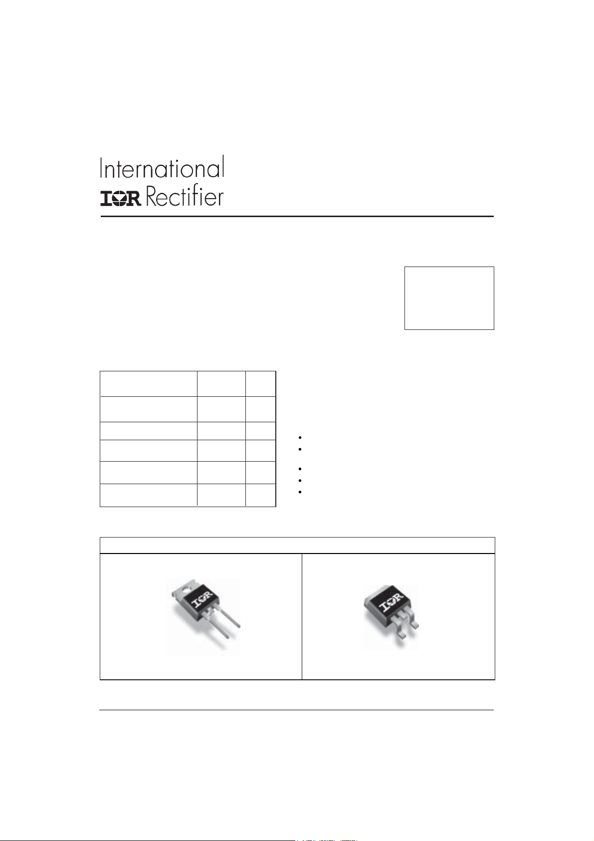
8TQ...
TO-220
Case Styles
8TQ... S
2
PAK
D
1www.irf.com
8TQ... Series
Bulletin PD-20561 rev. D 07/03
Voltage Ratings
Part number 8TQ080 8TQ100
VRMax. DC Reverse Voltage (V)
V
Max. Working Peak Reverse Voltage (V)
RWM
80 100
Absolute Maximum Ratings
Parameters 8TQ Units Conditions
I
Max. Average Forward Current 8 A 50% duty cycle @ TC = 157° C, rectangular wave form
F(AV)
* See Fig. 5
I
Max. Peak One Cycle Non-Repetitive 850 5µs Sine or 3µs Rect. pulse
FSM
Surge Current * See Fig. 7 230 10ms Sine or 6ms Rect. pulse
EASNon-Repetitive Avalanche Energy 7.50 mJ TJ = 25 °C, I
A
= 0.50 Amps, L = 60 mH
AS
IARRepetitive Avalanche Current 0.50 A Current decaying linearly to zero in 1 µsec
Frequency limited by T
J
Following any rated
load condition and
with rated V
RRM
max. VA = 1.5 x VR typical
Electrical Specifications
Parameters 8TQ Units Conditions
VFMMax. Forward Voltage Drop (1) 0.72 V @ 8A
* See Fig. 1 0.88 V @ 16A
0.58 V @ 8A
0.69 V @ 16A
IRMMax. Reverse Leakage Current (1) 0.55 mA TJ = 25 °C
* See Fig. 2 7 mA TJ = 125 °C
CTMax. Junction Capacitance 500 pF VR = 5VDC (test signal range 100Khz to 1Mhz) 25 °C
LSTypical Series Inductance 8 nH Measured lead to lead 5mm from package body
dv/dt Max. Voltage Rate of Change 10000 V/ µs
(Rated VR)
(1) Pulse Width < 300µs, Duty Cycle < 2%
TJ = 25 °C
TJ = 125 °C
VR = rated V
R
applied
Thermal-Mechanical Specifications
Parameters 8TQ Units Conditions
TJMax. Junction Temperature Range -55 to 175 °C
T
Max. Storage Temperature Range -55 to 175 °C
stg
R
Max. Thermal Resistance Junction 2.0 °C/W DC operation * See Fig. 4
thJC
to Case
R
Typical Thermal Resistance, Case to 0.50 °C/W Mounting surface , smooth and greased
thCS
Heatsink
wt Approximate Weight 2 (0.07) g (oz.)
T Mounting Torque Min. 6 (5)
Max. 12 (10)
2
Kg-cm
(Ibf-in)
www.irf.com
8TQ... Series
Bulletin PD-20238 rev. D 07/03
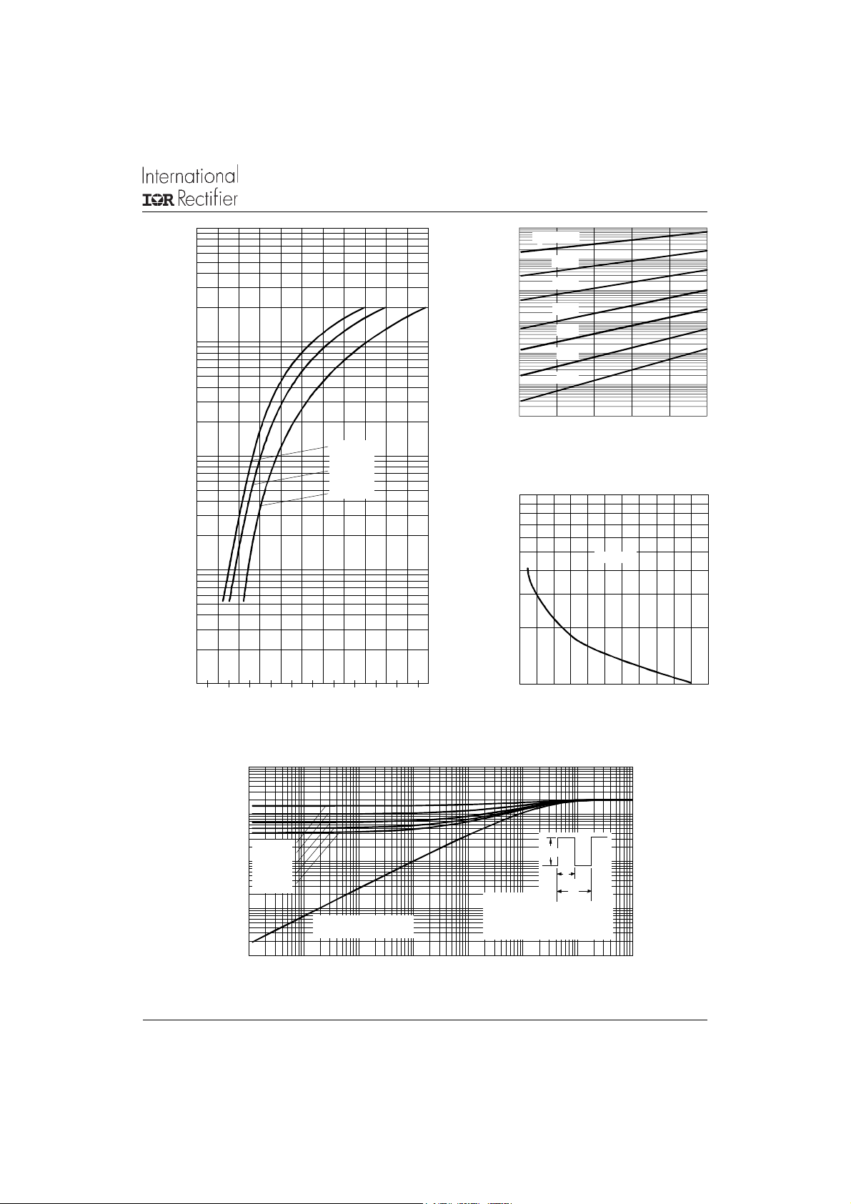
1000
100
T = 175°C
J
10
1
R
150°C
125°C
100°C
0.1
100
F
0.01
Re verse Current - I (m A)
0.001
0.0001
T = 175°C
10
Insta nta neous Forwa rd Current - I (A)
J
T = 125°C
J
T = 25°C
J
1000
T
1
75°C
50°C
25°C
0 20406080100
Reverse Volt age - V (V)
R
Fig. 2 - Typical Values of Reverse Current
Vs. Reverse Voltage
T = 25°C
J
0.1
0 0.2 0.4 0. 6 0.8 1 1.2 1.4 1.6 1.8 2 2.2
Forward Voltage Drop - V (V)
Fig. 1 - Maximum Forward Voltage Drop Characteristics
10
1
thJC
D = 0.75
D = 0.50
0.1
D = 0.33
D = 0.25
D = 0.20
0.01
Thermal Impedance Z (°C/W)
0.001
0.00001 0.0001 0.001 0.01 0.1 1 10 100
Single Pulse
( The rm a l Re si st a nc e )
t , Rectangular Pulse Duration (Seconds)
1
Fig. 4 - Maximum Thermal Impedance Z
www.irf.com
Junction Capacitance - C (pF)
100
0 102030405060708090100110
FM
Reverse Voltage - V (V)
R
Fig. 3 - Typical Junction Capacitance
Vs. Reverse Voltage
P
DM
t
1
t
Not es:
1. Duty fa ct or D = t / t
2. Pea k T = P x Z + T
J
Characteristics
thJC
2
2
1
thJC
C
DM
3

8TQ... Series
Bulletin PD-20561 rev. D 07/03
180
175
170
DC
165
160
Squ are w av e ( D = 0.50)
155
80% Rated V applied
R
150
145
Allowable Case Temperature - (°C)
see note (2)
140
024681012
Averag e Forwa rd Current - I (A)
F( A V )
Fig. 5 - Maximum Allowable Case Temperature
Vs. Average Forward Current
1000
FSM
At Any Rated Load Condition
And With Rated V Applied
Follow ing Surg e
RRM
7
D = 0.20
D = 0.25
6
D = 0.33
D = 0.50
5
D = 0.75
4
RM S Li m it
DC
3
2
Averag e Power Loss - (Watts)
1
0
024681012
Average Forward Current - I (A)
Fig. 6 - Forward Power Loss Characteristics
F( A V )
DUT
C U RREN T
MONITOR
(2) Formula used: TC = TJ - (Pd + Pd
Pd = Forward Power Loss = I
Pd
= Inverse Power Loss = VR1 x IR (1 - D); IR @ V
REV
4
Non-Repetitive Surge Current - I (A)
100
10 100 1000 10000
Sq uare Wave Pulse Duration - t (mic rosec)
Fig. 7 - Maximum Non-Repetitive Surge Current
L
IRFP460
Rg = 25 o hm
FREE- W H EEL
DIODE
40HFL40S02
Fig. 8 - Unclamped Inductive Test Circuit
) x R
thJC
x VFM @ (I
;
/ D) (see Fig. 6);
F(AV)
R1
= 80% rated V
R
REV
F(AV)
p
HI G H- SPEED
SW ITC H
Vd = 25 Volt
+
www.irf.com

Outline Table
Anode
1
3
Base
Cathode
Cathode
e
8TQ... Series
Bulletin PD-20238 rev. D 07/03
10.54 (0.41)
N/C
4.57 (0.18)
4.32 (0.17)
Base
Cathode
1
15.24 (0.60)
14.84 (0.58)
14.09 (0.55)
13.47 (0.53)
1.40 (0.05)
1.15 (0.04)
2
3
Anod
MAX.
1
1
15.49 (0.61)
14.73 (0.58)
3X
TERM 2
3
2.04 (0.080) MAX.
0.94 (0.04)
0.69 (0.03)
3
5.08 (0.20) REF.
93°
1.40 (0.055)
1.14 (0.045)
3.78 (0.15)
3.54 (0.14)
2.92 (0.11)
2.54 (0.10)
3.96 (0.16)
3.55 (0.14)
0.61 (0.02) MAX.
10.16 (0.40)
REF.
13
Conform to JEDEC outline D2Pak (SMD-220)
Dimensions in millimeters and (inches)
2
DIA.
2.61 (0.10)
2.32 (0.09)
8.89 (0.35)
REF .
0.93 (0.37)
2X
0.69 (0.27)
5.08 (0.20) REF.
6.48 (0.25)
6.23 (0.24)
6.47 (0.25)
6.18 (0.24)
4.57 (0.18)
4.32 (0.17)
0.61 (0.02) MAX.
1.32 (0.05)
1.22 (0.05)
2°
0.10 (0.004)
2.89 (0.11)
2.64 (0.10)
Conform to JEDEC outline TO-220AC
Dimensions in millimeters and (inches)
4.69 (0.18)
4.20 (0.16)
1.32 (0.05)
1.22 (0.05)
5.28 (0.21)
4.78 (0.19)
0.55 (0.02)
0.46 (0.02)
MINIMUM R ECOMMEND ED F OOTPRIN T
11.43 (0.45)
8.89 (0.35)
3.81 (0.15)
2.08 (0.08)
2X
17.78 (0.70)
2.54 (0.10)
2X
www.irf.com
5

8TQ... Series
Bulletin PD-20561 rev. D 07/03
Ordering Information Table
Device Code
8 T Q 100 S
1 5243
1 - Essential Part Number
2 - T = TO-220
3 - Q = Schottky Q Series
4 - Voltage Rating
5 -S=D2Pak
8TQ100
********************************************
* This model has been developed by *
* Wizard SPICE MODEL GENERATOR (1999) *
* (International Rectifier Corporation) *
* Contain Proprietary Information *
********************************************
* SPICE Model Diode is composed by a *
* simple diode plus paralled VCG2T *
********************************************
.SUBCKT 8TQ100 ANO CAT
D1 ANO 1 DMOD (0.07089)
*Define diode model
.MODEL DMOD D(IS=1.15938021883115E-03A,N=1.95244918720315,BV=120V,
+ IBV=5.37891460505463A,RS= 0.00127602,CJO=9.9895753025115E-09,
+ VJ=2.30070034831946,XTI=2, EG=0.758916909331649)
********************************************
*Implementation of VCG2T
VX 1 2 DC 0V
R1 2 CAT TRES 1E-6
.MODEL TRES RES(R=1,TC1=-90.2420977904848)
GP1 ANO CAT VALUE={-ABS(I(VX))*(EXP((((1.635248E-02/-90.2421)*((V(2,CAT)*1E6)/(I(VX)+1E-6)-
1))+1)*4.011038E-03*ABS(V(ANO,CAT)))-1)}
********************************************
.ENDS 8TQ100
080 = 80V
100 = 100V
Thermal Model Subcircuit
.SUBCKT 8TQ100 5 1
CTHERM1 5 4 1.45E+00
CTHERM2 4 3 4.54E+00
CTHERM3 3 2 1.09E+01
CTHERM4 2 1 1.01E+02
RTHERM1 5 4 2.49E+00
RTHERM2 4 3 5.20E-04
RTHERM1 3 2 5.43E-01
RTHERM1 2 1 3.05E-02
.ENDS 8TQ100
6
www.irf.com

8TQ... Series
Bulletin PD-20238 rev. D 07/03
This product has been designed and qualified for Industrial Level.
Data and specifications subject to change without notice.
Qualification Standards can be found on IR's Web site.
IR WORLD HEADQUARTERS: 233 Kansas St., El Segundo, California 90245, USA Tel: (310) 252-7105
TAC Fax: (310) 252-7309
Visit us at www.irf.com for sales contact information. 07/03
www.irf.com
7
 Loading...