Bulletin PD-20698 rev. B 02/04
e
Anode
1
3
2
N/C
8ETL06
8ETL06S
8ETL06-1
8ETL06FP
Ultra-low VF Hyperfast Rectifier for Discontinuous Mode PFC
Features
• Benchmark Ultra-low Forward Voltage Drop
• Hyperfast Recovery Time
• Low Leakage Current
• 175°C Operating Junction Temperature
• Fully Isolated package (V
• UL E78996 approved
= 2500 V
INS
RMS
)
Description
State of the art, ultra-low VF, soft-switching Hyperfast Rectifiers optimized for Discontinuous (Critical) Mode (DCM)
Power Factor Correction (PFC).
The minimised conduction loss, optimized stored charge and low recovery current minimize the switching losses and
reduce over dissipation in the switching element and snubbers.
The device is also intended for use as a free wheeling diode in power supplies and other power switching
applications.
Applications
AC-DC SMPS 70W-400W
e.g. Laptop & Printer AC Adaptors, Desktop PC, TV & Monitor, Games units and DVD AC-DC power supplies.
Absolute Maximum Ratings
Parameters Max Units
V
RRM
I
F(AV)
I
FSM
I
FM
TJ, T
Peak Repetitive Reverse Voltage 600 V
Average Rectified Forward Current @ TC = 160°C 8 A
@ TC = 142°C (FULLPACK)
Non Repetitive Peak Surge Current @ TJ = 25°C 175
Peak Repetitive Forward Current 16
Operating Junction and Storage Temperatures - 65 t o 175 °C
STG
VF = 0.96V typ.
I
= 8Amp
F(AV)
VR = 600V
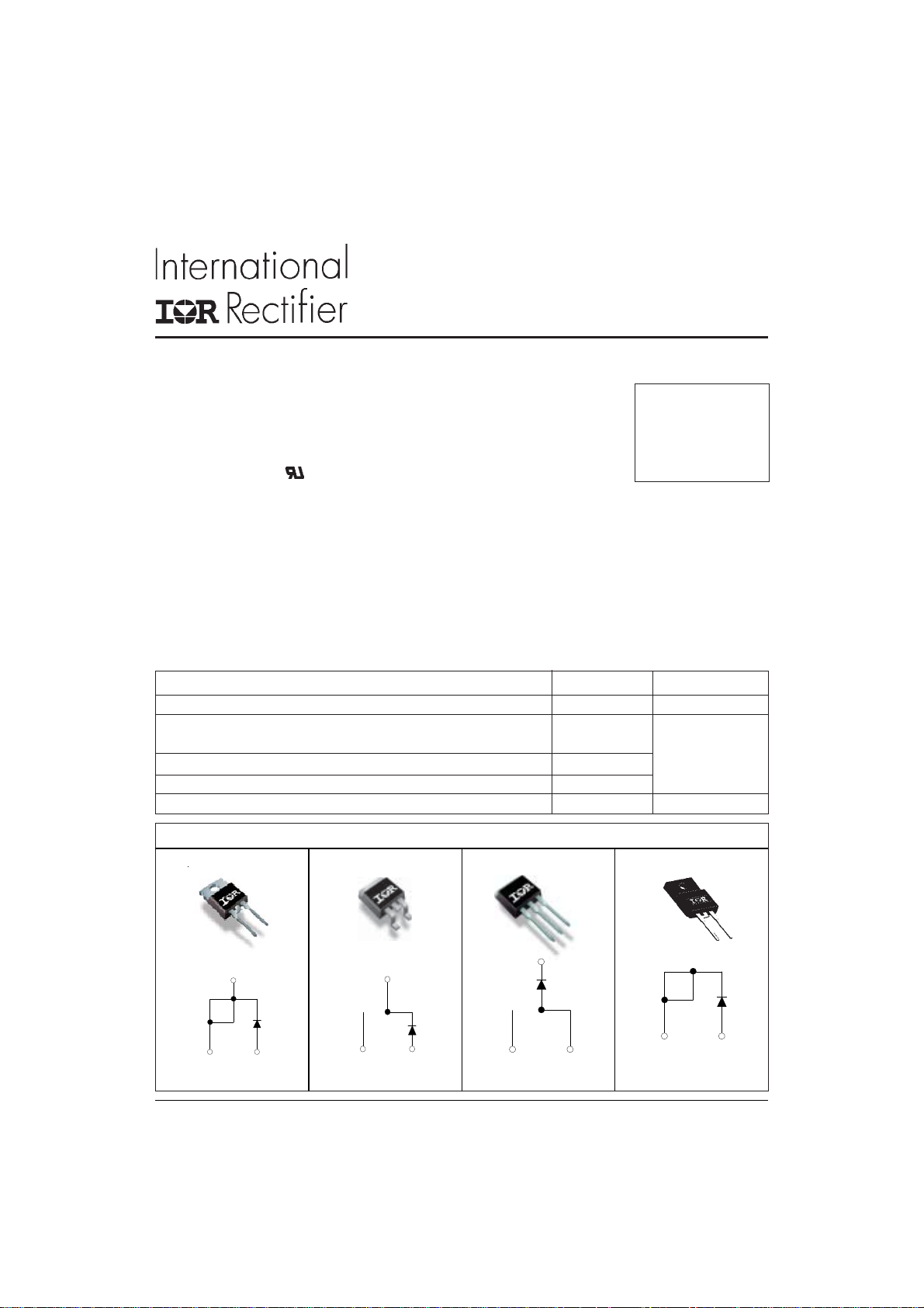
Case Styles
8ETL06
Base
Cathode
1
Cathode
TO-220AC
2
3
Anode
8ETL06S
Base
Cathode
1
N/C
D2PAK
8ETL06-1
2
3
Anod
TO-262
www.irf.com
8ETL06FP
Cathode
1
3
Anode
TO-220 FULLPACK
1

8ETL06, 8ETL06S, 8ETL06-1, 8ETL06FP
Bulletin PD-20698 rev. B 02/04
Electrical Characteristics @ T
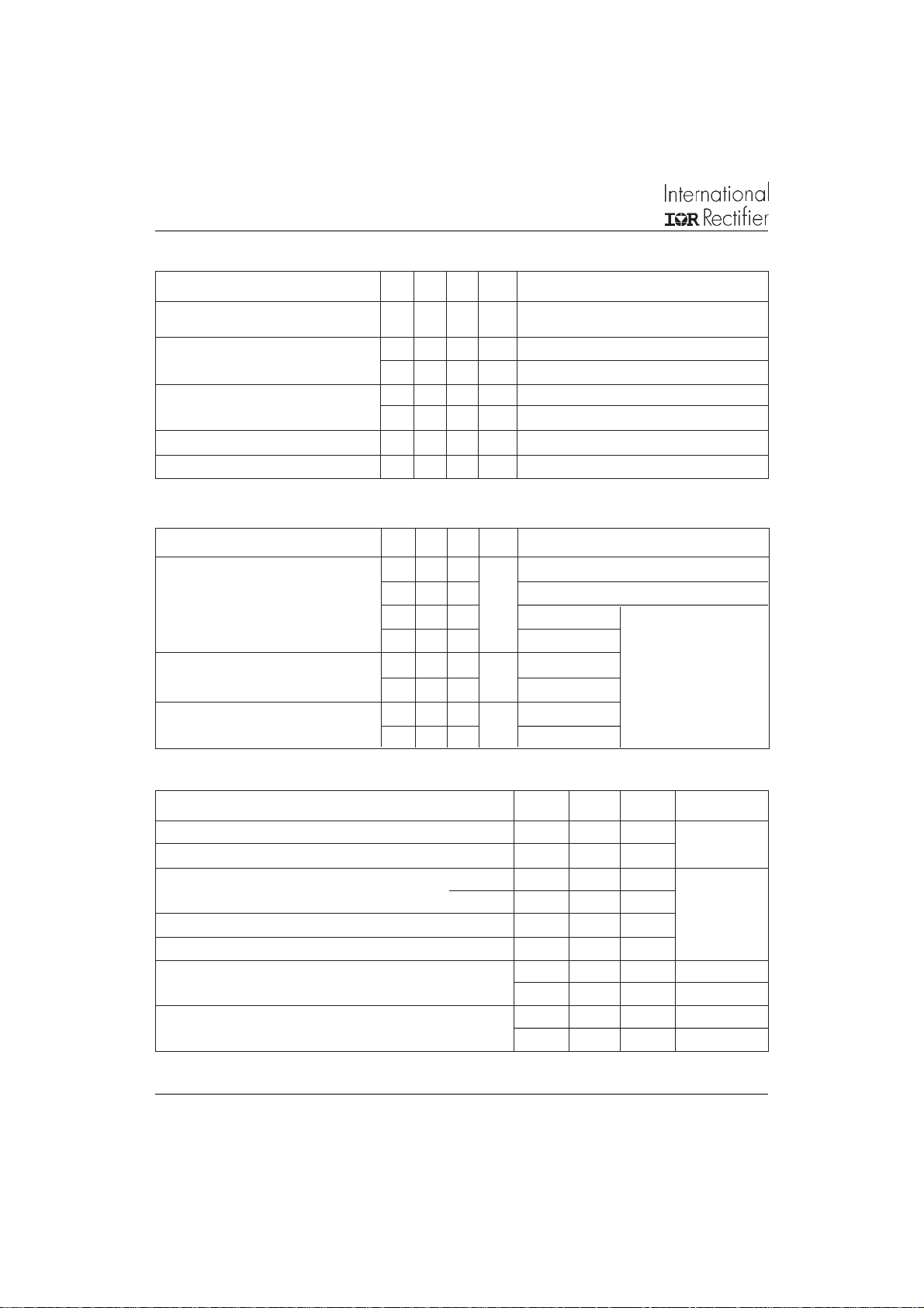
Parameters Min Typ Max Test Conditions
= 25°C (unless otherwise specified)
J
Units
VBR, VrBreakdown Voltage, 600 - - V IR = 100µA
Blocking Voltage
V
F
Forward Voltage - 0.96 1.05 V IF = 8A, TJ = 25°C
- 0.81 0.86 V IF = 8A, TJ = 150°C
I
R
Reverse Leakage Current - 0.05 5 µA VR = VR Rated
- 20 100 µA TJ = 150°C, VR = VR Rated
C
T
L
S
Junction Capacitance - 17 - pF VR = 600V
Series Inductance - 8.0 - nH Measured lead to lead 5mm from package body
Dynamic Recovery Characteristics @ TC = 25°C (unless otherwise specified)
t
rr
I
RRM
Q
Parameters Min Typ Max Test Conditions
Reverse Recovery Time - 60 100 ns IF = 1A, diF/dt = 100A/µs, VR = 30V
- 150 250 IF = 8A, diF/dt = 100A/µs, VR = 30V
- 170 - TJ = 25°C
- 250 - TJ = 125°C
Peak Recovery Current - 15 - A TJ = 25°C
-20- TJ = 125°C
rr
Reverse Recovery Charge - 1.3 - µC TJ = 25°C
- 2.6 - TJ = 125°C
Units
I
= 8A
F
diF /dt = 200A/µs
VR = 390V
Thermal - Mechanical Characteristics
Parameters Min Typ Max Units
T
J
T
Stg
R
thJC
R
thJA
R
thCS
Typical Socket Mount
Mounting Surface, Flat, Smooth and Greased
2
Max. Junction Temperature Range - - 175 °C
Max. Storage Temperature Range - 65 - 175
Thermal Resistance, Junction to Case Per Leg - 1.4 2 °C/W
Fullpack (Per Leg) - 3.4 4.3
Thermal Resistance, Junction to Ambient Per Leg - - 70
Thermal Resistance, Case to Heatsink - 0.5 -
Weight - 2.0 - g
Mounting Torque 6.0 - 12 Kg-cm
- 0.07 - (oz)
5.0 - 10 lbf.in
www.irf.com

8ETL06, 8ETL06S, 8ETL06-1, 8ETL06FP
Bulletin PD-20698 rev. B 02/04
100
10
(A)
F
1
Instantaneous Forward Current - I
T = 175˚C
J
T = 150˚C
J
T = 25˚C
J
100
Tj = 175˚C
150˚C
(µA)
R
10
1
125˚C
100˚C
75˚C
0.1
0.01
Reverse Current - I
0.001
100 200 300 400 500 600
50˚C
25˚C
Reverse Voltage - VR (V)
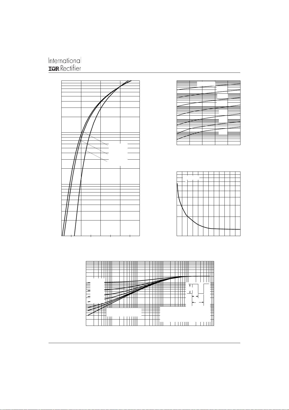
Fig. 2 - Typical Values Of Reverse Current
Vs. Reverse Voltage
100
T = 25˚C
J
( p F )
T
0.1
0.4 0.8 1.2 1.6 2
Forward Voltage Drop - VFM (V)
Fig. 1 - Typical Forward Voltage Drop Characteristics
10
(°C/W)
thJC
1
D = 0.50
D = 0.20
D = 0.10
D = 0.05
D = 0.02
D = 0.01
0.1
Single Pulse
(Thermal Resistance)
Thermal Impedance Z
0.01
0.00001 0.0001 0.001 0.01 0.1 1
t1, Rectangular Pulse Duration (Seconds)
Fig. 4 - Max. Thermal Impedance Z
www.irf.com
Junction Capacitance - C
10
0 100 200 300 400 500 600
Reverse Voltage - VR (V)
Fig. 3 - Typical Junction Capacitance
Vs. Reverse Voltage
P
DM
t
1
t
Notes:
1. Duty factor D = t1/ t2
2. Peak Tj = Pdm x ZthJC + Tc
Characteristics
thJC
2
3

8ETL06, 8ETL06S, 8ETL06-1, 8ETL06FP
Bulletin PD-20698 rev. B 02/04
10
1
D = 0.50
D = 0.20
D = 0.10
(°C/W)
thJC
D = 0.05
D = 0.02
D = 0.01
0.1
Single Pulse
(Thermal Resistance)
Thermal Impedance Z
0.01
0.00001 0.0001 0.001 0.01 0.1 1 10 100
t1, Rectangular Pulse Duration (Seconds)
Fig. 5 - Max. Thermal Impedance Z
180
175
170
165
160
Square wave (D = 0.50)
Rated Vr applied
DC
155
Allowable Case Temperature (°C)
see note (3)
150
02468101214
Average Forward Current - IF
Fig. 6 - Max. Allowable Case Temperature
Vs. Average Forward Current
(AV)
(A)
P
DM
Notes:
1. Duty factor D = t1/ t2
2. Peak Tj = Pdm x ZthJC + Tc
Characteristics (FULLPACK)
thJC
180
160
140
120
Square wave (D = 0.50)
Rated Vr applied
100
see note (3)
Allowable Case Temperature (°C)
80
02468101214
Average Forward Current - IF
Fig. 7 - Max. Allowable Case Temperature
Vs. Average Forward Current (FULLPACK)
t
1
t
2
DC
(A)
(AV)
12
10
8
6
RMS Limit
4
2
Average Power Loss ( Watts )
0
024681012
Average Forward Current - IF
Fig. 8 - Forward Power Loss Characteristics
4
DC
D = 0.01
D = 0.02
D = 0.05
D = 0.1
D = 0.2
D = 0.5
(A)
(AV)
(3) Formula used: TC = TJ - (Pd + Pd
Pd = Forward Power Loss =
I
x VFM @ (I
F(AV)
(see Fig. 8);
Pd
= Inverse Power Loss = VR1 x IR (1 - D);
REV
I
@ V
= rated V
R
R1
F(AV)
/ D)
R
) x R
thJC
;
REV
www.irf.com

8ETL06, 8ETL06S, 8ETL06-1, 8ETL06FP
Bulletin PD-20698 rev. B 02/04
450
IF = 16 A
400
IF = 8 A
350
300
250
trr ( ns )
200
150
100
V = 390V
R
50
T = 125˚C
J
T = 25˚C
J
0
100 1000
di
/dt (A/µs )
F
Fig. 9 - Typical Reverse Recovery vs. di
5000
4500
4000
3500
3000
2500
Qrr ( nC )
2000
1500
1000
500
/dt
F
Reverse Recovery Circuit
IF = 16 A
IF = 8 A
V = 390V
R
T = 125˚C
J
T = 25˚C
J
100 1000
di F /dt (A/µs )
Fig. 10 - Typical Stored Charge vs. di
/dt
F
www.irf.com
V = 200V
R
0.01
Ω
L = 70µH
D.U.T.
diF /dt
dif/dt
ADJUST
G
D
IRFP250
S
Fig. 11- Reverse Recovery Parameter Test Circuit
5

8ETL06, 8ETL06S, 8ETL06-1, 8ETL06FP
Bulletin PD-20698 rev. B 02/04
I
F
0
1
diF /dt
di /dt
t
a
f
3
t
rr
t
b
4
Q
2
I
RRM
0.75
rr
0.5
I
RRM
di(rec)M/dt
I
RRM
5
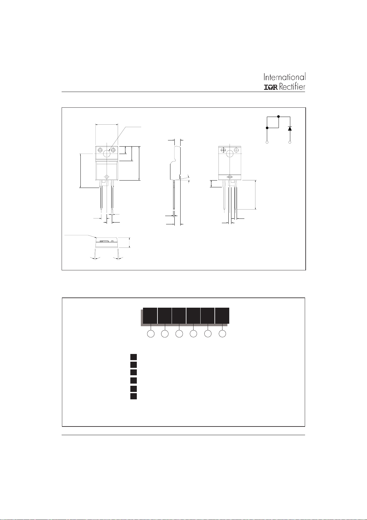
Outline Table
15.24 (0.60)
14.84 (0.58)
14.09 (0.55)
13.47 (0.53)
4.57 (0.18)
4.32 (0.17)
1. diF/dt - Rate of change of current through zero
crossing
2. I
- Peak reverse recovery current
RRM
3. t
- Reverse recovery time measured from zero
rr
crossing point of negative going IF to point where
a line passing through 0.75 I
extrapolated to zero current
RRM
and 0.50 I
Fig. 12 - Reverse Recovery Waveform and Definitions
10.54 (0.41)
MAX.
1
1.40 (0.05)
1.15 (0.04)
1
TERM 2
3
2.04 (0.080) MAX.
0.94 (0.04)
0.69 (0.03)
3
5.08 (0.20) REF.
3.78 (0.15)
3.54 (0.14)
2.92 (0.11)
2.54 (0.10)
3.96 (0.16)
3.55 (0.14)
0.61 (0.02) MAX.
DIA.
RRM
6.48 (0.25)
6.23 (0.24)
4. Qrr - Area under curve defined by t
and I
RRM
5. di
(rec) M
current during t b portion of t
1.32 (0.05)
1.22 (0.05)
2°
0.10 (0.004)
2.89 (0.11)
2.64 (0.10)
t rr x I
Q
rr
/ dt - Peak rate of change of
RRM
=
2
rr
rr
Cathode
Base
Cathode
1
2
Conforms to JEDEC Outline TO-220AC
Dimensions in millimeters and (inches)
Anode
3
6
www.irf.com

e
Outline Table
e
8ETL06, 8ETL06S, 8ETL06-1, 8ETL06FP
Bulletin PD-20698 rev. B 02/04
15.49 (0.61)
14.73 (0.58)
3X
93°
1.40 (0.055)
1.14 (0.045)
10.16 (0.40)
REF.
13
2
2.61 (0.10)
2.32 (0.09)
8.89 (0.35)
REF.
0.93 (0.37)
2X
0.69 (0 .27)
5.08 (0.20) REF.
6.47 (0.25)
6.18 (0.24)
4.57 (0.18)
4.32 (0.17)
0.61 (0.02) MAX.
4.69 (0.18)
4.20 (0.16)
1.32 (0.05)
1.22 (0.05)
5.28 (0.21)
4.78 (0.19)
0.55 (0.02)
0.46 (0.02)
MINIMUM RECOMMENDED FOOTPRINT
8.89 (0.35)
3.81 (0.15)
2.08 (0.08)
2X
11.43 (0.45)
17.78 (0.70)
2.54 (0.10)
2X
Conforms to JEDEC Outline D2PAK
Dimensions in millimeters and (inches)
N/C
Base
Cathode
1
2
3
Anod
www.irf.com
2
1
N/C
NC
3
Anod
Modified JEDEC outline TO-262
Dimensions in millimeters and (inches)
7

8ETL06, 8ETL06S, 8ETL06-1, 8ETL06FP
Bulletin PD-20698 rev. B 02/04
Outline Table
4
4
.
.
6
5
1
1
R0.7 (2 PLACES)
R0.5
2.54
TYP.
5°± 0.5°
10.6
10.4
0.9
0.7
2.54 TYP.
5°± 0.5°
HOLE ø 3.4
2
7
.
.
3
3
1
.
7
6
8
.
.
4
4
Ordering Information Table
3.1
2.8
2.6
7
.
6
8
0
.
.
5
6
1
1
0.48
0.44
2.85
2.65
10°
1
3
.
.
3
3
1.15
1.05
TYP
1.4
1.3
Cathode
7
5
.
.
3
3
1
1
1
3
Anode
Conforms to JEDEC Outline TO-220 FULLPACK
Dimensions in millimeters and (inches)
Device Code
8ET L06- 1
1 5
1 - Current Rating (8 = 8A)
2 - E = Single Diode
3 - T = TO-220, D2Pak
4 - L = Ultra-low VF HyperFast Recovery
5 - Voltage Rating (06 = 600V)
6 - "-1" = TO-262 Option
S= D2Pak
None = TO-220AC
FP = TO-220 FULLPACK
8
3
24
6
www.irf.com

8ETL06, 8ETL06S, 8ETL06-1, 8ETL06FP
Bulletin PD-20698 rev. B 02/04
This product has been designed and qualified for Industrial Level.
Data and specifications subject to change without notice.
Qualification Standards can be found on IR's Web site.
IR WORLD HEADQUARTERS: 233 Kansas St., El Segundo, California 90245, USA Tel: (310) 252-7105
TAC Fax: (310) 252-7309
Visit us at www.irf.com for sales contact information. 02/04
www.irf.com
9
 Loading...