

30CTH02PbF
K
Base
common
cathode
2
Hyperfast Rectifier,
2 x 15 A FRED Pt
30CTH02FPPbF
30CTH02PbF/30CTH02FPPbF
Vishay High Power Products
TM
FEATURES
• Hyperfast recovery time
• Low forward voltage drop
• Low leakage current
• 175 °C operating junction temperature
• Fully isolated package (V
• Lead (Pb)-free (“PbF” suffix)
• TO-220 designed and qualified for AEC Q101 level
• TO-220FP designed and qualified for industrial level
= 2500 V
INS
RMS
)
Pb-free
Available
RoHS*
COMPLIANT
Common
1
Anode
TO-220AB
2
cathode
3
Anode
Anode
TO-220 FULL-PA
1
2
Common
cathode
3
Anode
DESCRIPTION/APPLICATIONS
200 V series are the state of the art hyperfast recovery
rectifiers specifically designed with optimized performance
of forward voltage drop and hyperfast recovery time.
The planar structure and the platinum doped life time
control, guarantee the best overall performance,
ruggedness and reliability characteristics.
PRODUCT SUMMARY
trr (maximum) 30 ns
I
F(AV)
V
R
2 x 15 A
200 V
These devices are intended for use in the output rectification
stage of SMPS, UPS, dc-to-dc converters as well as
freewheeling diode in low voltage inverters and chopper
motor drives.
Their extremely optimized stored charge and low recovery
current minimize the switching losses and reduce over
dissipation in the switching element and snubbers.
ABSOLUTE MAXIMUM RATINGS
PARAMETER SYMBOL TEST CONDITIONS VALUES UNITS
Peak repetitive reverse voltage V
per diode
Average rectified forward current
Non-repetitive peak surge current I
Operating junction and storage temperatures T
(FULL-PAK) per diode T
per device 30
RRM
I
F(AV)
FSM
, T
J
TC = 159 °C
= 125 °C
C
TJ = 25 °C 200
Stg
200 V
15
A
- 65 to 175 °C
ELECTRICAL SPECIFICATIONS (TJ = 25 °C unless otherwise specified)
PARAMETER SYMBOL TEST CONDITIONS MIN. TYP. MAX. UNITS
Breakdown voltage,
blocking voltage
Forward voltage V
Reverse leakage current I
Junction capacitance C
Series inductance L
* Pb containing terminations are not RoHS compliant, exemptions may apply
Document Number: 94014 For technical questions, contact: diodes-tech@vishay.com
Revision: 11-Sep-08 1
,
V
BR
V
R
IR = 100 µA 200 - -
R
IF = 15 A - 0.92 1.05
F
I
= 15 A, TJ = 125 °C - 0.78 0.85
F
VR = VR rated - - 10
T
= 125 °C, VR = VR rated - 5 300
J
VR = 200 V - 57 - pF
T
Measured lead to lead 5 mm from package body - 8 - nH
S
V
µA
www.vishay.com
30CTH02PbF/30CTH02FPPbF
Vishay High Power Products
Hyperfast Rectifier,
2 x 15 A FRED Pt
TM
DYNAMIC RECOVERY CHARACTERISTICS (TC = 25 °C unless otherwise specified)
PARAMETER SYMBOL TEST CONDITIONS MIN. TYP. MAX. UNITS
IF = 1 A, dIF/dt = 50 A/µs, VR = 30 V - - 35
= 1 A, dIF/dt = 100 A/µs, VR = 30 V - - 30
I
Reverse recovery time t
Peak recovery current I
Reverse recovery charge Q
rr
RRM
rr
F
T
= 25 °C
J
= 125 °C - 40 -
T
J
TJ = 25 °C - 2.8 -
T
= 125 °C - 6.0 -
J
TJ = 25 °C - 37 -
T
= 125 °C - 120 -
J
I
= 15 A
F
/dt = 200 A/µs
dI
F
V
= 160 V
R
-26-
nC
THERMAL - MECHANICAL SPECIFICATIONS
PARAMETER SYMBOL TEST CONDITIONS MIN. TYP. MAX. UNITS
Maximum junction and storage
temperature range
Thermal resistance,
junction to case
Marking device
(FULL-PAK) per diode - - 3.5
per diode
T
, T
J
Stg
R
thJC
Mounting surface, flat, smooth
and greased
Case style TO-220AB 30CTH02
Case style TO-220 FULL-PAK 30CTH02FP
- 65 - 175 °C
--1.1
ns
A
°C/W
www.vishay.com For technical questions, contact: diodes-tech@vishay.com
2 Revision: 11-Sep-08
Document Number: 94014
30CTH02PbF/30CTH02FPPbF
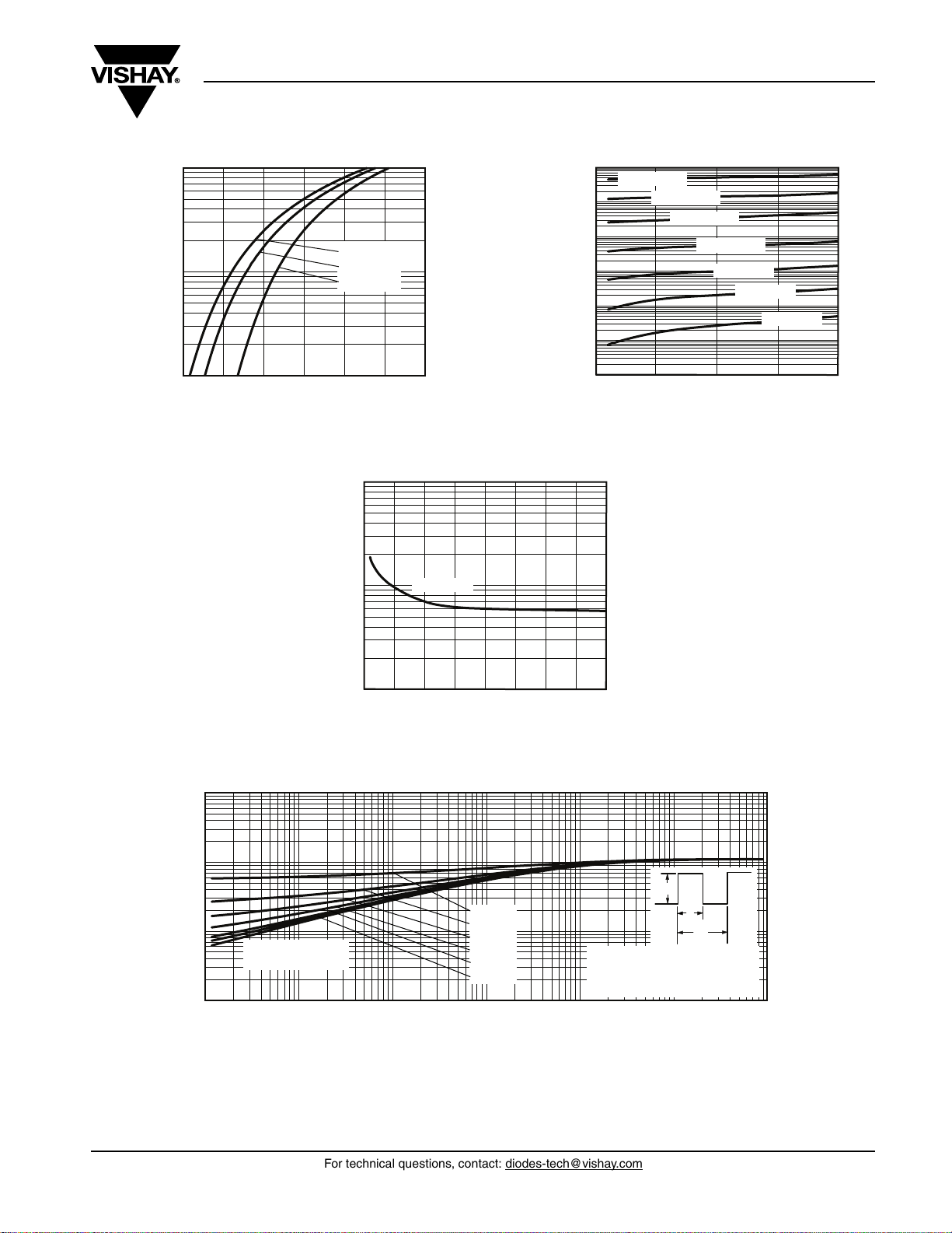
100
10
Current (A)
- Instantaneous Forward
F
I
1
0.4 0.6 0.8 1.0 1.2 1.4 1.6
VF - Forward Voltage Drop (V)
TJ = 175 °C
= 125 °C
T
J
= 25 °C
T
J
Hyperfast Rectifier,
2 x 15 A FRED Pt
TM
- Reverse Current (µA)
R
I
Vishay High Power Products
100
10
0.1
0.01
0.001
0.0001
TJ = 175 °C
TJ = 150 °C
TJ = 125 °C
1
0 100 200
50
TJ = 100 °C
TJ = 75 °C
TJ = 50 °C
TJ = 25 °C
150
VR - Reverse Voltage (V)
Fig. 1 - Typical Forward Voltage Drop Characteristics Fig. 2 - Typical Values of Reverse Current vs.
Reverse Voltage
1000
100
- Junction Capacitance (pF)
T
C
10
0 50 100 150 200
TJ = 25 °C
VR - Reverse Voltage (V)
Fig. 3 - Typical Junction Capacitance vs. Reverse Voltage
10
1
D = 0.50
0.1
Single pulse
- Thermal Impedance (°C/W)
thJC
Z
0.01
0.00001 0.0001 0.001 0.01 0.1
(thermal resistance)
D = 0.20
D = 0.10
D = 0.05
D = 0.02
D = 0.01
t1 - Rectangular Pulse Duration (s)
Fig. 4 - Maximum Thermal Impedance Z
Notes:
1. Duty factor D = t
2. Peak TJ = PDM x Z
Characteristics
thJC
P
DM
t
1
t
2
.
1/t2
+ T
thJC
C
.
110
Document Number: 94014 For technical questions, contact: diodes-tech@vishay.com
www.vishay.com
Revision: 11-Sep-08 3

30CTH02PbF/30CTH02FPPbF
Vishay High Power Products
10
1
0.1
- Thermal Impedance (°C/W)
thJC
Z
0.01
0.00001 0.0001 0.001 0.01 0.1
180
170
Square wave (D = 0.50)
160
Rated V
150
Allowable Case Temperature (°C)
140
05 25201510
Fig. 6 - Maximum Allowable Case Temperature vs.
Single pulse
(thermal resistance)
Fig. 5 - Maximum Thermal Impedance Z
applied
R
See note (1)
I
- Average Forward Current (A)
F(AV)
Average Forward Current
DC
Hyperfast Rectifier,
2 x 15 A FRED Pt
D = 0.50
D = 0.20
D = 0.10
D = 0.05
D = 0.02
D = 0.01
t1 - Rectangular Pulse Duration (s)
TM
Characteristics (FULL-PAK)
thJC
Average Power Loss (W)
P
DM
t
1
t
2
Notes:
1. Duty factor D = t
2. Peak TJ = PDM x Z
25
20
15
10
5
0
0 5 10 15 20 25
I
- Average Forward Current (A)
F(AV)
.
1/t2
+ T
thJC
C
.
110
RMS limit
D = 0.01
D = 0.02
D = 0.05
D = 0.1
D = 0.2
DC
D = 0.5
Fig. 8 - Forward Power Loss Characteristics
180
170
160
150
140
130
Square wave (D = 0.50)
120
Rated V
110
Allowable Case Temperature (°C)
See note (1)
100
05 25201510
I
applied
R
- Average Forward Current (A)
F(AV)
DC
Fig. 7 - Maximum Allowable Case Temperature vs.
Average Forward Current (FULL-PAK)
100
(ns)
rr
t
VR = 160 V
= 125 °C
T
J
= 25 °C
T
J
10
100 1000
dIF/dt (A/µs)
Fig. 9 - Typical Reverse Recovery Time vs. dI
IF = 15 A
/dt
F
Note
(1)
Formula used: TC = TJ - (Pd + Pd
Pd = Forward power loss = I
Pd
= Inverse power loss = VR1 x IR (1 - D); IR at VR1 = Rated V
REV
F(AV)
) x R
REV
x VFM at (I
;
thJC
/D) (see fig. 8);
F(AV)
R
www.vishay.com For technical questions, contact: diodes-tech@vishay.com
Document Number: 94014
4 Revision: 11-Sep-08

30CTH02PbF/30CTH02FPPbF
Hyperfast Rectifier,
2 x 15 A FRED Pt
1000
100
(nC)
rr
Q
VR = 160 V
= 125 °C
T
J
= 25 °C
T
10
100 1000
J
dIF/dt (A/µs)
Fig. 10 - Typical Stored Charge vs. dIF/dt
V
= 200 V
R
0.01 Ω
L = 70 µH
TM
Vishay High Power Products
IF = 15 A
D.U.T.
dIF/dt
adjust
G
Fig. 11 - Reverse Recovery Parameter Test Circuit
I
F
0
dIF/dt
(1)
/dt - rate of change of current
(1) dI
F
through zero crossing
(2) I
- peak reverse recovery current
RRM
- reverse recovery time measured
(3) t
rr
from zero crossing point of negative
going I
through 0.75 I
extrapolated to zero current.
to point where a line passing
F
and 0.50 I
RRM
RRM
D
IRFP250
S
(3)
t
rr
t
a
(2)
I
RRM
t
b
(4)
Q
rr
0.5 I
RRM
dI
/dt
(rec)M
0.75 I
RRM
(4) Q
- area under curve defined by t
rr
and I
RRM
trr x I
(5) dI
current during t
=
Q
rr
/dt - peak rate of change of
(rec)M
portion of t
b
(5)
rr
RRM
2
rr
Fig. 12 - Reverse Recovery Waveform and Definitions
Document Number: 94014 For technical questions, contact: diodes-tech@vishay.com
www.vishay.com
Revision: 11-Sep-08 5

30CTH02PbF/30CTH02FPPbF
Vishay High Power Products
ORDERING INFORMATION TABLE
Device code
30 C T H 02 FP PbF
1 - Current rating (30 = 30 A)
2 - C = Common cathode
3
- T = TO-220
4 - H = Hyperfast recovery
5 - Voltage rating (02 = 200 V)
6
- None = TO-220AB
7 - None = Standard production
Hyperfast Rectifier,
2 x 15 A FRED Pt
51324
FP = TO-220 FULL-PAK
PbF = Lead (Pb)-free
TM
67
Tube standard pack quantity: 50 pieces
LINKS TO RELATED DOCUMENTS
Dimensions http://www.vishay.com/doc?95040
Part marking information http://www.vishay.com/doc?95042
www.vishay.com For technical questions, contact: diodes-tech@vishay.com
6 Revision: 11-Sep-08
Document Number: 94014

TO-220AB
Assembly
lot code
Part Marking Information
Vishay High Power Products
TO-220AB, TO-220AB FULL-PAK
Example: This is a xxxxxxxx with
assembly lot code AC,
assembled on WW 19, 2001
in the assembly line “X”
xxxxxxxx
V P119X
AC
Part number
Product version (optional):
P = Lead (Pb)-free
None = Standard
Date code:
Year 1 = 2001
Week 19
Line X
TO-220AB FULL-PAK
Assem
bly
lot code
xxxxxxxFP
V P119X
A
Example: This is a xxxxxxxFP with
assembly lot code AC,
assembled on WW 19, 2001
Part number
FP = FULL-PAK
C
Product version (optional):
P = Lead (Pb)-free
None = Standard
Date code:
Year 1 = 2001
Week 19
Line X
in the assembly line “X”
Document Number: 95042 For technical questions concerning discrete products, contact: diodes-tech@vishay.com
Revision: 30-Oct-08 For technical questions concerning module products, contact: ind-modules@vishay.com
www.vishay.com
1

TO-220AB, TO-220AB FULL-PAK
DIMENSIONS FOR TO-220AB in millimeters and inches
B
(6)
E
(7)
E2
Q
D
(6)
A
Ø P
Detail B
M M
0.014 AB
(6)
H1
(7)
Seating
plane
A
A
A1
(H1)
Outline Dimensions
Vishay High Power Products
Thermal pad
(E)
13
2
D
D2
D
C
(6)
C
L1
(2)
0.015 AB
Lead tip
SYMBOL
D1
13
2
C
(6)
E1
L
Base metal Plating
e
2 x
e1
MM
MILLIMETERS INCHES
MIN. MAX. MIN. MAX. MIN. MAX. MIN. MAX.
c
Lead assignments
Diodes
1. - Anode/open
2. - Cathode
3. - Anode
NOTES SYMBOL
A
A2
View A - A
Conforms to JEDEC outline TO-220AB
MILLIMETERS INCHES
c
Section C - C and D - D
3 x b23 x b
Detail B
(b, b2)
b1, b3
A 3.56 4.83 0.140 0.190 D2 11.68 12.88 0.460 0.507 6
A1 0.51 1.40 0.020 0.055 E 9.65 10.67 0.380 0.420 3, 6
A2 2.03 2.92 0.080 0.115 E1 6.86 8.89 0.270 0.350 6
b 0.38 1.01 0.015 0.040 E2 - 0.76 - 0.030 7
b1 0.38 0.97 0.015 0.038 4 e 2.54 BSC 0.100 BSC
b2 1.14 1.78 0.045 0.070 e1 5.08 BSC 0.200 BSC
b3 1.14 1.73 0.045 0.068 4 H1 5.84 6.86 0.230 0.270 6, 7
c 0.36 0.61 0.014 0.024 L 12.70 14.73 0.500 0.580
c1 0.36 0.56 0.014 0.022 4 L1 3.55 3.96 0.140 0.150 2
D 14.22 16.51 0.560 0.650 3 Ø P 3.54 4.08 0.139 0.161
D1 8.38 9.02 0.330 0.355 Q 2.54 3.42 0.100 0.135
Notes
(1)
Dimensioning and tolerancing as per ASME Y14.5M-1994
(2)
Lead dimension and finish uncontrolled in L1
(3)
Dimension D, D1 and E do not include mold flash. Mold flash
shall not exceed 0.127 mm (0.005") per side. These dimensions
are measured at the outermost extremes of the plastic body
(4)
Dimension b1, b3 and c1 apply to base metal only
(5)
Controlling dimensions: inches
(6)
Thermal pad contour optional within dimensions E, H1, D2 and
(7)
Dimensions E2 x H1 define a zone where stamping and
singulation irregularities are allowed
(8)
Outline conforms to JEDEC TO-220, except A2 (maximum) and
D2 (minimum) where dimensions are derived from the actual
package outline
E1
Document Number: 95040 For technical questions concerning discrete products, contact: diodestech@vishay.com
www.vishay.com
Revision: 16-Nov-09 For technical questions concerning module products, contact: indmodules@vishay.com
c1
(4)
(4)
NOTES
1

Outline Dimensions
Vishay High Power Products
TO-220AB,
TO-220AB FULL-PAK
DIMENSIONS FOR TO-220AB FULL-PAK in millimeters
R 0.7
R 0.5
16.4
15.4
2.54 TYP.
(2 places)
5° ± 0.5°
10.6
10.4
3.7
3.2
1
3
2
0.9
0.7
2.54 TYP.
5° ± 0.5°
Hole Ø
7.1
6.7
4.8
4.6
3.4
3.1
16.0
15.8
Lead assignments
Diodes
1. - Anode/open
2. - Cathode
3. - Anode
0.48
0.44
2.85
2.65
2.8
2.6
10°
3.3
3.1
Conforms to JEDEC
outline TO-220 FULL-PAK
1.4
1.3
1.15
1.05
13.56
13.05
TYP.
www.vishay.com For technical questions concerning discrete products, contact: diodestech@vishay.com
2 For technical questions concerning module products, contact: indmodules@vishay.com
Document Number: 95040
Revision: 16-Nov-09

Legal Disclaimer Notice
Vishay
Disclaimer
All product specifications and data are subject to change without notice.
Vishay Intertechnology, Inc., its affiliates, agents, and employees, and all persons acting on its or their behalf
(collectively, “Vishay”), disclaim any and all liability for any errors, inaccuracies or incompleteness contained herein
or in any other disclosure relating to any product.
Vishay disclaims any and all liability arising out of the use or application of any product described herein or of any
information provided herein to the maximum extent permitted by law. The product specifications do not expand or
otherwise modify Vishay’s terms and conditions of purchase, including but not limited to the warranty expressed
therein, which apply to these products.
No license, express or implied, by estoppel or otherwise, to any intellectual property rights is granted by this
document or by any conduct of Vishay.
The products shown herein are not designed for use in medical, life-saving, or life-sustaining applications unless
otherwise expressly indicated. Customers using or selling Vishay products not expressly indicated for use in such
applications do so entirely at their own risk and agree to fully indemnify Vishay for any damages arising or resulting
from such use or sale. Please contact authorized Vishay personnel to obtain written terms and conditions regarding
products designed for such applications.
Product names and markings noted herein may be trademarks of their respective owners.
Document Number: 91000 www.vishay.com
Revision: 18-Jul-08 1
 Loading...