

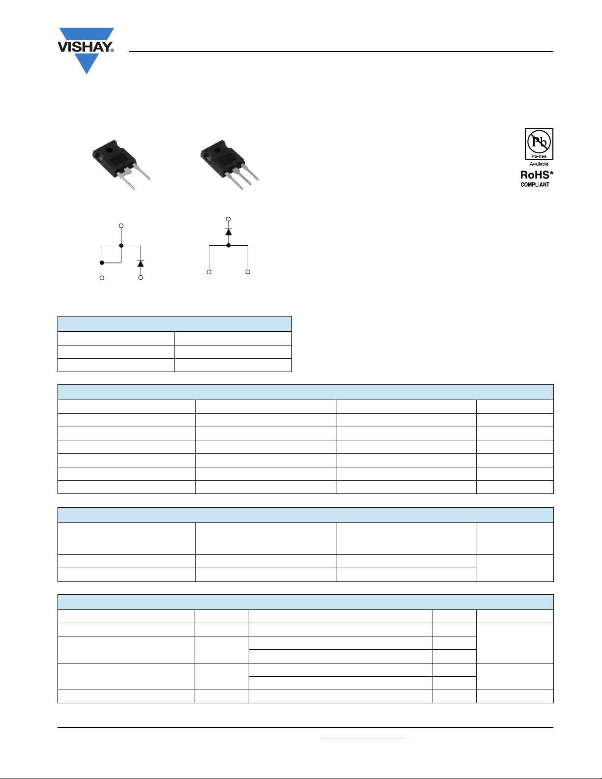
30EPF..PbF, 30CPF..PbF Soft Recovery Series
Vishay High Power Products
Fast Soft Recovery
Rectifier Diode, 30 A
30CPF..PbF30EPF..PbF
FEATURES/DESCRIPTION
The 30EPF..PbF and 30CPF..PbF soft recovery
rectifier series has been optimized for combined
short reverse recovery time and low forward
voltage drop.
Base
common
cathode
Base
common
cathode
2
2, 4
The glass passivation ensures stable reliable
operation in the most severe temperature and power cycling
conditions.
30CPF series is a drop in replacement for 25CPF series
(parallel connection only).
This product series has been designed and qualified for
industrial level.
Compliant to RoHS directive 2002/95/EC.
Anode
3
1
Cathode
TO-247AC modified
Anode
1
TO-247AC
Anode
3
APPLICATIONS
PRODUCT SUMMARY
VF at 30 A < 1.41 V
t
rr
V
RRM
95 ns
1000 V to 1200 V
• Output rectification and freewheeling in inverters,
choppers and converters
• Input rectifications where severe restrictions on conducted
EMI should be met
MAJOR RATINGS AND CHARACTERISTICS
SYMBOL CHARACTERISTICS VALUES UNITS
I
F(AV)
V
RRM
I
FSM
V
F
t
rr
T
J
Sinusoidal waveform 30 A
1000 to 1200 V
350 A
30 A, TJ = 25 °C 1.41 V
1 A, 100 A/µs 95 ns
- 40 to 150 °C
VOLTAGE RATINGS
, MAXIMUM PEAK
V
RRM
PART NUMBER
30EPF10PbF, 30CPF10PbF 1000 1100
30EPF12PbF, 30CPF12PbF 1200 1300
REVERSE VOLTAGE
V
V
, MAXIMUM NON-REPETITIVE
RSM
PEAK REVERSE VOLTAGE
V
I
RRM
AT 150 °C
mA
6
ABSOLUTE MAXIMUM RATINGS
PARAMETER SYMBOL TEST CONDITIONS VALUES UNITS
Maximum average forward current I
Maximum peak one cycle
non-repetitive surge current
Maximum I
Maximum I
* Pb containing terminations are not RoHS compliant, exemptions may apply
Document Number: 94101 For technical questions, contact: diodestech@vishay.com
Revision: 09-Dec-09 1
2
t for fusing I2t
2
√t for fusing I2√t t = 0.1 ms to 10 ms, no voltage reapplied 6360 A2√s
F(AV)
I
FSM
TC = 95 °C, 180° conduction half sine wave 30
10 ms sine pulse, rated V
10 ms sine pulse, no voltage reapplied 350
10 ms sine pulse, rated V
10 ms sine pulse, no voltage reapplied 636
applied 300
RRM
applied 450
RRM
A
2
A
s
www.vishay.com
)
30EPF..PbF, 30CPF..PbF Soft Recovery Series
Vishay High Power Products
Fast Soft Recovery
Rectifier Diode, 30 A
ELECTRICAL SPECIFICATIONS
PARAMETER SYMBOL TEST CONDITIONS VALUES UNITS
Maximum forward voltage drop V
FM
Forward slope resistance r
Threshold voltage V
Maximum reverse leakage current I
F(TO)
RM
RECOVERY CHARACTERISTICS
PARAMETER SYMBOL TEST CONDITIONS VALUES UNITS
Reverse recovery time t
Reverse recovery current I
rr
rr
Reverse recovery charge Q
Snap factor S Typical 0.6
THERMAL - MECHANICAL SPECIFICATIONS
PARAMETER SYMBOL TEST CONDITIONS VALUES UNITS
Maximum junction and storage
temperature range
Maximum thermal resistance,
junction to case
Maximum thermal resistance,
junction to ambient
Typical thermal resistance,
case to heatsink
Approximate weight
Mounting torque
maximum 12 (10)
Marking device
minimum 6 (5)
T
, T
J
R
thJC
R
thJA
R
thCS
30 A, TJ = 25 °C 1.41 V
t
rr
Stg
TJ = 150 °C
TJ = 25 °C
T
= 150 °C 6
J
IF at 30 Apk
25 A/µs
25 °C
V
= Rated V
R
450 ns
6.1 A
2.16 µC
RRM
10.09 mΩ
0.992 V
0.1
- 40 to 150 °C
DC operation 0.8
40
Mounting surface, smooth and greased 0.2
6g
0.21 oz.
Case style TO-247AC modified (JEDEC)
Case style TO-247AC
I
FM
dir
dt
30EPF10
30EPF12
30CPF10
30CPF12
t
t
atb
rr
kgf · cm
(lbf · in)
mA
I
RM(REC
°C/W
t
Q
rr
www.vishay.com For technical questions, contact: diodestech@vishay.com
Document Number: 94101
2 Revision: 09-Dec-09
30EPF..PbF, 30CPF..PbF Soft Recovery Series
150
140
130
120
110
100
Temperature (°C)
Maximum Allowable Case
90
80
150
140
130
120
110
100
Temperature (°C)
Maximum Allowable Case
90
80
Fast Soft Recovery
Rectifier Diode, 30 A
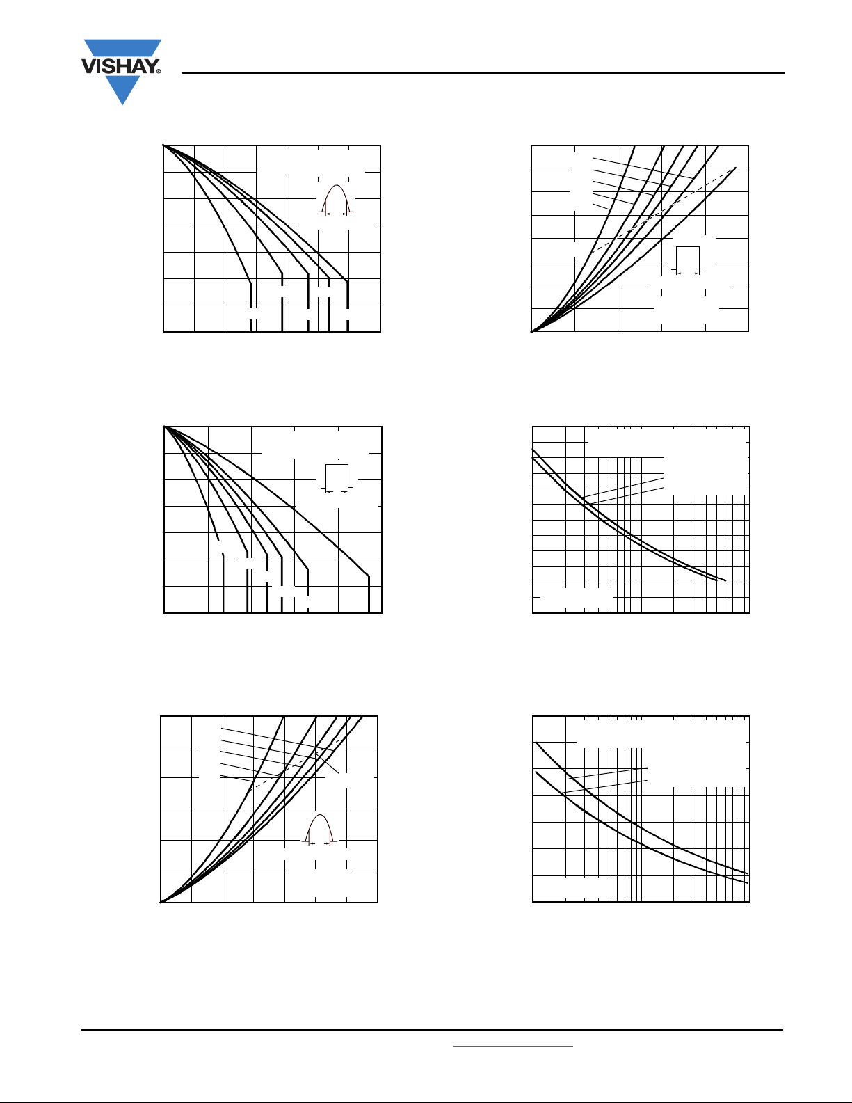
30.PF.. Series
(DC) = 0.8 K/W
R
thJC
Ø
Conduction angle
60°
30°
5
0
15
10 35
Average Forward Current (A)
Fig. 1 - Current Rating Characteristics
30.PF.. Series
R
thJC
30°
60°
90°
120°
10 20
030
Average Forward Current (A)
Fig. 2 - Current Rating Characteristics
120°
90°
20
25
(DC) = 0.8 K/W
Ø
Conduction period
180°
40
180°
30
DC
50
80
70
60
50
40
30
Power Loss (W)
20
Maximum Average Forward
10
350
300
250
200
150
Forward Current (A)
Peak Half Sine Wave
100
50
Vishay High Power Products
180°
120°
90°
60°
30°
RMS limit
Conduction period
30.PF.. Series
T
= 150 °C
0
10 30
0
20
J
Average Forward Current (A)
Fig. 4 - Forward Power Loss Characteristics
At any rated load condition and with
rated V
30.PF.. Series
1 10 100
applied following surge.
RRM
Initial TJ = 150 °C
at 60 Hz 0.0083 s
at 50 Hz 0.0100 s
Number of Equal Amplitude Half Cycle
Current Pulses (N)
Fig. 5 - Maximum Non-Repetitive Surge Current
DC
Ø
40
50
60
50
40
30
20
Power Loss (W)
Maximum Average Forward
10
180°
120°
90°
60°
30°
Conduction angle
0
0
10 155
20
RMS limit
Ø
30.PF.. Series
T
= 150 °C
J
25
Average Forward Current (A)
Fig. 3 - Forward Power Loss Characteristics
35
30
400
350
300
250
200
150
Forward Current (A)
Peak Half Sine Wave
100
50
Maximum non-repetitive surge current
versus pulse train duration.
Initial TJ = 150 °C
No voltage reapplied
Rated V
30.PF.. Series
0.01 0.1
RRM
reapplied
1
Pulse Train Duration (s)
Fig. 6 - Maximum Non-Repetitive Surge Current
Document Number: 94101 For technical questions, contact: diodestech@vishay.com
www.vishay.com
Revision: 09-Dec-09 3
30EPF..PbF, 30CPF..PbF Soft Recovery Series
Vishay High Power Products
1000
100
10
Instantaneous Forward Current (A)
1
- Maximum Reverse
rr
t
Recovery Time (µs)
0.7
0.6
0.5
0.4
0.3
0.2
0.1
30.PF.. Series
= 25 °C
T
J
Fast Soft Recovery
Rectifier Diode, 30 A
TJ = 25 °C
= 150 °C
T
J
30.PF.. Series
- Maximum Reverse
rr
Q
Recovery Charge (µC)
5
6
5
4
3
2
1
024
Instantaneous Forward Voltage (V)
Fig. 7 - Forward Voltage Drop Characteristics
I
= 30 A
FM
= 20 A
I
FM
IFM = 10 A
I
= 5 A
FM
= 1 A
I
FM
613
30.PF.. Series
= 25 °C
T
J
IFM = 30 A
IFM = 20 A
IFM = 10 A
IFM = 5 A
IFM = 1 A
0
0 50 100 200
dI/dt - Rate of Fall of Forward Current (A/µs)
Fig. 8 - Recovery Time Characteristics, T
1.2
1.0
0.8
0.6
0.4
- Maximum Reverse
Recovery Time (µs)
rr
t
0.2
0
0 50 100 150 200
dI/dt - Rate of Fall of Forward Current (A/µs)
Fig. 9 - Recovery Time Characteristics, T
150
= 25 °C
J
30.PF.. Series
= 150 °C
T
J
IFM = 30 A
= 20 A
I
FM
I
= 10 A
FM
I
= 5 A
FM
= 1 A
I
FM
= 150 °C
J
0
0 50 100 200
dI/dt - Rate of Fall of Forward Current (A/µs)
Fig. 10 - Recovery Charge Characteristics, T
10
30.PF.. Series
= 150 °C
T
J
8
6
4
- Maximum Reverse
rr
Recovery Charge (µC)
Q
2
0
0 50 100 150 200
dI/dt - Rate of Fall of Forward Current (A/µs)
Fig. 11 - Recovery Charge Characteristics, T
150
IFM = 30 A
IFM = 1 A
J
IFM = 20 A
IFM = 10 A
IFM = 5 A
= 150 °C
J
= 25 °C
www.vishay.com For technical questions, contact: diodestech@vishay.com
Document Number: 94101
4 Revision: 09-Dec-09

30EPF..PbF, 30CPF..PbF Soft Recovery Series
Fast Soft Recovery
Vishay High Power Products
Rectifier Diode, 30 A
- Maximum Reverse
Recovery Current (A)
rr
I
25
30.PF.. Series
= 25 °C
T
J
20
15
10
5
0
0 50 100 150 200
IFM = 30 A
IFM = 20 A
IFM = 10 A
IFM = 5 A
IFM = 1 A
dI/dt - Rate of Fall of Forward Current (A/µs)
Fig. 12 - Recovery Current Characteristics, TJ = 25 °C Fig. 13 - Recovery Current Characteristics, TJ = 150 °C
1
- Maximum Reverse
Recovery Current (A)
rr
I
35
30.PF.. Series
T
= 150 °C
30
J
25
20
15
10
5
0
0 50 100 150 200
IFM = 30 A
dI/dt - Rate of Fall of Forward Current (A/µs)
Steady state value
(DC operation)
IFM = 20 A
IFM = 10 A
IFM = 5 A
IFM = 1 A
0.1
Single pulse
0.01
- Transient Thermal Impedance (K/W)
thJC
Z
Fig. 14 - Thermal Impedance Z
D = 0.50
D = 0.33
D = 0.25
D = 0.17
D = 0.08
Square Wave Pulse Duration (s)
Characteristics
thJC
30.PF.. Series
1
100.0001 0.001 0.01 0.1
Document Number: 94101 For technical questions, contact: diodestech@vishay.com
www.vishay.com
Revision: 09-Dec-09 5

30EPF..PbF, 30CPF..PbF Soft Recovery Series
Vishay High Power Products
ORDERING INFORMATION TABLE
Device code
30 E P F 12 PbF
1 - Current rating (30 = 30 A)
2 - Circuit configuration:
3 - Package:
4 - Type of silicon:
5 - Voltage code x 100 = V
6 - None = Standard production
Fast Soft Recovery
Rectifier Diode, 30 A
51324
E = Single diode
C = Single diode, 3 pins
P = TO-247AC modified
F = Fast recovery
RRM
PbF = Lead (Pb)-free
6
10 = 1000 V
12 = 1200 V
LINKS TO RELATED DOCUMENTS
Dimensions
Part marking information
SPICE model www.vishay.com/doc?95184
TO-247AC modified www.vishay.com/doc?95253
TO-247AC www.vishay.com/doc?95223
TO-247AC modified www.vishay.com/doc?95255
TO-247AC www.vishay.com/doc?95226
www.vishay.com For technical questions, contact: diodestech@vishay.com
6 Revision: 09-Dec-09
Document Number: 94101

DIMENSIONS in millimeters and inches
Outline Dimensions
Vishay High Power Products
TO-247
(2) R/2
2 x R
(5) L1
0.10 AC
Planting
B
D
(2)
C
2 x b2
3 x b
MM
(c)
Section C - C, D - D, E - E
E
1
2
b4
(b1, b3, b5)
(b, b2, b4)
(3)
E/2
3
(4)
2 x e
S
D
L
Base metal
c1
See view B
A
A2
A
D
A
C
A1
DDE E
View B
A
(6)
Ø P
MM
Ø K BD
D2
Thermal pad
Lead assignments
HEXFET
1. - Gate
2. - Drain
3. - Source
4. - Drain
C
C
IGBTs, CoPAK
1. - Gate
2. - Collector
3. - Emitter
4. - Collector
4
(4)
E1
MM
0.01 BD
View A - A
(Datum B)
FP1
D1 (4)
Diodes
1. - Anode/open
2. - Cathode
3. - Anode
SYMBOL
MILLIMETERS INCHES
MIN. MAX. MIN. MAX. MIN. MAX. MIN. MAX.
NOTES SYMBOL
MILLIMETERS INCHES
NOTES
A 4.65 5.31 0.183 0.209 D2 0.51 1.30 0.020 0.051
A1 2.21 2.59 0.087 0.102 E 15.29 15.87 0.602 0.625 3
A2 1.50 2.49 0.059 0.098 E1 13.72 - 0.540 -
b 0.99 1.40 0.039 0.055 e 5.46 BSC 0.215 BSC
b1 0.99 1.35 0.039 0.053 FK 2.54 0.010
b2 1.65 2.39 0.065 0.094 L 14.20 16.10 0.559 0.634
b3 1.65 2.37 0.065 0.094 L1 3.71 4.29 0.146 0.169
b4 2.59 3.43 0.102 0.135 N 7.62 BSC 3
b5 2.59 3.38 0.102 0.133 FP 3.56 3.66 0.14 0.144
c 0.38 0.86 0.015 0.034 FP1 - 6.98 - 0.275
c1 0.38 0.76 0.015 0.030 Q 5.31 5.69 0.209 0.224
D 19.71 20.70 0.776 0.815 3 R 0.452 5.49 0.178 0.216
D1 13.08 - 0.515 - 4 S 5.51 BSC 0.217 BSC
Notes
(1)
Dimensioning and tolerancing per ASME Y14.5M-1994
(2)
Contour of slot optional
(3)
Dimension D and E do not include mold flash. Mold flash shall not exceed 0.127 mm (0.005") per side. These dimensions are measured at
the outermost extremes of the plastic body
(4)
Thermal pad contour optional with dimensions D1 and E1
(5)
Lead finish uncontrolled in L1
(6)
Ø P to have a maximum draft angle of 1.5 to the top of the part with a maximum hole diameter of 3.91 mm (0.154")
(7)
Outline conforms to JEDEC outline TO-247 with exception of dimension c
Document Number: 95223 For technical questions concerning discrete products, contact: diodes-tech@vishay.com
www.vishay.com
Revision: 11-Mar-08 For technical questions concerning module products, contact: ind-modules@vishay.com
1

Assembly
lot code
xxxxxxx
V P119X
A
Part Marking Information
Vishay High Power Products
TO-247
Example: This is a xxxxxxx with
Part number
C
Product version (optional):
P = Lead (Pb)-free
None = Standard
Date code:
Year 1 = 2001
Week 19
Line X
assembly lot code AC,
assembled on WW 19, 2001
in the assembly line ”X”
Document Number: 95226 For technical questions concerning discrete products, contact: diodes-tech@vishay.com
Revision: 28-Nov-08 For technical questions concerning module products, contact: ind-modules@vishay.com
www.vishay.com
1

DIMENSIONS in millimeters and inches
(3)
B
(2) R/2
D
E
E/2
S
TO-247 modified
A
A2
A
Outline Dimensions
Vishay High Power Products
A
D2
(6)
ΦP
(Datum B)
ΦP1
SYMBOL
2 x R
(2)
1
2
(5) L1
C
2 x b2
3 x b
Planting
(c)
Section C - C, D - D, E - E
b4
(b1, b3, b5)
(b, b2, b4)
MILLIMETERS INCHES
MIN. MAX. MIN. MAX. MIN. MAX. MIN. MAX.
3
(4)
2 x e
D
L
See view B
Base metal
c1
D
A
C
A1
DDE E
C
C
View B
NOTES SYMBOL
Thermal pad
Lead assignments
HEXFET
1. - Gate
2. - Drain
3. - Source
4. - Drain
IGBTs, CoPAK
1. - Gate
2. - Collector
3. - Emitter
4. - Collector
4
(4)
E1
View A - A
MILLIMETERS INCHES
D1 (4)
Diodes
1. - Anode/open
2. - Cathode
3. - Anode
NOTES
A 4.65 5.31 0.183 0.209 D2 0.51 1.30 0.020 0.051
A1 2.21 2.49 0.059 0.098 E 15.29 15.87 0.602 0.625 3
A2 1.50 0.098 1.50 2.49 E1 13.72 - 0.540 -
b 0.99 1.40 0.039 0.055 e 5.46 BSC 0.215 BSC
b1 0.99 1.35 0.039 0.053 ΦK 2.54 0.010
b2 1.65 2.39 0.065 0.094 L 14.20 16.10 0.559 0.634
b3 1.65 2.37 0.065 0.094 L1 3.71 4.29 0.146 0.169
b4 2.59 3.43 0.102 0.135 N 7.62 BSC 3
b5 2.59 3.38 0.102 0.133 ΦP 3.56 3.66 0.14 0.144
c 0.38 0.86 0.015 0.034 ΦP1 - 6.98 - 0.275
c1 0.38 0.76 0.015 0.030 Q 5.31 5.69 0.209 0.224
D 19.71 20.70 0.776 0.815 3 R 0.452 5.49 0.178 0.216
D1 13.08 - 0.515 - 4 S 5.51 BSC 0.217 BSC
Notes
(1)
Dimensioning and tolerance per ASME Y14.5M-1994
(2)
Contour of slot optional
(3)
Dimension D and E do not include mold flash. Mold flash shall not exceed 0.127 mm (0.005") per side. These dimensions are measured at
the outermost extremes of the plastic body
(4)
Thermal pad contour optional with dimensions D1 and E1
(5)
Lead finish uncontrolled in L1
(6)
ΦP to have a maximum draft angle of 1.5 to the top of the part with a maximum hole diameter of 3.91 mm (0.154")
(7)
Outline conforms to JEDEC outline TO-247 with exception of dimension c
Document Number: 95253 For technical questions concerning discrete products, contact: diodes-tech@vishay.com
www.vishay.com
Revision: 11-Mar-08 For technical questions concerning module products, contact: ind-modules@vishay.com
1

Assembly
lot code
xxxxxxx
V P119X
A
Part Marking Information
Vishay High Power Products
TO-247 modified
Example: This is a xxxxxxx with
assembly lot code AC,
Part number
C
Product version (optional):
P = Lead (Pb)-free
None = Standard
Date code:
Year 1 = 2001
Week 19
Line X
assembled on WW 19, 2001
in the assembly line ”X”
Document Number: 95255 For technical questions concerning discrete products, contact: diodes-tech@vishay.com
Revision: 28-Nov-08 For technical questions concerning module products, contact: ind-modules@vishay.com
www.vishay.com
1

Legal Disclaimer Notice
Vishay
Disclaimer
All product specifications and data are subject to change without notice.
Vishay Intertechnology, Inc., its affiliates, agents, and employees, and all persons acting on its or their behalf
(collectively, “Vishay”), disclaim any and all liability for any errors, inaccuracies or incompleteness contained herein
or in any other disclosure relating to any product.
Vishay disclaims any and all liability arising out of the use or application of any product described herein or of any
information provided herein to the maximum extent permitted by law. The product specifications do not expand or
otherwise modify Vishay’s terms and conditions of purchase, including but not limited to the warranty expressed
therein, which apply to these products.
No license, express or implied, by estoppel or otherwise, to any intellectual property rights is granted by this
document or by any conduct of Vishay.
The products shown herein are not designed for use in medical, life-saving, or life-sustaining applications unless
otherwise expressly indicated. Customers using or selling Vishay products not expressly indicated for use in such
applications do so entirely at their own risk and agree to fully indemnify Vishay for any damages arising or resulting
from such use or sale. Please contact authorized Vishay personnel to obtain written terms and conditions regarding
products designed for such applications.
Product names and markings noted herein may be trademarks of their respective owners.
Document Number: 91000 www.vishay.com
Revision: 18-Jul-08 1
 Loading...