

PRODUCT SUMMARY
2N4416/2N4416A/SST4416
Vishay Siliconix
N-Channel JFETs
Part Number V
2N4416 −v6 −30 4.5 5
2N4416A −2.5 to −6 −35 4.5 5
SST4416 −v6 −30 4.5 5
GS(off)
(V) V
(BR)GSS
Min (V) gfs Min (mS) I
Min (mA)
DSS
FEATURES BENEFITS APPLICATIONS
D Excellent High-Frequency Gain:
2N4416/A, Gps 13 dB (typ) @
400 MHz
D Very Low Noise: 3 dB (typ) @
400 MHz
D Very Low Distortion
D High AC/DC Switch Off-Isolation
D Wideband High Gain
D Very High System Sensitivity
D High Quality of Amplification
D High-Speed Switching Capability
D High Low-Level Signal Amplification
D High-Frequency Amplifier/Mixer
D Oscillator
D Sample-and-Hold
D Very Low Capacitance Switches
DESCRIPTION
The 2N4416/2N4416A/SST4416 n-channel JFETs are
designed to provide high-performance amplification at high
frequencies.
The TO-206AF (TO-72) hermetically-sealed package is
available with full military processing (see Military
Information.) The TO-236 (SOT-23) package provides a
low-cost option and is available with tape-and-reel options
(see Packaging Information). For similar products in the
TO-226AA (TO-92) package, see the J304/305 data sheet.
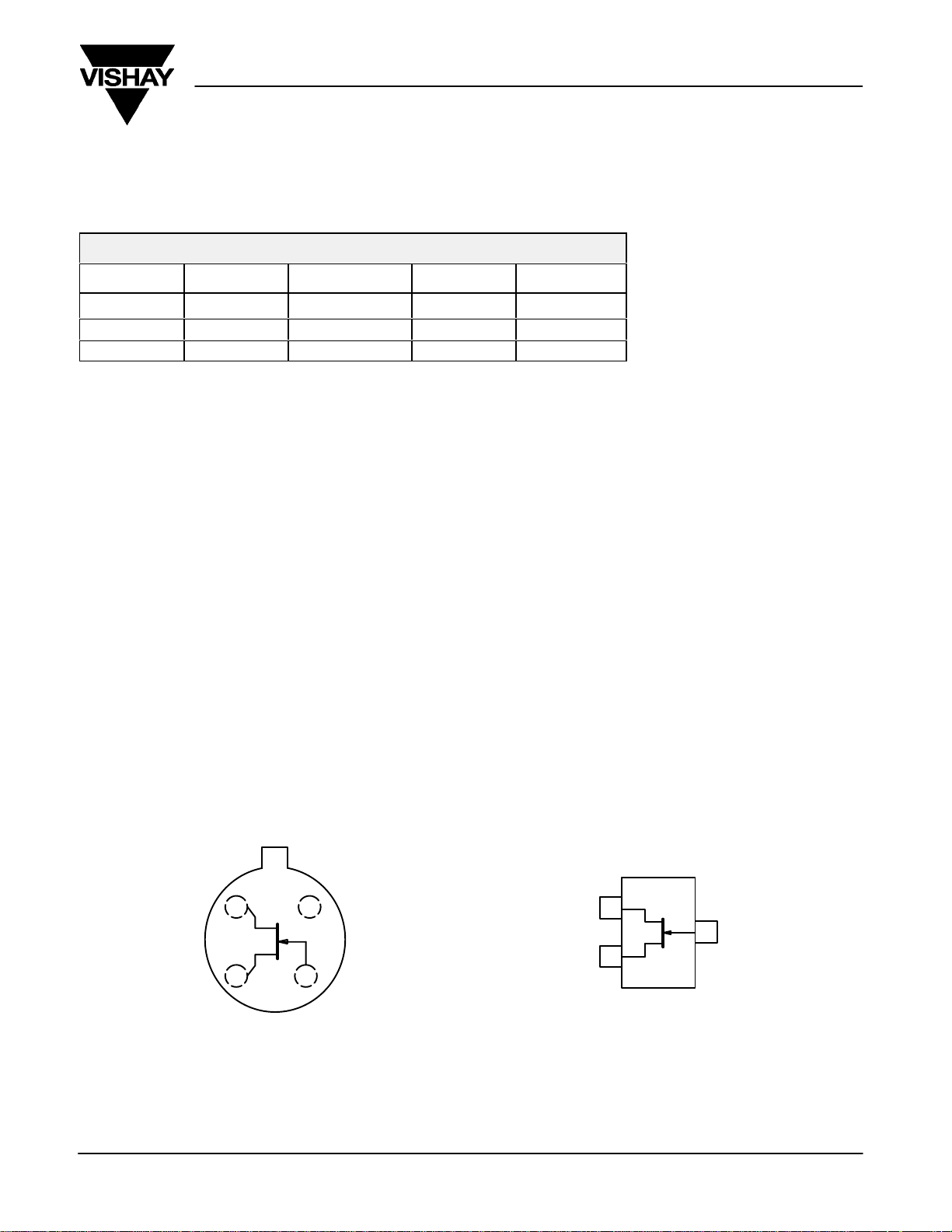
TO-206AF
(TO-72)
S C
1
23
D G
Top View
2N4416
2N4416A
For applications information see AN104.
Document Number: 70242
S-50147—Rev. H, 24-Jan-05
TO-236
(SOT-23)
4
1
D
S
2
Top View
SST4416 (H1)*
*Marking Code for TO-236
G
3
www.vishay.com
1
2N4416/2N4416A/SST4416
V
VDS = 15 V, VGS = 0 V
Vishay Siliconix
ABSOLUTE MAXIMUM RATINGS
Gate-Drain, Gate-Source Voltage :
Gate Current 10 mA. . . . . . . . . . . . . . . . . . . . . . . . . . . . . . . . . . . . . . . . . . . . . . . . .
Lead Temperature 300 _C. . . . . . . . . . . . . . . . . . . . . . . . . . . . . . . . . . . . . . . . . . .
Storage Temperature : (2N Prefix) −65 to 200 _C. . . . . . . . . . . . . . . . . .
Stresses beyond those listed under “Absolute Maximum Ratings” may cause permanent damage to the device. These are stress ratings only , and functional operation
of the device at these or any other conditions beyond those indicated in the operational sections of the specifications is not implied. Exposure to absolute maximum
rating conditions for extended periods may affect device reliability .
(2N/SST4416) −30 V. . . . . . . . . . . . . . . . . . . . .
(2N4416A) −35 V. . . . . . . . . . . . . . . . . . . . . . . . .
(SST Prefix) −65 to 150_C. . . . . . . . . . . . . . . . .
SPECIFICATIONS (TA = 25_C UNLESS NOTED)
Parameter Symbol Test Conditions TypaMin Max Min Max Min Max Unit
Static
Gate-Source
Breakdown Voltage
Gate-Source Cutoff Voltage V
Saturation Drain Current
Gate Reverse Current I
Gate Operating Current I
Drain Cutoff Current
Drain-Source On-Resistance
Gate-Source
Forward Voltage
b
c
c
c
Dynamic
Common-Source
Forward Transconductance
Common-Source
Output Conductance
Common-Source
Input Capacitance
Common-Source
Reverse Transfer Capacitance
Common-Source
Output Capacitance
Equivalent Input
Noise Voltage
c
b
b
V
(BR)GSS
GS(off)
I
DSS
GSS
I
D(off)
r
DS(on)
V
GS(F)
g
g
C
C
C
e
G
fs
os
iss
rss
oss
IG = −1 mA , VDS = 0 V
VDS = 15 V, ID = 1 nA −3 −6 −2.5 −6 −6
VDS = 15 V, VGS = 0 V 10 5 15 5 15 5 15 mA
VGS = −20 V, VDS = 0 V (2N) −2 −100 −100 pA
VGS = −15 V, VDS = 0 V (SST) −0.002 −1
VDG = 10 V, ID = 1 mA −20
VDS = 10 V, VGS = −6 V 2
VGS = 0 V, ID = 300 mA
IG = 1 mA , VDS = 0 V 0.7 V
VDS = 15 V, VGS = 0 V
f = 1 kHz
VDS = 15 V, VGS = 0 V
f = 1 MHz
n
VDS = 10 V, VGS = 0 V
f = 1 kHz
Operating Junction Temperature −55 to 150 _C. . . . . . . . . . . . . . . . . . . . . . . . .
Power Dissipation : (2N Prefix)
Notes
a. Derate 2.4 mW/_C above 25_C
b. Derate 2.8 mW/_C above 25_C
(SST Prefix)
a
b
Limits
2N4416 2N4416A SST4416
−36 −30 −35 −30
TA = 150_C
TA = 125_C
−4 −100 −100
−0.6
150
6 4.5 7.5 4.5 7.5 4.5 7.5 mS
15 50 50 50
2.2 4 4
0.7 0.8 0.8
1 2 2
6
300 mW. . . . . . . . . . . . . . . . . . . . . .
350 mW. . . . . . . . . . . . . . . . . . . .
V
nA
pA
W
mS
pF
nV⁄
√Hz
www.vishay.com
2
Document Number: 70242
S-50147—Rev. H, 24-Jan-05
2N4416/2N4416A/SST4416
DS GS
m
Vishay Siliconix
HIGH-FREQUENCY SPECIFICATIONS FOR 2N4416/2N4416A (TA = 25_C UNLESS NOTED)
Limits
100 MHz 400 MHz
Parameter Symbol Test Conditions
Min Max Min Max Unit
Common Source Input Conductance
Common Source Input Susceptance
Common Source Output Conductance
Common Source Output Susceptance
Common Source Forward Transconductance
Common-Source Power Gain
Noise Figure
Notes
a. Typical values are for DESIGN AID ONLY, not guaranteed nor subject to production testing. NH
b. Pulse test: PW v300 ms duty cycle v3%.
c. This parameter not registered with JEDEC.
d. Not a production test.
d
d
d
d
d
d
d
g
iss
b
iss
g
oss
b
oss
g
fs
G
ps
NF
VDS = 15 V, VGS = 0 V 75 100
VDS = 15 V, ID = 5 mA 18 10
RG = 1 kW
100 1,000
2,500 10,000
1,000 4,000
4,000
2 4
mS
dB
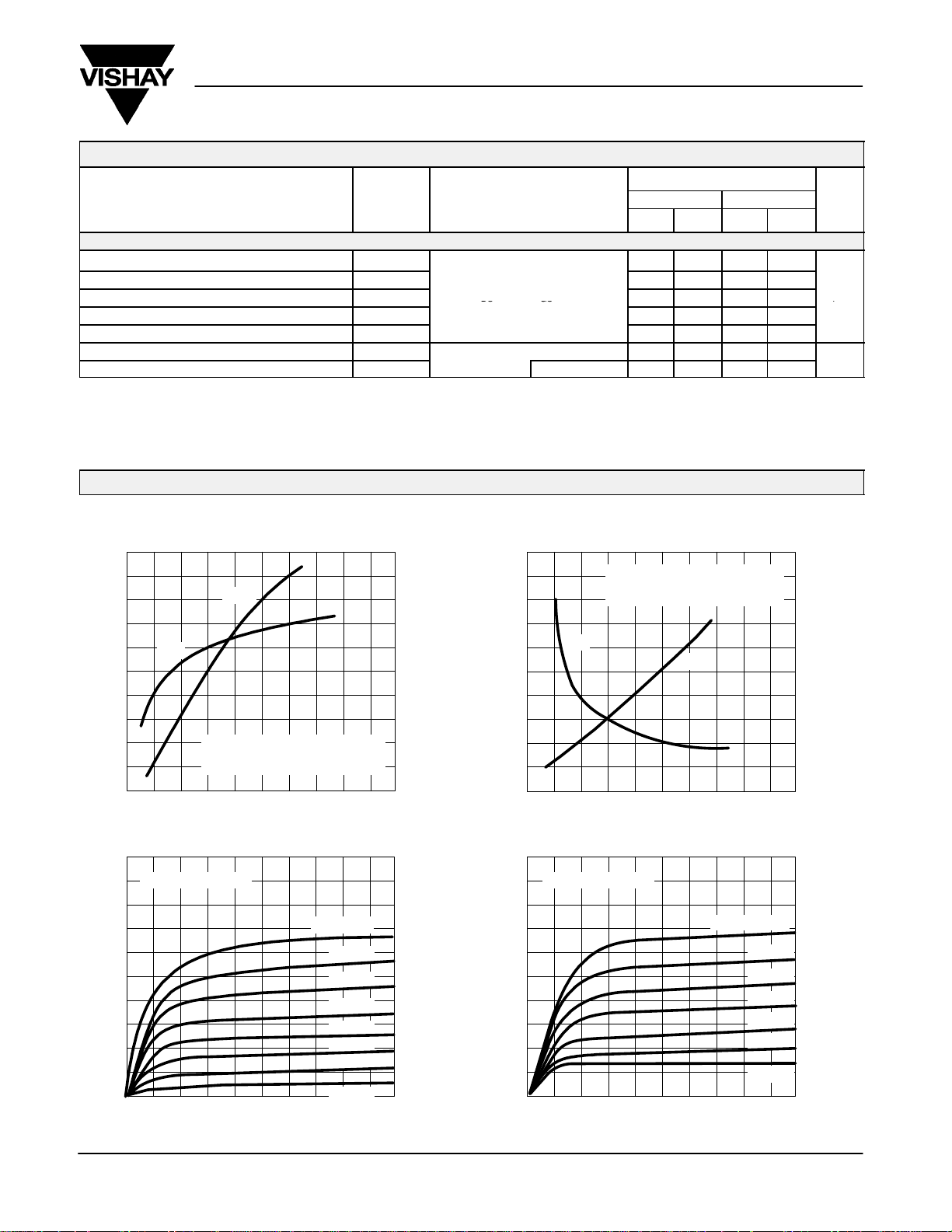
TYPICAL CHARACTERISTICS (TA = 25_C UNLESS OTHERWISE NOTED)
Drain Current and Transconductance
vs. Gate-Source Cutoff Voltage
20
I
16
12
g
fs
8
DSS
10
g
fs
− Forward Transconductance (mS)
8
6
4
On-Resistance and Output Conductance
vs. Gate-Source Cutoff Voltage
500
r
@ I
= 300 mA, V
DS
D
g
@ VDS = 10 V, VGS = 0 V
os
400
300
200
f = 1 kHz
r
DS
g
os
GS
= 0 V
100
80
60
40
gos − Output conductance (µS)
− Saturation Drain Current (mA)
4
DSS
I
0
0 −10−2 −4 −6 −8
10
8
6
4
− Drain Current (mA)
D
I
2
0
01024 68
Document Number: 70242
S-50147—Rev. H, 24-Jan-05
I
@ VDS = 10 V, VGS = 0 V
DSS
g
@ VDS = 10 V, VGS = 0 V
fs
f = 1 kHz
V
− Gate-Source Cutoff Voltage (V)
GS(off)
2
0
− Drain-Source On-Resistance ( Ω )
100
DS(on)
r
0
0 −10−2 −4 −6 −8
V
− Gate-Source Cutoff Voltage (V)
GS(off)
Output Characteristics Output Characteristics
15
V
= −2 V V
GS(off)
12
VGS = 0 V
−0.2 V
9
−0.4 V
−0.6 V
−0.8 V
−1.0 V
−1.2 V
−1.4 V
V
− Drain-Source Voltage (V) VDS − Drain-Source Voltage (V)
DS
6
− Drain Current (mA)
D
I
3
0
01024 68
GS(off)
= −3 V
20
0
VGS= 0 V
−0.3 V
−0.6 V
−0.9 V
−1.2 V
−1.5 V
−1.8 V
www.vishay.com
3

2N4416/2N4416A/SST4416
Vishay Siliconix
TYPICAL CHARACTERISTICS (TA = 25_C UNLESS OTHERWISE NOTED)
5
V
Output Characteristics
= −2 V
GS(off)
4
3
2
− Drain Current (mA)
D
I
1
0
0 1.0
0.2 0.4 0.6 0.8
V
− Drain-Source Voltage (V)
DS
VGS = 0 V
−0.2 V
−0.4 V
−0.6 V
−0.8 V
−1.0 V
−1.2 V
−1.4 V
5
V
4
3
2
− Drain Current (mA)
D
I
1
0
0 1.0
Output Characteristics
= −3 V
GS(off)
−0.6 V
−0.9 V
0.2 0.4 0.6 0.8
V
− Drain-Source Voltage (V)
DS
VGS = 0 V
−0.3 V
−1.2 V
−1.5 V
−1.8 V
−2.1 V
10
V
GS(off)
8
TA = −55_C
6
125_C
4
− Drain Current (mA)
D
I
2
0
0 −2−0.4 −0.8 −1.2 −1.6
Transconductance vs. Gate-Source Voltage
10
V
GS(off)
8
TA = −55_C
6
Transfer Characteristics
= −2 V
25_C
− Gate-Source Voltage (V)
V
GS
= −2 V
25_C
VDS = 10 V
VDS = 10 V
f = 1 kHz
10
V
= −3 V
GS(off)
8
TA = −55_C
6
4
− Drain Current (mA)
D
I
125_C
2
0
0 −3−0.6 −1.2 −1.8 −2.4
VGS − Gate-Source Voltage (V)
Transconductance vs. Gate-Source Voltgage
10
V
= −3 V
GS(off)
8
TA = −55_C
6
Transfer Characteristics
25_C
25_C
VDS = 10 V
VDS = 10 V
f = 1 kHz
4
2
− Forward Transconductance (mS)
fs
g
0
0 −2−0.4 −0.8 −1.2 −1.6
www.vishay.com
4
125_C
VGS − Gate-Source Voltage (V)
4
125_C
2
− Forward Transconductance (mS)
fs
g
0
0 −3−0.6 −1.2 −1.8 −2.4
VGS − Gate-Source Voltage (V)
Document Number: 70242
S-50147—Rev. H, 24-Jan-05

2N4416/2N4416A/SST4416
TYPICAL CHARACTERISTICS (TA = 25_C UNLESS OTHERWISE NOTED)
Vishay Siliconix
300
TA = 25_C
240
V
= −2 V
GS(off)
180
−3 V
120
− Drain-Source On-Resistance ( Ω )
60
DS(on)
r
0
0.1 1 10
ID − Drain Current (mA) ID − Drain Current (mA)
Common-Source Input Capacitance
vs. Gate-Source Voltage
5
f = 1 MHz
4
3
VDS = 0 V
2
On-Resistance vs. Drain Current Circuit Voltage Gain vs. Drain Current
100
80
60
40
− Voltage Gain
V
A
20
0
3
2.4
1.8
1.2
g
AV+
fsRL
1 ) RLg
os
Assume VDD = 15 V, VDS = 5 V
10 V
R
+
I
L
D
V
= −2 V
GS(off)
−3 V
1
Common-Source Reverse Feedback
Capacitance vs. Gate-Source Voltage
f = 1 MHz
VDS = 0 V
100.1
− Input Capacitance (pF)
iss
1
C
0
0 −20−4 −8 −12 −16
VGS − Gate-Source Voltage (V)
100
TA = 25_C
V
= 15 V
DS
V
= 0 V
GS
Common Source
10
(mS)
1
0.1
100 1000
Document Number: 70242
S-50147—Rev. H, 24-Jan-05
10 V
0.6
− Reverse Feedback Capacitance (pF)
rss
C
0
0 −20−4 −8 −12 −16
Input Admittance Forward Admittance
b
is
g
is
100
10
TA = 25_C
V
= 15 V
DS
V
= 0 V
GS
Common Source
(mS)
10 V
V
− Gate-Source Voltage (V)
GS
g
fs
−b
1
0.1
200 500 200 500
100 1000
f − Frequency (MHz) f − Frequency (MHz)
fs
www.vishay.com
5

2N4416/2N4416A/SST4416
Vishay Siliconix
TYPICAL CHARACTERISTICS (TA = 25_C UNLESS OTHERWISE NOTED)
10
TA = 25_C
V
V
Common Source
= 15 V
DS
GS
Reverse Admittance
= 0 V
10
−b
rs
Output Admittance
b
os
1
(mS)
0.1
0.01
100 1000
200 500
f − Frequency (MHz)
100 nA
10 nA
Gate Leakage Current
IG @ ID = 5 mA
1 mA
0.1 mA
1 nA
TA = 125_C
100 pA
5 mA
− Gate Leakage
10 pA
G
I
1 pA
TA = 25_C
0.1 mA
I
0.1 pA
012841620
VDG − Drain-Gate Voltage (V)
Equivalent Input Noise Voltage vs. Frequency Output Conductance vs. Drain Current
20
16
12
1 mA
GSS
−g
125_C
@ 25_C
V
= 10 V
DS
I
GSS
@
1
g
os
(mS)
rs
0.1
TA = 25_C
V
= 15 V
DS
V
= 0 V
GS
Common Source
0.01
100 1000
200 500
f − Frequency (MHz)
Common-Source Forward
Transconductance vs. Drain Current
10
V
= −3 V
GS(off)
8
6
25_C
4
2
− Forward Transconductance (mS)
fs
0
0.1 1 10
I
− Drain Current (mA)
D
20
V
= −3 V
GS(off)
16
TA = −55_C
12
VDS = 10 V
f = 1 kHz
TA = −55_C
125_C
VDS = 10 V
f = 1 kHz
25_C
en − Noise Voltage nV / Hz
8
4
V
= 0 V
GS
ID = 5 mA
0
10 100 1 k 100 k10 k
8
− Output Conductance (µS) g
os
g
4
125_C
0
0.1 1 10
− Drain Current (mA)f − Frequency (Hz)
I
D
Vishay Siliconix maintains worldw ide manufacturing capability. Products may be manufactured at one of several qualified locations. Reliability data for Silicon Technology and
Package Reliability represent a composite of all qualified locations. For related documents such as package/tape drawings, part marking, and reliability data, see
http://www.vishay.com/ppg?70242.
www.vishay.com
6
Document Number: 70242
S-50147—Rev. H, 24-Jan-05

 Loading...