

2N/PN/SST4117A Series
Vishay Siliconix
N-Channel JFETs
2N4117A PN4117A SST4117
2N4118A PN4118A SST4118
2N4119A PN4119A SST4119
PRODUCT SUMMARY
Part Number V
4117 −0.6 to −1.8 −40 70 30
4118 −1 to −3 −40 80 80
4119 −2 to −6 −40 100 200
FEATURES BENEFITS APPLICATIONS
D Ultra-Low Leakage: 0.2 pA
D Very Low Current/Voltage Operation
D Ultrahigh Input Impedance
D Low Noise
GS(off)
(V) V
(BR)GSS
Min (V) gfs Min (mS)
I
DSS
Min (mA)
D Insignificant Signal Loss/Error Voltage
with High-Impedance Source
D Low Power Consumption (Battery)
D Maximum Signal Output, Low Noise
D High Sensitivity to Low-Level Signals
D High-Impedance Transducer
Amplifiers
D Smoke Detector Input
D Infrared Detector Amplifier
D Precision Test Equipment
DESCRIPTION
The 2N/PN/SST4117A series of n-channel JFETs provide
ultra-high input impedance. These devices are specified with
a 1-pA limit and typically operate at 0.2 pA. This makes them
perfect choices for use as high-impedance sensitive front-end
amplifiers.
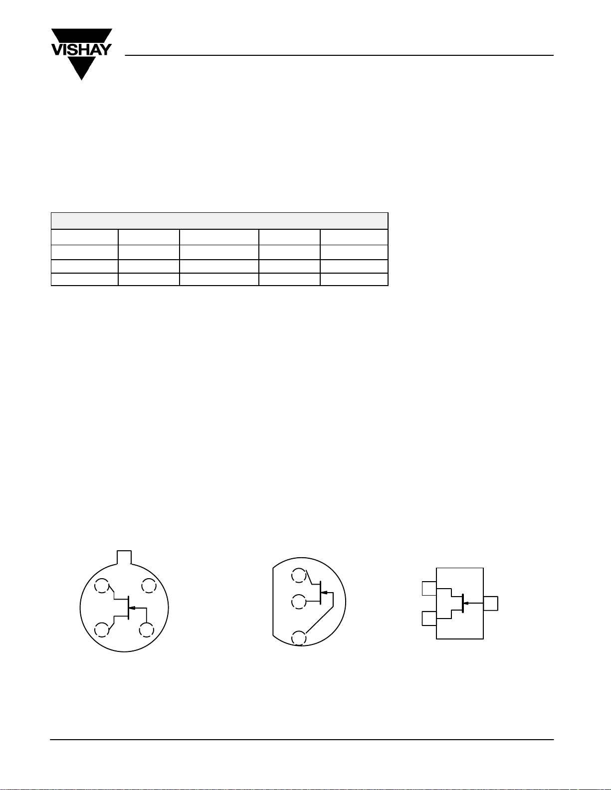
TO-206AF
(TO-72)
S
1
23
D
Top View
2N4117A
2N4118A
2N4119A
C
4
G
D
S
G
TO-226AA
(TO-92)
1
2
3
Top View
PN4117A
PN4118A
PN4119A
The hermetically sealed TO-206AF package allows full
military processing per MIL-S-19500 (see Military
Information). The TO-226A (TO-92) plastic package provides
a low-cost option. The TO-236 (SOT-23) package provides
surface-mount capability. Both the PN and SST series are
available in tape-and-reel for automated assembly (see
Packaging Information).
TO-236
(SOT-23)
1
D
G
3
S
2
Top View
SST4117 (T7)*
SST4118 (T8)*
SST4119 (T9)*
*Marking Code for TO-236
For applications information see AN105.
Document Number: 70239
S-41231—Rev. G, 28-Jun-04
www.vishay.com
1
2N/PN/SST4117A Series
V
VGS = −10 V
S
VDS = 10 V, VGS = 0 V
Common-Source
Common-Source
f = 1 MHz
Vishay Siliconix
ABSOLUTE MAXIMUM RATINGS
Gate-Source/Gate-Drain Voltage −40V. . . . . . . . . . . . . . . . . . . . . . . . . . . . . . . .
Forward Gate Current 50 mA. . . . . . . . . . . . . . . . . . . . . . . . . . . . . . . . . . . . . . . . .
Lead Temperature (
Power Dissipation (case 25_C) :
Storage Temperature : (2N Prefix) −65 to 175_C. . . . . . . . . . . . . . . . . . .
(PN, SST Prefix) −55 to 150_C. . . . . . . . . . . . .
Operating Junction Temperature :
(2N Prefix) −55 to 175_C. . . . . . . . . . . . . . . . . . .
(PN, SST Prefix) −55 to 150_C. . . . . . . . . . . . .
Notes
a. Derate 2 mW/_C above 25_C
b. Derate 2.8 mW/_C above 25_C
SPECIFICATIONS (TA = 25_C UNLESS OTHERWISE NOTED)
Parameter Symbol Test Conditions TypaMin Max Min Max Min Max Unit
Static
Gate-Source
Breakdown Voltage
Gate-Source Cutoff Voltage V
Saturation Drain Current I
Gate Reverse Current I
Gate Operating Current
Drain Cutoff Current
Gate-Source Forward Voltage
b
b
b
Dynamic
Common-Source
Forward Transconductance
Common-Source
Output Conductance
Common-Source
Input Capacitance
Common-Source
Reverse Transfer Capacitance
Equivalent Input Noise Voltage
Notes
a. Typical values are for DESIGN AID ONLY, not guaranteed nor subject to production testing. NT
b. This parameter not registered with JEDEC.
b
V
(BR)GSS
GS(off)
DSS
GSS
I
D(off)
V
GS(F)
g
g
C
C
e
IG = −1 mA , VDS = 0 V
VDS = 10 V, ID = 1 nA
VDS = 10 V, VGS = 0 V
VGS = −20 V
V
= 0 V
DS
VGS = −20 V
V
= 0 V
DS
= 150_C
T
A
VGS = −10 V
VDS = 0 V
VGS = −10 V
V
= 0 V
DS
= 100_C
T
A
I
G
VDG = 15 V, ID = 30 mA
2N
PN −0.2 −1 −1 −1
SST −0.2 −10 −10 −10
PN/SST −0.03 −2.5 −2.5 −2.5 nA
VDS = 10 V, VGS = −8 V 0.2
IG = 1 mA , VDS = 0 V 0.7 V
fs
os
V
= 10 V, VGS = 0 V
D
f = 1 kHz
2N/PN 1.2 3 3 3
iss
rss
n
VDS = 10 V
VGS = 0 V
f = 1 MHz
VDS = 10 V, VGS = 0 V
f = 1 kHz
SST 1.2
2N/PN 0.3 1.5 1.5 1.5
SST 0.3
1
/16” from case for 10 sec.) 300_C. . . . . . . . . . . . . . . . . . .
(2N Prefix)
(PN, SST Prefix)
a
b
300 mW. . . . . . . . . . . . . . . . . . . . . .
350 mW. . . . . . . . . . . . . . . .
Limits
4117 4118 4119
−70
−40 −40 −40
−0.6 −1.8 −1 −3 −2 −6
90
30
−0.2 −1 −1 −1 pA
−0.4 −2.5 −2.5 −2.5 nA
−0.2
210
70
3 5 10
15
240
80
200
600
mA
pA
pA
250
80
100
330
mS
pF
nV⁄
√Hz
V
www.vishay.com
2
Document Number: 70239
S-41231—Rev. G, 28-Jun-04

2N/PN/SST4117A Series
TYPICAL CHARACTERISTICS (TA = 25_C UNLESS OTHERWISE NOTED)
Vishay Siliconix
− Saturation Drain Current (µA)
DSS
I
1000
800
600
400
200
15
12
Drain Current and Transconductance
vs. Gate-Source Cutoff Voltage
I
@ VDS = 10 V, VGS = 0 V
DSS
g
@ VDS = 10 V, VGS = 0 V
fs
f = 1 kHz
g
fs
0
0 −5−4−3−2−1
V
− Gate-Source Cutoff Voltage (V)
GS(off)
On-Resistance and Output Conductance
vs. Gate-Source Cutoff Voltage
r
DS
9
6
300
240
1 nA
g
fs
− Forward Transconductance (µS)
V
100 pA
Gate Leakage Current
= −2.5 V
GS(off)
TA = 125_C
10 mA
I
GSS
100 mA
@ 125_C
180
100 mA
10 mA
I
DSS
120
60
10 pA
− Gate Leakage
G
I
1 pA
I
GSS
@ 25_C
TA = 25_C
0
0.1 pA
06 30
12 18 24
VDG − Drain-Gate Voltage (V)
Common-Source Forward Transconductance
5
g
os
g
os
4
− Output Conductance (µS)
200
160
V
GS(off)
TA = −55_C
3
2
120
80
vs. Drain Current
= −2.5 V
25_C
125_C
− Drain-Source On-Resistance (kW)
3
DS(on)
r
0
0 −3 −5−4−2−1
− Gate-Source Cutoff Voltage (V)
GS(off)
Output Characteristics
100
V
= −0.7 V V
GS(off)
80
60
− Drain Current (µA)
D
I
20
0
0168420
VDS − Drain-Source Voltage (V)
Document Number: 70239
S-41231—Rev. G, 28-Jun-04
rDS @ ID = 10 mA, VGS = 0 V
g
@ VDS = 10 V, VGS = 0 V
os
f = 1 kHz
VGS = 0 V
12 0 16842012
−0.1 V
−0.2 V
−0.3 V
−0.4 V
−0.5 V
1
0
40
− Forward Transconductance (µS)
fs
g
VDS = 10 V
f = 1 kHz
0
0.01 0.1 1
− Drain Current (mA)V
I
D
Output Characteristics
500
= −2.5 V
GS(off)
400
VGS = 0 V
300
−0.5 V
20040
−1.0 V
− Drain Current (µA)
D
I
100
−1.5 V
−2.0 V
0
V
− Drain-Source Voltage (V)
DS
www.vishay.com
3

2N/PN/SST4117A Series
Vishay Siliconix
TYPICAL CHARACTERISTICS (TA = 25_C UNLESS OTHERWISE NOTED)
100
V
= −0.7 V V
GS(off)
80
60
TA = 125_C
40
− Drain Current (µA)
D
25_C
20
−55_C
0
0 −0.4−0.2 −0.8 −1.0
− Gate-Source Voltage (V)
V
GS
−0.6 0 −0.4−0.2 −0.8 −1.0−0.6
500
V
= −2.5 V V
GS(off)
400
TA = −55_C
300
25_C
Transconductance vs. Gate-Source VoltageTransfer Characteristics
200
VDS = 10 V VDS = 10 V
160
= −0.7 V
GS(off)
TA = −55_C
f = 1 kHz
25_C
120
80
40
− Forward Transconductance (µS)
fs
125_C
0
− Gate-Source Voltage (V)
V
GS
Transconductance vs. Gate-Source VoltageTransfer Characteristics
300
VDS = 10 V VDS = 10 V
GS(off)
= −2.5 V
f = 1 kHz
240
TA = −55_C
180
25_C
200
− Drain Current (µA) I
D
I
100
0
100
80
60
40
− Voltage Gain
V
A
20
0
125_C
0 −4 −5−2−1
V
− Gate-Source Voltage (V) VGS − Gate-Source Voltage (V)
GS
−30−4 −5−2−1 −3
Circuit Voltage Gain vs. Drain Current
g
AV+
Assume VDD = 15 V, VDS = 5 V
RL+
fsRL
1 ) RLg
10 V
I
D
V
= −0.7 V
GS(off)
I
− Drain Current (mA)
D
os
−2.5 V
0.1 10.01
120
125_C
− Forward Transconductance (µS) g
60
fs
g
0
Common-Source Input Capacitance
vs. Gate-Source Voltage
2.0
f = 1 MHz
1.6
1.2
0.8
− Input Capacitance (pF)
iss
C
0.4
0
0 −16 −20−8−4 −12
VDS = 0 V
V
GS
10 V
− Gate-Source Voltage (V)
www.vishay.com
4
Document Number: 70239
S-41231—Rev. G, 28-Jun-04

2N/PN/SST4117A Series
TYPICAL CHARACTERISTICS (TA = 25_C UNLESS OTHERWISE NOTED)
Vishay Siliconix
Common-Source Reverse Feedback Capacitance
0.5
0.4
0.3
0.2
0.1
− Reverse Feedback Capacitance (pF)
rss
C
0
0 −8 −20−16−4
2
1
− Output Conductance (µS)
os
g
0
0.01 0.1 1
vs. Gate-Source Voltage
f = 1 MHz
VDS = 0 V
10 V
− Gate-Source Voltage (V) f − Frequency (Hz)
V
GS
V
= −2.5 V
GS(off)
TA = −55_C
125_C
− Drain Current (mA)
I
D
−12
25_C
VDS = 10 V
f = 1 kHz
Equivalent Input Noise Voltage vs. Frequency
200
VDS = 10 V
160
120
80
40
en − Noise Voltage nV / Hz
0
10 100 1 k
ID = 10 mA
VGS = 0 V
On-Resistance vs. Drain CurrentOutput Conductance vs. Drain Current
20
16
12
8
− Drain-Source On-Resistance ( Ω )
4
DS(on)
r
TA = 25_C
0
0.01 0.1 1
V
= −0.7 V
GS(off)
ID − Drain Current (mA)
10 k
100 k
−2.5 V
Document Number: 70239
S-41231—Rev. G, 28-Jun-04
www.vishay.com
5

 Loading...