

Bulletin I2117 rev. D 12/98
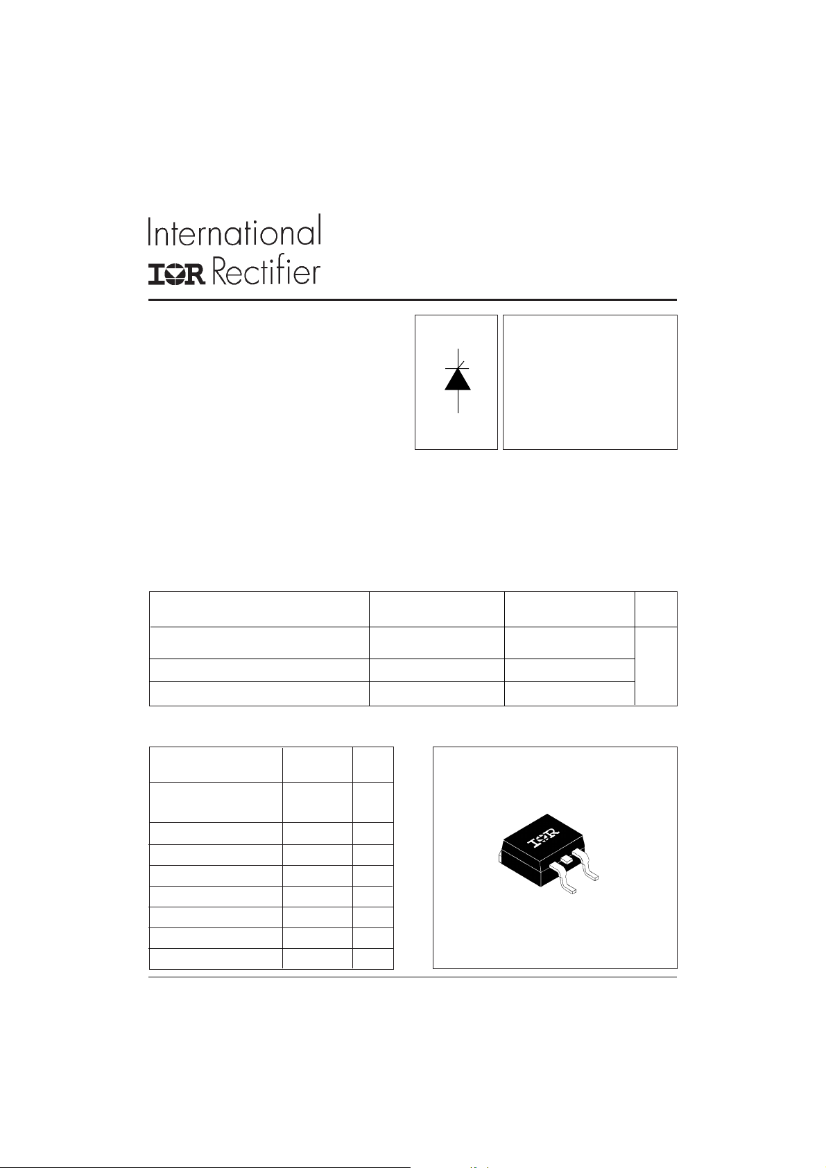
SAFE
IR
Series
25TTS..S
SURFACE MOUNTABLE
PHASE CONTROL SCR
Description/Features
The 25TTS..S SAFEIR series of silicon controlled
rectifiers are specifically designed for medium
power switching and phase control applications.
The glass passivation technology used has reliable operation up to 125° C junction temperature.
Typical applications are in input rectification (soft
start) and these products are designed to be used
with International Rectifier input diodes, switches
and output rectifiers which are available in identical
package outlines.
Output Current in Typical Applications
Applications Single-phase Bridge Three-phase Bridge Units
NEMA FR-4 or G10 glass fabric-based epoxy
with 4 oz (140µm) copper
Aluminum IMS, R
Aluminum IMS with heatsink, R
TA = 55°C, TJ = 125°C, footprint 300mm
= 15°C/W 8.5 13.5 A
thCA
= 5°C/W 16.5 25.0
thCA
2
Major Ratings and Characteristics
3.5 5.5
V
I
TSM
V
< 1.25V @ 16A
T
= 300A
800 to 1600V
RRM
Characteristics 25TTS..S Units
I
Sinusoidal 16 A
T(AV)
waveform
I
RMS
V
V
/
RRM
DRM
I
TSM
V
@ 16 A, TJ = 25°C 1.25 V
T
dv/dt 500 V/µs
di/dt 150 A/µs
T
J
25 A
up to 1600 V
300 A
- 40 to 125 °C
www.irf.com
D2 PAK (SMD-220)
1
25TTS..S SAFEIR Series
Bulletin I2117 rev. D 12/98
Voltage Ratings
V
, maximum V
RRM
Part Number
peak reverse voltage peak direct voltage 125°C
VVmA
25TTS08S 800 800 10
25TTS12S 1200 1200
25TTS16S 1600 1600
Absolute Maximum Ratings
Parameters 25TTS..S Units Conditions
I
Max. Average On-state Current 16 A @ TC = 93° C, 180° conduction half sine wave
T(AV)
I
Max. RMS On-state Current 25
RMS
I
Max. Peak One Cycle Non-Repetitive 30 0 10ms Sine pulse, rated V
TSM
Surge Current 350 10ms Sine pulse, no voltage reapplied
I2t Max. I2t for fusing 450 A2s 10ms Sine pulse, rated V
630 10ms Sine pulse, no voltage reapplied
2
I
√t Max. I2√t for fusing 6300 A2√s t = 0.1 to 10ms, no voltage reapplied
VTMMax. On-state Voltage Drop 1.25 V @ 16A, TJ = 25°C
r
On-state slope resistance 12.0 mΩ T
t
V
Threshold Voltage 1.0 V
T(TO)
IRM/IDMMax.Reverse and Direct 0.5 mA TJ = 25 °C
Leakage Current 10 TJ = 125 °C
I
Holding Current Typ. Max. Anode Supply = 6V, Resistive load, Initial IT=1A
H
-- 100 mA 25TTS08S, 25TTS12S
100 150 25TTS16S
IL Max. Latching Current 200 mA Anode Supply = 6V, Resistive load
dv/dt Max. Rate of Rise of off-state Voltage 500 V/µs
di/dt Max. Rate of Rise of turned-on Current 15 0 A/µs
= 125°C
J
, maximum I
DRM
applied
RRM
applied
RRM
VR = rated V
RRM
/ V
RRM/IDRM
DRM
2
www.irf.com
25TTS..S SAFEIR Series
Bulletin I2117 rev. D 12/98
Triggering
Parameters 25TTS..S Units Conditions
PGMMax. peak Gate Power 8.0 W
P
Max. average Gate Power 2.0
G(AV)
+ I
Max. paek positive Gate Current 1.5 A
GM
Max. paek negative Gate Voltage 10 V
- V
GM
IGTMax. required DC Gate Current 60 mA Anode supply = 6V, resistive load, TJ = - 10°C
to trigger 45 Anode supply = 6V, resistive load, TJ = 25°C
20 Anode supply = 6V, resistive load, T
Max. required DC Gate Voltage 2.5 V Anode supply = 6V, resistive load, TJ = - 10°C
V
GT
to trigger 2.0 Anode supply = 6V, resistive load, T
1.0 Anode supply = 6V, resistive load, TJ = 125°C
Max. DC Gate Voltage not to trigger 0.25 TJ = 125°C, V
V
GD
IGDMax. DC Gate Current not to trigger 2.0 mA TJ = 125°C, V
= rated value
DRM
= rated value
DRM
Switching
= 125°C
J
= 25°C
J
Parameters 25TTS..S Units Conditions
t
Typical turn-on time 0.9 µs TJ = 25°C
gt
t
Typical reverse recovery time 4 TJ = 125°C
rr
t
Typical turn-off time 110
q
Thermal-Mechanical Specifications
Parameters 25TTS..S Units Conditions
TJMax. Junction Temperature Range - 40 to 125 °C
T
Max. Storage Temperature Range - 40 to 125 °C
stg
Soldering Temperature 240 °C for 10 seconds (1.6mm from case)
R
Max. Thermal Resistance Junction 1.1 °C/W D C operation
thJC
to Case
R
Typ. Thermal Resistance Junction 40 °C/W
thJA
to Ambient (PCB Mount)**
wt Approximate Weight 2 (0.07) g (oz.)
2
T Case Style D
**When mounted on 1" square (650mm2) PCB of FR-4 or G-10 material 4 oz (140µm) copper 40°C/W
For recommended footprint and soldering techniques refer to application note #AN-994
www.irf.com
Pak (SMD-220)
3

25TTS..S SAFEIR Series
Bulletin I2117 rev. D 12/98
130
120
110
100
90
Maximum Allowable Case Temperature (°C)
0 5 10 15 20
25TTS.. Series
R (DC) = 1.1 °C/W
thJC
Conduction Angle
30°
60°
90°
120°
180°
Averag e On-s tate Curr en t (A)
Fig. 1 - Current Rating Characteristics
25
180°
120°
20
15
10
Maximum Average On-state Powe r Loss (W)
90°
60°
30°
RMS Limit
Conduction Angle
5
0
048121620
Average On-state Current (A)
25TTS.. Series
T = 125°C
J
Fig. 3 - On-state Power Loss Characteristics
130
120
110
100
90
80
Max imum Allowable Case Temp erat u re (°C)
0 5 10 15 20 25 30
25TTS.. Series
R (DC) = 1.1 °C/W
thJC
Conduction Period
90°
120°
60°
30°
Average On-state Current (A)
180°
DC
Fig. 2 - Current Rating Characteristics
35
DC
180°
30
120°
90°
25
60°
30°
20
RMS Lim it
15
10
5
0
Maximum Averag e On-state Power Loss (W)
0 5 10 15 20 25 30
Average On-state Current (A)
Conduction Period
25TTS.. Series
T = 125°C
J
Fig. 4 - On-state Power Loss Characteristics
350
At Any Rated L oad Con ditio n A nd With
Rated V Applied Following Surge.
RRM
300
250
200
25TTS.. Series
Peak Half Sine Wave On-state Current (A)
150
1 10 100
Number Of Equal Amplitude Half Cycle Current Pulses (N)
Initial T = 125°C
J
@ 60 Hz 0.00 83 s
@ 50 Hz 0.01 00 s
Fig. 5 - Maximum Non-Repetitive Surge Current
4
400
Maximum Non Repe titive Surge Current
Versus Pulse Train Du ration. Control
Of C on d uc tion Ma y Not Be Mai n ta ined.
350
300
250
200
150
25TTS.. Se ri es
Pea k Half Sine Wave On-sta te Cu rrent (A)
100
0.01 0.1 1
Pulse Train Duration (s)
Initial T = 125°C
No Voltage Reapplied
Rated V Reapplied
J
RRM
Fig. 6 - Maximum Non-Repetitive Surge Current
www.irf.com

1000
100
25TTS..S SAFEIR Series
Bulletin I2117 rev. D 12/98
T = 25°C
J
10
T = 125°C
J
www.irf.com
Instantaneous On-state Current (A)
1
012345
25TTS.. Series
Ins ta n ta n e ou s On-sta te Voltage (V)
Fig. 7 - On-state Voltage Drop Characteristics
10
thJC
1
D = 0.50
D = 0.33
D = 0.25
D = 0.17
D = 0.08
0.1
Single Pulse
Trans ient Thermal Impedance Z (°C/W)
0.01
0.0001 0.001 0.01 0.1 1 10
Square Wave Pulse Duration (s)
Steady State Value
(DC Oper ation )
25TTS.. Series
Fig. 8 - Gate Characteristics
100
Rectangular gate pulse
a)Recommended load line for
rated di/dt: 10 V, 20 ohms
tr = 0.5 µs, tp >= 6 µs
b)Recommended load line for
<= 30% rated di/dt: 10 V, 65 ohms
10
tr = 1 µs, tp >= 6 µs
TJ = 25 °C
1
VGD
Instantaneous Gate Voltage (V)
IGD
0.1
0.001 0.01 0.1 1 10 100
TJ = 125 °C
25TTS. . Se r ies
Inst antaneous Gate Current (A)
Fig. 9 - Thermal Impedance Z
(a)
(b)
TJ = -10 °C
thJC
(1) PGM = 40 W, tp = 1 ms
(2) PGM = 20 W, tp = 2 ms
(3 ) PGM = 8 W, tp = 5 ms
(4) PGM = 4 W, tp = 10 ms
(3) (2) (1)
(4)
Frequency Limited by PG(AV)
Characteristics
5

25TTS..S SAFEIR Series
Bulletin I2117 rev. D 12/98
Marking Information
EXAMPLE: THIS IS AN 25TTS16S
Tape & Reel Information
TRR
4.10 (0.161)
3.90 (0.153)
F E E D DIRECTION
TRL
1.85 (0.073)
1.65 (0.065)
10.90 (0.429)
10.70 (0.421)
INTERNATIONAL
RECTIFIER LOGO
ASSEMBLY
LOT CODE
1.60 (0.063)
1.50 (0.059)
16.10 (0.634)
15.90 (0.626)
9G3A
1.60 (0.063)
1.50 (0.059)
11.60 (0.457)
11.40 (0.449)
1.75 (0.069)
1.25 (0.049)
(A)
25TTS16S
9512
(K) (G)
DIA.
15.42 (0.609)
15.22 (0.601)
DIA.
PART NUMBER
DATE CODE (YYWW)
YY = YEAR
WW = WEEK
0.368 (0.0145)
0.342 (0.0135)
24.30 (0.957)
23.90 (0.941)
4.72 (0.186)
4.52 (0.178)
FEED DI RECTI ON
360 (14.173)
DIA. MAX.
6
13.50 (0.532)
12.80 (0.504)
DIA.
Dimensions in millimeters and inches
26.40 (1.039)
24.40 (0.961)
60 (2.3 62)
DIA. MIN.
SMD-220 Tape & Reel
When ordering, indica te the part
number, part orientation, and the
quantity. Quantities are in multiples
of 800 pieces per reel for both
TRL and TRR.
www.irf.com

Outline Table
10.16 (0.40)
1.40 (0.055)
3X
1.14 (0.045)
93°
15.49 (0.61)
14.73 (0.58)
1 (K) Cathode
2 (A) Anode
3 (G) Gate
Dimensions in millimeters and inches
REF.
(K) (G)
13
2
(A)
2.61 (0.10)
2.32 (0.09)
8.89 (0.35)
REF.
0.93 (0.37)
2X
0.69 (0.27)
5.08 (0 .20) REF.
6.47 (0.25)
6.18 (0.24)
4.57 (0.18)
4.32 (0.17)
0.61 (0.02) M AX.
25TTS..S SAFEIR Series
Bulletin I2117 rev. D 12/98
4.69 (0.18)
4.20 (0.16)
1.32 (0.05)
1.22 (0.05)
5.28 (0.21)
4.78 (0.19)
0.55 (0.02)
0.46 (0.02)
MINIMUM RECOMMENDED FOOTPRINT
11.43 (0.45)
8.89 (0.35)
17.78 (0.70)
3.81 (0.15)
2.08 (0.08)
2X
2.54 (0.10)
2X
Ordering Information Table
Device Code
25 T T S 16 S TRL
1
1 - Current Rating, RMS value
2 - Circuit Configuration
T = Single Thyristor
3 - Package
T = TO-220AC
4 - Type of Silicon
S = Converter Grade
5 - Voltage code: Code x 100 = V
6 - S = TO-220 D2Pak (SMD 220) Version
7 - Tape and Reel Option
TRL = Left Reel
TRR = Right Orientation Reel
www.irf.com
3
RRM
524
6
7
08 = 800V
12 = 1200V
16 = 1600V
(A)
1 (K)
2
(G) 3
7

25TTS..S SAFEIR Series
Bulletin I2117 rev. D 12/98
WORLD HEADQUARTERS: 233 Kansas St., El Segundo, California 90245 U.S.A. Tel: (310) 322 3331. Fax: (310) 322 3332.
EUROPEAN HEADQUARTERS: Hurst Green, Oxted, Surrey RH8 9BB, U.K. Tel: ++ 44 1883 732020. Fax: ++ 44 1883 733408.
IR SOUTHEAST ASIA: 1 Kim Seng Promenade, Great World City West Tower,13-11, Singapore 237994. Tel: ++ 65 838 4630.
http://www.irf.com Fax-On-Demand: +44 1883 733420 Data and specifications subject to change without notice.
8
IR CANADA: 15 Lincoln Court, Brampton, Markham, Ontario L6T3Z2. Tel: (905) 453 2200. Fax: (905) 475 8801.
IR GERMANY: Saalburgstrasse 157, 61350 Bad Homburg. Tel: ++ 49 6172 96590. Fax: ++ 49 6172 965933.
IR ITALY: Via Liguria 49, 10071 Borgaro, Torino. Tel: ++ 39 11 4510111. Fax: ++ 39 11 4510220.
IR FAR EAST: K&H Bldg., 2F, 30-4 Nishi-Ikebukuro 3-Chome, Toshima-Ku, Tokyo, Japan 171. Tel: 81 3 3983 0086.
IR TAIWAN: 16 Fl. Suite D.207, Sec. 2, Tun Haw South Road, Taipei, 10673, Taiwan. Tel: 886 2 2377 9936.
www.irf.com
 Loading...