

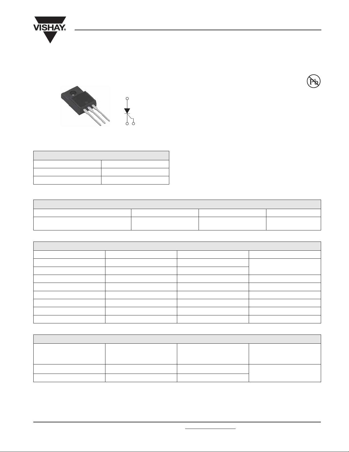
TO-220AB FULL-PAK
PRODUCT SUMMARY
VT at 16 A < 1.25 V
I
TSM
V
RRM
25TTS...FPPbF High Voltage Series
Vishay High Power Products
Phase Control SCR
TO-220AB FULL-PAK, 25 A
DESCRIPTION/FEATURES
2
(A)
1 (K)
(G) 3
200 A
800/1200 V
The 25TTS...FPPbF High Voltage Series of
silicon controlled rectifiers are specifically
designed for medium power switching and phase
control applications. The glass passivation
technology used has reliable operation up to 140 °C junction
temperature.
Typical applications are in input rectification (soft start) and
these products are designed to be used with Vishay HPP
input diodes, switches and output rectifiers which are
available in identical package outlines. Fully isolated
package (V
= 2500 V
INS
This product has been designed and qualified for industrial
level and lead (Pb)-free (“PbF” suffix).
); plastic material 94VRo.
RMS
Available
RoHS*
COMPLIANT
OUTPUT CURRENT IN TYPICAL APPLICATIONS
APPLICATIONS SINGLE-PHASE BRIDGE THREE-PHASE BRIDGE UNITS
Capacitive input filter T
common heatsink of 1 °C/W
= 55 °C, TJ = 125 °C,
A
18 22 A
MAJOR RATINGS AND CHARACTERISTICS
PARAMETER TEST CONDITIONS VALUES UNITS
I
T(AV)
I
RMS
V
RRM/VDRM
I
TSM
V
T
dV/dt 500 V/µs
dI/dt 150 A/µs
T
J
Sinusoidal waveform 16
25
800/1200 V
300 A
16 A, TJ = 25 °C 1.25 V
- 40 to 125 °C
A
VOLTAGE RATINGS
, MAXIMUM PEAK
V
RRM
PART NUMBER
25TTS08FPPbF 800 800
25TTS12FPPbF 1200 1200
REVERSE VOLTAGE
V
V
, MAXIMUM PEAK
DRM
DIRECT VOLTAGE
V
I
RRM/IDRM
AT 125 °C
mA
10
* Pb containing terminations are not RoHS compliant, exemptions may apply
Document Number: 94384 For technical questions, contact: diodes-tech@vishay.com
Revision: 27-May-08 1
www.vishay.com
25TTS...FPPbF High Voltage Series
Vishay High Power Products
Phase Control SCR
TO-220AB FULL-PAK, 25 A
ABSOLUTE MAXIMUM RATINGS
PARAMETER SYMBOL TEST CONDITIONS
Maximum average on-state current I
Maximum RMS on-state current I
Maximum peak, one-cycle,
non-repetitive surge current
2
Maximum I
Maximum I
t for fusing I2t
2
√t for fusing I2√t t = 0.1 to 10 ms, no voltage reapplied 6300 A2√s
Maximum on-state voltage drop V
On-state slope resistance r
Threshold voltage V
Maximum reverse and direct leakage current I
RM/IDM
Holding current I
Maximum latching current I
T(AV)
RMS
I
TSM
TM
T(TO)
H
L
t
TC = 85 °C, 180° conduction half sine wave 16
25
10 ms sine pulse, rated V
applied 300
RRM
10 ms sine pulse, no voltage reapplied 350
10 ms sine pulse, rated V
applied 450
RRM
10 ms sine pulse, no voltage reapplied 630
16 A, TJ = 25 °C 1.25 V
TJ = 125 °C
TJ = 25 °C
= 125 °C 10
T
J
V
= Rated V
R
RRM/VDRM
Anode supply = 6 V, resistive load, initial IT = 1 A - 100
Anode supply = 6 V, resistive load 200
Maximum rate of rise of off-state voltage dV/dt 500 V/µs
Maximum rate of rise of turned-on current dI/dt 150 A/µs
VALUES
TYP. MAX.
12.0 mΩ
1.0 V
0.5
UNITS
A
2
A
s
mA
TRIGGERING
PARAMETER SYMBOL TEST CONDITIONS VALUES UNITS
Maximum peak gate power P
Maximum average gate power P
Maximum peak positive gate current + I
Maximum peak negative gate voltage - V
GM
G(AV)
GM
GM
8.0
2.0
1.5 A
10 V
W
Anode supply = 6 V, resistive load, TJ = - 10 °C 60
Maximum required DC gate current to trigger I
GT
Anode supply = 6 V, resistive load, T
= 25 °C 45
J
= 125 °C 20
J
mAAnode supply = 6 V, resistive load, T
Anode supply = 6 V, resistive load, TJ = - 10 °C 2.5
Maximum required DC gate
voltage to trigger
Maximum DC gate voltage not to trigger V
Maximum DC gate current not to trigger I
V
GT
GD
GD
Anode supply = 6 V, resistive load, T
Anode supply = 6 V, resistive load, T
TJ = 125 °C, V
= Rated value
DRM
= 25 °C 2.0
J
= 125 °C 1.0
J
V
0.25
2.0 mA
SWITCHING
PARAMETER SYMBOL TEST CONDITIONS VALUES UNITS
Typical turn-on time t
Typical turn-off time t
gt
rr
q
TJ = 25 °C 0.9
TJ = 125 °C
110
4
µsTypical reverse recovery time t
www.vishay.com For technical questions, contact: diodes-tech@vishay.com
Document Number: 94384
2 Revision: 27-May-08
25TTS...FPPbF High Voltage Series
Phase Control SCR
Vishay High Power Products
TO-220AB FULL-PAK, 25 A
THERMAL AND MECHANICAL SPECIFICATIONS
PARAMETER SYMBOL TEST CONDITIONS VALUES UNITS
Maximum junction and storage
temperature range
Maximum thermal resistance,
junction to case
Maximum thermal resistance,
junction to ambient
Typical thermal resistance,
case to heatsink
Approximate weight
Mounting torque
Marking device Case style TO-220AB FULL-PAK (94/V0)
minimum 6 (5)
maximum 12 (10)
T
, T
J
Stg
R
thJC
R
thJA
R
thCS
DC operation 1.5
Mounting surface, smooth and greased 1.5
- 40 to 125 °C
62
2g
0.07 oz.
25TTS08FP
25TTS12FP
°C/W
kgf · cm
(lbf · in)
Document Number: 94384 For technical questions, contact: diodes-tech@vishay.com
Revision: 27-May-08 3
www.vishay.com

25TTS...FPPbF High Voltage Series
Vishay High Power Products
130
120
110
100
90
30°
80
70
Maximum Allowable Case Temperature (°C)
0 5 10 15 20
Average On-state Current (A)
Fig. 1 - Current Rating Characteristics
130
120
110
100
25TTS.. Se rie s
R ( DC) = 1. 5 °C/ W
thJC
Conduc tion Angle
60°
90°
120°
180°
25TTS.. Series
R ( DC) = 1.5 °C/ W
thJC
Conduc tion Period
Phase Control SCR
TO-220AB FULL-PAK, 25 A
35
30
25
20
15
10
Maximum Average On-state Power Loss (W)
350
300
250
DC
180°
120°
90°
60°
30°
RM S Lim it
Conduc tion Period
5
0
0 5 10 15 20 25 30
Avera ge On-state Current (A)
2 5 TTS. . Se r i e s
T = 125°C
J
Fig. 4 - On-State Power Loss Characteristics
At Any Rated Load Condition And With
Rated V Applied Following Surge.
RRM
Init ial T = 125°C
J
@ 6 0 Hz 0. 00 83 s
@ 5 0 Hz 0. 01 00 s
90
30°
60°
80
70
Maximum Allo wable Case Temperature (°C)
0 5 10 15 20 25 30
90°
120°
180°
DC
Average On-state Current (A)
Fig. 2 - Current Rating Characteristics
25
20
15
10
Maximum Average On-state Powe r Loss (W)
180°
120°
90°
60°
30°
RM S Lim i t
Conduct ion Angle
5
0
048121620
Average On-state Current (A)
25TTS. . Se r i e s
T = 125°C
J
ine Wa ve On-st a te Current (A)
200
25TTS. . Se ri e s
Pe a k H a l f S
150
110100
Number Of Equal Amplitude Half Cycle Current Pulses (N)
Fig. 5 - Maximum Non-Repetitive Surge Current
400
Ma ximum Non Rep e titive Surg e Curre nt
Versus Pulse Train Durat ion. Contro l
Of Cond uc tion Ma y Not Be Maintained.
350
300
250
200
ine Wave On-sta te Current (A)
150
25TTS.. Seri e s
Pe ak Ha lf S
100
0.01 0.1 1
Pulse Tr a i n D u ra ti o n ( s)
Init ial T = 125°C
No Voltage Reapplied
Ra t e d V Re a p p l ie d
J
RRM
Fig. 3 - On-State Power Loss Characteristics
Fig. 6 - Maximum Non-Repetitive Surge Current
www.vishay.com For technical questions, contact: diodes-tech@vishay.com
Document Number: 94384
4 Revision: 27-May-08

25TTS...FPPbF High Voltage Series
Phase Control SCR
Vishay High Power Products
TO-220AB FULL-PAK, 25 A
1000
100
T = 25 °C
J
10
Instantaneous On-state Current (A)
1
012345
Insta nta neous On-st a t e Vo lta ge (V)
Fig. 7 - On-State Voltage Drop Characteristics
10
D = 0.50
D = 0.33
D = 0.25
1
D = 0.17
D = 0.08
thJC
T = 12 5° C
J
25TTS.. Series
Steady State Value
(DC Operation)
0.1
Si n g l e P u l se
25TTS.. Serie s
0.01
Tran sient The rma l Imp ed anc e Z (°C/ W)
0.0001 0.001 0.01 0.1 1 10
Sq u a r e W a v e Pu lse D u ra t i o n ( s)
Fig. 8 - Thermal Impedance Z
100
Rectangular gate pulse
a)Recommended load line for
rated di/dt: 10 V, 20 ohms
tr = 0.5 µs, tp >= 6 µs
b)Recommended load line for
<= 30% rated di/ dt: 10 V, 65 ohms
10
tr = 1 µs, t p >= 6 µs
TJ = 25 ° C
T
1
VGD
Insta nt a neo us Ga te Volta ge (V)
IGD
0.1
0.001 0.01 0.1 1 10 100
J = 125 °C
25TTS.. Serie s
Insta nta neo us Ga te Curre n t (A)
(a)
(b)
TJ = -1 0 ° C
Characteristics
thJC
(1) PGM = 40 W, t p = 1 ms
(2) PGM = 20 W, t p = 2 ms
(3) PGM = 8 W, tp = 5 ms
(4) PGM = 4 W, tp = 10 ms
(3)
(4)
Freque nc y Limited by PG(AV)
(2)
(1)
Fig. 9 - Gate Characteristics
Document Number: 94384 For technical questions, contact: diodes-tech@vishay.com
www.vishay.com
Revision: 27-May-08 5

25TTS...FPPbF High Voltage Series
Vishay High Power Products
ORDERING INFORMATION TABLE
Device code
25 T T S 12 FP PbF
1 - Current rating (25 = 25 A)
2 - Circuit configuration:
3 - Package:
4
- Type of silicon:
5 - Voltage code x 100 = V
6 - FULL-PAK
7 -
Phase Control SCR
TO-220AB FULL-PAK, 25 A
51324
67
T = Single thyristor
T = TO-220AB
Standard recovery rectifier
RRM
None = Standard production
PbF = Lead (Pb)-free
08 = 800 V
12 = 1200 V
LINKS TO RELATED DOCUMENTS
Dimensions http://www.vishay.com/doc?95072
Part marking information http://www.vishay.com/doc?95069
www.vishay.com For technical questions, contact: diodes-tech@vishay.com
6 Revision: 27-May-08
Document Number: 94384

Legal Disclaimer Notice
Vishay
Disclaimer
All product specifications and data are subject to change without notice.
Vishay Intertechnology, Inc., its affiliates, agents, and employees, and all persons acting on its or their behalf
(collectively, “Vishay”), disclaim any and all liability for any errors, inaccuracies or incompleteness contained herein
or in any other disclosure relating to any product.
Vishay disclaims any and all liability arising out of the use or application of any product described herein or of any
information provided herein to the maximum extent permitted by law. The product specifications do not expand or
otherwise modify Vishay’s terms and conditions of purchase, including but not limited to the warranty expressed
therein, which apply to these products.
No license, express or implied, by estoppel or otherwise, to any intellectual property rights is granted by this
document or by any conduct of Vishay.
The products shown herein are not designed for use in medical, life-saving, or life-sustaining applications unless
otherwise expressly indicated. Customers using or selling Vishay products not expressly indicated for use in such
applications do so entirely at their own risk and agree to fully indemnify Vishay for any damages arising or resulting
from such use or sale. Please contact authorized Vishay personnel to obtain written terms and conditions regarding
products designed for such applications.
Product names and markings noted herein may be trademarks of their respective owners.
Document Number: 91000 www.vishay.com
Revision: 18-Jul-08 1

DIMENSIONS in millimeters
Outline Dimensions
Vishay High Power Products
TO-220AB FULL-PAK
R 0.7
R 0.5
16.4
15.4
2.54 TYP.
(2 places)
10.6
10.4
0.9
0.7
2.54 TYP.
Hole Ø
3.7
3.2
3.4
3.1
2.8
2.6
7.1
6.7
16.0
15.8
10°
0.48
0.44
2.85
2.65
4.6
4.8
3.3
3.1
1.4
1.3
1.15
1.05
13.56
13.05
TYP.
5° ± 0.5°
5° ± 0.5°
Document Number: 95072 For technical questions concerning discrete products, contact: diodes-tech@vishay.com
Revision: 03-Dec-08 For technical questions concerning module products, contact: ind-modules@vishay.com
www.vishay.com
1

Assembly
lot code
xxxxxxxFP
V P119XA
89
17
Part Marking Information
TO-220AB FULL-PAK
Example: This is a xxxxxxxFP with
assembly lot code 1789, child lot A,
assembled on WW 19, 2001
Part number
FP = FULL-PAK
Product version (optional):
P = Lead (Pb)-free
None = Standard
Date code:
Year 1 = 2001
Week 19
Line X
Child lot A
in the assembly line “X”
Vishay High Power Products
Document Number: 95069 For technical questions concerning discrete products, contact: diodes-tech@vishay.com
Revision: 11-Jun-08 For technical questions concerning module products, contact: ind-modules@vishay.com
www.vishay.com
1
 Loading...