

Bulletin PD-20547 rev. F 05/02
A
12CWQ06FN
SCHOTTKY RECTIFIER
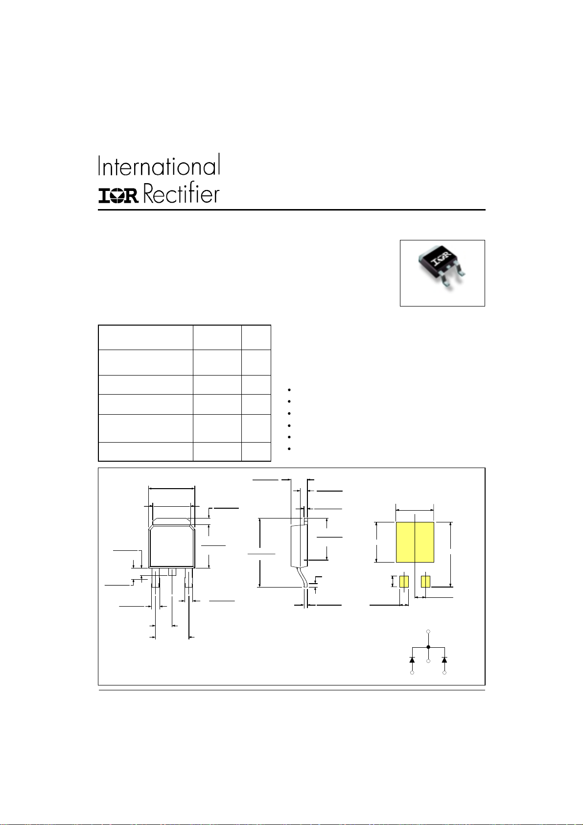
Major Ratings and Characteristics
Characteristics 12CWQ06FN Units
I
Rectangular 12 A
F(AV)
waveform
V
RRM
I
@ tp = 5 µs sine 320 A
FSM
VF@ 6 Apk, TJ = 125°C 0.57 V
(per leg)
TJrange - 55 to 150 °C
6.73 (0.26)
6.35 (0.25)
5.46 (0.21)
5.21 (0.20)
4
1.64 (0.02)
123
1.52 (0.06)
1.15 (0.04)
1.14 (0.04)
2x
0.76 (0.03)
2.28 (0.09)
2x
60 V
1.27 (0.05)
0.88 (0.03)
6.22 (0.24)
5.97 (0.23)
0.89 (0.03)
3x
0.64 (0.02)
4.57 (0.18)
10.42 (0.41)
9.40 (0.37)
2.38 (0.09)
2.19 (0.08)
1 - Anode
2 - Cathode
3 - Anode
4 - Cathode
12 Amp
D-Pak (TO-252AA)
Description/ Features
The 12CWQ06FN surface mount, center tap, Schottky rectifier
series has been designed for applications requiring low forward
drop and small foot prints on PC board. Typical applications are
in disk drives, switching power supplies, converters, freewheeling diodes, battery charging, and reverse battery
protection.
Popular D-PAK outline
Center tap configuration
Small foot print, surface mountable
Low forward voltage drop
High frequency operation
Guard ring for enhanced ruggedness and long term reliability
1.14 (0.04)
0.89 (0.03)
0.58 (0.02)
0.46 (0.02)
6.45 (0.24)
5.68 (0.22)
0.51 (0.02)
MIN.
0.58 (0.02)
0.46 (0.02)
MINIMUM RECOMMENDED FOOTPRINT
5.97 (0.24)
6.48 (0.26)
2x
2.54 (0.10)
1.65 (0.06)
2x
2.28 (0.09)
Base
Common
Cathode
10.67 (0.42)
2x
4
Conform to JEDEC outline D-Pak (Similar to TO-252AA)
Dimensions in millimeters and (inches)
node
Common
Cathode
1
2
3
Anode
www.irf.com 1
12CWQ06FN
Bulletin PD-20547 rev. F 05/02
Voltage Ratings
Part number 12CWQ06FN
VRMax. DC Reverse Voltage (V)
V
Max. Working Peak Reverse Voltage (V)
RWM
60
Absolute Maximum Ratings
Parameters 12CWQ... Units Conditions
I
Max. Average Forward (Per Leg) 6 A 50% duty cycle @ TC = 131°C, rectangular wave form
F(AV)
Current * See Fig. 5 (Per Device) 12
I
Max. Peak One Cycle Non-Repetitive 320 5µs Sine or 3µs Rect. pulse
FSM
Surge Current * See Fig. 7 105 10ms Sine or 6ms Rect. pulse
EASNon-Repet. Avalan. Energy (Per Leg) 7 mJ T
A
= 25 °C, I
J
= 1.2 Amps, L = 10 mH
AS
IARRepetitive Avalanche Current 0.8 A Current decaying linearly to zero in 1 µsec
(Per Leg) Frequency limited by TJ max. VA = 1.5 x VR typical
Following any rated
load condition and with
rated V
RRM
applied
Electrical Specifications
Parameters 12CWQ... Units Conditions
VFMMax. Forward Voltage Drop 0.61 V @ 6A
(Per Leg) * See Fig. 1 (1) 0.79 V @ 12A
0.57 V @ 6A
0.72 V @ 12A
IRMMax. Reverse Leakage Current 3 mA TJ = 25 °C
(Per Leg) * See Fig. 2 (1) 35 mA TJ = 125 °C
V
Threshold Voltage 0.36 V T
F(TO)
= TJ max.
J
rtForward Slope Resistance 24.14 mΩ
CTTyp. Junction Capacitance (Per Leg) 360 pF VR = 5VDC, (test signal range 100Khz to 1Mhz) 25°C
LSTypical Series Inductance (Per Leg) 5.0 nH Measured lead to lead 5mm from package body
(1) Pulse Width < 300µs, Duty Cycle <2%
TJ = 25 °C
TJ = 125 °C
VR = rated V
R
Thermal-Mechanical Specifications
Parameters 12CWQ... Units Conditions
TJMax. Junction Temperature Range (*) - 55 to 150 °C
T
Max. Storage Temperature Range - 55 to 150 °C
stg
R
Max. Thermal Resistance (Per Leg) 3.0 °C/W DC operation * See Fig. 4
thJC
Junction to Case (Per Device) 1.5
wt Approximate Weight 0.3 (0.01) g (oz.)
Case Style D-Pak Similar to TO-252AA
(*) dPtot 1
< thermal runaway condition for a diode on its own heatsink
dTj Rth( j-a)
2
www.irf.com

12CWQ06FN
Bulletin PD-20547 rev. F 05/02
100
F
10
T = 150 C
J
T = 125 C
J
T = 25 C
J
100
T = 150 C
J
125 C
100 C
75 C
50 C
25 C
0 102030405060
Reverse Current - I (mA)
10
R
1
0.1
0.01
0.001
Reverse Voltage - V (V)
Fig. 2 - Typical Values Of Reverse Current
R
Vs. Reverse Voltage (Per Leg)
1000
Instantaneous Forw ard Current - I (A)
T
100
T = 25 C
J
1
0.2 0.4 0.6 0.8 1 1.2 1.4 1.6 1.8 2 2.2 2.4
Fig. 1 - Max. Forward Voltage Drop Characteristics
www.irf.com
Junction C apacitance - C (pF)
10
0 10203040506070
Forward Volta g e Drop - V (V )
FM
Reverse Voltage - V (V)
Fig. 3 - Typical Junction Capacitance
(Per Leg)
Vs. Reverse Voltage (Per Leg)
10
D = 0.75
D = 0.50
D = 0.33
1
thJ C
Therm a l Im ped ance Z ( C/W )
D = 0.25
D = 0.20
0.1
Notes:
Single Pulse
(Thermal Re sistanc e)
0.01
0.00001 0.0001 0.001 0.01 0.1 1
t , Rectang ula r Pulse Du ra tio n (Seconds)
Fig. 4 - Max. Thermal Impedance Z
1
thJC
1. D uty factor D = t / t
2. Pea k T = P x Z + T
Characteristics (Per Leg)
P
DM
t
1
t
2
1
J
DM
thJC
R
2
C
3

12CWQ06FN
Bulletin PD-20547 rev. F 05/02
155
150
145
140
135
130
Square wave (D = 0.50)
80% Rated V applied
125
R
120
115
Allowab le Case Temperature - ( C)
see n ote (2)
110
0123456789
Averag e Fo rward C urrent - I (A)
Fig. 5 - Max. Allowable Case Temperature
Vs. Average Forward Current (Per Leg)
1000
FSM
100
DC
F(AV)
At Any Rated Load Condition
An d W ith Rated V Applied
Follow in g Su rge
RRM
6
D = 0.20
5
D = 0.25
D = 0.33
D = 0.50
4
3
D = 0.75
RMS Limit
2
Average Power Loss - (Watts)
1
0
0123456789
Average Forward Current - I (A)
Fig. 6 - Forward Power Loss Characteristics
(Per Leg)
DC
F(AV)
(2) Formula used: TC = TJ - (Pd + Pd
Pd = Forward Power Loss = I
Pd
= Inverse Power Loss = VR1 x IR (1 - D); IR @ V
REV
4
Non-Repetitive Surge Current - I (A)
10
10 100 1000 10000
Square W ave Pulse Dura tion - t (microsec)
p
Fig. 7 - Max. Non-Repetitive Surge Current (Per Leg)
) x R
thJC
;
F(AV)
/ D) (see Fig. 6);
= 80% rated V
R1
R
F(AV)
REV
x VFM @ (I
www.irf.com

Marking Information
EXAMPLE: THIS IS AN 12CWQ06FN
Tape & Reel Information
TR
FEED DIRECTION
4.1 (0.16)
3.9 (0.15)
2.1 (0.83)
1.9 (0.07)
12.1 (0.48)
11.9 (0.47)
INTERNATIONAL
RECTIFIER LOGO
ASSEMBLY
LOT CODE
1.85 (0.07)
1.65 (0.06)
1.85 (0.07)
1.65 (0.06)
DIA.
2.6 (0.10)
1.5 (0.06)
7.6 (0.30)
7.4 (0.29)
DIA.
4 (K)
12CWQ06FN
712A
5K3A
2 (K)
1 (A) 3 (A)
0.35 (0.01)
0.25 (0.01)
7.0 (0.28)
6.8 (0.26)
2.75 (0.11)
2.55 (0.10)
12CWQ06FN
Bulletin PD-20547 rev. F 05/02
PART NUMBER
DATE CODE (YWWA)
Y = YEAR
WW = WEEK
A = LINE
16.3 (0.64)
15.7 (0.62)
375 (14.17)
DIA. MAX.
TRR
FEED DIRECTION
TRL
FEED DIRECTION
13 (0.52) DIA.
4.1 (0.16)
3.9 (0.15)
2.1 (0.83)
1.9 (0.07)
8.1 (0.32)
7.9 (0.31)
4.1 (0.16)
3.9 (0.15)
2.1 (0.83)
1.9 (0.07)
8.1 (0.32)
7.9 (0.31)
1.85 (0.07)
1.65 (0.06)
1.85 (0.07)
1.65 (0.06)
7.6 (0.30)
7.4 (0.29)
2.6 (0.10)
1.5 (0.06)
1.85 (0.07)
1.65 (0.06)
1.85 (0.07)
1.65 (0.06)
7.6 (0.30)
7.4 (0.29)
2.6 (0.10)
1.5 (0.06)
22.4 (0.88)
50 (1.97) DIA.
DIA.
DIA.
0.35 (0.01)
0.25 (0.01)
10.6 (0.42)
10.4 (0.41)
DIA.
DIA.
2.75 (0.11)
2.55 (0.10)
0.35 (0.01)
0.25 (0.01)
10.6 (0.42)
10.4 (0.41)
2.75 (0.11)
2.55 (0.10)
TO-252AA Tape & Reel
When ordering, indicate the part
number, part orientation, and the
quantity. Quantities are in multiples
of 2,000 pieces per reel for TR and
multiples of 3,000 pieces per reel
for both TRL and TRR.
16.3 (0.64)
15.7 (0.62)
16.3 (0.64)
15.7 (0.62)
www.irf.com
5

12CWQ06FN
Bulletin PD-20547 rev. F 05/02
12CWQ06FN
********************************************
* This model has been developed by *
* Wizard SPICE MODEL GENERATOR (1999) *
* International Rectifier Corporation) *
* contains Proprietary Information *
********************************************
* SPICE Model Diode is composed by a *
* simple diode plus paralled VCG2T *
********************************************
.SUBCKT 12CWQ06FN ANO CAT
D1 ANO 1 DMOD (0.03191)
*Define diode model
.MODEL DMOD D(IS=8.95944674613071E-05A,N=1.03666612245428,BV=67V,
+ IBV=0.232083097618696A,RS= 0.00089348,CJO=2.04854724822182E-08,
+ VJ=1.34189135485872,XTI=2, EG=0.732501148466477)
********************************************
*Implementation of VCG2T
VX 1 2 DC 0V
R1 2 CAT TRES 1E-6
.MODEL TRES RES(R=1,TC1=52.5561105683715)
GP1 ANO CAT VALUE={-ABS(I(VX))*(EXP((((-3.507402E-03/52.55611)*((V(2,CAT)*1E6)/
(I(VX)+1E-6)-1))+1)*4.963732E-02*ABS(V(ANO,CAT)))-1)}
********************************************
.ENDS 12CWQ06FN
Thermal Model Subcircuit
.SUBCKT 12CWQ06FN 5 1
CTHERM1 5 4 8.75E-04
CTHERM2 4 3 5.33E+01
CTHERM3 3 2 2.05E+02
CTHERM4 2 1 7.61E+02
RTHERM1 5 4 1.00E-07
RTHERM2 4 3 1.65E+00
RTHERM1 3 2 1.12E+00
RTHERM1 2 1 2.29E-01
.ENDS 12CWQ06FN
This product has been designed and qualified for Industrial Level.
IR WORLD HEADQUARTERS: 233 Kansas St., El Segundo, California 90245, USA Tel: (310) 252-7105
6
Data and specifications subject to change without notice.
Qualification Standards can be found on IR's Web site.
TAC Fax: (310) 252-7309
Visit us at www.irf.com for sales contact information. 05/02
www.irf.com
 Loading...