

D-PAK
PRODUCT SUMMARY
I
F(AV)
V
R
Schottky Rectifier,
Base
common
cathode
4
2
Common
cathode
13
Anode Anode
2 x 6 A
30 V
12CWQ03FNPbF
Vishay High Power Products
2 x 6 A
FEATURES
• Popular D-PAK outline
• Center tap configuration
• Small foot print, surface mountable
• Low forward voltage drop
• High frequency operation
• Guard ring for enhanced ruggedness and long term
reliability
• Compliant to RoHS directive 2002/95/EC
• AEC-Q101 qualified
DESCRIPTION
The 12CWQ03FNPbF surface mount, center tap, Schottky
rectifier series has been designed for applications requiring
low forward drop and small foot prints on PC board. Typical
applications are in disk drives, switching power supplies,
converters, freewheeling diodes, battery charging, and
reverse battery protection.
MAJOR RATINGS AND CHARACTERISTICS
SYMBOL CHARACTERISTICS VALUES UNITS
I
F(AV)
V
RRM
I
FSM
V
F
T
J
Rectangular waveform 12 A
30 V
tp = 5 µs sine 320 A
6 Apk, TJ = 125 °C (per leg) 0.37 V
Range - 55 to 150 °C
VOLTAGE RATINGS
PARAMETER SYMBOL 12CWQ03FNPbF UNITS
Maximum DC reverse voltage V
Maximum working peak reverse voltage V
R
RWM
30 V
ABSOLUTE MAXIMUM RATINGS
PARAMETER SYMBOL TEST CONDITIONS VALUES UNITS
Maximum average
forward current
See fig. 5
Maximum peak one cycle
non-repetitive surge current per leg
See fig. 7
Non-repetitive avalanche energy per leg E
Repetitive avalanche current per leg I
per leg
I
per device 12
F(AV)
I
FSM
AS
AR
50 % duty cycle at TC = 135 °C, rectangular waveform
5 µs sine or 3 µs rect. pulse
10 ms sine or 6 ms rect. pulse 130
TJ = 25 °C, IAS = 2.0 A, L = 5 mH 10 mJ
Current decaying linearly to zero in 1 µs
Frequency limited by T
maximum VA = 1.5 x VR typical
J
Following any rated
load condition and with
rated V
RRM
applied
6
A
320
A
2.0 A
Document Number: 94132 For technical questions, contact: diodestech@vishay.com
Revision: 08-Jul-09 1
www.vishay.com
12CWQ03FNPbF
Vishay High Power Products
Schottky Rectifier,
2 x 6 A
ELECTRICAL SPECIFICATIONS
PARAMETER SYMBOL TEST CONDITIONS VALUES UNITS
Maximum forward
voltage drop per leg
V
See fig. 1
Maximum reverse
leakage current per leg
I
RM
See fig. 2
Threshold voltage V
Forward slope resistance r
Typical junction capacitance per leg C
Typical series inductance per leg L
FM
F(TO)
S
6 A
12 A 0.55
(1)
6 A
12 A 0.49
TJ = 25 °C
(1)
= 125 °C 58
T
J
TJ = TJ maximum
t
T
VR = 5 VDC (test signal range 100 kHz to 1 MHz), 25 °C 590 pF
Measured lead to lead 5 mm from package body 5.0 nH
T
= 25 °C
J
= 125 °C
T
J
= Rated V
V
R
R
Note
(1)
Pulse width < 300 µs, duty cycle < 2 %
THERMAL - MECHANICAL SPECIFICATIONS
PARAMETER SYMBOL TEST CONDITIONS VALUES UNITS
Maximum junction and storage
temperature range
Maximum thermal resistance,
junction to case
per leg
per device 1.5
Approximate weight
Marking device Case style D-PAK (similar to TO-252AA) 12CWQ03FN
Note
dP
(1)
------------dT
1
tot
J
thermal runaway condition for a diode on its own heatsink
--------------<
R
thJA
(1)
T
, T
J
Stg
R
thJC
DC operation
See fig. 4
0.47
0.37
3
0.196 V
21.66 mΩ
- 55 to 150 °C
3.0
0.3 g
0.01 oz.
V
mA
°C/W
www.vishay.com For technical questions, contact: diodestech@vishay.com
Document Number: 94132
2 Revision: 08-Jul-09
12CWQ03FNPbF
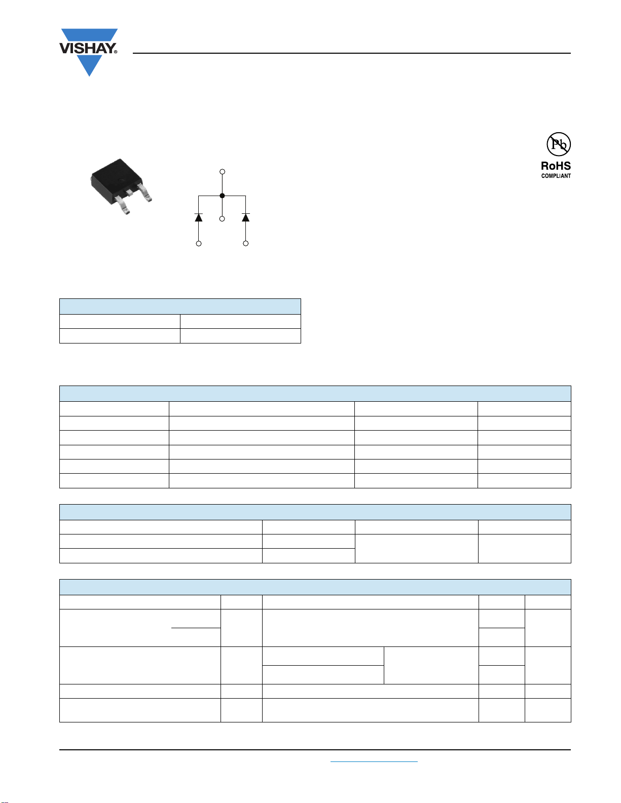
100
10
Current (A)
- Instantaneous Forward
F
I
1
01.8
0.2
0.4 0.8 1.2
V
- Forward Voltage Drop (V)
FM
TJ = 150 °C
T
= 125 °C
J
= 25 °C
T
J
1.6
1.41.00.6
Fig. 1 - Maximum Forward Voltage Drop Characteristics
(Per Leg)
1000
Schottky Rectifier,
2 x 6 A
- Reverse Current (mA)
R
I
Vishay High Power Products
1000
100
10
TJ = 100 °C
1
0.1
0.01
0.001
TJ = 25 °C
0102030
TJ = 75 °C
TJ = 50 °C
5
V
- Reverse Voltage (V)
R
Fig. 2 - Typical Values of Reverse Current vs.
Reverse Voltage (Per Leg)
TJ = 150 °C
TJ = 125 °C
2515
TJ = 25 °C
- Junction Capacitance (pF)
T
C
100
51525
0203035
10
V
- Reverse Voltage (V)
R
Fig. 3 - Typical Junction Capacitance vs. Reverse Voltage (Per Leg)
10
1
P
D = 0.75
D = 0.50
D = 0.33
D = 0.25
0.1
D = 0.20
- Thermal Impedance (°C/W)
thJC
Z
0.01
0.00001 0.0001 0.001 0.01 0.1 1
Single pulse
(thermal resistance)
Notes:
1. Duty factor D = t
2. Peak TJ = PDM x Z
DM
t
1
1/t2
thJC
t1 - Rectangular Pulse Duration (s)
Fig. 4 - Maximum Thermal Impedance Z
Characteristics (Per Leg)
thJC
t
2
+ T
C
Document Number: 94132 For technical questions, contact: diodestech@vishay.com
www.vishay.com
Revision: 08-Jul-09 3
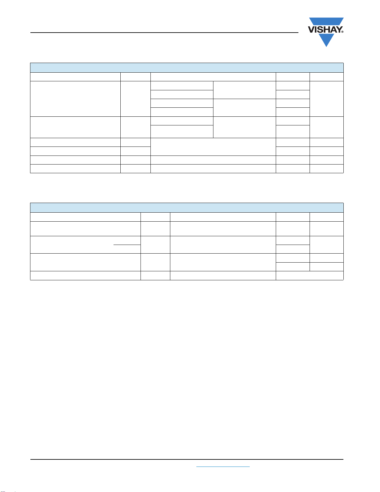
12CWQ03FNPbF
Vishay High Power Products
150
145
140
135
130
125
Allowable Case Temperature (°C)
120
Square wave (D = 0.50)
80 % rated V
See note (1)
0 8 94
1357
I
F(AV)
applied
R
26
- Average Forward Current (A)
Fig. 5 - Maximum Allowable Case Temperature vs.
Average Forward Current (Per Leg)
1000
Schottky Rectifier,
2 x 6 A
DC
4.0
3.5
3.0
2.5
2.0
1.5
1.0
Average Power Loss (W)
0.5
0
0
Fig. 6 - Forward Power Loss Characteristics (Per Leg)
At any rated load condition
and with rated V applied
following surge
RRM
D = 0.20
D = 0.25
D = 0.33
D = 0.50
D = 0.75
DC
1
2
I
- Average Forward Current (A)
F(AV)
46 9
35
RMS limit
7
8
- Non-Repetitive Surge Current (A)
100
FSM
I
10
100
1000
10 000
tp - Square Wave Pulse Duration (µs)
Fig. 7 - Maximum Non-Repetitive Surge Current (Per Leg)
Note
(1)
Formula used: TC = TJ - (Pd + Pd
Pd = Forward power loss = I
Pd
= Inverse power loss = VR1 x IR (1 - D); IR at VR1 = 80 % rated V
REV
F(AV)
) x R
REV
x VFM at (I
thJC
;
F(AV)
/D) (see fig. 6);
R
www.vishay.com For technical questions, contact: diodestech@vishay.com
Document Number: 94132
4 Revision: 08-Jul-09
12CWQ03FNPbF
ORDERING INFORMATION TABLE
Device code
12 C W Q 03 FN TRL PbF
1 - Current rating (12 A)
2 - Center tap configuration
- Package identifier:
3
4
4 - Schottky “Q” series
- Voltage rating (03 = 30 V)
5
- FN = TO-252AA
6
-
7
- PbF = Lead (Pb)-free
8
Schottky Rectifier,
2 x 6 A
51324678
-
W = D-PAK
None = Tube (50 pieces)
TR = Tape and reel
TRL = Tape and reel (left oriented)
TRR = Tape and reel (right oriented)
Vishay High Power Products
LINKS TO RELATED DOCUMENTS
Dimensions www.vishay.com/doc?95016
Part marking information www.vishay.com/doc?95059
Packaging information www.vishay.com/doc?95033
Document Number: 94132 For technical questions, contact: diodestech@vishay.com
Revision: 08-Jul-09 5
www.vishay.com

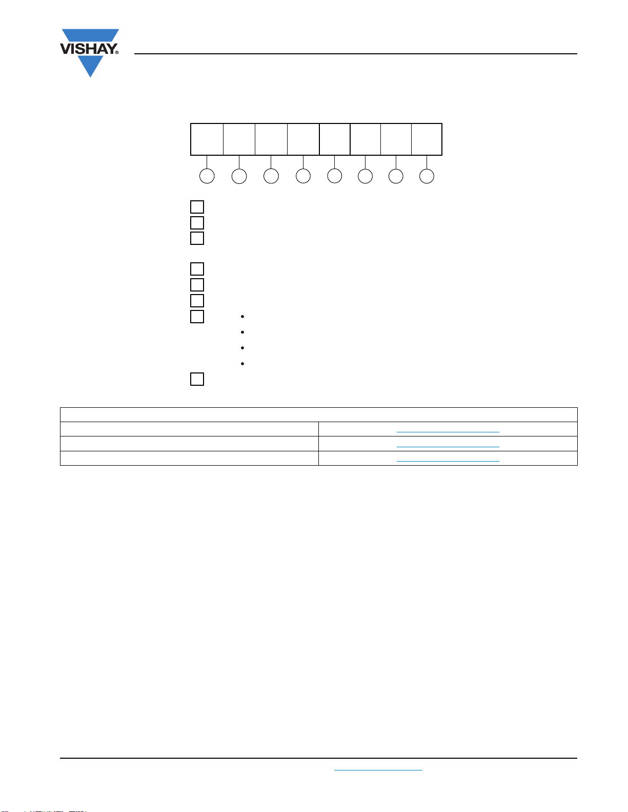
D-PAK (TO-252AA)
Part Marking Information
Vishay High Power Products
Assembly
lot code
xxxxxxx
V P012C
YYYY
Part number
Product version (optional):
P = Lead (Pb)-free
None = Standard
Date code:
Year 0 = 2000
Week 12
Line C
Example: This is a xxxxxxx with
assembly lot code YYYY,
assembled on WW 12, 2000
in the assembly line “C”
Document Number: 95059 For technical questions concerning discrete products, contact: diodes-tech@vishay.com
Revision: 30-Oct-08 For technical questions concerning module products, contact: ind-modules@vishay.com
www.vishay.com
1
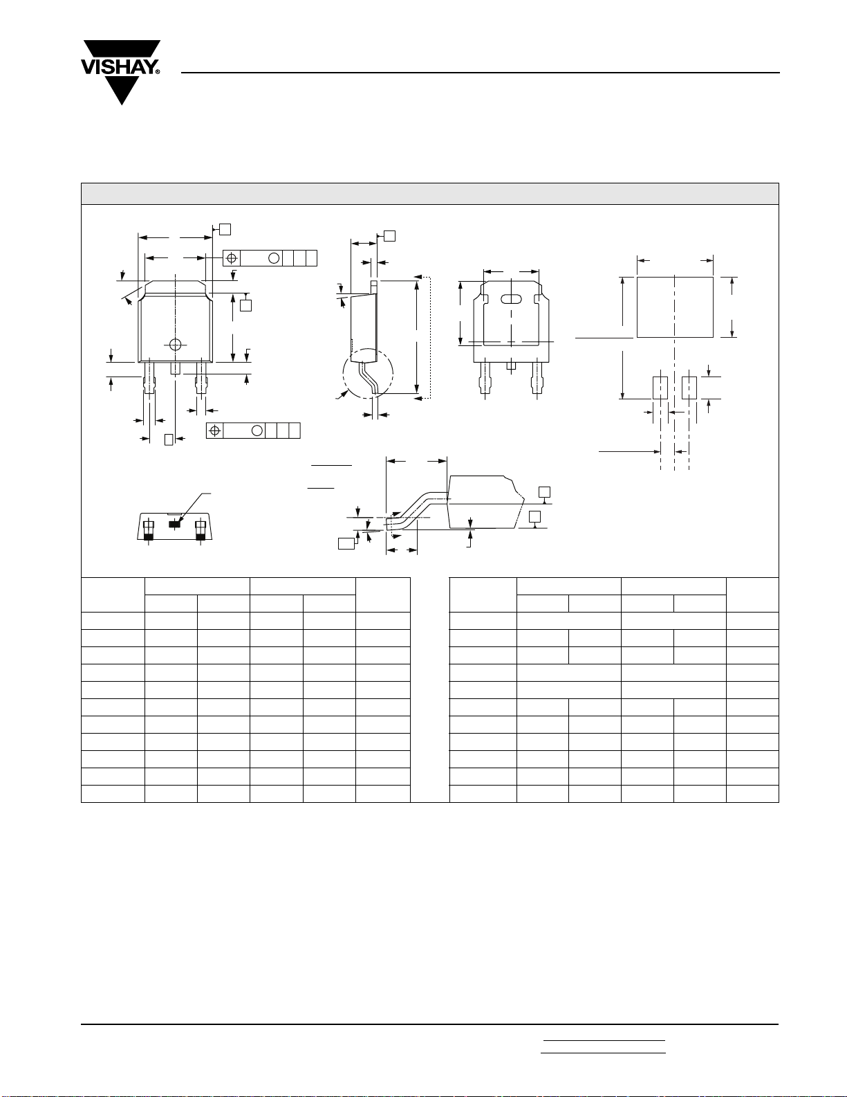
D-PAK (TO-252AA)
DIMENSIONS in millimeters and inches
Outline Dimensions
Vishay High Power Products
Ø 2
(2) L5
b2
SYMBOL
(5)
(3)
3
A
L3 (3)
D (5)
b
0.010
Lead tip
0.010
B
L4
M
M
CAB
Detail “C”
CAB
Rotated 90 °CW
Ø 1
Detail “C”
Scale: 20:1
Gauge
plane
L2
E
b3
4
1
2
e
2 x
MILLIMETERS INCHES
MIN. MAX. MIN. MAX. MIN. MAX. MIN. MAX.
C
A
c2
A
Seating
plane
Ø
c
(L1)
C
C
L
D1
H
3241
A
A1
NOTES SYMBOL
E1
0.488 (12.40)
0.409 (10.40)
0.06
(1.524)
0.093 (2.38)
0.085 (2.18)
H
(7)
C
Seating
plane
MILLIMETERS INCHES
MIN.
Pad layout
0.265
MIN.
(6.74)
0.245
(6.23)
0.089
(2.28)
NOTES
A 2.18 2.39 0.086 0.094 e 2.29 BSC 0.090 BSC
A1 - 0.13 - 0.005 H 9.40 10.41 0.370 0.410
b 0.64 0.89 0.025 0.035 L 1.40 1.78 0.055 0.070
b2 0.76 1.14 0.030 0.045 L1 2.74 BSC 0.108 REF.
b3 4.95 5.46 0.195 0.215 3 L2 0.51 BSC 0.020 BSC
c 0.46 0.61 0.018 0.024 L3 0.89 1.27 0.035 0.050 3
c2 0.46 0.89 0.018 0.035 L4 - 1.02 - 0.040
D 5.97 6.22 0.235 0.245 5 L5 1.14 1.52 0.045 0.060 2
D1 5.21 - 0.205 - 3 Ø 0° 10° 0° 10°
E 6.35 6.73 0.250 0.265 5 Ø1 0° 15° 0° 15°
E1 4.32 - 0.170 - 3 Ø2 25° 35° 25° 35°
Notes
(1)
Dimensioning and tolerancing as per ASME Y14.5M-1994
(2)
Lead dimension uncontrolled in L5
(3)
Dimension D1, E1, L3 and b3 establish a minimum mounting surface for thermal pad
(4)
Section C - C dimension apply to the flat section of the lead between 0.13 and 0.25 mm (0.005 and 0.10") from the lead tip
(5)
Dimension D, and E do not include mold flash. Mold flash shall not exceed 0.127 mm (0.005") per side. These dimensions are measured at
the outermost extremes of the plastic body
(6)
Dimension b1 and c1 applied to base metal only
(7)
Datum A and B to be determined at datum plane H
(8)
Outline conforms to JEDEC outline TO-252AA
MIN.
MIN.
Document Number: 95016 For technical questions concerning discrete products, contact: diodes-tech@vishay.com
Revision: 04-Nov-08 For technical questions concerning module products, contact: ind-modules@vishay.com
www.vishay.com
1

D-PAK
TAPE AND REEL INFORMATION in millimeters (inches)
1.6 (0.06)
1.5 (0.05)
1.85 (0.07)
1.65 (0.06)
TR
4.1 (0.16)
3.9 (0.15)
2.1 (0.83)
1.9 (0.07)
DIA.
7.6 (0.30)
7.4 (0.29)
Packaging Information
Vishay High Power Products
0.35 (0.01)
0.25 (0.01)
7.0 (0.28)
6.8 (0.26)
16.3 (0.64)
15.7 (0.62)
Feed direction
TRR
Feed direction
TRL
Feed direction
12.1 (0.48)
11.9 (0.47)
4.1 (0.16)
3.9 (0.15)
2.1 (0.83)
1.9 (0.07)
8.1 (0.32)
7.9 (0.31)
4.1 (0.16)
3.9 (0.15)
2.1 (0.83)
1.9 (0.07)
8.1 (0.32)
7.9 (0.31)
2.6 (0.10)
1.5 (0.06)
1.6 (0.06)
1.5 (0.05)
1.85 (0.07)
1.65 (0.06)
7.6 (0.30)
7.4 (0.29)
1.6 (0.06)
1.5 (0.05)
1.85 (0.07)
1.65 (0.06)
7.6 (0.30)
7.4 (0.29)
DIA.
2.6 (0.10)
1.5 (0.06)
DIA.
2.6 (0.10)
1.5 (0.06)
DIA.
DIA.
DIA.
2.75 (0.11)
2.55 (0.10)
0.35 (0.01)
0.25 (0.01)
10.6 (0.42)
10.4 (0.41)
2.75 (0.11)
2.55 (0.10)
0.35 (0.01)
0.25 (0.01)
10.6 (0.42)
10.4 (0.41)
2.75 (0.11)
2.55 (0.10)
16.3 (0.64)
15.7 (0.62)
16.3 (0.64)
15.7 (0.62)
13 (0.52) DIA.
375 (14.17)
DIA. MAX.
22.4 (0.88)
50 (1.97) DIA.
D-PAK tape and reel
When ordering, indicate the part
number, part orientation, and the
quantity. Quantities are in multiples
of 2000 pieces per reel for TR and
multiples of 3000 pieces per reel
for both TRL and TRR.
Document Number: 95033 For technical questions concerning discrete products, contact: diodestech@vishay.com
Revision: 16-Sep-09 For technical questions concerning module products, contact: indmodules@vishay.com
www.vishay.com
1

Legal Disclaimer Notice
Vishay
Disclaimer
All product specifications and data are subject to change without notice.
Vishay Intertechnology, Inc., its affiliates, agents, and employees, and all persons acting on its or their behalf
(collectively, “Vishay”), disclaim any and all liability for any errors, inaccuracies or incompleteness contained herein
or in any other disclosure relating to any product.
Vishay disclaims any and all liability arising out of the use or application of any product described herein or of any
information provided herein to the maximum extent permitted by law. The product specifications do not expand or
otherwise modify Vishay’s terms and conditions of purchase, including but not limited to the warranty expressed
therein, which apply to these products.
No license, express or implied, by estoppel or otherwise, to any intellectual property rights is granted by this
document or by any conduct of Vishay.
The products shown herein are not designed for use in medical, life-saving, or life-sustaining applications unless
otherwise expressly indicated. Customers using or selling Vishay products not expressly indicated for use in such
applications do so entirely at their own risk and agree to fully indemnify Vishay for any damages arising or resulting
from such use or sale. Please contact authorized Vishay personnel to obtain written terms and conditions regarding
products designed for such applications.
Product names and markings noted herein may be trademarks of their respective owners.
Document Number: 91000 www.vishay.com
Revision: 18-Jul-08 1
 Loading...