

Page 1
Preliminary Data Sheet I2145 12/97
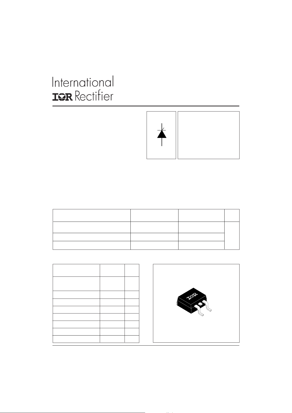
SAFE
IR
Series
10TTS08S
SURFACE MOUNTABLE
PHASE CONTROL SCR
Description/Features
The 10TTS08S SAFEIR series of silicon
controlled rectifiers are specifically designed for
medium power switching and phase control
applications. The glass passivation technology
used has reliable operation up to 125° C junction
temperature.
Typical applications are in input rectification (soft
start) and these products are designed to be used
with International Rectifier input diodes, switches
and output rectifiers which are available in identical package outlines.
Output Current in Typical Applications
Applications Single-phase Bridge Three-phase Bridge Units
NEMA FR-4 or G10 glass fabric-based epoxy
with 4 oz (140µm) copper
Aluminum IMS, R
Aluminum IMS with heatsink, R
TA = 55°C, TJ = 125°C, footprint 300mm
Major Ratings and Characteristics
= 15°C/W 6.3 9.5 A
thCA
= 5°C/W 14.0 18.5
thCA
2
2.5 3.5
Package Outline
V
I
TSM
V
< 1.15V @ 6.5A
T
= 140A
= 800V
RRM
Characteristics 10TTS08S Units
I
Sinusoidal 6.5 A
T(AV)
waveform
I
RMS
V
V
/
RRM
DRM
I
TSM
V
@ 6.5 A, TJ = 25°C 1.15 V
T
dv/dt 150 V/µs
di/dt 100 A/µs
T
range - 40 to 125 °C
J
10 A
800 V
140 A
D2 PAK (SMD-220)
1
Page 2
10TTS08S SAFE
IR
Series
Preliminary Data Sheet I2145 12/97
Voltage Ratings
V
, maximum V
RRM
, maximum I
DRM
Part Number peak reverse voltage peak direct voltage 1 25°C
VVmA
10TTS08S 800 800 1.0
Absolute Maximum Ratings
Parameters 10TTS08S Units Conditions
I
Max. Average On-state Current 6.5 A @ TC = 112° C, 180° conduction half sine wave
T(AV)
I
Max. RMS On-state Current 10
T(RMS)
I
Max. Peak One Cycle Non-Repetitive 120 A 10ms Sine pulse, rated V
TSM
Surge Current 140 10ms Sine pulse, no voltage reapplied, TJ = 125°C
I2t Max. I2t for fusing 72 A2s 10ms Sine pulse, rated V
100 10ms Sine pulse, no voltage reapplied, TJ = 125°C
I2√t Max. I2√t for fusing 1000 A2√s t = 0.1 to 10ms, no voltage reapplied, TJ = 125°C
VTMMax. On-state Voltage Drop 1.15 V @ 6.5A, TJ = 25°C
r
On-state slope resistance 17.3 mΩ TJ = 125°C
t
V
Threshold Voltage 0.85 V
T(TO)
IRM/IDMMax.Reverse and Direct 0.05 mA TJ = 25 °C
Leakage Current 1.0 TJ = 125 °C
I
Typ. Holding Current 30 mA Anode Supply = 6V, Resistive load, Initial IT=1A
H
I
Max. Latching Current 50 mA Anode Supply = 6V, Resistive load
L
dv/dt Max. rate of rise of off-state Voltage 15 0 V/µs T
= 25°C
J
di/dt Max. rate of rise of turned-on Current 100 A/µs
applied, TJ = 125°C
RRM
applied, TJ = 125°C
RRM
VR = rated V
RRM
/ V
RRM/IDRM
DRM
2
Page 3
10TTS08S SAFE
IR
Preliminary Data Sheet I2145 12/97
Triggering
Parameters 10TTS08S Units Conditions
PGMMax. peak Gate Power 8.0 W
P
Max. average Gate Power 2.0
G(AV)
Max. paek positive Gate Current 1.5 A
+ I
GM
- V
Max. paek negative Gate Voltage 10 V
GM
IGTMax. required DC Gate Current 2 0 mA Anode supply = 6V, resistive load, TJ = - 65°C
to trigger 15 Anode supply = 6V, resistive load, TJ = 25°C
10 Anode supply = 6V, resistive load, T
V
Max. required DC Gate Voltage 1.2 V Anode supply = 6V, resistive load, TJ = - 65°C
GT
to trigger 1 Anode supply = 6V, resistive load, T
0.7 Anode supply = 6V, resistive load, TJ = 125°C
V
Max. DC Gate Voltage not to trigger 0.2 TJ = 125°C, V
GD
IGDMax. DC Gate Current not to trigger 0.1 mA TJ = 125°C, V
= rated value
DRM
= rated value
DRM
= 125°C
J
= 25°C
J
Switching
Series
Parameters 10TTS08S Units Conditions
t
Typical turn-on time 0.8 µs TJ = 25°C
gt
t
Typical reverse recovery time 3 TJ = 125°C
rr
t
Typical turn-off time 100
q
Thermal-Mechanical Specifications
Parameters 10TTS08S Units Conditions
TJMax. Junction Temperature Range - 40 to 125 °C
Max. Storage Temperature Range - 40 to 125 °C
T
stg
Soldering Temperature 240 °C for 10 seconds (1.6mm from case)
R
Max. Thermal Resistance Junction 1.5 °C/W DC operation
thJC
to Case
R
Typ. Thermal Resistance Junction 40 °C/W
thJA
to Ambient (PCB Mount)**
wt Approximate Weight 2 (0.07) g (oz.)
T Case Style D
**When mounted on 1" square (650mm2) PCB of FR-4 or G-10 material 4 oz (140µm) copper 40°C/W
For recommended footprint and soldering techniques refer to application note #AN-994
2
Pak (SMD-220)
3
Page 4

10TTS08S SAFE
IR
Preliminary Data Sheet I2145 12/97
Series
125
120
115
110
105
Maximum Allo w a ble Case Te mperature (°C)
01234567
Average On-state Current (A)
10TTS08
R (DC) = 1.5 K/W
thJC
Cond uction Angle
30°
60°
90°
120°
Fig. 1 - Current Rating Characteristics
8
7
6
5
4
3
2
1
0
Max im u m Av erage On- sta t e P ower Lo s s ( W)
01234567
180°
120°
90°
60°
30°
RMS Limit
Conduction Angle
10TTS08
T = 125°C
J
Average On-state Current (A)
180°
125
120
115
110
105
Max im u m Allowabl e Ca se Temperature (°C)
024681012
10TTS08
R (DC) = 1.5 K/W
thJC
Conduction Period
30°
60°
90°
120°
180°
DC
Average On-state Current (A)
Fig. 2 - Current Rating Characteristics
12
DC
180°
10
120°
90°
60°
8
30°
6
RMS Limit
4
2
0
Maximum Average On-state Power Loss (W)
024681012
Average On-state Current (A)
Conduction Period
10TTS08
T = 125°C
J
Fig. 3 - On-state Power Loss Characteristics Fig. 4 - On-state Power Loss Characteristics
130
At Any Rated Load Condition And With
Rated V Applied Following Surge.
10TTS08
RRM
Initi a l T = 125°C
J
@ 60 Hz 0.0083 s
@ 50 Hz 0.0100 s
120
110
100
90
80
70
Peak Half Sine Wave On-state Current (A)
60
110100
Number Of Equal Amplitude Half Cycle Current Pulses (N)
150
Maxim u m Non Repetiti ve Surge Curre nt
140
130
120
110
100
90
80
70
60
Peak Half Sine Wave On-state Current (A)
50
Ve rsu s Pu ls e T r a in Durat ion. C ontr o l
Of Conduct ion May Not Be Maint ained.
10TTS08
0.01 0.1 1
Pulse Train Duration (s)
Initial T = 1 25°C
No Voltage Reapplied
Rated V Reapplied
RRM
Fig. 6 - Maximum Non-Repetitive Surge Current Fig. 7 - Maximum Non-Repetitive Surge Current
4
J
Page 5

10TTS08S SAFE
IR
Series
Preliminary Data Sheet I2145 12/97
1000
10TTS08
100
T = 25°C
10
Instantaneous On -state Current (A)
1
0.511.522.533.5
Instantaneous On-state Voltage (V)
J
T = 125°C
J
Fig. 7 - On-state Voltage Drop Characteristics
10
Steady State Value
thJC
1
D = 0.50
D = 0.33
D = 0.25
D = 0.17
D = 0.08
0.1
Single Pulse
(DC Operati on)
10TTS08
Transien t Thermal Impedance Z (°C/W)
0.01
0.0001 0.001 0.01 0.1 1
Square Wave Pulse Duration (s)
Fig. 8 - Thermal Impedance Z
Characteristics
thJC
5
Page 6

10TTS08S SAFE
IR
Preliminary Data Sheet I2145 12/97
Marking Information
EXAMPLE: THIS IS AN 10TTS08S
Tape & Reel Information
TRR
F E E D DIRECTION
TRL
1.85 (0.073)
1.65 (0.065)
Series
4.10 (0.161)
3.90 (0.153)
10.90 (0.429)
10.70 (0.421)
INTERNATIONAL
RECTIFIER LOGO
ASSEMBLY
LOT CODE
1.60 (0.063)
1.50 (0.059)
16.10 (0.634)
15.90 (0.626)
9G3A
1.60 (0.063)
1.50 (0.059)
11.60 (0.457)
11.40 (0.449)
1.75 (0.069)
1.25 (0.049)
(A)
10TTS08S
9512
(K) (G)
DIA.
15.42 (0.609)
15.22 (0.601)
DIA.
PART NUMBER
DATE CODE (YYWW)
YY = YEAR
WW = WEEK
0.368 (0.0145)
0.342 (0.0135)
24.30 (0.957)
23.90 (0.941)
4.72 (0.186)
4.52 (0.178)
FEED DI RECTI ON
360 (14.173)
DIA. MAX.
6
13.50 (0.532)
12.80 (0.504)
DIA.
Dimensions in millimeters and inches
26.40 (1.039)
24.40 (0.961)
60 (2.3 62)
DIA. MIN.
SMD-220 Tape & Reel
When ordering, indicate the part
number, part orientation, and the
quantity. Quantities are in multiples
of 800 pieces per reel for both
TRL and TRR.
Page 7

Outline Table
1.40 (0.055)
3X
1.14 (0.045)
93°
15.49 (0.61)
14.73 (0.58)
1 (K) Cathode
2 (A) Anode
3 (G) Gate
Dimensions in millimeters and inches
10.16 (0.40)
REF.
(K) (G)
13
2
(A)
2.61 (0.10)
2.32 (0.09)
8.89 (0.35)
REF.
0.93 (0.37)
2X
0.69 (0.27)
5.08 (0 .20) REF.
6.47 (0.25)
6.18 (0.24)
4.57 (0.18)
4.32 (0.17)
0.61 (0.02) M AX.
10TTS08S SAFE
IR
Preliminary Data Sheet I2145 12/97
4.69 (0.18)
4.20 (0.16)
1.32 (0.05)
1.22 (0.05)
5.28 (0.21)
4.78 (0.19)
0.55 (0.02)
0.46 (0.02)
MINIMUM RECOMMENDED FOOTPRINT
11.43 (0.45)
8.89 (0.35)
17.78 (0.70)
3.81 (0.15)
2.08 (0.08)
2X
2.54 (0.10)
2X
Series
Ordering Information Table
Device Code
10 T T S 08 S TRL
1
1 - Current Rating, RMS value
2 - Circuit Configuration
T = Single Thyristor
3 - Package
T = TO-220AC
4 - Type of Silicon
S = Converter Grade
5 - Voltage code: Code x 100 = V
6 - S = TO-220 D2Pak (SMD 220) Version
7 - Tape and Reel Option
TRL = Left Reel
TRR = Right Orientation Reel
3
RRM
524
2
(A)
6
7
1 (K)
(G) 3
7
Page 8

10TTS08S SAFE
Preliminary Data Sheet I2145 12/97
IR
Series
WORLD HEADQUARTERS: 233 Kansas St., El Segundo, California 90245 U.S.A Tel: (310) 322-3331 Fax: (310) 322-3332
EUROPEAN HEADQUARTERS: Hurst Green, Oxted, Surrey RH8 9BB, U.K. Tel: ++ 44 1883 732020 Fax: ++ 44 1883 733408
http://www.irf.com Fax-On-Demand: +44 1883 733420 Data and specifications subject to change without notice 12/97
IR CANADA: 7231 Victoria Park Ave., Suite #201, Markham, Ontario L3R 2Z8 Tel: (905) 475 1897. Fax: (905) 475 8801
IR GERMANY: Saalburgstrasse 157, 61350 Bad Homburg Tel: ++ 49 6172 96590 Fax: ++ 49 6172 965933
IR ITALY: Via Liguria 49, 10071 Borgaro, Torino Tel: ++ 39 11 4510111 Fax: ++ 39 11 4510220
IR FAR EAST: K&H Bldg., 2F, 30-4 Nishi-Ikebukuro 3-Chome, Toshima-Ku, Tokyo, Japan 171 Tel: 81 3 3983 0086 Fax: 81 3 3983 0642
IR SOUTHEAST ASIA: 315 Outram Road, # 10-02 Tan Boon Liat Building, SINGAPORE 0316. Tel: 65 221 8371. Fax: 65 221 8372.
8
 Loading...