

Bulletin PD-20519 rev. L 07/04
10MQ060N
SCHOTTKY RECTIFIER
Major Ratings and Characteristics
Characteristics Value Units
I FDC 2.1 A
V
RRM
I
@ tp = 5 µs sine 40 A
FSM
VF@ 1.5Apk, TJ=125°C 0.63 V
TJrange - 55 to 150 °C
60 V
2.1 Amp
I
= 2.1Amp
F(AV)
VR = 60V
Description/ Features
The 10MQ060N surface mount Schottky rectifier has been
designed for applications requiring low forward drop and very
small foot prints on PC boards. Typical applications are in disk
drives, switching power supplies, converters, free-wheeling
diodes, battery charging, and reverse battery protection.
Small foot print, surface mountable
Low forward voltage drop
High frequency operation
Guard ring for enhanced ruggedness and long term
reliability
www.irf.com
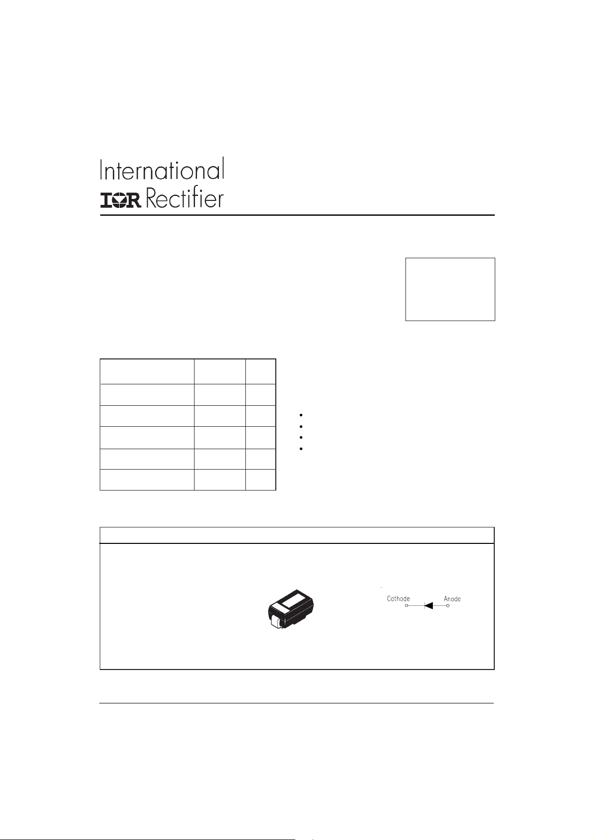
Case Styles
10MQ060N
SMA
1
10MQ060N
Bulletin PD-20519 rev. L 07/04
Voltage Ratings
Part number 10MQ060N
VRMax. DC Reverse Voltage (V)
V
Max. Working Peak Reverse Voltage (V)
RWM
60
Absolute Maximum Ratings
Parameters 10MQ Units Conditions
I
Max. Average Forward Current 1.5 A 50% duty cycle @ TL = 120 °C, rectangular wave form.
F(AV)
* See Fig. 4 On PC board 9mm2 island(.013mm thick copper pad area)
I
Max. Peak One Cycle Non-Repetitive 40 5µs Sine or 3µs Rect. pulse
FSM
A
Surge Current * See Fig. 6 10 10ms Sine or 6ms Rect. pulse
EASNon-Repetitive Avalanche Energy 2.0 mJ TJ = 25 °C, IAS = 1A, L = 4mH
IARRepetitive Avalanche Current 1.0 A
Following any rated
load condition and
with rated V
Electrical Specifications
Parameters 10MQ Units Conditions
VFMMax. Forward Voltage Drop (1) 0.63 V @ 1A
* See Fig. 1 0.71 V @ 1.5A
0.57 V @ 1A
0.63 V @ 1.5A
IRMMax. Reverse Leakage Current (1) 0.5 m A TJ = 25 °C
* See Fig. 2 7.5 mA TJ = 125 °C
V
Threshold Voltage 0.45 V TJ = TJ max.
F(TO)
rtForward Slope Resistance 86.8 mΩ
C TTypical Junction Capacitance 31 pF VR = 10VDC, TJ = 25°C, test signal = 1Mhz
L STypical Series Inductance 2.0 nH Measured lead to lead 5mm from package body
dv/dt Max. Voltage Rate of Change 10000 V/µs (Rated VR)
(1) Pulse Width < 300µs, Duty Cycle < 2%
TJ = 25 °C
TJ = 125 °C
VR = rated V
R
RRM
applied
Thermal-Mechanical Specifications
Parameters 10MQ Units Conditions
TJMax. Junction Temperature Range (*) -55 to 150 °C
T
Max. Storage Temperature Range - 55 to 150 °C
stg
R
Max. Thermal Resistance Junction 80 °C/W DC operation
thJA
to Ambient
wt Approximate Weight 0.07(0.002) g (oz.)
Case Style SMA Similar D-64
Device Marking IR1H
(*) dPtot 1
< thermal runaway condition for a diode on its own heatsink
dTj Rth( j-a)
2
www.irf.com

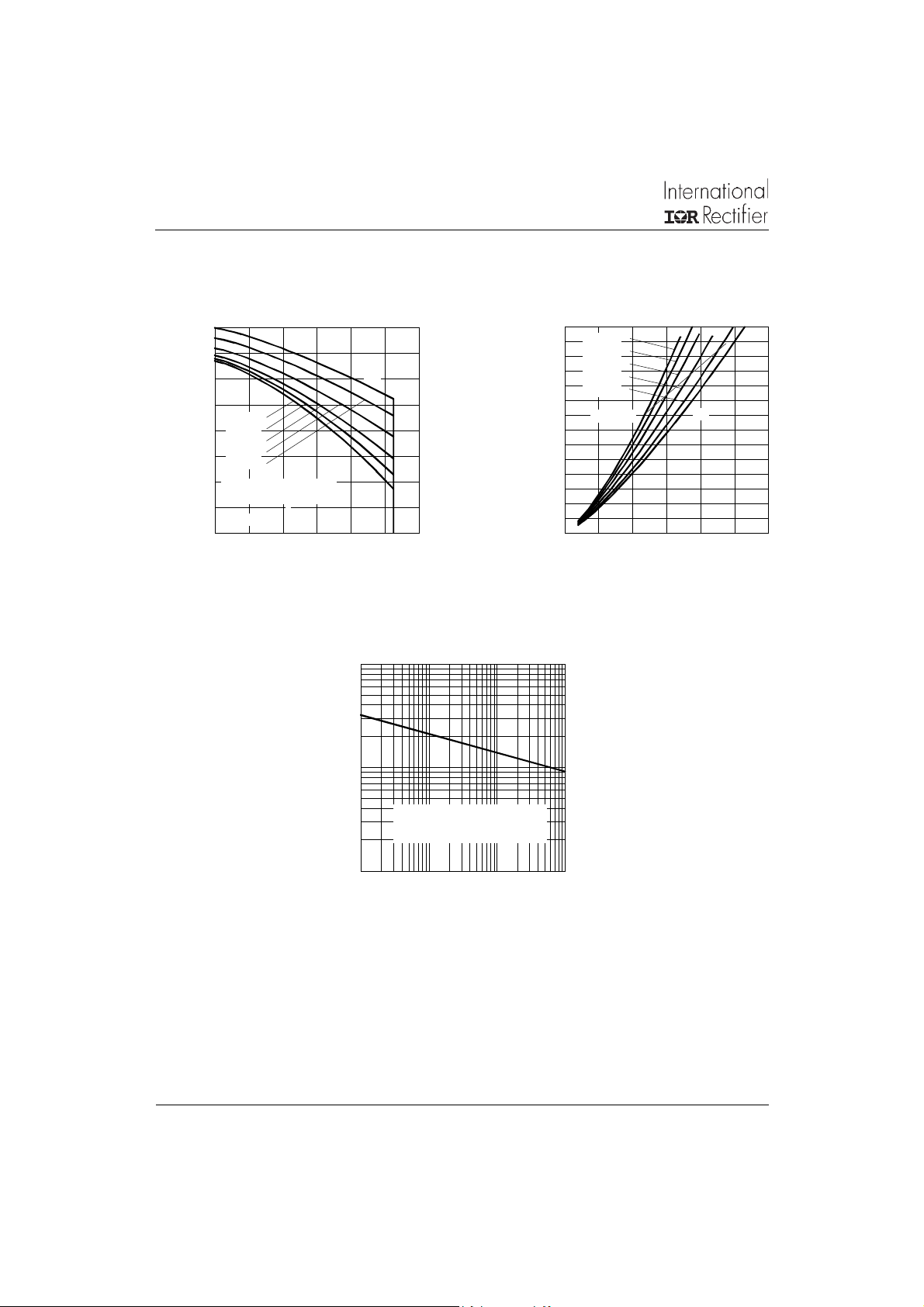
100
10MQ060N
Bulletin PD-20519 rev. L 07/04
10
T = 1 5 0° C
J
T = 1 2 5° C
J
F
T = 25° C
J
10
T = 150°C
J
R
Reverse Curre nt - I (mA )
0.0001
1
0.1
0.01
0.001
125°C
100°C
75°C
50°C
25°C
0 102030405060
Reverse Voltage - V (V)
R
Fig. 2 - Typical Peak Reverse Current
1
Instantaneous Forward Current - I (A)
100
T
Vs. Reverse Voltage
T = 25°C
J
0.1
0.20.40.60.8 1 1.21.41.6
Forward Voltage Drop - V (V)
FM
Fig. 1 - Maximum Forward Voltage Drop Characteristics
Junction Capacitance - C (pF)
10
0 102030405060
Reverse Voltage - V (V)
Fig. 3 - Typical Junction Capacitance
Vs. Reverse Voltage
R
3www.irf.com
10MQ060N
Bulletin PD-20519 rev. L 07/04
150
140
130
120
D = 0. 20
D = 0. 25
110
D = 0. 33
D = 0. 50
100
D = 0. 75
90
Squa re w a ve (D = 0.50)
80% Rated V applied
80
Allowable Case Temperature - (°C)
see note (2)
70
0 0.4 0.8 1.2 1.6 2 2.4
R
Ave rag e Forward C urrent - I (A )
Fig. 4 - Maximum Average Forward Current
Vs. Allowable Lead Temperature
100
FSM
1.4
D = 0.20
D = 0.25
1.2
0.8
D = 0.33
D = 0.50
1
D = 0.75
RM S Lim i t
DC
DC
0.6
0.4
Average Power Loss - (Watts)
0.2
0
0 0.4 0.8 1.2 1.6 2 2.4
F( A V )
Avera ge Forward Current - I (A)
F( A V )
Fig. 5 - Maximum Average Forward Dissipation
Vs. Average Forward Current
10
(2) Formula used: TC = TJ - (Pd + Pd
Pd = Forward Power Loss = I
Pd
= Inverse Power Loss = VR1 x IR (1 - D); IR @ V
REV
4
At An y Rat ed Loa d Co ndit ion
And With Rated V Applied
Follo win g Su rg e
Non-Repetitive Surge Current - I (A)
1
10 100 1000 10000
Squ a re Wave Pulse Dura t io n - t (m ic rosec )
RRM
p
Fig. 6 - Maximum Peak Surge Forward Current Vs. Pulse Duration
) x R
thJC
x VFM @ (I
;
/ D) (see Fig. 6);
F(AV)
R1
= 80% rated V
R
REV
F(AV)
www.irf.com

Outline Table
Device Marking: IR1H
10MQ060N
Bulletin PD-20519 rev. L 07/04
CATHO DE ANODE
1.40 (.055)
1.60 (.062)
2.00 (.078)
2.44 (.096)
0.76 (.030)
1.52 (.060)
4.00 (.157)
4.60 (.181)
4.80 (.188)
5.28 (.208)
2.50 (.098)
2.90 (.114)
.152 (.006)
.305 (.012)
.103 (.004)
.203 (.008)
Outline SMA
1 2
1.47 MIN.
(.058 MIN.)
SOLDER ING PAD
2
2.10 MAX .
(.085 MAX. )
5.53 (.218)
POLARIT Y PART NUMB ER
1
1.27 MIN.
(.050 MIN.)
Dimensions in millimeters and (inches)
For recommended footprint and soldering techniques refer to application note #AN-994
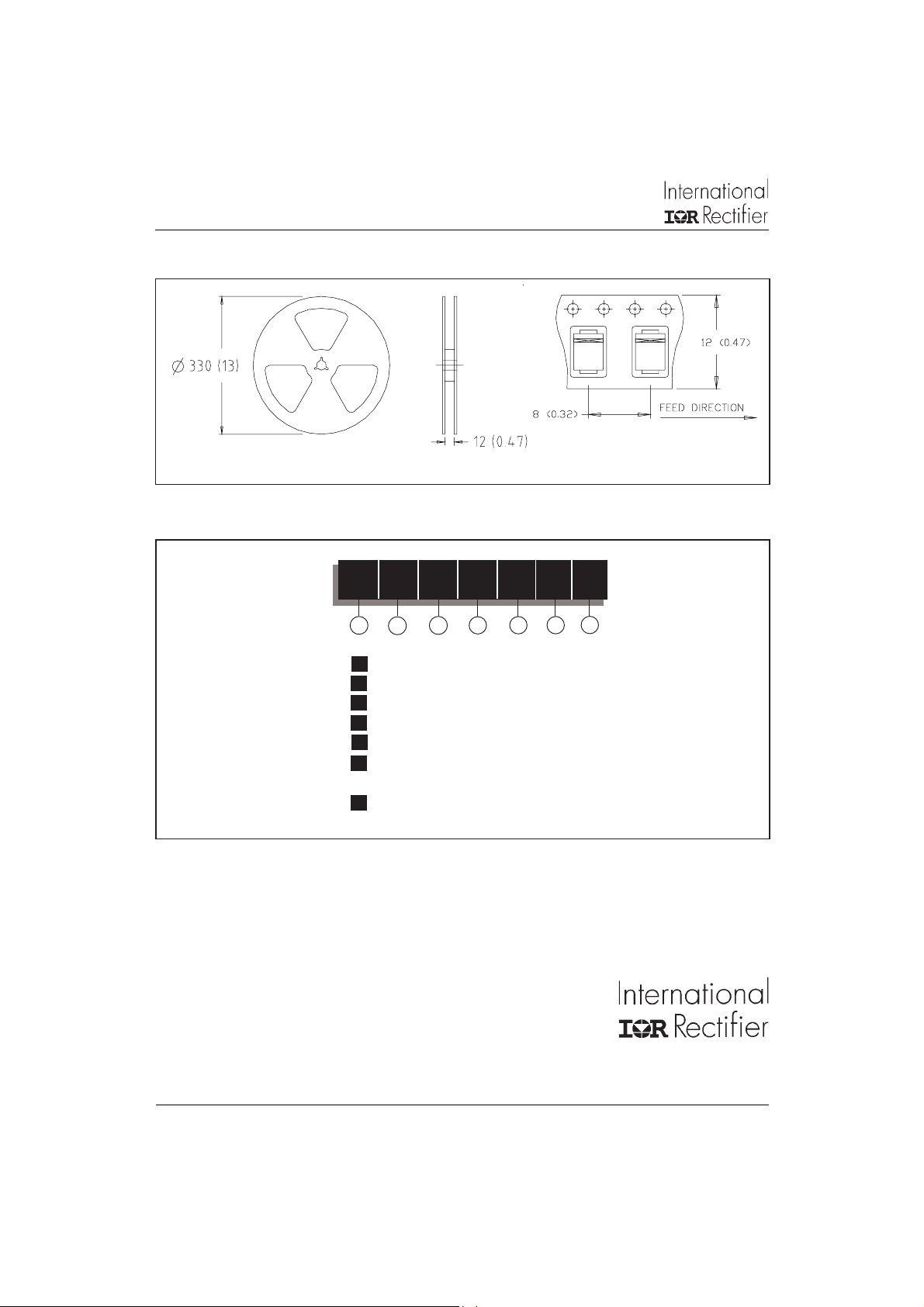
Marking & Identification
Each device has 2 rows for identification. The first row designates the device as manufactured by International
Rectifier, indicated by the letters "IR", and the Part Number (indicates the current, the voltage rating and
Schottky Generation). The second row indicates the year, the week of manufacturing and the Site ID.
IR1H
YYWWX
VOLTAGE
CURRENT
IR LOGO
SITE ID
WEEK
2nd digit of the YEAR
"Y" = 1st d igit of the YEAR "standard pr oduct"
"P" = "Lead-Free"
5www.irf.com
10MQ060N
Bulletin PD-20519 rev. L 07/04
Tape & Reel Information
Ordering Information Table
Dimensions in millimetres and (inches)
Device Code
10 M Q 060 N TR -
1
1 - Current Rating
2 - M = SMA
3 - Q = Schottky Q Series
4 - Voltage Rating (060 = 60V)
5 - N = New SMA
6 - y none= Box (1000 pieces)
3
524
y TR = Tape & Reel (7500 pieces)
7 y none = Standard Production
y PbF = Lead-Free
This product has been designed and qualified for Industrial Level.
Data and specifications subject to change without notice.
Qualification Standards can be found on IR's Web site.
7
6
IR WORLD HEADQUARTERS: 233 Kansas St., El Segundo, California 90245, USA Tel: (310) 252-7105
Visit us at www.irf.com for sales contact information. 07/04
6
TAC Fax: (310) 252-7309
www.irf.com
 Loading...