


SMA
PRODUCT SUMMARY
I
F(AV)
V
R
Schottky Rectifier, 2.1 A
Cathode Anode
2.1 A
40 V
10MQ040NPbF
Vishay High Power Products
FEATURES
• Small foot print, surface mountable
• Low forward voltage drop
• High frequency operation
• Guard ring for enhanced ruggedness and long term
reliability
• Compliant to RoHS directive 2002/95/EC
• Designed and qualified for industrial level
DESCRIPTION
The 10MQ040NPbF surface mount Schottky rectifier has
been designed for applications requiring low forward drop
and very small foot prints on PC boards. Typical applications
are in disk drives, switching power supplies, converters,
freewheeling diodes, battery charging, and reverse battery
protection.
MAJOR RATINGS AND CHARACTERISTICS
SYMBOL CHARACTERISTICS VALUES UNITS
I
F
V
I
FSM
V
T
RRM
F
J
DC 2.1 A
40 V
tp = 5 µs sine 120 A
1.5 Apk, TJ = 125 °C 0.56 V
Range - 55 to 150 °C
VOLTAGE RATINGS
PARAMETER SYMBOL 10MQ040NPbF UNITS
Maximum DC reverse voltage V
Maximum working peak reverse voltage V
R
RWM
40 V
ABSOLUTE MAXIMUM RATINGS
PARAMETER SYMBOL TEST CONDITIONS VALUES UNITS
Maximum average forward current
See fig. 4
Maximum peak one cycle
non-repetitive surge current
See fig. 6
Non-repetitive avalanche energy E
Repetitive avalanche current I
I
F(AV)
I
FSM
AS
AR
50 % duty cycle at TL = 123 °C, rectangular waveform
On PC board 9 mm
(0.013 mm thick copper pad area)
5 µs sine or 3 µs rect. pulse
10 ms sine or 6 ms rect. pulse 30
TJ = 25 °C, IAS = 1 A, L = 6 mH 3.0 mJ
Current decaying linearly to zero in 1 µs
Frequency limited by T
2
island
Following any rated
load condition and with
rated V
RRM
maximum VA = 1.5 x VR typical
J
1.5 A
120
A
applied
1.0 A
Document Number: 94117 For technical questions, contact: diodestech@vishay.com
Revision: 02-Jul-09 1
www.vishay.com

10MQ040NPbF
Vishay High Power Products
Schottky Rectifier, 2.1 A
ELECTRICAL SPECIFICATIONS
PARAMETER SYMBOL TEST CONDITIONS VALUES UNITS
1 A
Maximum forward voltage drop
See fig. 1
V
FM
1.5 A 0.62
(1)
1 A
1.5 A 0.56
Maximum reverse leakage current
See fig. 2
I
RM
Threshold voltage V
Forward slope resistance r
Typical junction capacitance C
Typical series inductance L
F(TO)
t
T
S
TJ = 25 °C
(1)
T
= 125 °C 26
J
TJ = TJ maximum
VR = 10 VDC, TJ = 25 °C, test signal = 1 MHz 38 pF
Measured lead to lead 5 mm from package body 2.0 nH
Maximum voltage rate of change dV/dt Rated V
T
= 25 °C
J
= 125 °C
T
J
V
= Rated V
R
R
R
0.54
0.49
0.5
0.36 V
104 mΩ
10 000 V/µs
Note
(1)
Pulse width < 300 µs, duty cycle < 2 %
THERMAL - MECHANICAL SPECIFICATIONS
PARAMETER SYMBOL TEST CONDITIONS VALUES UNITS
Maximum junction and
storage temperature range
Maximum thermal resistance,
junction to ambient
Approximate weight
Marking device Case style SMA (similar D-64) V1F
Note
dP
(1)
------------dT
1
tot
J
thermal runaway condition for a diode on its own heatsink
--------------<
R
thJA
(1)
T
, T
J
Stg
R
thJA
DC operation 80 °C/W
- 55 to 150 °C
0.07 g
0.002 oz.
V
mA
www.vishay.com For technical questions, contact: diodestech@vishay.com
Document Number: 94117
2 Revision: 02-Jul-09
10MQ040NPbF
Schottky Rectifier, 2.1 A
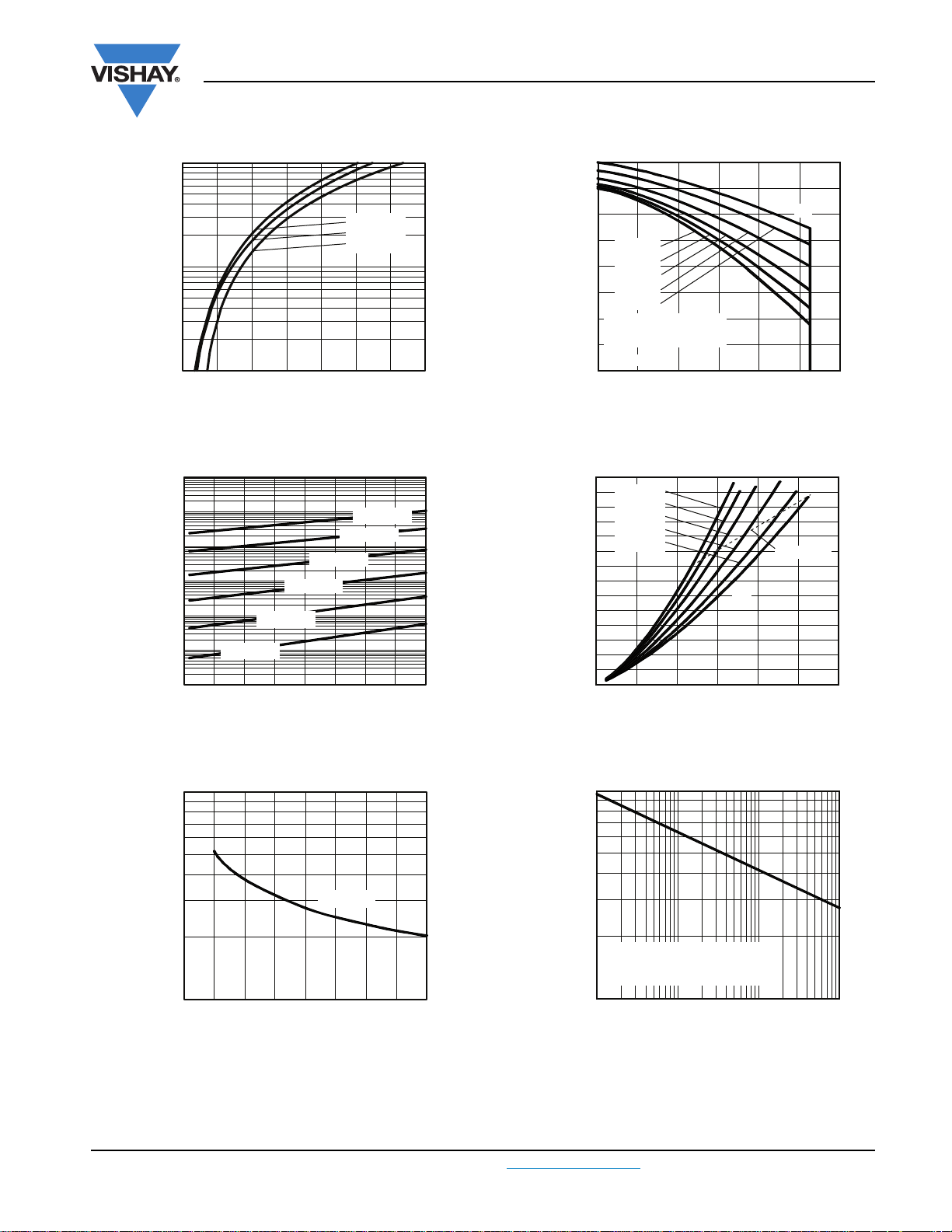
10
T
= 150 °C
J
= 125 °C
T
J
TJ = 25 °C
1
Current (A)
- Instantaneous Forward
F
I
0.1
0.2 0.4 0.6 0.8 1.6
VFM - Forward Voltage Drop (V)
Fig. 1 - Maximum Forward Voltage Drop Characteristics
100
10
1
0.1
0.01
- Reverse Current (mA)
R
0.001
I
TJ = 50 °C
TJ = 25 °C
1.0 1.2
TJ = 100 °C
TJ = 75 °C
1.4
TJ = 150 °C
TJ = 125 °C
Vishay High Power Products
150
140
130
120
D = 0.20
D = 0.25
110
D = 0.33
D = 0.50
100
D = 0.75
90
Square wave (D = 0.50)
80 % rated V
80
Allowable Case Temperature (°C)
See note (1)
70
0 0.4 0.8 1.2 2.4
I
F(AV)
Fig. 4 - Maximum Average Forward Current vs.
1.4
D = 0.20
D = 0.25
1.2
D = 0.33
D = 0.50
1.0
D = 0.75
0.8
0.6
0.4
Average Power Loss (W)
0.2
applied
R
- Average Forward Current (A)
Allowable Lead Temperature
DC
1.6 2.0
RMS limit
DC
0.0001
0
5
10 15
25
20 30
4035
VR - Reverse Voltage (V)
Fig. 2 - Typical Peak Reverse Current vs.
Reverse Voltage
100
TJ = 25 °C
- Junction Capacitance (pF)
T
C
10
0
5
15 25
20 30
4010
35
VR - Reverse Voltage (V)
Fig. 3 - Typical Junction Capacitance vs. Reverse Voltage
0
0 0.4 0.8
I
- Average Forward Current (A)
F(AV)
1.2 2.0 2.4
1.6
Fig. 5 - Maximum Average Forward Dissipation vs.
Average Forward Current
100
At any rated load condition and
with rated V
- Non-Repetitive Surge Current (A)
FSM
I
following surge
10
10
RRM
100
applied
1000
tp - Square Wave Pulse Duration (µs)
Fig. 6 - Maximum Peak Surge Forward Current vs.
Pulse Duration
10 000
Note
(1)
Formula used: TC = TJ - (Pd + Pd
Pd = Forward power loss = I
F(AV)
) x R
REV
x VFM at (I
;
thJC
/D) (see fig. 6); Pd
F(AV)
= Inverse power loss = VR1 x IR (1 - D); IR at VR1 = 80 % rated V
REV
R
Document Number: 94117 For technical questions, contact: diodestech@vishay.com
www.vishay.com
Revision: 02-Jul-09 3
10MQ040NPbF
Vishay High Power Products
ORDERING INFORMATION TABLE
Device code
10 M Q 040 N TR PbF
1 - Current rating
2 - M = SMA
3
- Q = Schottky “Q” series
4 - Voltage rating (040 = 40 V)
- N = New SMA
5
6 -
- PbF = Lead (Pb)-free
7
Schottky Rectifier, 2.1 A
51324
None = Box (1000 pieces)
TR = Tape and reel (7500 pieces)
67
LINKS TO RELATED DOCUMENTS
Dimensions www.vishay.com/doc?95018
Part marking information www.vishay.com/doc?95029
Packaging information www.vishay.com/doc?95034
SPICE model www.vishay.com/doc?95277
www.vishay.com For technical questions, contact: diodestech@vishay.com
4 Revision: 02-Jul-09
Document Number: 94117

Legal Disclaimer Notice
Vishay
Disclaimer
All product specifications and data are subject to change without notice.
Vishay Intertechnology, Inc., its affiliates, agents, and employees, and all persons acting on its or their behalf
(collectively, “Vishay”), disclaim any and all liability for any errors, inaccuracies or incompleteness contained herein
or in any other disclosure relating to any product.
Vishay disclaims any and all liability arising out of the use or application of any product described herein or of any
information provided herein to the maximum extent permitted by law. The product specifications do not expand or
otherwise modify Vishay’s terms and conditions of purchase, including but not limited to the warranty expressed
therein, which apply to these products.
No license, express or implied, by estoppel or otherwise, to any intellectual property rights is granted by this
document or by any conduct of Vishay.
The products shown herein are not designed for use in medical, life-saving, or life-sustaining applications unless
otherwise expressly indicated. Customers using or selling Vishay products not expressly indicated for use in such
applications do so entirely at their own risk and agree to fully indemnify Vishay for any damages arising or resulting
from such use or sale. Please contact authorized Vishay personnel to obtain written terms and conditions regarding
products designed for such applications.
Product names and markings noted herein may be trademarks of their respective owners.
Document Number: 91000 www.vishay.com
Revision: 18-Jul-08 1
 Loading...