

Bulletin PD-2.437 rev. H 07/04
10BQ100
SCHOTTKY RECTIFIER
Major Ratings and Characteristics
Characteristics 10BQ100 Units
I
Rectangular waveform 1.0 A
F(AV)
V
RRM
I
@ tp = 5 µs sine 780 A
FSM
VF@ 1.0 Apk, TJ=125°C 0.62 V
TJrange - 55 to 175 °C
100 V
1 Amp
I
= 1 Amp
F(AV)
VR = 100V
Description/ Features
The 10BQ100 surface-mount Schottky rectifier has been
designed for applications requiring low forward drop and very
small foot prints on PC boards. Typical applications are in disk
drives, switching power supplies, converters, free-wheeling
diodes, battery charging, and reverse battery protection.
Small foot print, surface mountable
Low forward voltage drop
High frequency operation
Guard ring for enhanced ruggedness and long term
reliability
www.irf.com
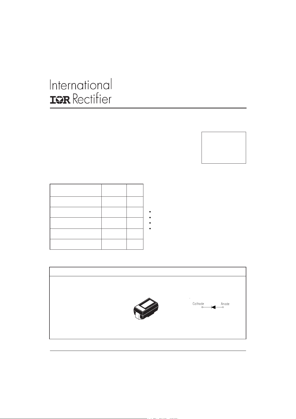
Case Styles
10BQ100
SMB
1
10BQ100
Bulletin PD-2.497 rev. H 07/04
Voltage Ratings
Part number 10BQ100
VRMax. DC Reverse Voltage (V)
V
Max. Working Peak Reverse Voltage (V)
RWM
100
Absolute Maximum Ratings
Parameters 10BQ Units Conditions
I
Max. Average Forward Current 1.0 A 50% duty cycle @ TL = 152 °C, rectangular wave form
F(AV)
I
Max. Peak One Cycle Non-Repetitive 7 80 A 5µs Sine or 3µs Rect. pulse
FSM
Surge Current 38 10ms Sine or 6ms Rect. pulse
EASNon- Repetitive Avalanche Energy 1.0 mJ TJ = 25 °C, IAS = 0.5A, L = 8mH
IARRepetitive Avalanche Current 0.5 A Current decaying linearly to zero in 1 µsec
Frequency limited by TJ max. Va = 1.5 x Vr typical
Following any rated
load condition and
with rated V
RRM
applied
Electrical Specifications
Parameters 10BQ Units Conditions
VFMMax. Forward Voltage Drop (1) 0.78 V @ 1A
* See Fig. 1 0.89 V @ 2A
0.62 V @ 1A
0.72 V @ 2A
IRMMax. Reverse Leakage Current (1) 0.5 mA TJ = 25 °C
* See Fig. 2 1 mA TJ = 125 °C
CTTypical Junction Capacitance 42 pF VR = 5VDC, (test signal range 100kHz to 1MHz) 25°C
LSTypical Series Inductance 2.0 nH Measured lead to lead 5mm from package body
dv/dt Max. Volatge Rate of Charge 10000 V/ µs
(Rated VR)
(1) Pulse Width < 300µs, Duty Cycle < 2%
TJ = 25 °C
TJ = 125 °C
VR = rated V
R
Thermal-Mechanical Specifications
Parameters 10BQ Units Conditions
TJMax. Junction Temperature Range (*) - 55 to 175 °C
T
Max. Storage Temperature Range - 55 to 175 °C
stg
R
Max. Thermal Resistance Junction 36 °C/W DC operation
thJL
to Lead (**)
R
Max. Thermal Resistance Junction 80 °C/W
thJA
to Ambient
wt Approximate Weight 0.10 (0.003) g (oz.)
Case Style SMB Similar DO-214AA
Device Marking IR1J
(*) dPtot 1
< thermal runaway condition for a diode on its own heatsink
dTj Rth( j-a)
(**) Mounted 1 inch square PCB
2
www.irf.com
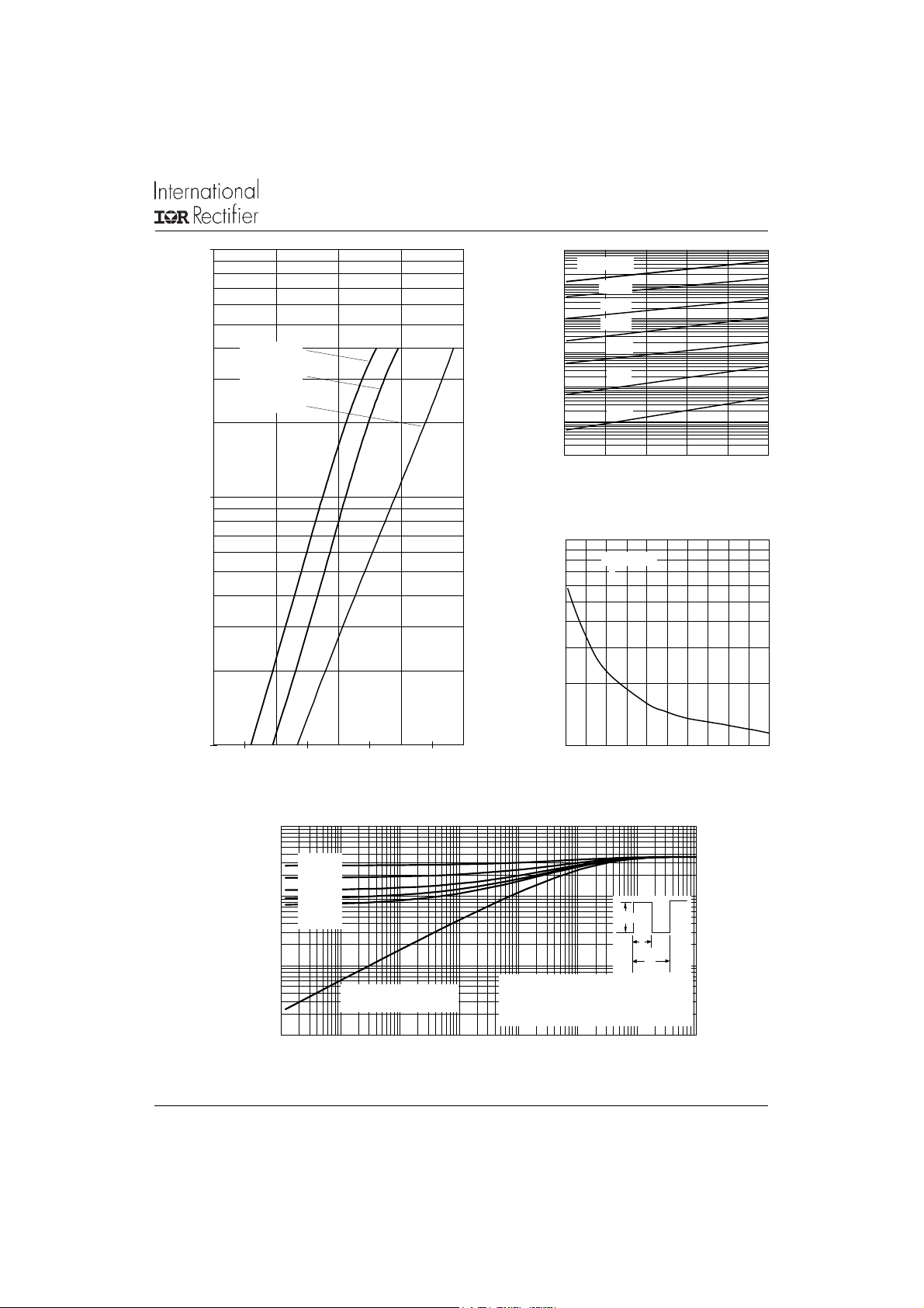
10
0.00001
0.0001
0.001
0.01
0.1
1
10
0 20406080100
75˚C
25˚C
Tj = 175˚C
150˚C
125˚C
100˚C
50˚C
Tj = 175˚C
Tj = 125˚C
(mA)
R
10BQ100
Bulletin PD-2.497 rev. H 07/04
(A)
F
Tj = 25˚C
1
Instantaneous Forward Current - I
0.1
0.2 0.4 0.6 0.8 1
Forward Voltage Drop - VFM (V)
Fig. 1 - Maximum Forward Voltage Drop Characteristics
100
Reverse Current - I
Reverse Voltage - VR (V)
Fig. 2 - Typical Peak Reverse Current
Vs. Reverse Voltage
100
T = 25˚C
J
(p F)
T
Junction Capacitance - C
10
0 20406080100
Reverse Voltage - VR (V)
Fig. 3 - Typical Junction Capacitance
Vs. Reverse Voltage
(°C/W)
thJC
10
D = 0.50
D = 0.33
D = 0.25
D = 0.20
P
DM
1
D = 0.75
Notes:
1. Duty factor D = t1/ t2 .
2. Peak Tj = Pdm x ZthJC + Tc .
Thermal Impedance Z
(Thermal Resistance)
Single Pulse
0.1
0.00001 0.0001 0.001 0.01 0.1 1 1 0 100
t1 , Rectangular Pulse Duration (Seconds)
Fig. 4 - Max. Thermal Impedance Z
Characteristics (Per Leg)
thJC
t
1
t
2
3www.irf.com

10BQ100
Bulletin PD-2.497 rev. H 07/04
180
170
DC
160
150
140
Square wave (D = 0.50)
130
Rated Vr applied
120
Allowable Lead Temperature (°C)
see note (2)
110
0 0.4 0.8 1.2 1.6
Average Forward Current - I
Fig. 4 - Maximum Average Forward Current
Vs. Allowable Lead Temperature
1000
FSM
100
(A)
D = 0.20
D = 0.25
D = 0.33
D = 0.50
D = 0.75
F(AV)
(A)
1
D = 0.20
D = 0.25
D = 0.33
0.8
D = 0.50
D = 0.75
0.6
RMS Limit
0.4
0.2
Average Power Loss (Watts)
DC
0
0 0.3 0.6 0.9 1.2 1.5
Average Forward Current - I
F(AV)
Fig. 5 - Maximum Average Forward Dissipation
Vs. Average Forward Current
(A)
Fig. 6 - Maximum Peak Surge Forward Current Vs. Pulse Duration
(2) Formula used: TC = TJ - (Pd + Pd
Pd = Forward Power Loss = I
Pd
= Inverse Power Loss = VR1 x IR (1 - D); IR @ V
REV
4
At Any Rated Load Condition
And With rated Vrrm Applied
Following Surge
Non-Repetitive Surge Current - I
10
10 100 1000 10000
Square Wave Pulse Duration - T
) x R
thJC
x VFM @ (I
;
/ D) (see Fig. 6);
F(AV)
R1
= 80% rated V
REV
F(AV)
R
(Microsec)
p
www.irf.com

Outline Table
10BQ100
Bulletin PD-2.497 rev. H 07/04
Device Marking: IR1J
2.15 (.085)
1.80 (.071)
2.40 (.094)
1.90 (.075)
1.30 (.051)
0.76 (.030)
4.70 (.185)
4.10 (.161)
5.60 (.220)
5.00 (.197)
3.80 (.150)
3.30 (.130)
0.30 (.012)
0.15 (.006)
CATHODE A NODE
1 2
2.5 TYP.
2
PART NUMBER
SOLDERING PAD
4.2 (.165)
4.0 (.157)
POLARITY
1
(.098 TYP.)
2.0 TYP.
(.079 TYP.)
Outline SMB
Dimensions in millimeters and (inches)
For recommended footprint and soldering techniques refer to application note #AN-994
Marking & Identification
Each device has 2 rows for identification. The first row designates the device as manufactured by International
Rectifier, indicated by the letters "IR", and the Part Number (indicates the current, the voltage rating and
Schottky Generation). The second row indicates the year, the week of manufacturing and the Site ID.
IR1J
YYWWX
VOLTAGE
CURRENT
IR LOGO
SITE ID
WEEK
2nd digit of the YEAR
"Y" = 1st d igit of the YEAR "standard product "
"P" = "Lea d-Free"
5www.irf.com

10BQ100
Bulletin PD-2.497 rev. H 07/04
Tape & Reel Information
Ordering Information Table
Dimensions in millimetres and (inches)
Device Code
10 B Q 100 TR -
524
1
1 - Current Rating
2 - B = Single Lead Diode
3 - Q = Schottky Q Series
4 - Voltage Rating (100 = 100V)
5 - y none= Box (1000 pieces)
3
y TR = Tape & Reel (3000 pieces)
6 y none = Standard Production
y PbF = Lead-Free
10BQ100
********************************************************************************
* SPICE Model Diode *
********************************************************************************
.SUBCKT 10BQ100 ANO CAT
D1 ANO 1 CAT
*Define diode model
.model D10BQ100 D(Is=341.4E-06 N=2.664 Rs=3.65E-03 Ikf=37.08E-03 Xti=2 Eg=1.11
+ Cjo=65.57E-12 M=.5751 Vj=4.282 Fc=0.5 Isr=17.26E-27 Nr=5.662
+ Bv=119.9 Ibv=215.5E-06 Tt=43.28E-09)
********************************************************************************
.ENDS 10BQ100
6
6
www.irf.com

10BQ100
Bulletin PD-2.497 rev. H 07/04
This product has been designed and qualified for Industrial Level.
Data and specifications subject to change without notice.
Qualification Standards can be found on IR's Web site.
IR WORLD HEADQUARTERS: 233 Kansas St., El Segundo, California 90245, USA Tel: (310) 252-7105
TAC Fax: (310) 252-7309
Visit us at www.irf.com for sales contact information. 07/04
7www.irf.com
 Loading...