

Viking Technology PSFDUC3XXXXYXX User Manual

Manual
9/16/2014
Revision B
Page 1 of 18
Viking eUSB
Embedded USB Manual
~
Industrial Products
PSFDUC3XXXXYXX Viking Technology
www.vikingtechnology.com
Manual
9/16/2014
Revision B
Page 2 of 18
Date
Revision
Description
B
9/16/14
Add VRFDUC31024YCG PN.
Revision History
Initial release VRFDUC3(L)032GYCNxx PN for SM3252
VRFDUC3032GYCNE1 (12/13/2013)
Update PN table for new PN’s and 16GB (A1, 6/2/2014)
A 9/12/14
Revised Standby Current and Operating Current based on 3.3V
NAND devices (A2, 7/8/14)
Removed firmware upgrade capability (A3, 8/8/14)
PSFDUC3XXXXYXX Viking Technology
www.vikingtechnology.com

Manual
9/16/2014
Revision B
Page 3 of 18
Legal Information
Legal Information
Copyright© 2014 Sanmina Corporation. All rights reserved. The information in
this document is proprietary and confidential to Sanmina Corporation. No part of
this document may be reproduced in any form or by any means or used to make
any derivative work (such as translation, transformation, or adaptation) without
written permission from Sanmina. Sanmina reserves the right to revise this
documentation and to make changes in content from time to time without
obligation on the part of Sanmina to provide notification of such revision or
change.
Sanmina provides this documentation without warranty, term or condition of any
kind, either expressed or implied, including, but not limited to, expressed and
implied warranties of merchantability, fitness for a particular purpose, and noninfringement. While the information contained herein is believed to be accurate,
such information is preliminary, and should not be relied upon for accuracy or
completeness, and no representations or warranties of accuracy or
completeness are made. In no event will Sanmina be liable for damages arising
directly or indirectly from any use of or reliance upon the information contained in
this document. Sanmina may make improvements or changes in the product(s)
and/or the program(s) described in this documentation at any time.
Sanmina, Viking Technology, Viking Modular Solutions, and the Viking logo are
trademarks of Sanmina Corporation. Other company, product or service names
mentioned herein may be trademarks or service marks of their respective
owners.
PSFDUC3XXXXYXX Viking Technology
www.vikingtechnology.com
Manual
9/16/2014
Revision B
Page 4 of 18
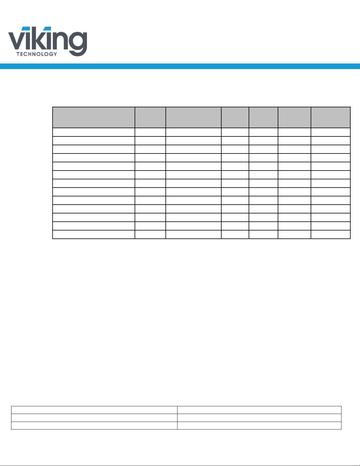
Part Number
( four flash placements)
Capacity
Device Density
Voltage
Devices
Channels
LBA
VRFDUC3(L)1024YCGyy
Ordering Information: eUSB Family
Viking High Performance USB embedded Drive Ordering Information
Version-1
VRFDUC3(L)1024YxE3yy 1GB 8Gb 3.3 1 2 1,974,672
VRFDUC3(L)2048YxE3yy 2GB 8Gb 3.3 2 2 3,928,176
VRFDUC3(L)4096YxH3yy 4GB 16Gb 3.3 2 2 7,835,184
VRFDUC3(L)8192YxK3yy 8GB 32Gb 3.3 2 2 15,649,200
VRFDUC3(L)016GYxK3yy 16GB 32Gb 3.3 4 2 31,277,232
VRFDUC3(L)032GYxN3yy 32GB 64Gb 3.3 4 2 62,533,296
1GB 8Gb 5 1 1 1,974,672
VRFDUC3(L)2048YxGyy 2GB 8Gb 5 2 2 3,928,176
VRFDUC3(L)4096YxHyy 4GB 16Gb 5 2 2 7,835,184
VRFDUC3(L)8192YxKyy 8GB 32Gb 5 2 2 7,835,184
VRFDUC3(L)016GYxKyy 16GB 32Gb 5 4 2 31,277,232
VRFDUC3(L)032GYxNyy 32G 64Gb 5 4 2 62,533,296
Notes:
1. DUC3xxxx signifies standard profile, DUC3Lxxxx signifies low profile.
2. x = C for Commercial temperature range: 0 to 70°C (32 to 158° F)
or I for Industrial temperature range: -40 to 85°C (-40 to 185° F)
3. Storage capacity listed will vary due to formatting and additional functions,
and therefore is not available for storage.
4. USB’s ship formatted from the factory unless otherwise requested.
5. All eUSBs are based on SLC flash unless otherwise requested.
6. All capacities are available in 3.3V version s.
7. yy indicates BOM specific information
8. “L” indicate low profile
9. Maximum of 4KB per page
#
PSFDUC3XXXXYXX Viking Technology
www.vikingtechnology.com

Manual
9/16/2014
Revision B
Page 5 of 18
Table of Contents
1 INTRODUCTION 7
1.1 Product Overview 7
1.2 Features 7
1.3 Block Diagram 8
1.4 USB Interface 9
2 PRODUCT SPECIFICATIONS 9
2.1 Performance 9
2.2 Timing 9
2.3 Power-up AC timing Requirements 9
2.4 Electrical Characteristics 10
2.4.1 Absolute Maximum Ratings 10
2.4.2 DC Operating Conditions and Characteristics 10
2.4.3 Power Consumption 10
2.4.4 Capacitance 11
2.5 Environmental Conditions 11
2.5.1 Temperature and Altitude 11
2.6 Reliability 11
3 MECHANICAL INFORMATION 13
4 PIN AND SIGNAL DESCRIPTIONS 17
4.1 Signal and Power Description Tables 17
5 CERTIFICATIONS AND COMPLIANCE 18
6 REFERENCES 18
PSFDUC3XXXXYXX Viking Technology
www.vikingtechnology.com

Manual
9/16/2014
Revision B
Page 6 of 18
Table of Tables
Table 2-1: Maximum Sustained Read and Write Bandwidth _____________________________ 9
Table 2-2: Timing Specifications __________________________________________________ 9
Table 2-3: Absolute Maximum Ra tin gs ____________________________________________ 10
Table 2-4: Voltage and Curr ent Ratin gs ____________________________________________ 10
Table 2-5: Power Consumption __________________________________________________ 11
Table 2-6: Bus Line Capacitance _________________________________________________ 11
Table 2-7: Temperature and Altitude Related Specifications ____________________________ 11
Table 2-8: Reliability Spec if icati ons _______________________________________________ 11
Table 4-1: eUSB Connector Pin Signal Definitions ___________________________________ 17
Table 5-1: Device Certifications __________________________________________________ 18
Table of Figures
Figure 1-1: High-Level Block Diagram ______________________________________________ 8
Figure 3-1: Location of PCB # marking ____________________________________________ 13
Figure 3-2: Dimensions (Version-1) _______________________________________________ 14
Figure 3-3: Dimensions (Version-2, low profile) ______________________________________ 15
Figure 3-4: Dimensions (Version 2, standard profile) __________________________________ 16
Figure 4-1: Connector Pin Assignments ____________________________________________ 17
PSFDUC3XXXXYXX Viking Technology
www.vikingtechnology.com
 Loading...