


C O M P U T E R S N E T W O R K S S O L U T I O N S
..
VIG556M
Motherboard
Manual

V1.0 VIG556M Motherboard Manual
1
Viglen, EMC and the ‘CE’ mark
CE Marking
European standards are being harmonised across borders. If products comply with the same standards in all
European countries, product exporting and importing is made simple - paving our way to a common market. If
you buy a product with a 'CE' mark on it (shown below), on the box, in the manual, or on the guarantee - it
complies with the currently enforced directive(s).
Introduction to EMC
EMC (Electromagnetic Compatibility) is the term used to describe certain issues with RF (Radio Frequency)
energy. Electrical items should be designed so they do not interfere with each other through RF emissions. E.g.
If you turn on your microwave, your television shouldn't display interference if both items are CE marked to the
EMC directive.
If emitted RF energy is not kept low, it can interfere with other electrical circuitry - E.g. Cars Automatic Braking
Systems have been known to activate by themselves while in a strong RF field. As this has obvious
repercussions ALL electrical products likely to cause RF related problems have to be 'CE' marked from 1st
January 1996 onwards.
If a product conforms to the EMC directive, not only should its RF emissions be very low, but its immunity to RF
energy (and other types) should be high. The apparatus has to resist many 'real world' phenomena such as
static shocks and mains voltage transients.
Viglen’s Environment laboratory
To gain a 'CE' mark, the Viglen computer range has had to undergo many difficult tests to ensure it is
Electromagnetically Compatible. These are carried out in the in-house 'Environment lab' at Viglen Headquarters.
We have made every effort to guarantee that each computer leaving our factory complies fully with the correct
standards. To ensure the computer system maintains compliance throughout its functional life, it is essential you
follow these guidelines.
¾ Install the system according to Viglen’s instructions
¾ If you open up your Viglen:
¾ Keep internal cabling in place as supplied.
¾ Ensure the lid is tightly secured afterwards
¾ Do not remove drive bay shields unless installing a 'CE' marked peripheral in its place
¾ The clips or ‘bumps' around the lips of the case increase conductivity - do not remove or damage.
¾ Do not remove the ferrite ring from the L.E.D cables.
¾ Only use your Viglen computer with 'CE' marked peripherals
This system has been tested in accordance with European standards for use in residential and light industrial
areas-this specifies a 10 meter testing radius for emissions and immunity. If you do experience any adverse
affects which you think might be related to your computer, try moving it at least 10 meters away from the affected
item. If you still experience problems, contact Viglen’s Technical Support department who will put you straight
through to an EMC engineer - s/he will do everything possible to help. If modifications are made to your Viglen
computer system, it might breach EMC regulations. Viglen take no responsibility (with regards to EMC
characteristics) of equipment which has been tampered with or modified.
This symbol on the product or on its packaging indicates that the product shall not be treated as
household waste. Instead it shall be handed over to the applicable collection point for recycling of
electrical and electronic equipment. By ensuring this product is disposed of correctly, you will help
prevent potential negative consequences for the environment and human health, which could
otherwise be caused by inappropriate waste handling of this product. The recycling of materials will
help to conserve natural resources. For more detailed information about recycling of this product,
please contact your local city office, your household waste disposal service or Viglen Ltd.

V1.0 VIG556M Motherboard Manual
2
Copyrights and Trademarks
Please note
The material in this manual is subject to change without notice.
Trademarks
Microsoft, Windows, Windows NT, Windows 95,Windows 98, Windows ME,
Windows 2000 Pro, Windows XP Pro and MS-DOS are registered trademarks of
Microsoft Corporation. IBM PC, XT, AT and PS/2 are trademarks of International
Business Machines Corporation. Pentium® and Pentium® Pro are registered
trademarks of Intel® Corporation. All other trademarks are acknowledged. JAC-UP,
Genie, Contender, Dossier, Vig, Viglen, and Envy are trademarks of Viglen Limited.
Copyright and Patents
This manual and all accompanying software and documentation are copyrighted and
all rights reserved. This product, including software and documentation, may not, in
whole or in part, be copied, photocopied, translated or reduced to any electronic or
machine-readable form, without prior written consent except for copies retained by
the purchaser for backup.
© Copyright 2006 Viglen Limited
All Rights Reserved
VIG556M Manual Version 1.0
Printed in the United Kingdom
Liability
No warranty or representation, either expressed or implied, is made with respect to
this documentation, its quality, performance, merchantability or fitness for a particular
purpose. As a result the documentation is licensed as is, and you, the licensee, are
assuming the entire risk as to its quality and performance. The vendor reserves the
right to revise this operation manual and all accompanying software and
documentation and to make changes in the content without obligation to notify any
person or organisation of the revision or change.
In no event will the vendor be liable for direct, indirect, special, incidental or
consequential damages arising out of the use or inability to use this product or
documentation, even if advised of the possibility of such damages. In particular, the
vendor shall not have liability for any hardware, software or data stored or used with
the product, including the costs of repairing, replacing or recovering such hardware,
software or data.

V1.0 VIG556M Motherboard Manual
3
Contents
Chapter 1: Motherboard Overview 5
Introduction 5
Feature Summary 6
System Board Components 14
Overview of System Board Components 15
Back Panel Connectors 18
Chapter 2: System Board Options 20
Overview of Jumper Settings 22
System Board Jumper Settings 23
Motherboard Connectors 25
Front Panel Connectors 26
Upgrading the CPU 27
Installing & Removing Memory Modules 28
Expansion Slots (PCI & AGP) 29
Replacing the Clock/CMOS RAM Battery 31
Chapter 3: Solving Problems 32
Resetting the System 32
Troubleshooting Procedures 33
Problems Operating Add-in Boards 34
Problems & Suggestions 35
Chapter 4: System BIOS 37
What is the BIOS? 37
The Power-On Sequence 37
Phoenix BIOS – Introduction 38
BIOS Upgrades 38
Using AWDFALSH to Update the BIOS 38
Configuring the Motherboard using BIOS Setup 40
BIOS Setup Program 41
Main Menu 42
Main Menu items 42
Main BIOS Menu Screen 43
Standard CMOS Features 45
Advanced BIOS Features 47

V1.0 VIG556M Motherboard Manual
4
Advanced Chipset Features 49
DRAM Timing Control 50
AGP & P2P Bridge Control 51
OnChip AGP Control 52
VGA Share Memory Size 52
Integrated Peripherals 53
OnChip PCI Device 54
OnChip IDE Device 55
Onboard Super I/O Device 56
Power Management Setup 57
PM Wakeup Events 58
PnP/PCI Configurations 59
IRQ Resources 60
PC Health Status 62
Frequency/Voltage Control 63
Main Menu Additional Options 64
Chapter 5: Technical Information 65
Enhanced IDE 65
Operating Systems and Hard Drives 65
Power Supply Connector 67
Other Useful Connectors 67
Other Information 71
Reliability 71
Temperature 71
Chapter 6: Glossary 72
Notes 74
Chapter 7: Suggestions 75

V1.0 VIG556M Motherboard Manual
5
Chapter 1: Motherboard Overview
Introduction
This manual describes the Viglen Vig556M motherboard inside your computer. The
motherboard is the most important part of your computer. It contains all of the CPU,
memory and graphics circuitry that make the computer work.
The motherboard contains the very latest CPU design that supports the Intel®
Pentium® 4 & Pentium® D family including Hyper-Threading enabled CPU’s and the
very latest Dual Core CPU’s. All of the supported CPU’s include Intel’s® MMX
Technology. MMX technology adds a total of 57 new instructions to the CPU, all of
which are designed to vastly improve both multimedia and communications on your
PC. The combination of the Intel® processor, MMX technology and Viglen expertise
make this a formidable computer.
This manual contains technical information about the Viglen Vig556M motherboard
and other hardware components inside your computer. If you are new to computers
we recommend that you read the user guide first. If you are an experienced
computer user this manual should provide all the information you will need to
perform simple upgrades and maintenance.
We hope that this manual is both readable and informative. If you have any
comments for suggestions about how we could improve the format then please fill
out the form at the back of the manual and send it to us.
Above all we hope that you enjoy using your Viglen computer.

V1.0 VIG556M Motherboard Manual
6
Feature Summary
The Vig556M motherboard supports Intel® Pentium® 4 & Pentium® D processors
with up to 2MB of second-level cache integrated in an LGA 775 Socket package
operating at speeds of up to 3.6GHz. Also supported is the Intel® Celeron® D
processor 775 pin with up to 512K second-level cache and a 533MHz system bus
operating at speeds of up to 3.46GHz.
The motherboard features:
Form factor:
• Micro ATX Form Factor: 243mm by 230mm
Processor:
• Single Celeron® D/Pentium® 4/Pentium® D CPU
• 400MHz Quad-pumped bus
• Integrated up to 2MB second-level cache (CPU dependant)
• Socket 775 connector
Main memory:
• Two 184-pin DDR DIMM sockets.
• Support for up to 2GB of DDR DIMM memory.
Chipset
• SiS 661FX
• 800Hz Front Side Bus (FSB)
• AGP 8x
• Support for 266/333/400MHz DDR RAM
• Advanced System Power Management features
• Integrated Super I/O Controller
• DirectSound AC97 Audio
• Dual bus master IDE Ultra DMA33/66/100/133
Audio
Audio Codec ’97 (AC ’97) compatible audio subsystem
LAN
Realtek 10/100 Mbit/sec Platform LAN Connect (PLC) device

V1.0 VIG556M Motherboard Manual
7
Peripheral Interfaces
• Support for two internal Universal Serial Bus (USB) ports and four external
• One serial port
• One parallel port
• Two IDE interfaces with Ultra DMA 33, ATA66/100/133 support.
• Two SATA interfaces.
• One diskette drive interface
• PS/2 keyboard and mouse ports
Expansion Capabilities
• Three PCI bus add-in card connectors
• One AGP Pro connector
Instantly Available PC
• Support for PCI Local Bus Specification Revision 2.2
• Suspend to RAM support
• Wake on PS/2 keyboard and USB ports
Wake on LAN Technology Connector
• Support for system wake up using an add-in network interface card with
remote wake up capability
Microprocessor
The motherboard supports a single Celeron D, Pentium 4 or Pentium D processor.
The processor’s VID pins automatically program the voltage regulator on the
motherboard to the required processor voltage. In addition, the front side bus speed
is automatically selected. The motherboard currently supports processors that run
internally up to 3.6GHz and have up to a 2MB second-level cache running at full
CPU Speed.
The processor implements MMX ™ technology and maintains full backward
compatibility with the 8086, 80286, Intel386 ™, Intel486 ™, Pentium, Pentium Pro,
Pentium II & Pentium III processors. The processor’s numeric coprocessor
significantly increases the speed of floating-point operations and complies with
ANSI/IEEE standard 754-1985.
Microprocessor Packaging
The Pentium 4/D processor comes in an LGA package that connects to the
motherboard through a socket 775 connector. The package consists of:
• Processor card including the processor core and the second-level cache,
burst pipelined synchronous static RAM (BSRAM) and tag RAM.
• Thermal plate.
• Back cover.

V1.0 VIG556M Motherboard Manual
8
Second Level Cache
The second-level cache is located on the die of the CPU itself. The cache includes
burst pipelined synchronous static RAM (BSRAM) and tag RAM. All supported
onboard memory can be cached.
Processor Upgrades
The motherboard can be upgraded with a Pentium 4 or Pentium D processor that
runs at higher speeds.
Memory
Main Memory
The motherboard has two DDR DIMM sockets. Minimum memory size is 128MB;
maximum memory size is 2GB. The BIOS automatically detects memory type, size,
and speed.
The motherboard supports the following memory features:
• 184-pin DIMMs.
• 266/333/400Mhz
• Un-Buffered Non-ECC DIMM.
RDRAM
Synchronous DRAM (SDRAM) improves memory performance through memory
access that is synchronous with the memory clock. This simplifies the timing design
and increases memory speed because all timing is dependent on the number of
memory clock cycles.
Chipset
The SiS 661FX chipset is the latest generation of desktop PCI set, it includes new
features such as –
• 8x AGP Support
• ATA-133 IDE Hard drive support
• SATA Hard drive support
• 800MHz Front Size Bus support
• ACPI & On-Now

V1.0 VIG556M Motherboard Manual
9
Accelerated Graphics Port (AGP)
The Vig556M features both integrated graphics and an AGP port. When using the
integrated graphics then a dynamic portion of the main system memory is used as
video memory. You can also use any AGP video card, with 4x/8x AGP performance.
The Accelerated Graphics Port (AGP) is a high-performance interconnect for
graphic-intensive applications, such as 3D applications. AGP is independent of the
PCI bus and is intended for exclusive use with graphical-display devices. AGP
overcomes certain limitations of the PCI bus related to handling a large amount of
graphics data with the following performance features:
• Pipelined-memory read and write operations that hide memory access
latency.
• Demultiplexing of address and data on the bus for near 100 percent bus
efficiency.
• AC timing for 133 MHz data transfer rates, allowing data throughput of 500
MB/sec.
Realtek 8100C Platform LAN Connect Device
The Realtek 8100C component provides an interface to the back panel RJ-45
connector with integrated LEDs. This physical interface may alternately be provided
via the CNR connector.
The Realtek 8100C provides the following functions:
• Basic 10/100 Ethernet LAN Connectivity
• Supports RJ-45 connector with status indicator LEDs
• Full driver compatibility
• Advanced Power Management support
• Programmable transit threshold
• Configuration EEPROM that contains the MAC address
RJ-45 LAN Connector LEDs
Two LEDs are built into the RJ-45 LAN connector. The following table describes the
LED states when the board is powered up and the LAN subsystem is operating.
Table 1: LAN LED Status
LED Colour LED State Condition
Green Off 10 Mbit/sec data rate is
selected.
Green On 100 Mbit/sec date rate is
selected.
Yellow Off LAN link is not
established.
Yellow On (steady state) LAN link is established.
Yellow On (brighter and pulsing) The computer is
communicating with
another computer on
the LAN.
Universal Serial Bus (USB)
The motherboard has four USB ports and a further four can be added via internal
headers; one USB peripheral can be connected to each port. For more than eight

V1.0 VIG556M Motherboard Manual
10
USB devices, an external hub can be connected to either port. The motherboard
fully supports the universal host controller interface (UHCI) and uses UHCIcompatible software drivers.
USB features include:
• Self-identifying peripherals that can be plugged in while the computer is
running.
• Automatic mapping of function to driver and configuration.
• Supports isochronous and asynchronous transfer types over the same set of
wires.
• Supports up to 127 physical devices.
• Guaranteed bandwidth and low latencies appropriate for telephony, audio,
and other applications.
• Error-handling and fault-recovery mechanisms built into the protocol.
NOTE: Computer systems that have an unshielded cable attached to a USB port
may not meet FCC Class B requirements, even if no device or a low-speed (subchannel) USB device is attached to the cable. Use shielded cable that meets the
requirements for high-speed (fully rated) devices.
IDE Support
The motherboard has two independent bus-mastering PCI IDE interfaces. These
interfaces support PIO Mode 3, PIO Mode 4, ATAPI devices (e.g., CD-ROM), Ultra
DMA/33, Ultra DMA/66, Ultra DMA/100 & Ultra DMA/133 synchronous-DMA mode
transfers. The BIOS supports logical block addressing (LBA) and extended cylinder
head sector (ECHS) translation modes. The BIOS automatically detects the IDE
device transfer rate and translation mode.
Programmed I/O operations usually require a substantial amount of processor
bandwidth. However, in multitasking operating systems, the bandwidth freed by bus
mastering IDE can be devoted to other tasks while disk transfers are occurring.
LS-120 Support
LS-120 MB Diskette technology enables you to store 120MB of data on a single, 3.5”
removable diskette. LS-120 technology is backward (both read and write)
compatible with 1.44MB and 720KB DOS-formatted diskette and is supported by
Windows 95 and Windows NT operating system.
The Vig556M board allows connection of an LS-120 compatible drive and a standard
3½” floppy drive. The LS-120 drive can be configured as a boot device before a
floppy drive, if selected in the BIOS setup utility.
Note:
If you connect an LS-120 drive to an IDE connector and configure it as the “A” drive
and configure a standard 3.5” floppy as “B” drive, the standard floppy must be
connected to the floppy drive cable’s “A” connector (the connector at the end of the
cable).
The BIOS setup utility can be configured to boot firstly from either the LS120 or
standard 3½” floppy drive.

V1.0 VIG556M Motherboard Manual
11
Real-Time Clock, CMOS SRAM, and Battery
The real-time clock is compatible with DS1287 and MC146818 components. The
clock provides a time-of-day clock and a multi-century calendar with alarm features
and century rollover. The real-time clock supports 256 bytes of battery-backed
CMOS SRAM in two banks that are reserved for BIOS use.
The time, date, and CMOS values can be specified in the Setup program. The
CMOS values can be returned to their defaults by using the Setup program.
An external coin-cell (CR 2032) battery powers the real-time clock and CMOS
memory. When the computer is not plugged into a wall socket, the battery has an
estimated life of three years. When the computer is plugged in, the 3.3-V standby
current from the power supply extends the life of the battery. The clock is accurate
to ± 13 minutes/year at 25 ºC with 3.3 V applied.
I/O Interface Controller
The motherboard uses the SMC FDC37C777 I/O controller which features:
• Serial ports:
Internal send/receive 16-byte FIFO buffer.
Four internal 8-bit DMA options for the UART with SIR support (USI).
• Multimode bidirectional parallel port:
Standard mode, IBM and Centronics compatible.
Enhanced parallel port (EPP) mode with BIOS and driver support.
High-speed extended capabilities port (ECP) mode.
• Floppy disk controller:
N82077 compatible.
Single diskette drive interface.
16-byte FIFO.
High-performance digital data separator (DDS).
PC-AT and PS/2 drive-mode support.
• Keyboard and mouse controller:
Industry standard 8042A compatible.
General-purpose microcontroller.
8-bit internal data bus.
• ISA Plug-and-Play compatible register set.
• PCI PME interface.
• Intelligent auto power management:
Shadowed write-only registers for ACPI compliance.
Programmable wake up event interface.
By default, the I/O controller interfaces are automatically configured during boot up.
The I/O controller can also be manually configured in the Setup program.
Serial Ports
One 9-pin D-Sub serial port connector is located on the back panel and is compatible
with NS16C550 UARTs.

V1.0 VIG556M Motherboard Manual
12
Parallel Port
The connector for the multimode bidirectional parallel port is a 25-pin D-Sub
connector located on the back panel. In the Setup program, the parallel port can be
configured for the following:
• Compatible (standard mode).
• Bidirectional (PS/2 compatible).
• Extended Parallel Port (EPP).
• Enhanced Capabilities Port (ECP).
Floppy Controller
The I/O controller is software compatible with the N82077 floppy drive controllers
and supports both PC-AT and PS/2 modes. In the Setup program, the floppy
interface can be configured for the following floppy drive capacities and sizes:
• 360 KB, 5.25-inch
• 1.2 MB, 5.25-inch
• 720 KB, 3.5-inch
• 1.2 MB, 3.5-inch (driver required)
• 1.25/1.44 MB, 3.5-inch
• 2.88 MB, 3.5-inch
PS/2 Keyboard and Mouse Interface
PS/2 keyboard and mouse connectors are located on the back panel. The +5 V lines
to these connectors are protected with a PolySwitch circuit that, like a self-healing
fuse, re-establishes the connection after an over-current condition is removed.
The keyboard controller supports the hot-key sequence <Ctrl><Alt><Del> for a
software reset. This key sequence resets the computer’s software by jumping to the
beginning of the BIOS code and running the Power-On Self Test (POST).
Audio Subsystem
The Vig556M board has multiple AC ’97 V 1.03 compliant audio features including
an Analog Devices ALC 655 codec.
The audio subsystem includes these features:
• Split digital/analog architecture for improved S/N (signal-to-noise) ratio: ≥ 85dB –
measured at line out, from any analog input, including line in, CD-ROM, and
auxiliary line in.
• 3-D stereo enhancement
• Power management support for APM 1.2 and ACPI 1.0 (driver dependant)
• Audio inputs:
o Four analog line-level stereo inputs for connection from line in, CD, video
source line in and aux
o Two analog line-level inputs for speakerphone input and PC beep
o One mono microphone input

V1.0 VIG556M Motherboard Manual
13
• Audio outputs:
o Stereo line-level output
o Mono output for speakerphone
Management Extension Component
System BIOS
The system BIOS, from Phoenix Technology, provides ISA and PCI compatibility.
The BIOS is contained in a flash memory device on the system board. The BIOS
provides the power-on self test (POST), the system Set-up program, a PCI and IDE
auto-configuration utility, and BIOS recovery code.
PCI Auto Configuration
The PCI auto-configuration utility works in conjunction with the Set-up program to
support using PCI add-in boards in the system. When you turn on the system power
after installing a PCI board, the BIOS automatically configures interrupts, DMA
channels, I/O space, and so on. Since PCI add-in boards use the same interrupt
resources as ISA add-in boards, you must specify the interrupts used by ISA boards
in the set-up program. The PCI auto-configuration program complies with version 2.1
of the PCI BIOS specification.
IDE Auto Configuration
If you install an IDE drive in the system, the IDE auto-configuration utility
automatically detects and configures the drive for operation in the system. This
utility eliminates the need to enter the Set-up program after you install an IDE drive.
Expansion Slots
The system has two PCI bus add-in card connectors and One AGP universal
connector.
V1.0 VIG556M Motherboard Manual
14
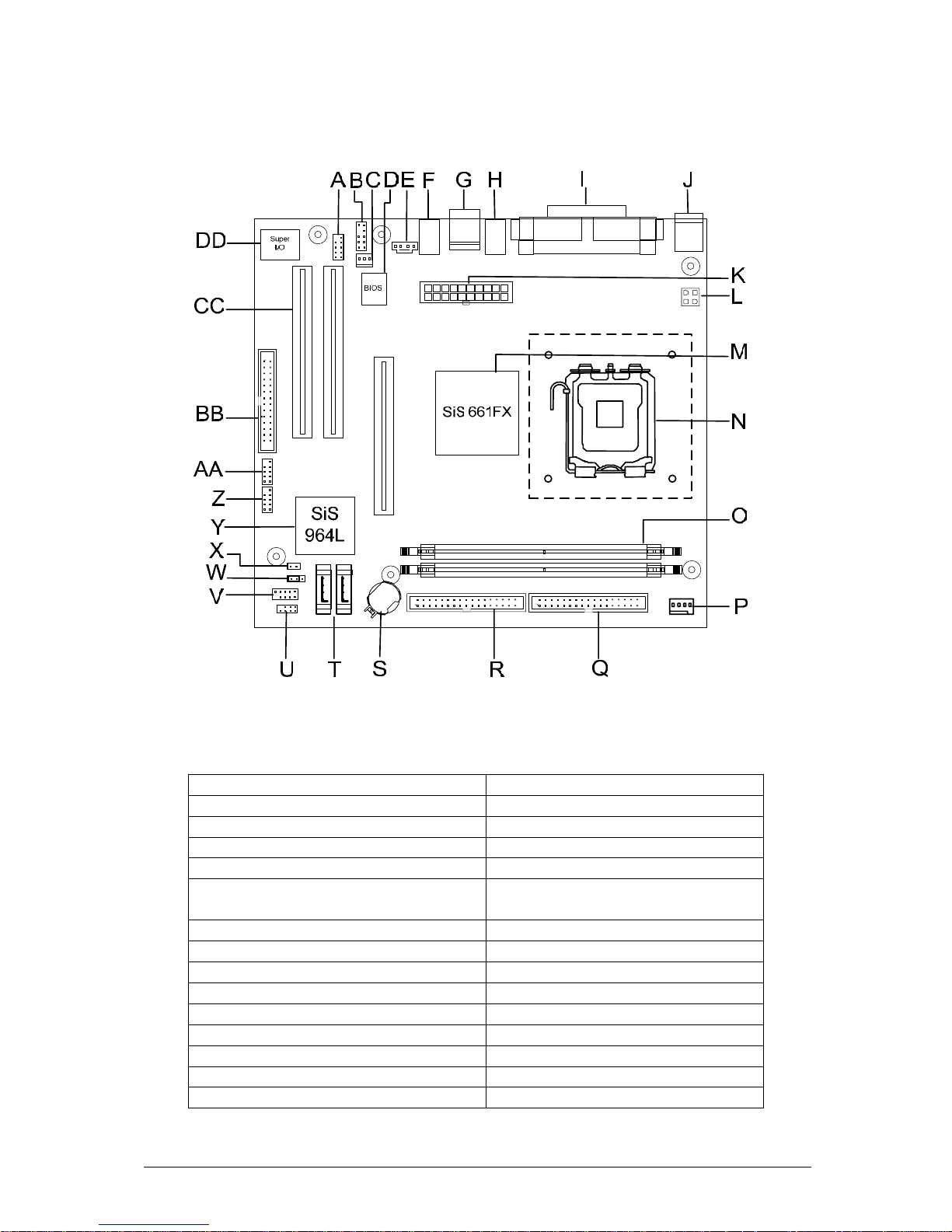
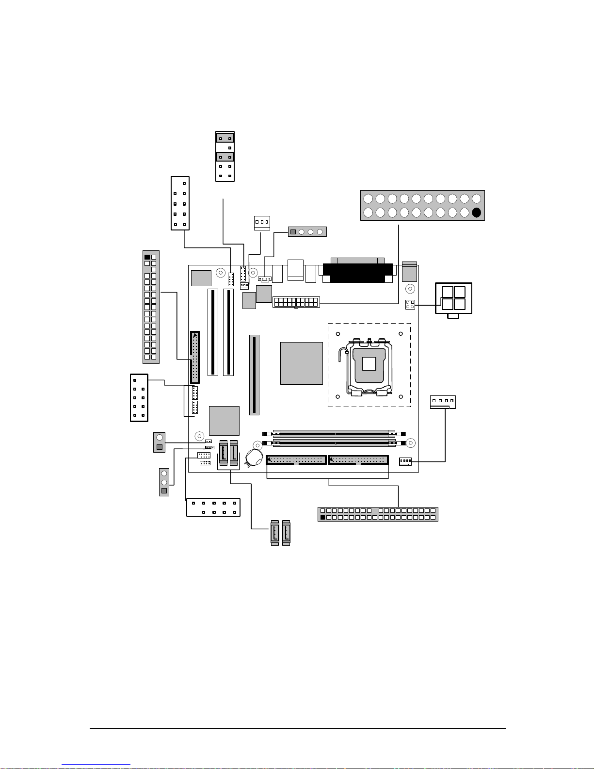
System Board Components
Figure 1: Motherboard Layout & Components
Table 2: Motherboard Connection
A: Serial header P: CPU Fan header
B: Audio header Q: IDE 2
C: Case Fan R: IDE 1
D: BIOS S: CMOS Battery
E: Audio CD in T: SATA 1 and 2
F: Rear Audio U: Power LED and speaker
header
G: LAN and USB V: Front Panel header
H: USB W: Clear CMOS jumper
I: VGA, Serial and Parallel X: Chassis intrusion header
J: PS/2 Keyboard and mouse Y: South Bridge
K: ATX 20 pin Z: USB header 1
L: ATX 4 pin AA: USB header 2
M: North Bridge BB: Floppy connector
N: 775 pin CPU socket CC: PCI slots
O: DIMM socket 1 and 2 DD: I/O chip

V1.0 VIG556M Motherboard Manual
15
Overview of System Board Components
A – Serial Header
Allows a serial device to be attached.
B – Audio Header
Allows a front audio panel to be connected. (Intel® Standard)
C – Case Fan Header
Allows a case fan to be connected to aid cooling.
D – BIOS
This controls the boot loader and all the hardware in the system.
E – Rear Audio
Allows a MIC, a Line-in and a Line-out to be connected.
F – Front Panel Audio
Allows a front facing audio panel to be fitted.
G – LAN and USB
Allows up to four USB devices to be connected and a network.
H – VGA, Serial and Parallel
Allows a VGA monitor, a serial device and a parallel device to be attached.
I – PS/2 Keyboard and mouse
Allows a PS/2 Keyboard and mouse to be attached.
K – 20 pin ATX power connector
This is the main power connector for the motherboard.
L – 4 pin ATX power connector
This provides power directly to the CPU and to the AGP port.
M – North Bridge
The SIS ® 611FX provides the processor interface with 800/533/400 MHz frequency,
support for Intel ® Hyper-Threading Technology, system memory interface at

V1.0 VIG556M Motherboard Manual
16
266MHz operation, and 1.5V AGP interface that supports AGP 2.0 specification
including 8x Fast Write protocol.
N – 775 pin CPU Socket
This is were the CPU is installed.
O – DIMM slots 1 and 2.
This allows up to 2GB of DDR RAM to be installed. Up to 1GB of RAM in each slot.
P – CPU Fan header
Allows a CPU fan to be connected
Q – Second IDE
This allows an additional 2 IDE device to be added to the motherboard. The port is
slotted to ensure correct installation.
R – Primary IDE
This allows up to 2 devices, such as CD/DVD drives and hard drives to be added
to the IDE channel. The port is slotted to ensure correct installation.
S – CMOS Battery
Supplies backup power to the CMOS. This keeps all the settings and information in
the BIOS.
T – SATA 0 and 1
This allows two SATA devices to be connected.
U – Power LED and speaker header.
This allows a three pin power LED and a speaker to be connected to the board.
V – Front Panel header
This allows the case cables to be connected, such as HDD LED, Reset switch and
power switch.
W – Clear CMOS jumper
Moving the jumper from the default position allows the CMOS to be cleared and
reset.

V1.0 VIG556M Motherboard Manual
17
X – Chassis intrusion
Allows a chassis intrusion switch to be added.
Y – South Bridge
The SIS® 964L integrated peripheral controller supports various I/O functions
including 2-channel ATA/133 bus master IDE controller, up to six USB 2.0 ports,
LPC Super I/O interface, AC’97 interface and PCI 2.2 interface.
Z – USB Header 1
This allows up to two USB devices to be connected though the use of a cable.
AA – USB Header 2
This allows an addition two USB devices to be connected though the use if a cable.
BB – Floppy Connector
Allows a floppy drive to be connected
CC – PCI slots
Allows two PCI devices to be connected to the board.
DD – I/O chip
This controls the Input and the Output on the motherboard
V1.0 VIG556M Motherboard Manual
18
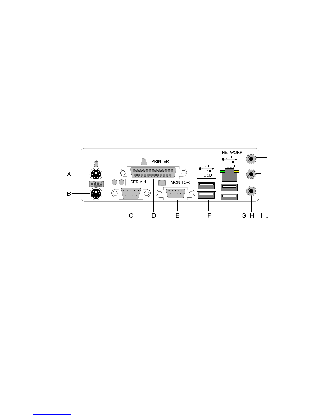
Back Panel Connectors
The motherboard external IO connectors are attached to a metallic I/O shield. This
shield serves several purposes:
• It protects the sensitive motherboard from any external EMC interference.
• It stops the computer from interfering with other electrical devices.
• It allows the motherboard to be easily upgraded in the future without having to
resort to buying a whole new case. Simply change the I/O shield to match the
motherboard.
The I/O shield provides external access to PS/2 keyboard and mouse connectors as
well as one serial port, one parallel port, four USB ports, one LAN Port and the audio
connectors.
Figure 2: Rear I/O Shield
NOTE: Power to the computer should be turned off before a keyboard or mouse is
connected or disconnected.
A/B – PS/2 Keyboard/Mouse Ports
The purple connector is for a PS/2 keyboard and the green connector is for a PS/2
mouse connector.
C – Serial Port
This 9-pin COM1 port is for a pointing device or other serial devices.
D – Parallel Port
This 25-pin port allows connection of a parallel device e.g. Printer, scanner etc
E –Video Graphics Adapter Port
This 15-pin port is for a VGA monitor or other VGA-compatible devices.

V1.0 VIG556M Motherboard Manual
19
F – USB 2.0 Ports
These 4-pin Universal Serial Bus (USB) ports are available for connecting USB 2.0
devices.
G – RJ-45 Port
This port allows connection to a Local Area Network (LAN) through a network hub.
H – Line-In Jack
This Line In (light blue) jack connects a tape player or other audio sources. In 6channel mode, the function of this jack becomes Bass/Center.
I – Line-Out Jack
This Line Out (lime) jack connects a headphone or a speaker. In 6-channel mode,
the function of this jack becomes Front Speaker Out.
J – Microphone Jack
This Mic (pink) jack connects a microphone. In 6-channel mode, the function of this
jack becomes Rear Speaker Out.
NOTE: The functions of the Line Out, Line In, and Microphone jacks change
when you select the 6-channel audio configuration.
Table 3: Audio 2, 4 or 6-channel configuration
Headphone/2Speaker
4-Speaker 6-Speaker
Light Blue
Line In Rear Speaker
Out
Rear Speaker
Out
Lime
Line Out Front Speaker
Out
Front Speaker
Out
Pink
Mic In Mic In Bass/Center
V1.0 VIG556M Motherboard Manual
20
Chapter 2: System Board Options
The VIG556M motherboard is capable of accepting Celeron® D, Pentium® 4 or
Pentium® D CPU’s. RAM can be upgraded to a maximum of 2GB using DDR266,
DDR333 or DDR400 SDRAM DIMMs Non ECC Unbuffered memory.
WARNING!
Unplug the system before carrying out the procedures described in this
chapter. Failure to disconnect power before you open the system can result
in personal injury or equipment damage. Hazardous voltage, current, and
energy levels are present in this product. Power switch terminals can have
hazardous Voltages present even when the power switch is off.
The procedures assume familiarity with the general terminology associated
with personal computers and with the safety practices and regulatory
compliance required for using and modifying electronic equipment.
Do not operate the system with the cover removed. Always replace the cover
before turning on the system.
As the colours of the wires in the mains lead of this computer may not correspond with the
coloured markings identifying the terminals in your plug precede as follows:
The wire which is coloured green-and-yellow must be connected to the terminal in the plug
which is marked by the letter E or by the safety Earth symbol Q or coloured green or
green-and-yellow.
The wire which is coloured blue must be connected to the terminal which is marked with
the letter N or coloured black.
The wire which is coloured brown must be connected to the terminal which is marked with
the letter L or coloured red.
CAUTION!
The Viglen VIG556M motherboard
and associated components are
sensitive electronic devices. A small
static shock from your body can
cause expensive damage to your
equipment.

V1.0 VIG556M Motherboard Manual
21
Make sure you are earthed and free of static charge before you open the computer
case. If you are unsure about upgrading your computer, return it to Viglen so a
qualified engineer can perform the upgrade.
STEPS TO TAKE TO PREVENT STATIC DISCHARGE:
1. The best way to prevent static discharge is to buy an anti-static strap from your
local electrical shop. While you are wearing the strap and it is earthed, static
charge will be harmlessly bled to ground.
2. Do not remove the component from its anti-static protective packaging until you
are about to install it.
3. Hold boards by the edges - try not to touch components / interface strips etc.
NOTE: We recommend that you return your computer to the service department for
upgrading. Any work carried out is fully guaranteed. Upgrades should only be carried
out by persons who are familiar with handling IC's, as incorrect installation will
invalidate the guarantee.

V1.0 VIG556M Motherboard Manual
22
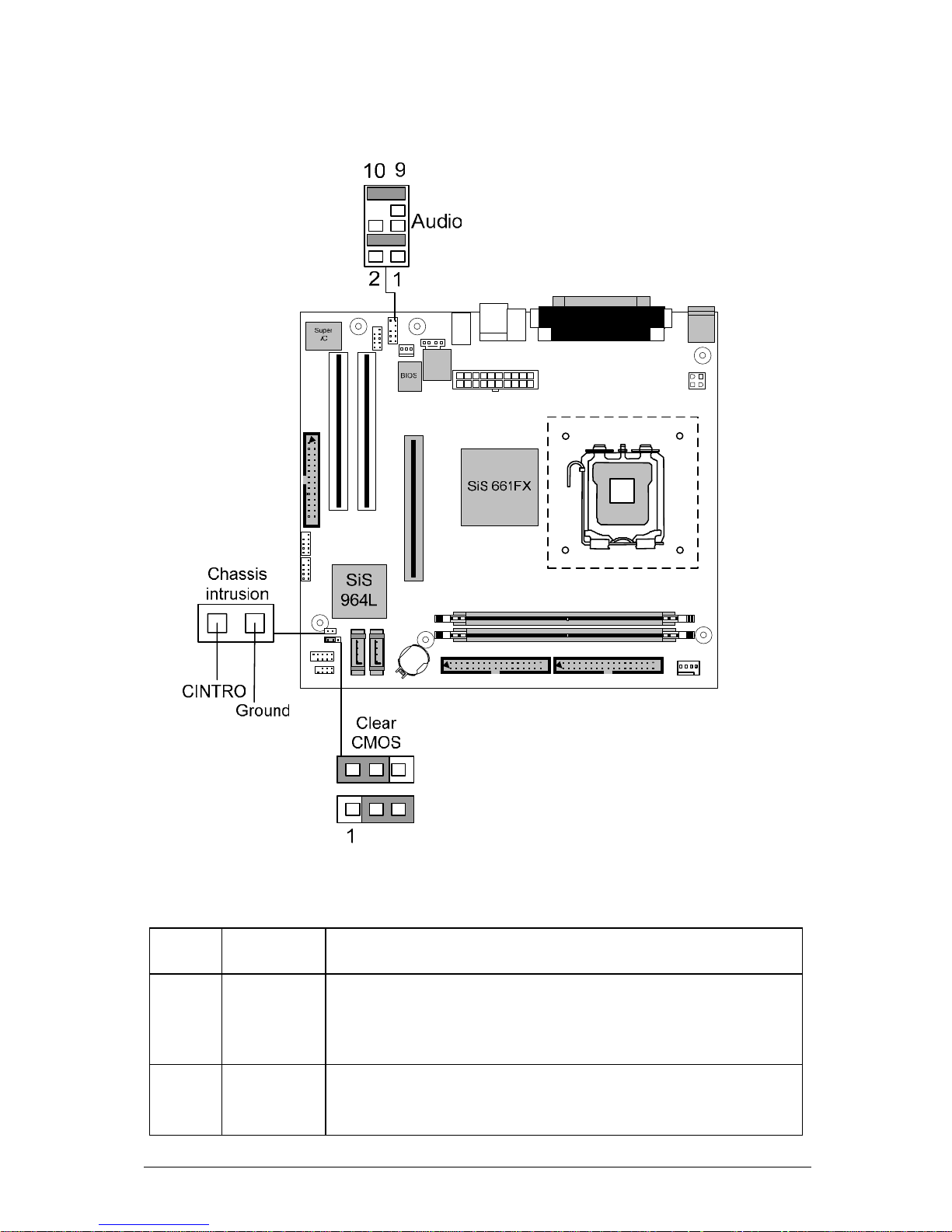
Overview of Jumper Settings
The VIG556M motherboard contains the latest technology to offer an almost
jumperless configuration. All Celeron® D, Pentium® 4 and Pentium® D CPUs are
automatically detected and the speed is automatically set from the information
provided by the CPU.
The only jumpers present on the motherboard are for clearing all the CMOS settings.
In the unlikely event of the CMOS becoming corrupted then jumper JP1 can be set to
clear the contents of the CMOS, and for write protecting the BIOS.
CAUTION!
Never remove jumpers using large pliers as this can damage the pins. The best way
to remove a jumper is to use a small pair of tweezers or fine needle-nosed pliers.
Never remove a jumper when the computer is switch on. Always switch the
computer off first.
V1.0 VIG556M Motherboard Manual
23
System Board Jumper Settings
Figure 3: System Board Jumper Settings
Table 4: Clear CMOS Jumper Settings
Functi
on
Jumper
(JP1)
Configuration
Save
CMOS
(Default
)
1-2 The BIOS uses current configuration information and
passwords for booting.
Clear 2-3 Turn off the system and unplug the power cord. Move the
jumper from pins 1-2 (default) to pins 2-3 for about 5~10
seconds. Then move the jumper back to pins 1-2.

V1.0 VIG556M Motherboard Manual
24
NOTE: Except when clearing the rtc ram, never remove the jumper on JP1 default
position. Removing the jumper will cause system boot failures.
Table 5: Front Panel Audio Jumper Settings
Function Jumper Configuration
Normal
5 – 6
and
9- 10
The audio line signals are routed back to
the line connector.
Table 5a: Front panel Audio Connector
Pin Signal name Pin Signal name
1 Audio Mic 2 Ground
3 Audio Mic Bias 4 VCC
5 Speaker Out
Right Channel
6 Speaker Out
Right Channel
Return
7 X 8 Key
9 Speaker Out Left
Channel
10 Speaker Out
Left Channel
Return
CAUTION!
Do not move the jumper with the power on. Always turn off the power and unplug
the power cord from the computer before changing the jumper.
NOTE: There is no jumper setting for configuring the processor speed or bus
frequency.
V1.0 VIG556M Motherboard Manual
25
Motherboard Connectors
There are connectors on the motherboard for FAN, IDE, Power supply, CD audio,
Floppy, IDE, & Front Panel Connectors. The location and/or details of these
connections are shown below.
Super
I/O
BIOS
SiS 661FX
SiS
964L
PSU
ATX
12V
Power Connector
11
20
10
Floppy
Drive
Connector
31
33
12
5
PCI IDE
Connector x
391
40202
1
FAN
Front
Chassis
Chassis
Intrusion
Configuration
Jumper
1
9
Serial ATA
Header
0& 1
1
FAN
Rear chassis
1
ATAPI
CDROM
Audio In
1
9
2
10
Front Panel
Audio
12
10
7
Front USB
Header
19
Front
Panel
COM 2
1
Figure 4: Motherboard Connectors

V1.0 VIG556M Motherboard Manual
26
Front Panel Connectors
The following are all connectors situated along the front edge of the motherboard.
They are often connected to buttons and LED’s situated on the front panel.
JFP1 JFP2
Figure 5: Front panel connectors
Hard Disk L.E.D. Connector
This goes to the Hard Disk L.E.D. on the front panel, which lights up when the IDE
Hard Disk is in use.
Reset switch connector
When these pins are shorted, it will cause the computer to perform a cold reboot.
Power L.E.D.
This attaches to the power L.E.D on the front panel, to display if the computer is
active or not. You can attach either a three pin LED or a 2 pin depending on what the
case is supplied with.
Power On/Off
When these pins are shorted it turns the computer on or off.

V1.0 VIG556M Motherboard Manual
27
Upgrading the CPU
CAUTION!
Allow time for the processor and heat sink to cool before touching either of them.
The Pentium® 4 & Pentium® D processor together with Level 2 cache chips are
housed in a protective package.
The design of the VIG556M computer makes it a simple job to replace or upgrade
the processor. To do so please refer to figure 6 and follow the instructions below:
1. The CPU has a plastic cap on it to protect the contact from damage. Before
you have installed the CPU, always cover it to protect the socket pin. Remove
the cap from lever hinge side. The pins of socket reveal. Lift the load lever up
and open the load plate.
2. The CPU has a cover on the bottom to prevent contact damage.
Rotate it to make the pin 1 indicator (yellow triangle) in the left-bottom
corner. The availability of it depends on the CPU packing.
3. Use 2 hands to remove the cover on the bottom of the CPU (if any). Please
note not to touch the underside of it.
4. Align the pin 1 indicators (the triangles on the CPU).
5. Using your forefinger and thumb place CPU in socket. Being careful not to
move the CPU whilst in the socket.
6. Lay the load plate on top of the CPU and press down the load lever until the
lever is locked in place.

V1.0 VIG556M Motherboard Manual
28
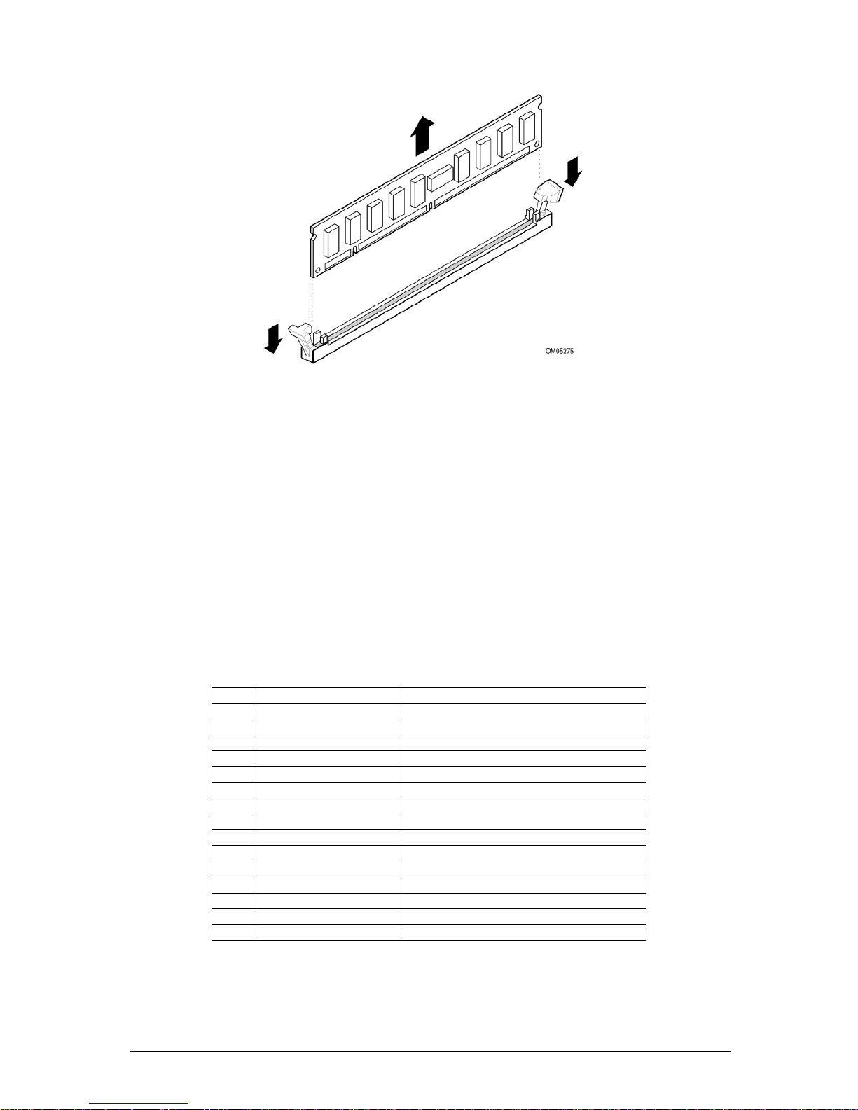
Installing & Removing Memory Modules
Installing Memory
You can install from 64MB to 2GB of memory in the motherboard DIMM sockets.
The motherboard has two DIMM sockets. The motherboard supports the following
memory features:
• 184-pin DIMMs with gold-plated contacts.
• Non-ECC (64-bit) memory.
• 64MB, 128MB, 256MB, 512MB and 1GB modules.
NOTE: DDR SDRAM must meet the Version 1.0 June 2000 JEDEC Solid State
Technology Association specifications for DDR266 SDRAM.
To install DIMMs, follow these steps:
1. Observe the precautions in “Before You Begin”. Turn off the computer and all
Peripheral devices.
2. Remove the computer cover and locate the DIMM sockets.
3. Holding the DIMM by the edges, remove it from its antistatic package.
4. Make sure the clips at either end of the socket are pushed away from the socket.
5. Position the DIMM above the socket. Align the two small notches in the bottom
edge of the DIMM with the keys in the socket. Insert the bottom edge of the
DIMM into the socket.
6. When the DIMM is seated, push down on the top edge of the DIMM until the
retaining clips at the ends of the socket snap into place. Make sure the clips are
firmly in place.
7. Replace the computer cover.
Removing Memory
To remove a DIMM, follow these steps:
1. Observe the precautions in "Before You Begin”.
2. Turn off all peripheral devices connected to the computer. Turn off the computer.
3. Remove the computer cover.
4. Gently spread the retaining clips at each end of the socket. The DIMM pops out
of the socket.
Hold the DIMM by the edges, lift it away from the socket, and store
it in an antistatic package.
5. Reinstall and reconnect any parts you removed or disconnected to reach the
DIMM sockets.
V1.0 VIG556M Motherboard Manual
29
Figure 6: Removing Memory Modules
Expansion Slots
The motherboard has two PCI slots and one Accelerated Graphics Port (AGP) slot.
To install and configure an expansion card:
1. Install an expansion card following the instructions that came with the chassis.
2. Turn on the system and change the necessary BIOS settings, if any. See Chapter
4, System BIOS.
3. Assign an IRQ to the card. Refer to the tables below.
4. Install the drivers and/or software applications for the expansion card according
to the card documentation.
Table 6: Standard IRQ Assignment
IRQ Priority Standard Function
0 1 System Timer
1 2 Keyboard Controller
2 N/A Programmable Interrupt
4* 12 Communication Port (COM1)
5* 13 IRQ Holder for PCI steering
6 14 Floppy Disk Controller
7* 15 Printer Port (LPT1)
8 3 System CMOS/Real Time Clock
9* 4 IRQ Holder for PCI steering
10* 5 Advanced AC’97 CODEC
11* 6 Standard PCI Graphics Adapter (VGA)
12* 7 PS/2 Compatible Mouse Port
13 8 Numeric Data Processor
14* 9 Primary IDE Channel
15* 10 Secondary IDE Channel
* These IRQs are usually available for ISA or PCI devices

V1.0 VIG556M Motherboard Manual
30
PCI Slots
There are two 32-bit PCI slots on this motherboard. The slots support PCI cards
such as a LAN card, SCSI card, USB card, and other cards that comply with PCI
specifications.
Figure 7: Installing a PCI card
AGP Slot
This motherboard has an Accelerated Graphics Port (AGP) slot that supports AGP
8X (3.3V/1.5V) cards.
NOTE: The notches on the card golden fingers to ensure that they fit the AGP slot on
your motherboard.
Figure 8: Install an AGP card

V1.0 VIG556M Motherboard Manual
31
Replacing the Clock/CMOS RAM Battery
A lithium battery is installed in a socket on the system board.
The battery has an estimated life expectancy of seven years. When the battery
starts to weaken, it loses voltage; when the voltage drops below a certain level, the
system settings stored in CMOS RAM (for example, the date and time) may be
wrong.
If the battery fails, you will need to replace it with a CR2032 battery or an equivalent.
As long as local ordinance permits, you may dispose of individual batteries as
normal rubbish. Do not expose batteries to excessive heat or any naked flame.
Keep all batteries away from children.
CAUTION!
Danger of explosion if the battery is incorrectly replaced. Replace only with the
same or equivalent type recommended by Viglen. Discard used batteries according
to manufacturer’s instructions.
The battery is listed as board component ‘S’ on the diagram on Figure 1.
To replace the battery, carry out the following:
1. Observe the precautions in “Before You Begin.”
2. Turn off all peripheral devices connected to the system.
3. Turn off the system.
4. Remove any components that are blocking access to the battery.
5. Figure 1 shows the battery location. Gently pry the battery free from its socket,
taking care to note the "+" and "-" orientation of the battery (Figure 10).
6. Install the new battery in the socket.
Figure 9: Removing the Battery
1
+
+
2

V1.0 VIG556M Motherboard Manual
32
Chapter 3: Solving Problems
The first part of this chapter helps you identify and solve problems that might occur
when the system is in use. The second part lists error code messages that might be
displayed.
Please remember that if you cannot solve the problem by yourself then you should
contact your suppliers Technical Support for further assistance.
Viglen Technical Support can be reached in the following ways:
Telephone: 08705 922 922
Fax: 01727 201 888
Email: techsupport@viglen.co.uk
You can also look for support information on our web site:
http://www.viglen.co.uk
Device drivers and various useful utilities can be downloaded from our ftp site:
ftp://ftp.viglen.co.uk
Resetting the System
Before checking your system for hardware problems, it is always a good idea to try
resetting your computer and see if a re-boot can solve the problem. Most software
related problems can be solved simply by re-booting your PC.
Table 7: Resetting the System
To do the following Press
Soft boot: Clear the system
memory and reload the operating
system (also called warm reset).
<Ctrl + Alt + Del>
Cold boot: Clear the system
memory, halt power to all
peripherals, restart POST, and
reload the operating system.
Power off/on or reset button
(at front of the system)

V1.0 VIG556M Motherboard Manual
33
Troubleshooting Procedures
This section provides a step-by-step troubleshooting procedure to identify a problem
and locate its source.
CAUTION!
1. Turn off the system and any peripheral devices before you disconnect any
peripheral cables from the system. Otherwise, you can permanently damage the
system or the peripheral devices.
2. Make sure the system is plugged into a properly grounded power outlet.
3. Make sure your keyboard and video display are correctly connected to the
system. Turn on the video display, and turn up its brightness and contrast
controls to at least two-thirds of the maximum (refer to the documentation supplied
with the video display).
4. If the operating system normally loads from the hard disk drive, make sure there is
no diskette in the diskette drive. If the operating system normally loads from a
diskette, insert the operating system diskette into the drive.
5. Turn on the system. If the power indicator does not light, but the system seems
to be operating normally, the indicator is probably defective. Monitor the power-on
self test (POST) execution. Each time you turn on the system, the POST checks
the system board, memory, keyboard, and certain peripheral devices.
NOTE: If the POST does not detect any errors, the system beeps once and boots
up.
Errors that do not prevent the boot process (non-fatal errors) display a message that
looks similar to the following:
Error Message Line 1
Error Message Line 2
Press <F2> for Set-up, <F1> to Boot
You can note the error and press <F1> to resume the boot- up process, or
<F2> to enter Set-up.
Errors that prevent the boot process from continuing (fatal errors), are communicated
by a series of audible beeps. If this type of error occurs, refer to the error codes and
messages listed at the end of this chapter.
6. Confirm that the operating system has loaded.

V1.0 VIG556M Motherboard Manual
34
Problems Operating Add-in Boards
Problems related to add-in boards are usually related to improper board installation
or interrupt and address conflicts. Go through the checklist below to see if you can
correct the problem. If the problem persists after you have checked and corrected all
of these items, contact the board vendor's customer service representative.
Did you install the add-in board according to the manufacturer’s instructions?
Check the documentation that came with the board. Are all cables installed properly?
The following items are suggestions for troubleshooting problems related to PCI/ISA
legacy (non-Plug and Play) add-in boards.
• If the PCI/ISA board uses an interrupt, run Set-up and set the interrupt that is
being used by the PCI/ISA board to Used by PCI/ISA Card. Please refer to the
BIOS manual for details of how to do this.
• If the PCI/ISA legacy board uses memory space between 80000H - 9FFFFH, run
Set-up and set conventional memory to 256 K.
• If the PCI/ISA legacy board uses shared memory between C8000H - DFFFH, run
Set-up and enable shared memory for the appropriate memory space.

V1.0 VIG556M Motherboard Manual
35
Problems & Suggestions
Table 8: Problems and Suggestions
What happens What to do
Application
software
problems
Try resetting the system.
Make sure all cables are installed correctly.
Verify that the system board jumpers are set properly.
Verify that your system hardware configuration is set
correctly. In Setup, check the values against the system
settings you recorded previously. If an error is evident
(wrong type of drive specified, for example), make the
change in Setup and reboot the system. Record your
change.
Make sure the software is properly configured for the
system. Refer to the software documentation for
information.
Try a different copy of the software to see if the problem is
with the copy you are using.
If other software runs correctly on the system, contact the
vendor of the software that fails.
If you check all of the above with no success, try clearing
CMOS RAM and reconfiguring the system. Make sure
you have your list of system settings available to re-enter,
because clearing CMOS RAM sets the options to their
default values.
Characters onscreen are
distorted or
incorrect
Make sure the brightness and contrast controls are
properly adjusted on the monitor.
Make sure the video signal cable and power cables are
properly installed.
Make sure your monitor is compatible with the video
mode you have selected.
Characters do not
appear on screen
Make sure the video display is plugged in and turned on.
Check that the brightness and contrast controls are
properly adjusted.
Check that the video signal cable is properly installed.
Make sure a video board is installed, enabled, and the
jumpers are positioned correctly.
Reboot the system.

V1.0 VIG556M Motherboard Manual
36
Table 8: Problems and Suggestions (Continued)
What happens What to do
CMOS RAM
settings are wrong
If system settings stored in CMOS RAM change for no
apparent reason (for example, the time of day develops
an error), the backup battery may no longer have enough
power to maintain the settings. Replace the battery
(Chapter 2).
Diskette drive light
does not go on
when drive is in
use or is tested by
POST
Make sure the power and signal cables for the drive are
properly installed.
Check that the drive is properly configured and enabled in
Setup.
Hard drive light does
not go on when drive
is in use or is tested
by POST
Make sure the power and signal cables for the drive are properly
installed.
Make sure the front panel connector is securely attached to the
system board headers.
Check that the drive is properly configured and enabled in Setup.
Check the drive manufacturer's manual for proper configuration for
remote hard disk drive activity.
Power-on light does
not go on
If the system is operating normally, check the connector between the
system board and the front panel. If OK, the light may be defective.
Prompt doesn't
appear after system
boots
It’s probably switched off.
A serious fault may have occurred consult your dealer service
department / Technical Support.
Setup, can't enter
If you can't enter Setup to make changes, check the switch that
disables entry into Setup (Chapter 2). If the switch is set to allow
entry into Setup, you might need to clear CMOS RAM to the default
values and reconfigure the system in Setup.
System halts before
completing POST
This indicates a fatal system error that requires immediate service
attention. Note the screen display and write down any beep code
emitted. Provide this information to your dealer service department /
Technical Support.

V1.0 VIG556M Motherboard Manual
37
Chapter 4: System BIOS
What is the BIOS?
The BIOS (Basic Input Output System) is an important piece of software which is
stored in a ROM (Read Only Memory) chip inside the computer. It consists of the
basic instructions for controlling the disk drives, hard disk, keyboard and
serial/parallel ports. The BIOS also keeps a list of the specifications of the computer
in battery-backed RAM (also known as the CMOS RAM) and provides a special
Setup program to change this information.
The BIOS in your Viglen computer is guaranteed to be fully compatible with the IBM
BIOS. It has been written by Phoenix Award BIOS, an industrial leader in the field of
BIOS software.
The Power-On sequence
When the computer is first switched on, certain instructions in the BIOS are executed
to test various parts of the machine. This is known as the POST (Power-On Self
Test) routine. When you switch the computer on (or when you press the Reset
button or press <Ctrl> + <Alt>+ <Delete> keys, which has the same effect), you can
see on the monitor that it counts through the memory, testing it. The floppy disk
drives are then accessed and tested, and the various interfaces are checked. If there
are any errors, a message is displayed on the screen.
Having passed all the tests, and if you have activated the password facility, the BIOS
then asks you to enter the boot password to continue. The following section
describes how to do this. The BIOS then loads the operating system, either - MS
DOS, Windows 98SE, OS/2 or NetWare, etc. - from the hard disk (or floppy disk if
one is inserted in Drive A: The computer is then ready for use.

V1.0 VIG556M Motherboard Manual
38
Phoenix Award BIOS
Introduction
The motherboard uses a Phoenix BIOS, which is stored in flash memory and can be
upgraded using a disk-based program. In addition to the BIOS, the flash memory
contains the Setup program, Power-On Self Test (POST), Advanced Power
Management (APM), the PCI auto-configuration utility, and is Windows 95-ready
Plug and Play. This motherboard supports system BIOS shadowing, allowing the
BIOS to execute from 64-bit onboard write-protected DRAM.
The BIOS displays a message during POST identifying the type of BIOS and the
revision code.
BIOS Upgrades
A new version of the BIOS can be upgraded from a diskette using the AFUDOS.EXE
utility that is available from the Viglen FTP site. This utility does BIOS upgrades as
follows:
• Updates the flash BIOS from a file on a disk.
• Updates the language section of the BIOS.
• Makes sure that the upgrade BIOS matches the target system to prevent
accidentally installing a BIOS for a different type of system.
BIOS upgrades and the AWFL855A.EXE utility may be available online at
www.viglen.co.uk or by request.
NOTE: Please review the instructions distributed with the upgrade utility before
attempting a BIOS upgrade.
Using AWDFLASH to update the BIOS
The BIOS can be updated using the AWFL855A.EXE utility in DOS environment.
• Copy the AWFL855A.EXE utility to the bootable floppy disk that contains the
BIOS file.
• Boot the system from the floppy disk.
• At the DOS prompt, type the command line:
Awfl855a filename.bin
Where “filename.bin” means the latest (or original) BIOS file that you copied to the
bootable floppy disk.
The whole process is automated and needs no input from the user.
DO NOT shutdown or reset the system while updating the BIOS! Doing so may
cause system boot failure!

V1.0 VIG556M Motherboard Manual
39
When the BIOS update process is complete, the utility reboots the system.
Once the system has been restarted it will hold on the Pre-BIOS screen. At this
stage the following need to be completed before starting windows.
1. The system will halt on pre-BIOS, at this point you need to shut the machine
down.
2. Reboot the computer.
3. System will holt on the pre-BIOS screen and display an error message
(CMOS checksum error – Defaults loaded)
4. Enter the BIOS setup by pressing DEL
5. Once in the setup load the optimized settings by selecting ‘Load Optimized
Defaults’
6. Exit the setup by selecting ‘Save & Exit setup’.
7. Now boot in to windows.
When you reboot the system it will hold on the Pre-BIOS screen. At this stage there
will be an error message shown and details of the current BIOS. Check the BIOS
version. The BIOS version is made up of the BIOS file name, version, build and time
of flash. E.g.
W7103SMS V1.0 121404 14:27:50
The V number is the version, in this case Version 1.0.
This requires the user to choose one of two options. Either F1 to continue with the
default BIOS settings loaded or DEL to enter the BIOS setup.
Enter the BIOS setup and select ‘load optimized default’. Then select ‘Save & Exit
setup’.

V1.0 VIG556M Motherboard Manual
40
Configuring the Motherboard using BIOS Setup
Before You Begin
CAUTION!
• Always follow the steps in each procedure in the correct order.
• Set up a log to record information about your computer, such as model, serial
numbers, installed options, and configuration information.
• Use an anti-static wrist strap and a conductive foam pad when working on the
motherboard.
WARNINGS
The procedures in this chapter assume familiarity with the general terminology
associated with personal computers and with the safety practices and regulatory
compliance required for using and modifying electronic equipment.
Disconnect the computer from its power source and from any telecommunications
links, networks, or modems before performing any of the procedures described in
this chapter. Failure to disconnect power, telecommunications links, networks, or
modems before you open the computer or perform any procedures can result in
personal injury or equipment damage. Some circuitry on the motherboard may
continue to operate even though the front panel power button is off.
CAUTION!
Electrostatic discharge (ESD) can damage components. Perform the procedures
described in this chapter only at an ESD workstation. If such a station is not
available, you can provide some ESD protection by wearing an anti-static wrist strap
and attaching it to a metal part of the computer chassis.

V1.0 VIG556M Motherboard Manual
41
BIOS Setup Program
This motherboard supports a programmable firmware hub (FWH) that you can
update using the provided utility described in section “2.1 Managing and updating
your BIOS.”
Use the BIOS Setup program when you are installing a motherboard, reconfiguring
your system, or prompted to “Run Setup”. This section explains how to configure
your system using this utility.
Even if you are not prompted to use the Setup program, you may want to change the
configuration of your computer in the future. For example, you may want to enable
the security password feature or change the power management settings. This
requires you to reconfigure your system using the BIOS Setup program so that the
computer can recognise these changes and record them in the CMOS RAM of the
firmware hub.
The firmware hub on the motherboard stores the Setup utility. When you start up the
computer, the system provides you with the opportunity to run this program. Press
<Delete> during the Power-On Self Test (POST) to enter the Setup utility. Otherwise,
POST continues with its test routines.
If you wish to enter Setup after POST, restart the system by pressing <Ctrl> + <Alt>
+ <Delete>, or by pressing the reset button on the system chassis. You can also
restart by turning the system off and then back on. Do this last option only if the first
two failed.
The Setup program is designed to make it as easy to use as possible. It is a menu
driven program, which means you can scroll through the various sub-menus and
make your selections from the available options using the navigation keys.
NOTE: If the system becomes unstable after changing any BIOS settings, load the
default settings to ensure system stability. Select the Load Default Settings item
under the Exit Menu.

V1.0 VIG556M Motherboard Manual
42
Main Menu Items
The Main menu is the first screen you are presented with on entering the BIOS
setup.
Figure 10: Main Manu
Sub Menu Items: An item with a sub-menu on any menu screen is distinguished
by a solid triangle before the item. To display the sub-menu, select the item and
press Enter.
Configuration Fields: These fields show the values for the menu items. If an
item is user-configurable, you may change the value of the field opposite the item.
You cannot select an item that is not user-configurable.
A configurable field is enclosed in brackets, and is highlighted when selected. To
change the value of a field, select it then press Enter to display a list of options.
Pop Up Window:
Select a menu item then press Enter to display a pop-up
window with the configuration options for that item.
Scroll Bar : A scroll bar appears on the right side of a menu screen when there
are items that do not fit on the screen. Press left/right or Up/Down arrow keys or
PageUp/PageDown keys to display the other items on the screen.
General Help: To view general help press F1. This displays help information
on the particular option you are in.

V1.0 VIG556M Motherboard Manual
43
Main BIOS Menu Screen
Figure 11: BIOS Menu Screen
Standard CMOS features: For changing the basic system configuration
Advanced BIOS features: For accessing advanced system settings
Advanced Chipset Features: For accessing Advanced chipset settings
Integrated Peripherals: For changing PCI, AGP and USB settings
Power Management Setup: For accessing advanced power management (APM)
configuration
PnP/PCI Configurations: For changing IRQ settings
PC Health Status: Displays information regarding CPU temp and fan speed
Frequency/Voltage Control: For changing the CPU frequency and displaying
current frequency information
Load Optimized Defaults: loads BOIS default values
BIOS setting password: option that allows a password to be set to access and
change BIOS settings.

V1.0 VIG556M Motherboard Manual
44
Save & Exit Setup: this option will save any changes made that have been made
whilst using the BIOS CMOS setup utility and exit out of the BIOS CMOS setup
utility.
Exit Without Saving: this option will not save any changes made that have been
made whilst using the BIOS CMOS setup utility and exit out of the BIOS CMOS
setup utility.

V1.0 VIG556M Motherboard Manual
45
Standard CMOS Features
When you enter the BIOS Setup program, the Main menu screen appears giving you
an overview of the basic system information.
Phoenix – AwardBIOS CMOS Setup Utility
Standard CMOS Features
Date (mm:dd:yy) Mon, Dec 1 2003
Time (HH:MM:SS) 11 : 20 : 43
► IDE Primary Master None
► IDE Primary Slave None
► IDE Sceondry Master CDU5211
► IDE Secondry Slave None
Floppy Drive A 1.44MB
Halt On All Errors
Menu Level ►
Change the day, month,
year and century
↑↓→←:Move Enter:Select +/-/PU/PD:Value F10:Save ESC:Exit F1:General Help
F5:Previous Values F7: Optimized Defualts
Item Help
Figure 12: Standard CMOS features
System Date: This item allows you to set the system date [mm:dd:yyyy].
System Time: This item allows you to set the system time [hh:mm:ss]
IDE Primary/Secondary Master/Slave: This shows what devices are running of
which IDE channel.
Floppy Drive A [1.44M, 3.5 in.]: Sets the type of floppy drive installed. Configuration
options: [Disabled] [360K, 5.25 in.] [1.2M, 5.25 in.] [720K, 3.5 in.] [1.44M, 3.5 in.] [2.88M,
3.5 in.]
Halt On: This item determines whether the system stops if an error is detected
during system boot-up. Options that are given are:
[All Errors]
[No Errors]
[All, But keyboard]
[All, But Diskette]
[All, But Disk/Key]

V1.0 VIG556M Motherboard Manual
46
IDE Primary/Secondary Master/Slave
Figure 13: IDE Device Sub-Menu
LBA/Large Mode: This indicates the mode of the hard drive. Leave on auto if mode
is not known.
DMA Mode: Allows the hard drive direct access to the memory.
Hard Drive S.M.A.R.T: If the hard drive used supports S.M.A.R.T (Self-Monitoring,
Analysis and Reporting Technology)
then this allows all the functions to be used.
Size: This indicates the capacity of the hard drive.

V1.0 VIG556M Motherboard Manual
47
Advanced BIOS features
The Advanced menu items allow you to change the settings for the CPU and
other system devices.
CAUTION!
Take caution when changing the settings of the Advanced menu items. Incorrect
field values may cause the system to malfunction.
Figure 14: Advanced BIOS features Sub-Menu
Quick Booting: This speeds up the boot time of the system by not running a full
memory test. If disabled, the boot time varies according to the amount of memory
installed.
Boot to OS/2: This tells the BIOS whether OS/2 is being used and adjusts settings
accordingly.
Hyper-Threading Function: This allows full functionality of hyper-threading CPU’s
to be used.
MPS Table version: The version of the MPS table being used.
Set Limit CPUID MaxVal to 3: Sets the CPUID limit to 3
V1.0 VIG556M Motherboard Manual
48
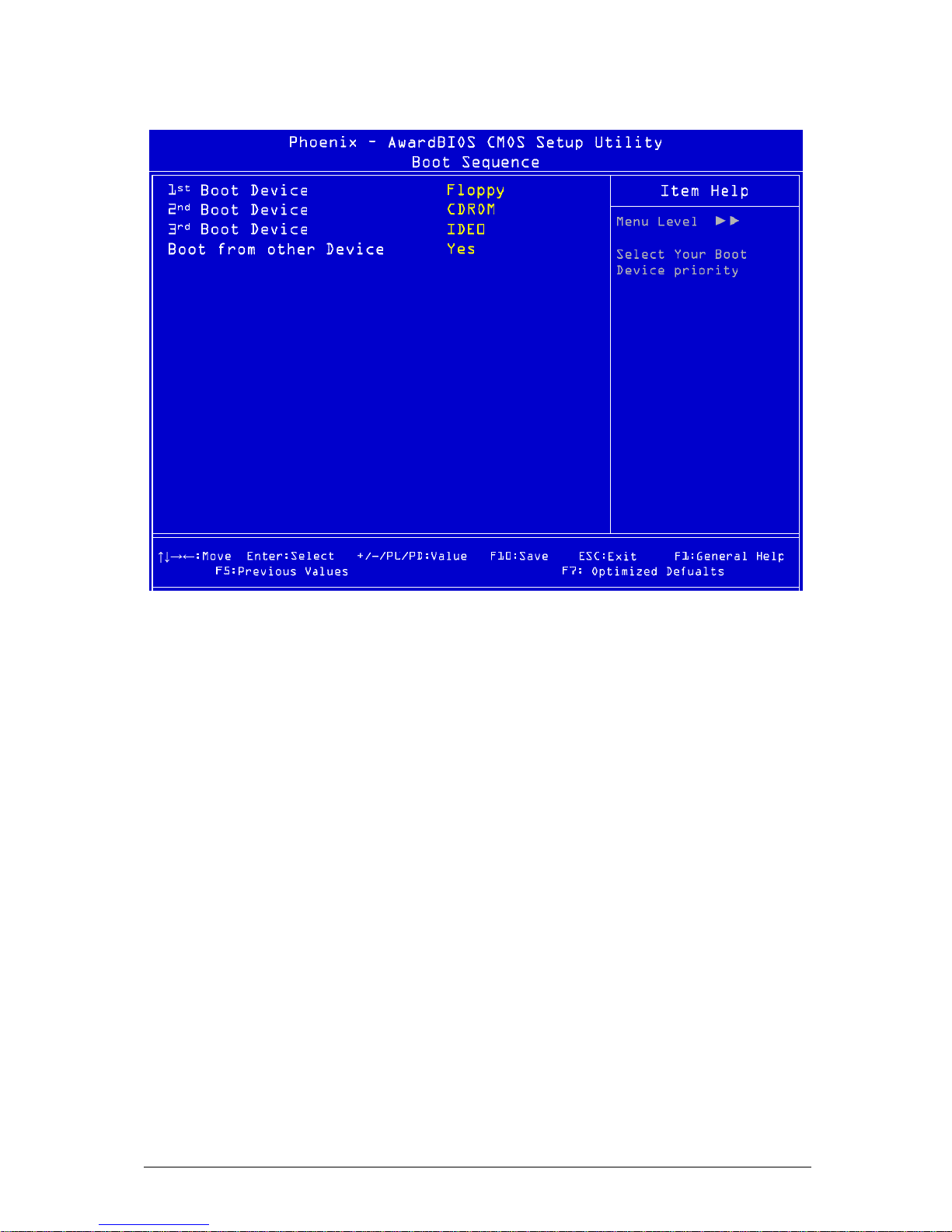
Boot Sequence
Figuer 15. Boot sequence Sub-menu
1st Boot Device: The 1st device the system tries to boot from
2nd Boot Device: The 2nd device the system tries to boot from
3rd Boot Device: The 3rd device the system tries to boot from
Boot from other Device: Allows another device to be booted from such as a USB
device.

V1.0 VIG556M Motherboard Manual
49
Advanced Chipset Features
Figure 16: Advanced Chipset Features
DRAM Clock/Timing Control: Allow control over the timing of the DRAM
AGP & P2P Bridge Control: Allows control over the AGP Bridge
OnChip AGP Control: Controls the AGP

V1.0 VIG556M Motherboard Manual
50
DRAM Timing Control
Phoenix – AwardBIOS CMOS Setup Utility
DRAM Clock/Timing Control
Performance Mode Enabled
DRAM Timing Control By SPD
x DRAM CAS Latency 2.5T
x RAS Active Time(tRAS) 6T
x RAS Precharge Time(tRP) 3T
x RAS to CAS Delay(tRCD) 3T
MA 1T/2T Select Auto
Menu Level ►►
↑↓→←:Move Enter:Select +/-/PU/PD:Value F10:Save ESC:Exit F1:General Help
F5:Previous Values F7: Optimized Defualts
Item Help
Figure 17: DRAM Timing Control
Memory Timing
Allows the used to select the CAS latency time in HCLKs of 2, 2.5 or 3. The value is
set the factory depending on the DRAM installed. DO NOT change the values in this
field unless you have changed the DRAM or CPU.

V1.0 VIG556M Motherboard Manual
51
AGP & P2P Bridge Control
Phoenix – AwardBIOS CMOS Setup Utility
AGP & P2P Bridge Control
AGP Aperture Size 128MB
AGP Fast Write Support Disabled
AGP Data Rate Auto
Menu Level ►►
↑↓→←:Move Enter:Select +/-/PU/PD:Value F10:Save ESC:Exit F1:General Help
F5:Previous Values F7: Optimized Defualts
Item Help
Figure 18: AGP & P2P Bridge Control
AGP Aperture Size: This controls how much system RAM is allocated to the AGP
for video purposes.
AGP Fast Write Support: Enables and disables AGP fast write support.
AGP Data Rate: This allows the user to control the AGP card data transfer rate.

V1.0 VIG556M Motherboard Manual
52
OnChip AGP Control
Figure 19: OnChip AGP Control
VGA Share Memory Size: This shows the amount of memory shared from the main
memory for use with the VGA. In the case above the memory being used for the
VGA is 32MB; this also means that 32MB will be de-allocated from the main
memory.
Graphics Engine Clock: This displays the speed at which the Graphics clock is
running.

V1.0 VIG556M Motherboard Manual
53
Integrated Peripherals
Figure 20: Integrated Peripherals
Integrated Peripherals: Integrated peripherals sub menus

V1.0 VIG556M Motherboard Manual
54
SIS OnChip PCI Device
Phoenix – AwardBIOS CMOS Setup Utility
SIS OnChip PCI Device
SIS USB Controller Enabled
USB 2.0 Supports Enabled
USB Keyboard Support Enabled
USB Mouse Support Enabled
SIS AC97 Audio Enabled
SIS Serial ATA Controller Enabled
SIS 10/100 ETHERNET Enabled
Onboard LAN Option ROM Enabled
Menu Level ►►
↑↓→←:Move Enter:Select +/-/PU/PD:Value F10:Save ESC:Exit F1:General Help
F5:Previous Values F7: Optimized Defualts
Item Help
Figure 21: SIS OnChip PCI Device
SIS USB Controller: This enables the USB controller. Leave as the default ‘Enable’
if you wish to add a USB device to your computer.
USB 2.0 Supports: Enables USB 2.0 support on your computer.
USB Keyboard Support: This allows a USB keyboard to be used in a DOS
environment by selecting [BIOS] or in the OS by selecting [OS].
USB Mouse Support: This allows a USB mouse to be used in a DOS environment
by selecting [BIOS] or in the OS by selecting [OS].
SIS AC97Audio: This allows you to control the onboard AC97 audio. Disable this
item if you are going to install a PCI audio add-on card.
SIS Serial ATA Controller: Enables support for SATA devices.
SIS 10/100 EHTERNET: Enables the on-board LAN
On-board LAN option ROM: Enables LAN boot ROM support

V1.0 VIG556M Motherboard Manual
55
IDE Device Configuration
Phoenix – AwardBIOS CMOS Setup Utility
IDE Device Configuration
Internal PCI/IDE Both
IDE DMA transfer Access Enabled
Menu Level ►►
↑↓→←:Move Enter:Select +/-/PU/PD:Value F10:Save ESC:Exit F1:General Help
F5:Previous Values F7: Optimized Defualts
Item Help
Figure 22: OnChip IDE Device
Internal PCI/IDE: Used to enable or disable the internal PCI IDE channel.
IDE DMA transfer Access: Enables DMA access for the IDE device

V1.0 VIG556M Motherboard Manual
56
I/O Device Configuration
Figure 23: OnChip PCI Device
Onboard FDC Controller: Enables the Floppy Disk Controller.
Onboard Serial Port ½: Enables the serial ports on the motherboard
UART Mode Select: Sets the mode for the serial port.
Onboard Parallel Port: Sets the IRQ for the Parallel port
Parallel Port Mode: Sets the mode for the Parallel port.
ECP Mode Use DMA: Sets the DMA used by the Parallel port.

V1.0 VIG556M Motherboard Manual
57
Power Management Setup
Figure 24: Onboard SuperIO device
ACPI function: Enables the ACPI features of the CPU
ACPI Standby State: Sets the suspend mode of the system
Suspend Time Out (Minute): Time before the system goings into suspend.
Hot Key Function As: This allows a hot key to be set to send the system into
suspend
Power button function: This dictates how the power button operates.
Restore on AC power lost: This dictates how the system reacts to total power loss.
Wake up Event Setup: Configures the events that may wake the system.

V1.0 VIG556M Motherboard Manual
58
Wake up Event Setup
Phoenix – AwardBIOS CMOS Setup Utility
Wake up Event Setup
Resume From S3 By USB Device Enabled
Resume By PS/2 Keyboard Any Key
Resume By PS/2 Mouse Move & Click
Resume By PCI Device(PME#) Enabled
MACPME Power Up Control Disabled
Resume By RTC Alarm Disabled
x Month Alarm NA
x Day of Month Alarm 0
x Time (hh:mm:ss) Alarm 0 : 0 : 40
Menu Level ►►
↑↓→←:Move Enter:Select +/-/PU/PD:Value F10:Save ESC:Exit F1:General Help
F5:Previous Values F7: Optimized Defualts
Item Help
Figure 25: Onboard PCI Device
Resume From S3 By USB Device: Allows a USB device to wake the system
Resume By PS/2 Keyboard: Allows a PS/2 keyboard to wake the system by either
a hot key combination or any key that is pressed. The default is [Any Key].
Resume By PS/2 Mouse: Allows a PS/2 mouse to wake the system by either just
movement or movement and a click. The default is [Move & Click].
Resume By PCI device (PME#): Wakes the system from power saving mode when
a signal is received from a specific hardware peripheral or component.
MACPME Power Up Control: This is WOL function.
Resume By RTC Alarm: Allows an alarm time to be set to wake the system.

V1.0 VIG556M Motherboard Manual
59
PnP/PCI Configuration
Phoenix – AwardBIOS CMOS Setup Utility
PnP/PCI Configuration
Primary Graphic’s Adaptor AGP
PCI Latency Timer 64
► IRQ Resource Arrange Press Enter
Menu Level ►
↑↓→←:Move Enter:Select +/-/PU/PD:Value F10:Save ESC:Exit F1:General Help
F5:Previous Values F7: Optimized Defualts
Item Help
Figure 26: Power Management Setup
Primary Graphic’s Adaptor: Sets which type of graphics adaptor is being used.
PCI Latency Timer: Sets the Latency timer for the PCI bus.
IRQ Resource Arrange: Sets the IRQ’s

V1.0 VIG556M Motherboard Manual
60
IRQ Resources
Phoenix – AwardBIOS CMOS Setup Utility
IRQ Resource Arrange
IRQ3 Available
IRQ4 Available
IRQ5 Available
IRQ7 Available
IRQ9 Available
IRQ10 Available
IRQ11 Available
IRQ12 Available
IRQ14 Available
IRQ15 Available
Menu Level ►►
Legacy ISA for
devices compliant
with the original PC
AT bus specification,
PCI/ISA PnP for
devices compliant
with the Plug and
Play standard whether
designed for PCI or
ISA bus architecture.
↑↓→←:Move Enter:Select +/-/PU/PD:Value F10:Save ESC:Exit F1:General Help
F5:Previous Values F7: Optimized Defualts
Item Help
Figure 27: IRQ Resources
IRQ Resources: Allows system IRQ to be reserved be made available for
motherboard or operating system to assign as required.

V1.0 VIG556M Motherboard Manual
61
PC Health Status
Phoenix – AwardBIOS CMOS Setup Utility
H/W Monitor
CPU Shutdown Temperature 85°C/185°F
Chassis Intrusion Enabled
Smart CPU Fan 40°C/104°F
CPU Tolerance 2
►PC Health Status Press Enter
Menu Level ►
↑↓→←:Move Enter:Select +/-/PU/PD:Value F10:Save ESC:Exit F1:General Help
F5:Previous Values F7: Optimized Defualts
Item Help
Figure 28: PC health Status
CPU Shutdown Temperature: This item allows a temperature to be set at which the
system will shut down automatically to prevent over heating.
Chassis Intrusion: Sets whether chassis intrusion switch is attached.
Smart CPU Fan: Sets the thermal controlled fan
CPU Tolerance: This sets the thermal tolerance on the CPU
PC Health Status: Monitors all the various speeds, temperatures and voltages over
the board.
PC Health Status: These are unchangeable as they give the current statues of the
CPU, environment temperatures, fan speeds and the system power voltage.

V1.0 VIG556M Motherboard Manual
62
PC Health Status
Figure 29: PC Health Status
PC Health Status: displays information monitored of the CPU
temperature, system temperature, system fan speeds and PSU
voltages.

V1.0 VIG556M Motherboard Manual
63
Frequency/Voltage Control
Phoenix – AwardBIOS CMOS Setup Utility
Frequency/Voltage Control
Current CPU Clock 200MHz
Adjust DDR Memory Frequency By SPD
Adjust CPU FSB Frequency Default
Adjust CPU Ratio 14 X
Memory Voltage 2.60V
AGP Voltage 1.55V
Auto Disable DIMM/PCI Clock Enable
Spread Spectrum Enable
Menu Level ►
↑↓→←:Move Enter:Select +/-/PU/PD:Value F10:Save ESC:Exit F1:General Help
F5:Previous Values F7: Optimized Defualts
Item Help
Figure 30: Frequency/Voltage Control
Current CPU Clock: This shows the current clock speed of the CPU
Adjust DDR Memory Frequency: Allows the speed of the DDR memory to be
changed
Adjust CPU FSB Frequency: Allows the speed of the CPU front side bus to be
changed
Adjust CPU Ratio: Allows the CPU clock ratio to be changed if it isn’t locked.
Memory Voltage: Sets the voltage used by the memory
AGP Voltage: Sets the voltage used by the AGP slot
Spread Spectrum: If enabled, could reduce the EMI (Electro-Magnetic Interference)
generated by the system.

V1.0 VIG556M Motherboard Manual
64
Main Menu Additional Options
Phoenix – AwardBIOS CMOS Setup Utility
► Standard CMOS Features
► Advanced BIOS Features
► Advanced Chipset Features
► Integrated Peripherals
► Power Management Setup
► PnP/PCI Configuration
► H/W Monitor
► Frequancy/Voltage Control
Load Optimized Defualts
BIOS Setting Password
Save & Exit Setup
Exit without Saving
Esc : Quit ↑↓→← : Select Item
F10 : Save & Exit Setup
Time, Date, Hard Disk Type...
Figure 31: Main Menu
Load Optimized Defaults: Loads the BIOS defaults that are set by the factory for
optimal performance.
BIOS Settings Password: Allows a password to be set to restrict access to the
BIOS configuration
Save & Exit Setup: Allows the settings that have been changed to be saved and
exits the BIOS setup menu. This also reboots the machine.
Exit Without Saving: Exits the BIOS setup menu without saving any setting that
have been changed. This also reboots the machine.

V1.0 VIG556M Motherboard Manual
65
Chapter 5: Technical Information
NOTE: This chapter is indented for experienced users only, and only to be used as a
reference. Changes to or modify any of the components/ connectors listed herein
can and will seriously damage your system, including the motherboard, CPU and/or
any other hardware.
You do not need to read this chapter to configure your motherboard. If you are not
sure about the details listed herein, please skip and disregard them.
Enhanced IDE
IDE has been used in computer systems for some time, and has been a cheap
solution to data storage. It has now been realised that traditional IDE has its
limitations and thus needed to be improved. This was where Enhanced IDE came
from. The main developments to the IDE interface are:
• Support hard drives of capacity greater than 528MB. This is achieved through
BIOS changes.
• Improved data transfer rates. Transfer rates of 1-3MB/sec were the best to be
expected from older IDE drives. With local bus technology this increased to about
6MB/sec. Now with multimedia applications, requiring vast amounts of
information, even faster transfers rates were needed. Now drives with Enhanced
IDE controllers can deliver up to 13MB/sec which is in the region of SCSI-2
performance.
• Dual-IDE channels have now been added which allows up to four IDE drives to be
supported by the system. Each channel supporting two IDE devices.
• Non disk IDE peripherals have been developed (IDE CD-ROMs, IDE tape
streamers) which can be simply attached to the one channel requiring no special
hardware (requiring the use of an ISA slot) or complicated drivers. This is a
standard interface meaning that any IDE CD-ROM or tape streamer can be
attached.
Operating Systems and Hard Drives
Standard CHS is the translation that has been used for years. Its use limits IDE
capacity to maximum of 528MB regardless of the size of the drive used.
Logical Block mode overcomes the 528MB maximum size limitation imposed by the
Standard CHS mode. It should be used only when the drive supports LBA (Logical
Block Addressing), and the OS supports LBA, or uses the BIOS to access the disk.
Extended CHS mode also overcomes the 528MB maximum size limitation imposed
by Standard CHS mode. It can be used with drives which are larger than 528MB that
do not support LBA.

V1.0 VIG556M Motherboard Manual
66
Auto Detected allows the BIOS to examine the drive and determine the optimal
mode. The first choice is to utilise Logical Block mode if it is supported by the drive.
The second choice is to utilise Extended CHS mode if the drive topology allows. If
neither of the above methods is possible, the Standard CHS mode is used.
Different operating systems have different abilities regarding IDE translation mode.
UNIX operating systems (as currently implemented) do not support either LBA or
ECHS and must utilise the standard CHS method. UNIX can support drives larger
than 528MB, but does so in its own way.
OS/2 2.1 and OS/2 Warp can support LBA, ECHS or standard CHS methods. Note
that LBA support may require a switch setting on an OS/2 driver in order to operate
in that mode.
OS/2 2.0 & Novel NetWare can support either ECHS or standard CHS methods. In
order to use LBA with NetWare a driver that supports current parameters must be
used.OS/2 2.0 does not support LBA.
DOS & Windows can use LBA, ECHS or standard CHS methods. The '32-bit Disk
Access' driver built into Windows WDCTRL.386 can only be used with the standard
CHS method, To use either LBA or ECHS method and '32-bit Disk Access' an
alternative .386 driver must be installed, this combination will also provide the best
performance. If this driver is not installed and the drive fitted to the system supports
Type F DMA on the ISA interface or Mode 3 on the PCI interface then higher
performance will be achieved by NOT using '32-bit Disk Access'.

V1.0 VIG556M Motherboard Manual
67
Power Supply Connector
When used with an ATX-compliant power supply that supports remote power on/off,
the motherboard can turn off the system power through software control.
To enable soft-off control in software, advanced power management must be
enabled in the Setup program and in the operating system. When the system BIOS
receives the correct APM command from the operating system, the BIOS turns off
power to the computer.
With soft-off enabled, if power to the computer is interrupted by a power outage or a
disconnected power cord, when power resumes, the computer returns to the power
state it was in before power was interrupted (on or off).
Table 10: Power Supply Connector
Pin Signal Name
1 +3.3 V
2 +3.3 V
3 Ground
4 +5 V
5 Ground
6 +5 V
7 Ground
8 PWRGD (Power Good)
9 +5 VSB (Standby)
10 +12 V
11 +3.3 V
12 -12 V
13 Ground
14 PS-ON# (power supply remote on/off control)
15 Ground
16 Ground
17 Ground
18 -5 V
19 +5 V
20 +5 V
Other Useful Connectors
Table 11: Front Panel I/O Connectors
Connector Pin Signal
Name
Connector Pin Signal
Name
Sleep/Power
LED Green
2 +5 V HDD LED 1 +5V HDD
Sleep/Power
LED Yellow
4 0 v HDD LED 3 OV HDD
Power Switch 6 SWITCH ON RESET 5 RESET
Power Switch 8 Ground RESET 7 Ground
No connection 10 None No
connection
9 +5V

V1.0 VIG556M Motherboard Manual
68
Table 12: PS/2 Keyboard/Mouse Connectors
Pin Signal Name
1 Data
2 No connect
3 Ground
4 +5 V (fused)
5 Clock
6 No connect
Table 13: Stacked USB Connectors
Pin Signal Name
1 +5 V (fused)
2 USBP0# [USBP1#]
3 USBP0 [USBP1]
4 Ground
Table 14: Serial Port Connectors
Pin Signal Name
1 DCD
2 Serial In #
3 Serial Out #
4 DTR#
5 Ground
6 DSR
7 RTS
8 CTS
9 RI
Table 15: Audio Line Out Connector
Pin Signal Name
Sleeve Ground
Tip Audio Left Out
Ring Audio Right Out
Table 16: Audio Line In Connector
Pin Signal Name
Sleeve Ground
Tip Audio Left In
Ring Audio Right In
Table 17: Audio Mic In Connector
Pin Signal Name
Sleeve Ground
Tip Mono In
Ring Electret Bias Voltage

V1.0 VIG556M Motherboard Manual
69
Table 18: Parallel Port Connector
Pin Signal Name Pin Signal Name
1 Strobe# 14 Auto Feed#
2 Data bit 0 15 Fault#
3 Data bit 1 16 INIT#
4 Data bit 2 17 SLCT IN#
5 Data bit 3 18 Ground
6 Data bit 4 19 Ground
7 Data bit 5 20 Ground
8 Data bit 6 21 Ground
9 Data bit 7 22 Ground
10 ACK# 23 Ground
11 Busy 24 Ground
12 Error 25 Ground
13 Select
Table 19: PCI Bus Connectors
Pin Signal
Name
Pin Signal Name Pin Signal
Name
Pin Signal
Name
A1 Ground
(TRST#)*
B1 -12 V A32 AD16 B32 AD17
A2 +12 V B2 Ground (TCK)* A33 +3.3 V B33 C/BE2#
A3 +5 V
(TMS)*
B3 Ground A34 FRAME# B34 Ground
A4 +5 V (TDI)* B4 no connect (TDO)* A35 Ground B35 IRDY#
A5 +5 V B5 +5 V A36 TRDY# B36 +3.3 V
A6 INTA# B6 +5 V A37 Ground B37 DEVSEL#
A7 INTC# B7 INTB# A38 STOP# B38 Ground
A8 +5 V B8 INTD# A39 +3.3 V B39 LOCK#
A9 Reserved B9 no connect
(PRSNT1#)*
A40 +5 V
(SDONE)*
B40 PERR#
A10 +5 V (I/O) B10 Reserved A41 +5 V
(SBO#)*
B41 +3.3 V
A11 Reserved B11 no connect
(PRSNT2#)*
A42 Ground B42 SERR#
A12 Ground B12 Ground A43 PAR B43 +3.3 V
A13 Ground B13 Ground A44 AD15 B44 C/BE1#
A14 +3.3 V aux B14 Reserved A45 +3.3 V B45 AD14
A15 RST# B15 Ground A46 AD13 B46 Ground
A16 +5 V (I/O) B16 CLK A47 AD11 B47 AD12
A17 GNT# B17 Ground A48 Ground B48 AD10
A18 Ground B18 REQ# A49 AD09 B49 Ground
A19 PME# B19 +5 V (I/O) A50 Key B50 Key
A20 AD30 B20 AD31 A51 Key B51 Key
A21 +3.3 V B21 AD29 A52 C/BE0# B52 AD08
A22 AD28 B22 Ground A53 +3.3 V B53 AD07
A23 AD26 B23 AD27 A54 AD06 B54 +3.3 V
A24 Ground B24 AD25 A55 AD04 B55 AD05
A25 AD24 B25 +3.3 V A56 Ground B56 AD03
A26 IDSEL B26 C/BE3# A57 AD02 B57 Ground

V1.0 VIG556M Motherboard Manual
70
A27 +3.3 V B27 AD23 A58 AD00 B58 AD01
A28 AD22 B28 Ground A59 +5 V (I/O) B59 +5 V (I/O)
A29 AD20 B29 AD21 A60 REQ64C# B60 ACK64C#
A30 Ground B30 AD19 A61 +5 V B61 +5 V
A31 AD18 B31 +3.3 V A62 +5 V B62 +5 V
These signals (in parentheses) are optional in the PCI specification and are not
currently implemented.
Table 20: Front Panel USB
Pin Pin
Assignment
Pin Pin
Assignment
1 VCC 2 VCC
3 Data0 - 4 Data1 5 Data0 + 6 Data1 +
7 Ground 8 Ground
9 NC 10 NC
Table 21: COM2
Pin Pin
Assignment
Pin Pin
Assignment
1 DCD 2 RXD
3 TXD 4 DTR
5 Ground 6 DSR
7 RTS 8 CTS
9 RI 10 NC
Table 22: Internal Speaker
Pin Pin
Assignment
1 Signal
2 NC
3 Ground
4 +5V

V1.0 VIG556M Motherboard Manual
71
Other Information
Reliability
The mean time between failures (MTBF) prediction is calculated using component
and subassembly random failure rates. The calculation is based on the Bellcore
Reliability Prediction Procedure, TR-NWT-000332, Issue 4, September 1991.
The MTBF prediction is for:
• Redesigning the motherboard for alternate components if failure rates
exceed reliability expectations.
• Estimating repair rates and spare parts requirements.
MTBF data is calculated from predicted data @ 55 °C.
The MTBF prediction for the motherboard is 286,877 hours.
Temperature
Table 23: Temperature
Temperature Specification
Non-operating
-40°C to +70°C
Operating
0°C to +55°C

V1.0 VIG556M Motherboard Manual
72
Chapter 6: Glossary
BIOS
(Basic Input Output System) This is software stored on a chip and consists of the
instructions necessary for the computer to function. The System BIOS contains the
instructions for the keyboard, disk drives etc., and the VGA BIOS controls the VGA
graphics card.
CPU
Central Processing Unit. This is the main piece of equipment on the motherboard.
The CPU processes data, tells memory what to store and the video card what to
display.
Default
The configuration of the system when it is switched on or the standard settings
before any changes are made.
DIMM
Dual In-Line Memory Module, a type of memory module used for the systems main
memory.
Driver
A piece of software which is used by application software to control some special
features. Each graphics board and printer requires its own driver.
D-Type
A common type of connector used for connecting printers, serial ports, game port,
and many other types of interface.
DRAM
Dynamic Ram used for main system memory, providing a moderately fast but cheap
storage solution.
FDC
Floppy Disk Controller - the interface for connecting floppy disk drives to the
computer.
Hercules
A monochrome graphics video mode which first appeared in the Hercules graphics
card. Provides a resolution of 720 by 348 pixels.
IDE
Integrated Drive Electronics - currently the most popular type of interface for hard
disk drives. Much of the circuitry previously required on hard disk controller cards is
now integrated on the hard disk itself.
Interface
The electronics providing a connection between two pieces of equipment. For
example, a printer interface connects a computer to a printer.

V1.0 VIG556M Motherboard Manual
73
Interlace
The mode the graphics card uses to refresh a monitor screen. When the graphics is
in interlace mode, the frequency of the display update is lower than in non-interlace
mode. This causes a slight flicker, so generally non-interlaced mode is better if the
monitor supports it.
L.E.D.
Light Emitting Diode - a light which indicates activity - for example hard disk access.
PCI
Peripheral Component Interface. It became apparent to manufacturers that the
8MHz AT ISA BUS on the standard PC was just not fast enough for today's
applications, and so PCI was invented. It is a high speed data bus that carries
information to and from components - known as 'Local Bus'.
RAM
Random Access Memory - the memory used by the computer for running programs
and storing data.
ROM
Read Only Memory - a memory chip which doesn't lose its data when the system is
switched off. It is used to store the System BIOS and VGA BIOS instructions. It is
slower than RAM.
Shadow Memory
The BIOS is normally stored in ROM. On certain systems it can be copied to RAM on
power up to make it go faster. This RAM is known as shadow memory. The System
BIOS is responsible for this copying.
Super VGA
Additional screen modes and capabilities provided over and above the standard
VGA defined by IBM.
VGA
Video Graphics Array - the graphics standard defined by IBM and provided on IBM's
PS/2 machines.

V1.0 VIG556M Motherboard Manual
74
Notes

V1.0 VIG556M Motherboard Manual
75
Chapter 7: Suggestions
Viglen is interested in continuing to improve the quality and information provided in
their manuals. Viglen has listed some questions that you may like to answer and
return to Viglen. This will help Viglen help to keep and improve the standard of their
manuals.
1. Is the information provided in this and other manuals clear enough?
2. What could be added to the manual to improve it?
3. Does the manual go into enough detail?
4. Would you like an on-line version of this manual?

V1.0 VIG556M Motherboard Manual
76
5. How do you rate the Viglen Technical support and Service Departments?
6. Are there any technological improvements that could be made to the system?
7. Other points you would like to mention?
Please return this slip to: Product Development Dept.
Vigen Head Quarters
7 Handley Page Way
Old Parkbury Lane
Colney Street
St Albans
Hertfordshire
AL2 2DQ
 Loading...