

Page 1

Service Manual
ViewSonic VP2650WB-1
Model No. VS11997
26” Color TFT LCD Display
(VP2650wb-1_SM Rev. 1b May. 2008)
ViewSonic 381 Brea Canyon Road, Walnut, California 91789 USA - (800) 888-8583
Page 2

Copyright
Copyright © 2008 by ViewSonic Corporation. All rights reserved. No part of this publication
may be reproduced, transmitted, transcribed, stored in a retrieval system, or translated into any
language or computer language, in any form or by any means, electronic, mechanical, magnetic,
optical, chemical, manual or otherwise, without the prior written permission of ViewSonic
Corporation.
Disclaimer
ViewSonic makes no representations or warranties, either expressed or implied, with respect to
the contents hereof and specifically disclaims any warranty of merchantability or fitness for any
particular purpose. Further, ViewSonic reserves the right to revise this publication and to make
changes from time to time in the contents hereof without obligation of ViewSonic to notify any
person of such revision or changes.
Trademarks
Optiquest is a registered trademark of ViewSonic Corporation.
ViewSonic is a registered trademark of ViewSonic Corporation.
All other trademarks used within this document are the property of their respective owners.
Product disposal at end of product life
The lamp in this product contains mercury. Please dispose of in accordance with local, state or
federal laws.
Revision History
Revision SM Editing Date ECR Number Description of Changes Editor
1a 3/17/2008 Initial Release Jamie Chang
1b 5/28/2008 Revise hinge/base P/N and Add CJC RSPL Jamie Chang
i
ViewSonic Corporation Confidential - Do Not Copy VP2650wb-1
Page 3

TABLE OF CONTENTS
1. Precautions and Safety Notices ......................................................................................... 1
2. Specification ....................................................................................................................... 4
3. Front Panel Function Control Description ..................................................................... 15
4. Circuit Description............................................................................................................. 21
5. Adjusting Procedure .......................................................................................................... 27
6. Trouble Shooting Flow Chart ............................................................................................ 50
7. Block Diagrams ................................................................................................................ 56
8. Schematic Diagrams ........................................................................................................ 57
9. PCB Layout Diagrams ...................................................................................................... 73
10. Exploded Diagram And Spare Parts List........................................................................ 77
11. Recommended Spare Parts List .................................................................................... 80
ii
ViewSonic Corporation Confidential - Do Not Copy VP2650wb-1
Page 4

1. Precautions and Safety Notices Precautions:
This monitor is manufactured and tested on a ground principle that user’s safety comes first.
However, improper used or installation may cause damage to the monitor as well as to the user.
WARNINGS:
●This monitor should be operated only at the correct power sources indicated on the label on
the rear of the monitor. If you’re unsure of the power supply in you residence, consult your
local dealer or Power Company.
●Use only the special power adapter that comes with this monitor for power input.
●Do not try to repair the monitor by yourself, as it contains no user-serviceable parts.
Only the qualified technician can repair it.
●Do not remove the monitor cabinet. There are high-voltage parts inside that may cause electric
shock to human bodies.
●Stop using the monitor if the cabinet is damaged. Have it checked by a service technician.
●Put your monitor only in a lean, cool, dry environment. If it gets wet, unplug the power cable
immediately and consult your closed dealer.
●Always unplug the monitor before cleaning it. Clean the cabinet with a clean, dry cloth.
Apply non-ammonia based cleaner onto the cloth, not directly onto the glass screen.
●Do not place heavy objects on the monitor or power cord.
Safety Notices:
1. Make sure your working environment is dry and clean, and meets all government safety
requirements.
2. Ensure that other persons are safe while you are servicing the product.
3. DO NOT perform any action that may cause a hazard to the customer or make the product unsafe.
4. Use proper safety devices to ensure your personal safety.
5. Always use approved tools and test equipment for servicing.
6. Never assume the product’s power is disconnected from the mains power supply. Check that it is
disconnected before opening the product’s cabinet.
7. Modules containing electrical components are sensitive to electrostatic discharge (ESD). Follow
ESD safety procedures while handling these parts.
8. Some products contain more than one battery. Do not disassemble any battery, or expose it to high
temperatures such as throwing into fire, or it may explode.
9. Refer to government requirements for battery recycling or disposal.
Service Notes
●When replacing parts or circuit boards, clamp the lead wires around terminals before
soldering.
●Keep wires away from high voltage, high temperature components and sharp edges.
●Keep wires in their original position so as to reduce interface.
● Adjustment of this product please refer to the user’s manual.
ViewSonic Corporation
1
Confidential - Do Not Copy VP2650wb-1
Page 5
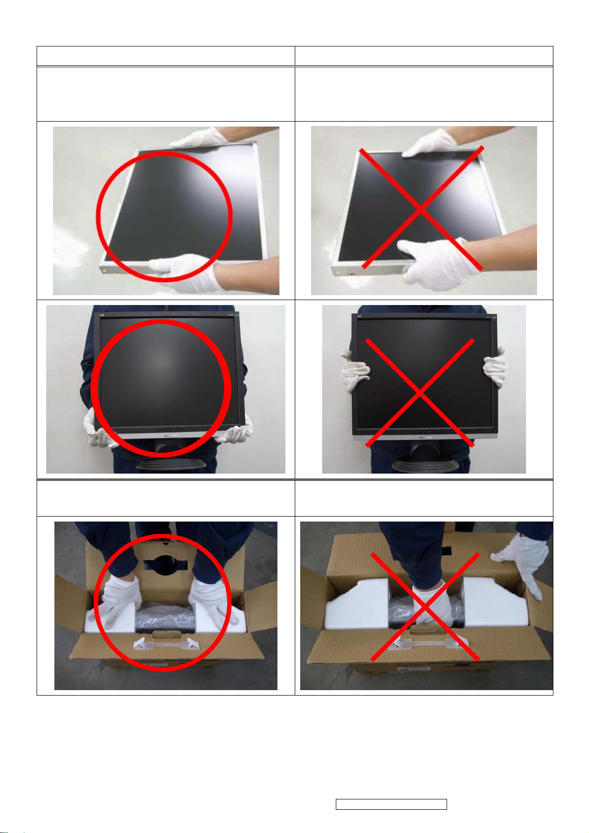
HANDING AND PLACING METHODS
Correct Methods: Incorrect Methods:
Only touch the metal frame of the LCD panel or
the front cover of the monitor. Do not touch the
surface of the polarizer.
Surface of the LCD panel is pressed by fingers
and that may cause “Mura.”
Take out the monitor with cushions
Taking out the monitor by grasping the LCD
panel. That may cause “Mura.”
ViewSonic Corporation
2
Confidential - Do Not Copy VP2650wb-1
Page 6
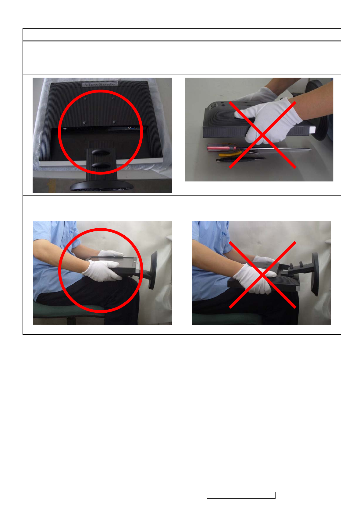
Correct Methods: Incorrect Methods:
Place the monitor on a clean and soft foam
pad.
Place the monitor on the lap, the panel surface
must be upwards.
Placing the monitor on foreign objects. That
could scratch the surface of the panel or cause
“Mura.”
The panel is placed facedown on the lap. That
may cause “Mura.”
ViewSonic Corporation
3
Confidential - Do Not Copy VP2650wb-1
Page 7
2. Specification
2.1 Product definition and specification
Product Name
Oracle P/N
Model Number
OSD Languages
TFT LCD Panel and Model #
Scalar
Input Signal
Sync Compatibility
ViewSonic VP2650Wb
VP2650WB
VP2650WB-EU
VP2650WB-CN
VS11997
English
French
German
Spanish
Italian
Finnish
Russian
Japanese
Korean
Traditional Chinese
Simplified Chinese
CPT CLAA260WU09
Genesis 5862H
Analog x1 / Digital x1
Separate Sync / Composite Sync / SOG
Adapter
Power Cable (Refer to APPENDIX B) Yes
15 pin mini D-SUB Analog Cable (1.8 m, black), with PC
2001 and Hot Plug Detect &DDC
(Detached cable; refer the Appendix A)
DVI-D Cable(1.8m, black) with PC 2001
(refer to Appendix A)
Audio Cable(1.8m, black) with PC 2001
MIC Cable(1.8m, black) with PC 2001
USB Cable (V2.0)
(1.8m, black) with PC 2001
English French
German Dutch
ViewSonic CD Wizard
Finnish Swedish
Italian Spanish
Internal Power Board
Yes
Yes
No
No
Yes
Greek Russian
Czech Hungarian
Turkish Polish
ViewSonic Quick Start Guide
Romania Bulgaria
Slovakia Croatia
Serbia Slovenia
ViewSonic Corporation
4
Confidential - Do Not Copy VP2650wb-1
Page 8
Portuguese Arabic
Japanese Traditional Chinese
Korean Simplified Chinese
Screen Protector Mylar Yes
Foot Protector plastic Yes, for left-front and right-front foot
Service Insert (Refer to Segment 5.9.3) For Region code = M units only
Vista Installation Guide Flyer
Yes
(Refer to Segment 5.9.1)
Energy Star Sticker (Refer to F8.2) Yes
POP Sticker (Refer to Segment 5.8.3) Yes
Warranty Card For Region code = G units only
Warranty Carton Sticker (refer to F8.1) For Region code = G units only
PE bag of Carton For Region code = G units only
ViewSonic Corporation
5
Confidential - Do Not Copy VP2650wb-1
Page 9
GENERAL specification
Test Resolution & Frequency 1920 x 1200 @ 60Hz
Test Image Size Full Size
Contrast and Brightness Controls
Factory Default:
Contrast = 70%, Brightness = 100%
VIDEO INTERFACE
Input Connector (refer the Appendix A) Analog = DB-15 (Analog)
Digital = DVI-D (Digital)
Default Input Connector Defaults to the first detected input
Video Cable Strain Relief Equal to twice the weight of the monitor for five minutes
Refer to Appendix A;
Video Cable Connector Pin out
Compliant DDC/2B and DDC/CI
Video RGB (Analog)
Video Signals
Separate Sync / Composite Sync / SOG
TMDS (Digital)
Video Impedance 75 Ohms (Analog), 100 Ohms (Digital)
Maximum PC Video Signal 950 mV with no damage to monitor
Maximum Mac Video Signal 1250 mV with no damage to monitor
Sync Signals TTL
Compliant with version 1.3;
DDC/2B
The DDC communication shall not interrupt when power
off.
Compliant with Revision 1.1;
DDC/CI
The DDC communication shall not interrupt when power
off.
Digital link protection HDCP
Sync Compatibility Separate Sync / Composite Sync / SOG
Shall be compatible with all PC type computers,
Video Compatibility
Macintosh computers, and after market video cards
Resolution Compatibility Refer to Segment 4-5
Exclusions Not compatible with interlaced video
USB INTERFACE
Up stream:
USB B type female connector x1
Connector
Power Source 5Vdc (internal power board; refer to segment 4.4)
Power saving function The USB function shall keep working under power saving mode as below,
ViewSonic Corporation
Down stream
USB A type female connector x4
6
Confidential - Do Not Copy VP2650wb-1
Page 10

Display mode USB Hub
On On
Power Saving On
Off Off
Compatibility USB 2.0 certified
ViewSonic Corporation
7
Confidential - Do Not Copy VP2650wb-1
Page 11
POWER SUPPLY
Internal Power Supply 5E.0DV02.001
Input Voltage Range 90 to 264 VAC
Input Frequency Range 47 to 63 Hertz
Short Circuit Protection Output can be shorted without safety issue
Over Current Protection 5.0A typical at 24VDC( Protect when short circuit)
Leakage Current 3.5mA (Max) at 264VAC / 60Hz
Efficiency (at 115VAC Full Load) 80% typical at 115Vac full load
Fuse Internal and not user replaceable
Power Output
<110 Watts (typ.)
< 64.5 Watts (Energy Star)
Max Input AC Current 1.5 Arms (max.)
80A Max./240Vac/50Hz
Inrush Current (Cold Start)
(Cold start 25℃ at full load)
Shall start and function properly when under full load, with
Power Supply Cold Start
all combinations of input voltage, input frequency, and
operating temperature.
Shall be able to withstand an ANSI/IEEE C62.41-1980
Power Supply Transient Immunity
6000V 200 ampere ring wave transient test with no
damage.
Shall be able to withstand ±1KV (L-L) and ±2KV (L-PE)
Power Supply Line Surge Immunity
(Refer to EN55024:1998 / CISPR24.1997 / IEC1000-4-5:
1995 / EN61000-4-5: 1995)
Shall be able to function properly, without reset or visible
Power Supply Missing Cycle Immunity
screen artifacts, when ½ cycle of AC power is randomly
missing at nominal input.
The power supply shall not produce audible noise that
would be detectable by the user. Audible shall defined to
Power Supply Acoustics
be in compliance with ISO 7779 (DIN EN27779:1991)
Noise measurements of machines acoustics. Power
Switch noise shall not be considered.
Power Saving Operation(Method) VESA DPMS Signaling
Mode LED Power Consumption
110 W (typ; No USB peripheral
plugged)
On Blue
Power Consumption
120 W (max; With full load USB
hub)
Active off Amber <2W
Off Off <1W
Recovery Time On Mode = N/A, Active Off < 3 sec
ViewSonic Corporation
8
Confidential - Do Not Copy VP2650wb-1
Page 12
ELECTRICAL REQUIREMENT
Horizontal / Vertical Frequency
Horizontal Frequency
Analog = 24 – 92 kHz
Digital = 31 – 92 kHz
Vertical Refresh Rate
50 – 85 Hz
Maximum Pixel Clock Analog = 195 MHz
Digital = 165 MHz
Sync Polarity Independent of sync polarity
Timing Table
Digital - TMDS
SOG
DMT
DMT
For SOG sync, switch 640x400@60Hz and
640x480@60Hz by [1]+[2] short cut key (primary =
Item Timing
640 x 350 @ 70 Hz, 31.5 KHz
640 x 400 @ 60 Hz, 31.5 KHz
Analog
Composite
Separated
Remark
640 x 400 @ 70 Hz, 31.5 KHz
640 x 480 @ 50 Hz, 24.7 KHz
640 x 480 @ 60 Hz, 31.5 KHz
640 x 480 @ 67 Hz, 35 KHz
640 x 480 @ 72 Hz, 37.9 KHz
640 x 480 @ 75 Hz, 37.5 KHz
640 x 480 @ 85 Hz, 43.3 KHz
640x480@60Hz)
DMT
For Separate, Composite and SOG, the image vertical
size image will be not full screen (Still at the center),
And the OSD will be 640x400/720x400 (promary=
640x400).
CVT
DMT
For SOG sync, switch 640x400@60Hz and
640x480@60Hz by [1]+[2] short cut key (primary =
640x480@60Hz)
For MAC
DMT
DMT
DMT
DMT
720 x 400 @ 70 Hz, 31.5 KHz
720 x 480 @ 60 Hz, 15.8 KHz
720 x 480 @ 60 Hz, 31.5 KHz
ViewSonic Corporation
For Separate, Composite and SOG, the image vertical
size image will be not full screen (Still at the center),
And the OSD will be 640x400/720x400 (promary=
640x400).
1. DTV 480i
2. Cause of interlace signal, the image might be flicker.
DTV 480p
9
Confidential - Do Not Copy VP2650wb-1
Page 13

720 x 576 @ 50 Hz, 15.8 KHz
1. DTV 576i
2. Cause of interlace signal, the image might be flicker.
720 x 576 @ 50 Hz, 31.3 KHz
800 x 600 @ 56 Hz, 35.2 KHz
800 x 600 @ 60 Hz, 37.9 KHz
800 x 600 @ 72 Hz, 48.1 KHz
800 x 600 @ 75 Hz, 46.9 KHz
800 x 600 @ 85 Hz, 53.7 KHz
832 x 624 @ 75 Hz, 49.7 KHz
1024 x 768 @ 50 Hz, 39.6 KHz
1024 x 768 @ 60 Hz, 48.4 KHz
1024 x 768 @ 70 Hz, 56.5 KHz
1024 x 768 @ 72 Hz, 58.1 KHz
1024 x 768 @ 75 Hz, 60 KHz
1024 x 768 @ 75 Hz, 60.2 KHz
1024 x 768 @ 85 Hz, 68.7 KHz
1152 x 864 @ 75 Hz, 67.5 KHz
1152 x 870 @ 75 Hz, 68.7 KHz
DTV 576p
DMT
DMT
DMT
DMT
DMT
MAC
CVT
DMT
DMT
DMT
DMT
For MAC
DMT
DMT
For MAC
1152 x 900 @ 67 Hz, 62.5 KHz
1280 x 720 @ 50 Hz, 37.5 KHz
1280 x 720 @ 60 Hz, 45 KHz
1280 x 768 @ 50 Hz, 39.6 KHz
1280 x 768 @ 60 Hz, 47.4 KHz
1280 x 768 @ 60 Hz, 47.8 KHz
1280 x 768 @ 75 Hz, 60.3 KHz
1280 x 768 @ 85 Hz, 68.6 KHz
1280 x 960 @ 50 Hz, 49.4 KHz
1280 x 960 @ 60 Hz, 60.0 KHz
1280 x 960 @ 75 Hz, 75.2 KHz
1280 x 960 @ 85 Hz, 86 KHz
1280 x
@ 50 Hz, 52.7 KHz
1024
For SUN
DTV 720p
DTV 720p
CVT
DMT;
DMT;
For Composite and SOG,
Switch 1280x768@60Hz and 1360x768@60Hz by
[1]+[2] short cut key (primary = 1280x768@60Hz)
DMT;
DMT;
DMT
DMT
DMT
DMT
DMT
1280 x
@ 60 Hz, 64 KHz
1024
1280 x
@ 75 Hz, 80 KHz
1024
1280 x
@ 85 Hz, 91 KHz
1024
10
ViewSonic Corporation
DMT
DMT
DMT
Confidential - Do Not Copy VP2650wb-1
Page 14
DMT;
1360 x 768 @ 60 Hz, 47.7 KHz
1440 x 900 @ 60 Hz 55.9 KHz
1440 x 900 @ 75 Hz 70.6 KHz
1400 x
@ 60 Hz 65.3 KHz
1050
1600 x
@ 60 Hz 75.0 KHz
1200
1680 x
@ 60 Hz 64.7 KHz
1050
1680 x
@ 60 Hz 65.3 KHz
1050
For Composite and SOG,
Switch 1280x768@60Hz and 1360x768@60Hz by
[1]+[2] short cut key (primary = 1280x768@60Hz)
DMT
DMT
1. DMT
2. No scaling function
(always full screen)
1. DMT
2. No scaling function
(always full screen)
1. DMT
2. No scaling function
(always full screen)
1. DMT
2. No scaling function
(always full screen)
1920x1080 @ 50 Hz 28.1 KHz
1920x1080 @ 50 Hz 56.25 KHz
1920x1080 @ 60 Hz 33.7 KHz
1920x1080 @ 60 Hz 67.5 KHz
1920x1200 @ 60 Hz 74 KHz
1. DTV 1080i
2. No scaling function
(always full screen)
3. Cause of interlace signal, the image might be flicker.
1. DTV 1080p
2. No scaling function
(always full screen)
1. DTV 1080i
2. No scaling function
(always full screen)
3. Cause of interlace signal, the image might be flicker.
1. DTV 1080p
2. No scaling function
(always full screen)
1. DMT
2. No scaling function
(always full screen)
1. DMT
1920x1200 @ 60 Hz 74.6 KHz
2. No scaling function
(always full screen)
*1. Tolerance ≧ ±2KHz. (if no over lapping issue)
*2. Any timing not in the list, it should display as normal or show on “OUT OF RANGE” OSD message without
blanking.
ViewSonic Corporation
11
Confidential - Do Not Copy VP2650wb-1
Page 15

Primary Presets
1920x1200 @ 60Hz
User Presets
Number of User Presets (recognized timings) Available: 10 presets total in FIFO configuration
Changing Modes
● Maximum Mode Change Blank Time for image stability : 3 seconds (Max), excluding “Auto
Adjust” time
● It should recall factory setting when execute Auto Image Adjust function by following
conditions,
1. Memory recall under DOS mode (640 x 350, 720 x 400 & 640 x 400).
2. New timing mode detected under DOS mode (640 x 350, 720 x 400 & 640 x 400).
● The monitor needs to do “Auto Adjust” the first time a new mode is detected
(see section “0-Touch™ Function Actions”)
● While running Change Mode, Auto Adjust or Memory Recall, the image shall blank
12
ViewSonic Corporation
Confidential - Do Not Copy VP2650wb-1
Page 16
TFT LCD PANEL
1st Source Panel
Model number CPT CLAA260WU09
Type Active Matrix TFT, TN technology
Active Size 550.08 mm x 343.8 mm (25.5” Wide)
Pixel Arrangement RGB Vertical Stripe
Pixel Pitch 0.2865 mm
Glass Treatment Anti-Glare
# of Backlights 6 CCFL
Backlight Life 50000 (6mA) Hrs (Min)
Luminance (Center) –
CT = 6500K,
Contrast/ Brightness = Max
Brightness Uniformity 75 % (Min)
Contrast Ratio DCR on (by scalar)
Color Depth 16.7 million colors (RGB 6 bit + Hi FRC)
Color Space NTSC 100% (CIE1931)
Horizontal Viewing Angle 160 degrees (Typ) / 140 degrees (Min) @ CR>10
Vertical Viewing Angle 160 degrees (Typ) / 140 degrees (Min) @ CR>10
Response Time
400 cd/m2 (Typ after 30 minute warm up)
300 cd/m2 (Min after 30 minute warm up)
4000 (Typ)
3500 (Min)
DCR off
1000 :1 (Typ)
800 : 1 (Min)
NTSC 110% (CIE1976)
On-Off (Raise + Fall)
Test conditions,
10%-90% @ Ta=25°C
Digital input
Contrast =Default
Brightness = Default
User Color (R/G/B=100%)
Mercury <5 mg per lamp
Panel Defects Please see Panel Quality Specifications.
*The average of measured value from monthly shipment shall be equal or better than the Typical value above.
ViewSonic Corporation
5ms (typ) / 8ms (max)
GTG (OD by scalar; base on)
3ms (Avg)
5ms (max)
*GTG Test conditions
1. 64x64 matrix
2. Analog or Digital input
3. Brightness OSD = 100
4. Contrast OSD = 100
5. Color = User Color (R/G/B = 100)
13
Confidential - Do Not Copy VP2650wb-1
Page 17

EDID data
VP2650wb_Analog.ddc
00 FF FF FF FF FF FF 00
5A 63 20 EB 01 01 01 01
01 12 01 03 0E 37 22 78
2E 70 25 AB 51 36 B3 24
10 50 54 BF EF 80 B3 00
A9 40 90 40 81 80 81 40
31 59 01 01 01 01 28 3C
80 A0 70 B0 23 40 30 20
36 00 26 58 21 00 00 1A
00 00 00 FF 00 51 56 30
30 38 30 31 30 30 30 30
31 0A 00 00 00 FD 00 32
55 18 5C 14 00 0A 20 20
20 20 20 20 00 00 00 FC
00 56 50 32 36 35 30 77
62 0A 20 20 20 20 00 52
VP2650wb_DVI.ddc
00 FF FF FF FF FF FF 00
5A 63 20 EB 01 01 01 01
01 12 01 03 80 37 22 78
2E 70 25 AB 51 36 B3 24
10 50 54 BF EF 80 31 0A
B3 00 A9 40 90 40 81 80
81 40 71 4F 31 59 28 3C
80 A0 70 B0 23 40 30 20
36 00 26 58 21 00 00 1A
00 00 00 FF 00 51 56 30
30 38 30 31 30 30 30 30
31 0A 00 00 00 FD 00 32
55 1F 5C 11 00 0A 20 20
20 20 20 20 00 00 00 FC
00 56 50 32 36 35 30 77
62 0A 20 20 20 20 00 E5
14
ViewSonic Corporation
Confidential - Do Not Copy VP2650wb-1
Page 18
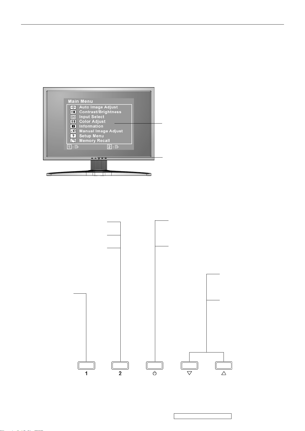
3. Front Panel Function Control Description
Adjusting the Screen Image
Main Menu
with OSD controls
Front Control Panel
shown below in detail
Displays the control screen
for the highlighted control.
Also toggles between two
controls on some screens.
Also a shortcut to toggle
analog and digital
connection.
Displays the
Main Menu or
exits the
control screen
and saves
adjustments.
Power light
Blue = ON
Orange = Power Saving
Standby Power
On/Off
Scrolls through
menu options and
adjusts the
displayed control.
Also a shortcut to
display the
Contrast
adjustment control
screen.
15
ViewSonic Corporation
Confidential - Do Not Copy VP2650wb-1
Page 19
Do the following to adjust the display setting:
1. To display the Main Menu, press button [1].
NOTE: All OSD menus and adjustment screens disappear automatically after about 15
seconds. This is adjustable through the OSD timeout setting in the setup menu.
2. To select a control to adjust, pressSorTto scroll up or down in the Main Menu.
3. After the desired control is selected, press button [2]. A control screen like the one shown
below appears.
The line at the bottom of the screen shows
the current functions of buttons 1 and 2:
Exit or select the Brightness control.
4. To adjust the control, press the up S or down T buttons.
5. To save the adjustments and exit the menu, press button [1] twice.
The following tips may help you optimize your display:
• Adjust the computer's graphics card so that it outputs a 1920 x 1200 @ 60Hz video signal to
the LCD display. (Look for instructions on “changing the refresh rate” in the graphics card's
user guide.)
• If necessary, make small adjustments using H. POSITION and V. POSITION until the
screen image is completely visible. (The black border around the edge of the screen should
barely touch the illuminated “active area” of the LCD display.)
16
ViewSonic Corporation
Confidential - Do Not Copy VP2650wb-1
Page 20
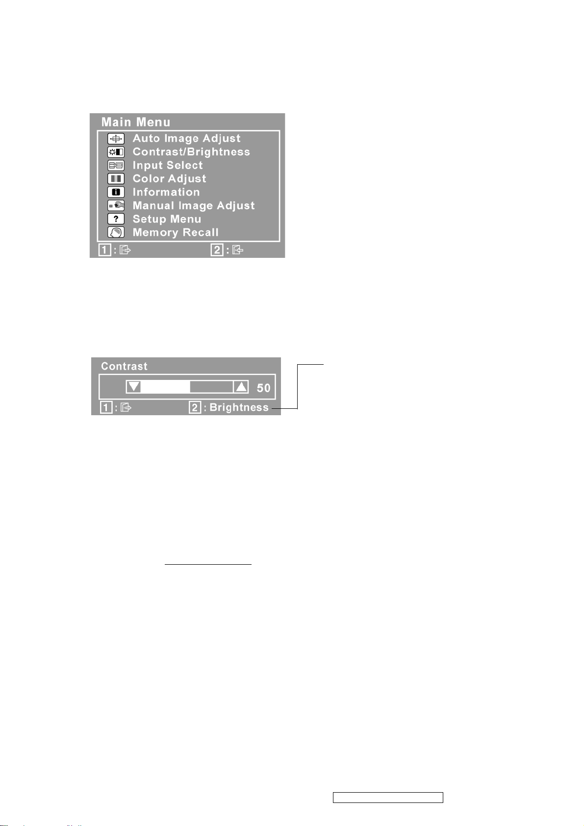
Main Menu Controls
Adjust the menu items shown below by using the up S and down T buttons.
Control Explanation
Auto Image Adjust automatically sizes, centers, and fine tunes the video signal
to eliminate waviness and distortion. Press the [2] button to obtain a sharper
image.
NOTE: Auto Image Adjust works with most common video cards. If this
function does not work on your LCD display, then lower the video refresh rate
to 60 Hz and set the resolution to its pre-set value.
Contrast adjusts the difference between the image background (black level)
and the foreground (white level).
Brightness adjusts background black level of the screen image.
Input Select toggles between inputs if you have more than one computer
connected to the LCD Display.
Color Adjust provides several color adjustment modes, including preset color
temperatures and a User Color mode which allows independent adjustment of
red (R), green (G), and blue (B). The factory setting for this product is 6500K
(6500 Kelvin).
sRGB-This is quickly becoming the industry standard for color management,
with support being included in many of the latest applications. Enabling this
setting allows the LCD display to more accurately display colors the way they
were originally intended. Enabling the sRGB setting will cause the Contrast and
Brightness adjustments to be disabled.
9300K-Adds blue to the screen image for cooler white (used in most office
settings with fluorescent lighting).
17
ViewSonic Corporation
Confidential - Do Not Copy VP2650wb-1
Page 21

Control Explanation
7500K-Adds blue to the screen image for cooler white (used in most office
settings with fluorescent lighting).
6500K-Adds red to the screen image for warmer white and richer red.
5000K-Adds red to the screen image for warmer white and richer red.
User Color Individual adjustments for red (R), green (G), and blue (B).
1. To select color (R, G or B) press button [2].
2. To adjust selected color, pressSandT.
Important: If you select RECALL from the Main Menu when the product is
set to a Preset Timing Mode, colors return to the 6500K factory preset.
Information displays the timing mode (video signal input) coming from the
graphics card in the computer, the LCD model number, the serial number, and
the ViewSonic® website URL. See your graphics card’s user guide for
instructions on changing the resolution and refresh rate (vertical frequency).
NOTE: VESA 1920 x 1200 @ 60Hz (recommended) means that the resolution
is 1920 x 1200 and the refresh rate is 60 Hertz.
Manual Image Adjust displays the Manual Image Adjust menu.
H./V. Position (Horizontal/Vertical Position) moves the screen image left or
right and up or down.
H. Size (Horizontal Size) adjusts the width of the screen image.
18
ViewSonic Corporation
Confidential - Do Not Copy VP2650wb-1
Page 22
Control Explanation
Fine Tune sharpens the focus by aligning text and/or graphics with pixel
boundaries.
NOTE: Try Auto Image Adjust first.
Sharpness adjusts the clarity and focus of the screen image.
Dynamic Contrast allows the user to turn the contrast ratio enhancement on or
off.
Aspect ratio Selects the image size for 1:1, fill aspect ratio & full screen.
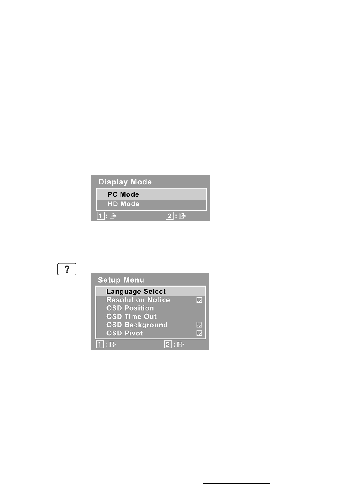
Display Mode provides two color space modes. The factory setting for this
product is PC mode.
PC mode sets color space to RGB for PC timing mode.
HD mode sets color space to YUV for HD timing mode.
Setup Menu displays the menu shown below:
19
ViewSonic Corporation
Confidential - Do Not Copy VP2650wb-1
Page 23

Control Explanation
Language Select allows the user to choose the language used in the menus and
control screens.
Resolution Notice advises the optimal resolution to use.
OSD Position allows the user to move the OSD menus and control screens.
OSD Timeout sets the length of time the OSD screen is displayed. For
example, with a “15 second” setting, if a control is not pushed within 15
seconds, the display screen disappears.
OSD Background allows the user to turn the OSD background On or Off.
OSD Pivot is used to rotate the OSD menu, changing the OSD screen to
Landscape or Portrait mode.
Memory Recall returns the adjustments back to factory settings if the display is
operating in a factory Preset Timing Mode listed in the Specifications of this
manual.
Exception: This control does not affect changes made with the Language
Select or Power Lock setting.
OSD and Power Lock Settings
• OSD Lock: Press and hold [1] and the up arrow S for 10 seconds. If any buttons are
pressed the message OSD Locked will display for 5 seconds.
• OSD Unlock: Press and hold [1] and the up arrow S again for 10 seconds.
• Power Button Lock: Press and hold [1] and the down arrow T for 10 seconds. If the
power button is pressed the message Power Button Locked will display for 5 seconds. With
or without this setting, after a power failure, your LCD display’s power will automatically
turn ON when power is restored.
• Power Button Unlock: Press and hold [1] and the down arrow T again for 10 seconds.
20
ViewSonic Corporation
Confidential - Do Not Copy VP2650wb-1
Page 24

4. Circuit Description
I. Introduction:
The VP2650wb is a 25.5" (1920x1200) TFT LCD monitor. It’s a dual interface (include
analog and digital) and support USB function ( 4 port) and OSD Pivot function and support
over-driver function LCD monitor and it’s compliant with VESA specification to offer a smart
power management and power saving function.
It also offers OSD menu for users to control the adjustable items and get some information
about this monitor. The VP2650wb also offers DDC/CI function to meet VESA standard and DVI
with HDCP function.
II. Circuit Implementations:
A.) THE MAIN BODY:
A-1.) Interface board block diagram:
SDRAM
Digital
OSD
Pivot
DDC
Digital
Diff Data & Clock
(D)
Analog
D-SUB
DSUB R,G, B
HS, VS
Analog
DDC
(a) Circuit operations:
In analog signal input to scaling IC, the operation theory is to convert the analog
GM5862H
A/D&TMDS&
Scaling& MCU
&OSD&HDCP
Flash
Rom
EEPROM
(HDCP)
USB BD.
CTRL BD.
To LCD
MODULE
DRIVING
Block
signals of Red, Green and Blue to the digital signals of Red, Green and Blue. The scaling
IC has the internal A/D converter that converts analog signals to digital data.
The scaling IC has OSD and auto detecting input timing functions. OSD offers adjustable
functions to the end-users. Auto detecting timing function can detect change modes. It
outputs the digital R-G-B data, pixel clock and control signal to TCON of the LCD module. A
MCU, build in scaling IC (Genesis GM5862H-LF), is responsible for the system processing.
There are two external storing units, one is 24C16 to store the OSD function data and user
preset timings and HDCP key content, the other one is flash ROM (25LV040) to store the
21
ViewSonic Corporation
Confidential - Do Not Copy VP2650wb-1
Page 25

firmware code.
Others, the scalar IC has a I/O port to detect Pivot device whether its level change, once
I/O port level change, the scalar will auto make OSD Menu window disappear.
Moreover, when input timing VS over 75Hz, the scalar will along with external SDRAM
memory to do FRC function, and make image can work normally.
(b) IC introduction:
1.) Genesis GM5862H-LF SCALER IC:
Genesis GM5862H with analog (RGB), DVI and HDCP function, and support
resolution up to WUXGA. The gm5862H leverages Genesis patented advanced
image-processing technology, as well as a proven integrated ADC/PLL and an
Ultra-Reliable DVI® compliant digital receiver to deliver a high-quality solution for
mainstream dual input monitors. The gm5862H also includes an ITU656 video input port
with color space converter that makes it an attractive solution for low cost MFM and TV
applications. The output section contains a 24-bit TTL output interface and a dual
channel LVDS transmitter for direct interfacing of commercially available LVDS LCD
panel modules. In addition, GM5862H includes an integrated X86 OCM with SPI
compatible interface, advanced color control features, a multicolor proportional font OSD
engine, and a number of system I/O components.
2.) EEPROM:
Use 24C16 EEPROM to store monitor user data and user preset timings and
HDCP key. There are 10 user timing modes are automatically saved in it. Each timing
mode is allocated with 22 bytes of memory space for information such as Sync
frequencies, polarities… etc. PC can access the EEPROM data indirectly through the
SDA and SCL channels of DVI and D-sub (IIC communication). The digital and analog
DDC data are stored in two 24C02s EEPROM.
3.) Flash:
Use 25LV040 flash rom to save firmware program in order that the scalar IC
GM5862H
can access code from it and deal with it by CPU engine within the scalar.
22
ViewSonic Corporation
Confidential - Do Not Copy VP2650wb-1
Page 26
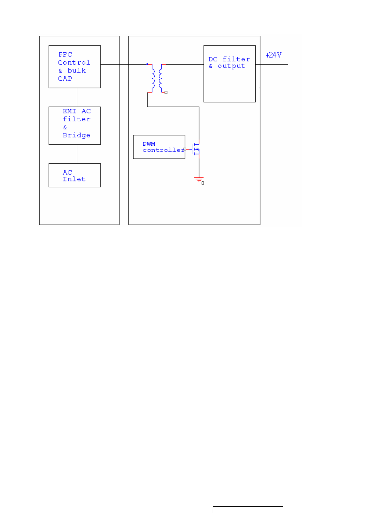
A-2.) Power board diagram:
The power board have two function blocks , one is power factor correction ( PFC ), the other
one is PWM to get DC output .
A-3.) PFC circuit introduction :
IC651( L6562) is a preregulator for power factor correction . The function and circuit is similar
to step-up stage.
It can boost low AC input voltage to bulk capacitor to get higher power factor.
Pin 1. is the inverting input of the error amplifier. R671,R672,R673,R674 are resistive divider
and are connected brtween the output regulated voltage and this point , to provide voltage
feedback.
Pin 2. is the output of amplifier. A feedback compensation network is placed between this pin
and the Pin 1.
Pin 3. is the input of the multiplier stage. R657,R658,R659 are resistive divider and are
connected to this pin the rectified mains . A voltage signal , proportional to the rectifed mains ,
appears on this pin .
Pin 4. is the input to the comparator of the control loop . The current is sensed by resistor
R670 and the resulting voltage is applied to this pin .
Pin 5. is the zero current detection input . If it is connected to GND , the device will be
disabled.
Pin 6. is the current return for driver and control circuits .
Pin 7. is the gate driver output . A push pull output stage is able to drive the power MOS .
Pin 8. is supply voltage of driver and control circuits.
ViewSonic Corporation
23
Confidential - Do Not Copy VP2650wb-1
Page 27
R657
1M F
R658
1M F
R660
1M F
R661
1M F
R662
511K F
E1
A10
IC651
8
VCC
3
MULT
2
R659
C621
20K F
0.01U K
C620
1U K
A8 A9
12
C622
+
1U 100V
<Spec>
6
L6562N
1 2
1 2
2.2U K
COMP
GND
C623
2.2U K
10V
C624
10V
+
+
L6562N
ZD652
TZMC 24
ZCD
GD
CS
INV
C625
0.1U K
R664
3.01K F
AK
5
7
4
1
D651
A K
1N5406
T651
390U
2
7 9
R667
68K
R668
30
D655
LL4148
E3
11
A3
AK
A4
R655
10K
C628
1U
G
A1
R669
1K J
C626
470P K
R663
205K F
D652
A K
YG971S6R
D
Q651
2SK3502
S
A2
R670
0.22
R666
22.6K F
R665
47
D
Q653
2N7002K-T1-E3
G
S
A-4.) PWM circuit introduction :
IC601 ( NCP1203) is the PWM control IC to get stable DC output. It can transfer high DC
12
+
c605
150U 450V M
<Spec>
E2
B+
R671
499K F
R672
232K F
R673
232K F
R674
8.25K F
voltage at primary to low DC voltage at secondary .
Pin 1. lets user adjutst the lavel at which the cycle skipping process takes place . Shorting this
pin to ground , permanently disables the skip cycle feature.
Pin 2. is connected to optocoupler , the peak current setpoint is adjusted accordingly to the
output power demand .
Pin 3. senses the primary current and routes it to the internal comparator .
Pin 4. is the IC ground .
Pin 5. is the driver’s output pin to an external MOSFET .
Pin 6. is Vcc pin and connected to an external bulk capacitor .
Pin 7. is empty and ensures adequate creepage distance .
Pin 8. is connected to the high-voltage rail , this pin injects a constant current into the Vcc bulk
capacitor .
24
ViewSonic Corporation
Confidential - Do Not Copy VP2650wb-1
Page 28

R607
C607
68K
D601
UF4007-LF
A K
L611
Z45/100MHZ
D602
EGP10D-LF
D
Q601
2SK3548-01SC
S
R615
0.22
680P K
E5
AK
N5
43
C610
1000P K
R617
10K J
R608
1M F
R609
1M F
IC601NCP1203P40G
‧
1
ADJ
2
FB
3
CS
4
GND
D610
A K
RSX101VA-30
R613
1K J
R610
18K
R603
10K
D611
UF4007-LF
A K
A11
R611
D603
8
HV
7
NC
6
VCC
5
DRV
D608
RSX101VA-30
C613
0.1U K
D609
A K
RSX101VA-30
R623
A K
4.7 J
R612
47
D605
R619
18K
LL4148
A K
C609
1000P K
150 J
12
ZD601
C611
+
TZMC15
47U 50V
A K
D604
AK
LL4148
LL4148
R614
18K
AK
12
C606
+
47U 50V
G
A12
A-5.) Buck Converter(MCU, USB, Audio, Panel Power section)
T601
2
3
1
5 8
540UH
R712
2K
IC602
PC123FY 1J00F
12
R
A K
9
10
7
IC702
KA431AZTA_NL
R714
1K J
D703
A2
YG865C15R
J
A1
D702
A2
YG865C15R
J
A1
D701
A2
YG865C15R
J
A1
R705
10
C709
C710
1000P K
C716
0.1U K
1000P K
R706
10
R713
10K
R716
28K F
R715
2.61K F
12
+
C711
470U 35V
Fig.A
Fig.A shows the typical Buck Converter circuit. Q2 s a switching device, and Q1, Q4 are the
totem pole which get enough ability to drive P-MOS. When the Gtae of Q2 is low level, Q2
turns on. At high level, Q2 turns off. The pulse waveform will appear at D-terminal of Q2. L1,
C5, C6, and D1 will transfer the pulse to stable DC level.
The feedback circuit is composed of two resistors R5 and R11, and feedback the DC level
1.25V with error signal. C8 is a compensation capacitor.
ViewSonic Corporation
25
Confidential - Do Not Copy VP2650wb-1
Page 29

A-6.) PWM IC (TL1451)
Fig. 2
The Tl1451AC incorporates on a single monolithic chip all the functions required in the
construction of two pulse-width modulation control circuits. Designed primarily for power
supply control, the TL1451AC contains an on-chip 2.5V regulator two error amplifiers, an
adjustable oscillator, two dead-time comparators, under-voltage lockout circuitry, and dual
common-emitter output transistor circuits. The uncommitted output transistors provide
common-emitter output capability for each controller. The internal amplifiers exhibit a
common-mode voltage range from 1.04V to 1.45V. The dead-time control comparator has no
offset unless externally altered and can provide 0% to 100% dead time. The on-chip oscillator
can be operated by modulating RT and CT. During low Vcc conditions, the under-voltage
lockout control circuit feature locks the outputs off until the internal circuitry is operational.
ViewSonic Corporation
26
Confidential - Do Not Copy VP2650wb-1
Page 30

5. Adjustment Procedure
1. Alignment procedure (for function adjustment)
A list of necessary alignments for the LCD monitor:
Items Description Remark
1 Timing adjustment Preset timing
2 Auto color balance adjustment Timing 114
VGA 480 640x480@60Hz
Pattern 42(5-Mosaic)
3 Color temperature adjustment 1=C1/9300/Bluish,
2=C2/6500/sRGB/,
3=C3/5000/Reddish,
4=User, 5=Cx, 6=Cx2
4 Writing EDID file Analog
A. Preparation:
1. Setup input timing to 640x480@60Hz and 5-Mosaic pattern (pattern 42).
2. Enter factory mode (first press “2”and then press “[ ]” button to turn on monitor).
3. Setup color at User color and “Burn in mode” =“ON”
4. Turn off the monitor, remove the input source and then power on again.
5. Setup unit and keep it warm up for at least 30 minutes.
B. Geometry adjustment & checking (for preset timing modes)
1. Enter factory mode (first press “2”and then press “[ ]” button to turn on monitor).
2. Run “Clear User” to erase user settings.
3. Select timing mode from Figure-1 and input full screen display pattern to monitor.
4. Enter OSD to run “Auto Image Adjust” function for geometry adjustment.
5. Check if the H/V position, Fine Tune and Horizontal Size of the image are ok or
acceptable to make sure function and performance are ok.
6. Run “Clear User” to erase user settings.
7. Turn off the monitor power.
8. Turn on the monitor power again to check if monitor’s image settings are ok and with
following settings.
CONTRAST = 70
BRIGHTNESS = 100
COLOR = 6500K (default setting)
27
ViewSonic Corporation
Confidential - Do Not Copy VP2650wb-1
Page 31

C. ADC calibration (Auto color balance adjustment)
~~Analog only, it is not required for DVI-D input source
1. Setup input timing VGA480 (640x480@60Hz), pattern 42(5-Mosaic pattern) with white
color frame with Analog signals from Chroma video pattern generator.
2. Enter factory mode (first press “2”and then press “[ ]” button to turn on monitor).
3. Setup color at User color and “Burn in mode” =“ON”
4. Press“ Auto” button to do white balance for auto color balance adjustment (will get
optimal gain / offset (clamp) values).
5. Checking if the picture is ok, or reject this monitor and check its circuit board or
wire/cable connection.
D. Color temperature adjustment
1. Setup input timing to any preset modes, pattern 41(full white color pattern) with Analog
signals from Chroma video pattern generator.
2. Enter factory mode (first press “2”and then press “[ ]” button to turn on monitor).
3. Setup color at User color and “Burn in mode” =“ON”
4. Make sure ADC calibration (auto color balance adjustment) had already been done.
5. First measure every Monitor native color temp. Luminance at Brightness and Contrast
(100/100) condition, so that other color temp. luminance can adjust by below condition.
Lv (Max) –Condition:
Brightness = 100 / Contrast = 100
CCT = USER COLOR (R/G/B=100%)
Lv (Srgb) –Condition:
CCT = sRGB
Lv (6500K) –Condition:
Brightness / Contrast = Default (100/70)
CCT = 6500K
Lv (9300K) –Condition:
Brightness / Contrast = Default(100/70)
CCT = 9300K
Lv (7500K) –Condition:
Brightness / Contrast = Default(100/70)
CCT = 7500K
Lv (5000K) –Condition:
Lv (Max) = The Luminance requirement of section 4-8
“TFT LCD PANEL”
120 ~ 150 nits
Lv (6500K) / Lv (Max) x 100% > 85%
Lv (9300K) / Lv (Max) x 100% > 65%
Lv (7500K) / Lv (Max) x 100% > 75%
Brightness / Contrast = Default(100/70)
CCT = 5000K
Lv (Brightness) –Condition:
Contrast = 100%
Lv (Contrast) –Condition: Lv(Contrast=0%) / Lv(Contrast=100%) x 100% 30%
28
ViewSonic Corporation
Lv (5000K) / Lv (Max) x 100% > 75%
Lv(Brightness=0%) / Lv(Brightness=100%) x 100%
55%
Confidential - Do Not Copy VP2650wb-1
Page 32

1. Measure each color temperature (C1, C2, C3, C4) by Minolta CA-110 (or equivalent
equipment).
2. Two methods can be used to adjust RED, GREEN, BLUE value of each color temperature,
C1, C2 & C3 to meet following spec requirement, the 1
IIC alignment protocol to do automatic adjustment, and the 2nd method is by manually and
must be in factory mode.
x+/- 0.283+/- 0.008 Color temperature
st
method is by using external PC and
(C1:9300K set on OSD)
y+- 0.297+/- 0.008
x+- 0.299+/- 0.008 Color temperature
(C2:7500K set on OSD)
y+- 0.315+/- 0.008
x+- 0.313+/- 0.008 Color temperature
(C3:6500K set on OSD)
y+- 0.329+/- 0.008
x+- 0.313+/- 0.008 Color temperature
(C3:sRGB set on OSD)
y+- 0.329+/- 0.008
x+- 0.345+/- 0.008 Color temperature
(C4:5000K set on OSD)
y+- 0.362+/- 0.008
Move cursor into “Clear User” tag and run to disable burn-in mode.
3. Turns off the monitor power.
Preset Color Temperatures
sRGB It should meet IEC 61966-2-1 (1999-10) standard.
Preset 1
CCT (typ) = 9300K (u’CCT=0.1888; v’ CCT=0.4457)
Δu’v’<0.01 (@ Full White pattern)
Preset 2
CCT (typ) = 7500K (u’CCT=0.1935; v’ CCT=0.4586)
Δu’v’<0.01 (@ Full White pattern)
Preset 3 (Primary)
CCT (typ) = 6500K (u’CCT=0.1978; v’ CCT=0.4684)
Δu’v’<0.01 (@ Full White pattern)
Preset 4
CCT (typ) = 5000K (u’
CCT=0.2044; v’ CCT=0.4808)
Δu’v’<0.01 (@ Full White pattern)
Preset Color Temperature
Adjustability
*Any gray level and Contrast/Brightness should not get reddish, greenish or bluish.
Each color preset shall be adjustable. Red, Green,
and Blue shall be individually controlled.
29
ViewSonic Corporation
Confidential - Do Not Copy VP2650wb-1
Page 33

Saturation
Contrast = Default
No visible saturation
Brightness = Default
Test pattern = 64-gray
Contrast = 100%
Brightness = 100%
6~8- level saturation
Test pattern = 32-gray
Contrast Ratio
CR(Max) –Condition:
Same as the Contrast Ratio in section 4-8 “TFT LCD
Contrast / Brightness = 100%
PANE L”
CCT = USER COLOR (R/G/B=100%)
CR(6500K) –Condition:
Contrast / Brightness = Default
CR(6500K) / CR(Max) ≧ 85%
CCT = 6500K
≧50% units of shipment shall be equal or better than typical CR s
E. Writing EDID data into monitor
1. Setup a PC with DDC card.
2. Connect PC to monitor with a D-sub signal cable.
3. Please refer to the C212 for the correct EDID file.
4. Runs the writing program to write the analog EDID data into EEPROM for analog input
(ie. 15-pin D-sub).
5. Repeat step 4 and write the digital EDID data into EEPROM for DVI-D input (ie. 24-pin
DVI-D).
6. Repeat step 4 and write the HDMI EDID data into EEPROM for HDMI input (ie. 19-pin
HDMI).
7. Read both EEPROM data and confirm it to match with the C212 definition. (Note: The
DVI-D input may not operation correctly if the digital EDID data do not exist.)
8. Download HDCP key to EEPROM from address 0X0600 (refer to EEPROM mapping).
30
ViewSonic Corporation
Confidential - Do Not Copy VP2650wb-1
Page 34

F. Command definition
PC Host will send 0x7C IIC slave address and then following 4 bytes command
Don’t
I2C Send Command Byte1 Byte2 Byte3 Byte4
Write Contrast to MCU RAM CA 55 Data cksum
Write Brightness to MCU RAM CA 56 Data cksum
Write Red Gain to MCU RAM CA 57 Data cksum
Write Green Gain to MCU RAM CA 58 Data cksum
Write Blue Gain to MCU RAM CA 59 Data cksum
Write s-Brightness data CA 9C Data cksum
Read Contrast from MCU RAM C3 55 XX cksum
Read Brightness from MCU RAM C3 56 XX cksum
Read Red Gain from MCU RAM by color
index C3 57 XX cksum
Read Green Gain from MCU RAM by color
index C3 58 XX cksum
Read Blue Gain from MCU RAM by color
index C3 59 XX cksum
Read F/W version from MCU’s constant
definition C3 5A XX cksum
Read panel vender from MCU’s constant
definition C3 5B XX cksum
Read Product ID C3 5C XX cksum
Read s-Brightness data C3 9C XX cksum
Write C1 (Bluish) R-Gain Data to EEPROM AA 3C Data cksum
Write C1 (Bluish) G-Gain Data to EEPROM AA 3D Data cksum
Write C1 (Bluish) B-Gain Data to EEPROM AA 3E Data cksum
Write C2 (sRGB) R-Gain Data to EEPROM AA 4C Data cksum
Write C2 (sRGB) G-Gain Data to EEPROM AA 4D Data cksum
Write C2 (sRGB) B-Gain Data to EEPROM AA 4E Data cksum
Write C3 (Reddish) R-Gain Data to
EEPROM
Write C3 (Reddish) G-Gain Data to
EEPROM
Write C3 (Reddish) B-Gain Data to
EEPROM
Write User R-Gain Data to EEPROM AA 6C Data cksum X
Write User G-Gain Data to EEPROM AA 6D Data cksum X
Write User B-Gain Data to EEPROM AA 6E Data cksum X
Write Cx R-Gain Data to EEPROM AA 7C Data cksum
Write Cx G-Gain Data to EEPROM AA 7D Data cksum
Write Cx B-Gain Data to EEPROM AA 7E Data cksum
Write Cx2 R-Gain Data to EEPROM AA 8C Data Cksum
Write Cx2 R-Gain Data to EEPROM AA 8D Data Cksum
Write Cx2 R-Gain Data to EEPROM AA 8E Data Cksum
Write Contrast to EEPROM AA 92 Data Cksum
Write Brightness to EEPROM AA 93 Data Cksum
Write C/T index to EEPROM AA 94 1~6 cksum
Write OSD-Hpos to EEPROM AA 95 Data cksum
Write OSD-Vpos to EEPROM AA 96 Data cksum
AA 5C Data cksum
AA 5D Data cksum
AA 5E Data cksum
Must
care
√
√
√
√
√
?
√
√
√
√
√
√
√
√
?
√
√
√
√
√
√
√
√
√
√
By
√
model Reserved for some model have
√
√
√
√
X
X
√
X
X
Note
Write data to MCU RAM and
update the related register to
refresh the screen immediately.
Don’t store data to EEPROM.
Set brightness default of
PWM( may not match OSD)
<Note H>
Base on current color index to
read back the right gain value.
Please see <Note F> for detail
implementation
Please see <Note G> for detail
implementation
Reply EDID(analog if dual
inputs) address 0A
Set brightness default of
PWM( may not match OSD)
<Note H>
extra color temperature
1=C1/9300/Bluish,
2=C2/6500/sRGB/,
3=C3/5500/Reddish,
4=User, 5=Cx, 6=Cx2
31
ViewSonic Corporation
Confidential - Do Not Copy VP2650wb-1
Page 35

0=DE, 1=EN, 2=ES, 3=FR,
For Viewsonic model
Write Language to EEPROM
AA 97 0~10 cksum
√
4=IT, 5=JA, 6=繁中, 7=簡中
(Also Update MCU RAM)
(Change Language type first)
0=EN, 1=Korea, 2=Turkish,
3=JA, 4=繁中, 5=簡中
Write Language to EEPROM (For Asia) AA 97 0~5 cksum
(Also Update MCU RAM)
(Change Language type first)
0=EN, 6=French, 7=Deutsch,
8=Italian, 9=Spanish,
0A=Hungarian, 0B=Serbian,
0C=Russian, 0D=Dutch,
0E=Polish, 0F=Czech,
10=Swedish, 11=Portugese,
12=Romanian
Write Language to EEPROM (For Europe) AA 97 6~12 cksum
Change Language type to Asia D1 AA XX cksum
(Also Update MCU RAM)
For Viewsonic model
Change Language Type to Europe
D1 XX* XX cksum
Write EEPROM OSD Timer AA 98 Data cksum
Write EEPROM Volume AA 99 Data cksum
√
XX* = Non “AA” value
X
For model with Gamma curve
selection function
0: By-pass
1: Enable
Write EEPROM Gamma index AA 9A Data cksum
Keep
Others: Impermissible
Set brightness default of
PWM( may not match OSD)
Write EEPROM brightness default AA 9C Data cksum
Write OSD Transparency to EEPROM AA 9E Data cksum
Write OSD Rotation to EEPROM AA 9F Data cksum
X
<Note H>
X
X
Range: 0~2
Write URL setting to EEPROM AA A0 Data cksum
?
Others: Impermissible
0: OSD
1: OSM
Write OSD/OSM setting to EEPROM AA A1 Data cksum
?
Others: Impermissible
0: Disable first auto
1: Enable first auto
Write First Auto setting to EEPROM AA A2 Data cksum
?
Others: Impermissible
0: English
Write “Factory Page Language” setting to
EEPROM
AA A3 Data cksum
?
5: Japanese
Others: Impermissible
Read C1 (Bluish) R-Gain data from
EEPROM
A3 3C XX cksum
√
Read C1 (Bluish) G-Gain data from
EEPROM
A3 3D XX cksum
√
Read C1 (Bluish) B-Gain data from
EEPROM
A3 3E XX cksum
√
Read C2 (sRGB) R-Gain data from
EEPROM
A3 4C XX cksum
√
Read C2 (sRGB) G-Gain data from
EEPROM
A3 4D XX cksum
√
Read C2 (sRGB) B-Gain data from
EEPROM
A3 4E XX cksum
√
Read C3 (Reddish) R-Gain data from
EEPROM
A3 5C XX cksum
√
Read C3 (Reddish) G-Gain data from
EEPROM
A3 5D XX cksum
√
Read C3 (Reddish) B-Gain data from
EEPROM
A3 5E XX cksum
√
Read User R-Gain data from EEPROM A3 6C XX cksum X
32
ViewSonic Corporation
Confidential - Do Not Copy VP2650wb-1
Page 36

Read User G-Gain data from EEPROM A3 6D XX cksum X
Read User B-Gain data from EEPROM A3 6E XX cksum X
Mode
Read Cx R-Gain data from EEPROM A3 7C XX cksum
l
Mode
Read Cx G-Gain data from EEPROM A3 7D XX cksum
Read Cx B-Gain data from EEPROM A3 7E XX cksum
Read Contrast from EEPROM A3 92 XX cksum
Read Brightness from EEPROM A3 93 XX cksum
√
√
l
Reserved for some model have
Mode
extra color temperature
l
1=C1/9300/Bluish,
2=C2/6500/sRGB/,
3=C3/5800/Reddish,
Read C/T index from EEPROM A3 94 XX cksum
Read OSD-Hpos EEPROM A3 95 XX cksum
Read OSD-Vpos from EEPROM A3 96 XX cksum
For Viewsonic model
Read Language from EEPROM
A3 97 XX cksum
√
√
√
√
4=User, 5=Cx
0=DE, 1=EN, 2=ES, 3=FR,
4=IT, 5=JA, 6=繁中, 7=簡中
0=EN, 1=Korea, 2=Turkish,
Read Language to EEPROM (For Asia) A3 97 0~5 cksum
3=JA, 4=繁中, 5=簡中
0=EN, 6=French, 7=Deutsch,
8=Italian, 9=Spanish,
0A=Hungarian, 0B=Serbian,
0C=Russian, 0D=Dutch,
0E=Polish, 0F=Czech,
10=Swedish, 11=Portugese,
Read Language to EEPROM (For Europe) A3 97 6~12 cksum
Read OSD Timer from EEPROM A3 98 XX cksum
Read Volume from EEPROM A3 99 XX cksum
√
√
12=Romanian
For model with Gamma curve
selection function
0: By-pass
1: Enable
Read Gamma index from EEPROM A3 9A XX cksum
?
Set brightness default of
PWM( may not match OSD)
Read EEPROM brightness default A3 9C XX cksum
Read OSD Transparency from EEPROM A3 9E XX cksum
Read OSD Rotation from EEPROM A3 9F XX cksum
Read URL setting from EEPROM A3 A0 XX cksum
?
?
?
?
<Note H>
Range: 0~2
0: OSD
Read OSD/OSM setting from EEPROM A3 A1 XX cksum
?
1: OSM
0: Disable first auto
Read First Auto setting from EEPROM A3 A2 XX cksum
Read “Factory Page Language” setting from
EEPROM
A3 A3 XX cksum
Change Color Temp. to C1/9300K/Bluish CC 01 XX cksum
Change Color Temp. to C2/6500K/sRGB CC 02 XX cksum
Change Color Temp. to C3/5800K/Reddish CC 03 XX cksum
Change Color Temp. to User CC 04 XX cksum
?
?
√
√
√
√
1: Enable first auto
0: English
5: Japanese
Change C/T immediately. And
store C/T index to EEPROM.
Mode
Change Color Temp. to Cx CC 05 XX cksum
l Reserved
Change Input Source to D-Sub CD 01 XX cksum X
Change Input Source to DVI CD 02 XX cksum
X
On burn in mode CE 01 XX cksum Keep Store data to EEPROM
XX* = Non “1” value
Off burn in mode CE XX* XX cksum
Monitor is forced power saving CF 01 XX cksum
Monitor wake up from power saving CF XX* XX cksum
√
Store data to EEPROM
Keep
XX* = Non “1” value
Keep
33
ViewSonic Corporation
Confidential - Do Not Copy VP2650wb-1
Page 37

Ben
Change Sense-Eye mode to Standard C0 00 XX cksum
Q
Ben
Change Sense-Eye mode to Movie1 C0 01 XX cksum
Q
Ben
Change Sense-Eye mode to Movie2 C0 02 XX cksum
Q
Ben
Change Sense-Eye mode to Photo C0 03 XX cksum
Set luminance sensor mode to Off C1 00 XX cksum
Set luminance sensor mode to Bright C1 01 XX cksum
Set luminance sensor mode to Moderate C1 02 XX cksum
Set luminance sensor mode to Dim C1 03 XX cksum
User mode to factory mode 1A 5A XX cksum
√
Q
X
X
X
X
Auto Color (Offset1, Offset2, Gain) 1B 5A XX cksum X
BenQ For specified “Industry
Copy EDID Serial number to EEPROM 1C 5A XX cksum
Factory mode to User mode 1E 5A XX cksum X
Clear user mode and factory recall 1F 5A XX cksum
Store data to EEPROM
√
mode
Write EDID data to MCU DDC RAM 55 NA NA NA
l
Mode
Copy DDC RAM data to EEPROM BB NA NA NA
Drive WP pin to low to enable write DDC IC 55 NA NA NA
l
For stand alone DDC IC
√
Drive WP pin to high to disenable write
function BB NA NA NA
X For stand alone DDC IC
Model For input signal with multi-input
Switch DDC bus to DVI-A DDC IC 44 NA NA NA
model For input signal with multi-input
Switch DDC bus to DVI-D DDC IC 33 NA NA NA
Read ADC R-Offset1-Low byte
Read ADC G-Offset1-Low byte
Read ADC B-Offset1-Low byte
Read ADC R-Offset1-High byte
Read ADC G-Offset1-High byte
Read ADC B-Offset1-High byte
Read ADC R-Offset2-Low byte
Read ADC G-Offset2-Low byte
Read ADC B-Offset2-Low byte
Read ADC R-Offset2-High byte
Read ADC G-Offset2-High byte
Read ADC B-Offset2-High byte
Read ADC R-Gain-Low byte
Read ADC G-Gain-Low byte
Read ADC B-Gain-Low byte
Read ADC R-Gain-High byte
Read ADC G-Gain-High byte
Read ADC B-Gain-High byte
AE 13 Data cksum
AE 14
AE 15
AE 16
AE 17
AE 18
AE 23
AE 24
AE 25
AE 26
AE 27
AE 28
AE 33
AE 34
AE 35
AE 36
AE 37
Data
Data
Data
Data
Data
Data
Data
Data
Data
Data
Data
Data
Data
Data
Data
Data
cksum
cksum
cksum
cksum
cksum
cksum
cksum
cksum
cksum
cksum
cksum
cksum
cksum
cksum
cksum
cksum
AE 38 Data cksum
Write ADC R-Offset2-Low byte AF 13 XX cksum
Write ADC G-Offset2-Low byte AF 14 XX cksum
Write ADC B-Offset2-Low byte AF 15 XX cksum
Write ADC R-Offset2-High byte AF 16 XX cksum
Write ADC G-Offset2-High byte AF 17 XX cksum
Write ADC B-Offset2-High byte AF 18 XX cksum
Write ADC R-Offset2-Low byte AF 23 XX cksum
Write ADC G-Offset2-Low byte AF 24 XX cksum
Write ADC B-Offset2-Low byte AF 25 XX cksum
Write ADC R-Offset2-High byte AF 26 XX cksum
√
√
√
√
√
√
√
√
√
√
√
√
√
√
√
√
√
√
X
X
X
X
X
X
X
X
X
X
Change Sense-Eye mode
immediately. And store the
index to EEPROM.
Change luminance sensor
mode immediately. And store
the index to EEPROM.
Customer” model.
For MTV312 MCU type
For MTV312 MCU type
source
source
For debug only
For debug only
For debug only
For debug only
For debug only
For debug only
For debug only
For debug only
For debug only
For debug only
For debug only
For debug only
For debug only
For debug only
For debug only
For debug only
For debug only
For debug only
For debug only
For debug only
For debug only
For debug only
For debug only
For debug only
For debug only
For debug only
For debug only
For debug only
34
ViewSonic Corporation
Confidential - Do Not Copy VP2650wb-1
Page 38

Write ADC G-Offset2-High byte AF 27 XX cksum
Write ADC B-Offset2-High byte AF 28 XX cksum
Write ADC R-Gain-Low byte AF 33 XX cksum
Write ADC G-Gain-Low byte AF 34 XX cksum
Write ADC B-Gain-Low byte AF 35 XX cksum
Write ADC R-Gain-High byte AF 36 XX cksum
Write ADC G-Gain-High byte AF 37 XX cksum
Write ADC B-Gain-High byte AF 38 XX cksum
8 bytes command—(6E,
51, 84, 03, FF, 00, 00,
IIC Slave address 6E 7C command
EEPROM Bank R/W (For Debug using only, not for Production Line Write EEPROM directly)
Read EEPROM Bank 0 B0
Read EEPROM Bank 1 B1
Read EEPROM Bank 2 B2
Read EEPROM Bank 3 B3
Read EEPROM Bank 4 B4
Read EEPROM Bank 5 B5
Read EEPROM Bank 6 B6
Read EEPROM Bank 7 B7
Write EEPROM Bank 0 B8
Write EEPROM Bank 1 B9
Write EEPROM Bank 2 BA
Write EEPROM Bank 3 BB
Write EEPROM Bank 4 BC
Write EEPROM Bank 5 BD
Write EEPROM Bank 6 BE
Write EEPROM Bank 7 BF
cksum)
Addr
XX cksum
ess
Addr
XX cksum
ess
Addr
XX cksum
ess
Addr
XX cksum
ess
Addr
XX cksum
ess
Addr
ess XX cksum
Addr
ess XX cksum
Addr
ess XX cksum
Addr
ess Data cksum
Addr
ess Data cksum
Addr
ess Data cksum
Addr
ess Data cksum
Addr
ess Data cksum
Addr
ess Data cksum
Addr
ess Data cksum
Addr
ess Data cksum
X
X
X
X
X
X
X
X
√
√
√
√
√
√
√
√
√
For debug only
For debug only
For debug only
For debug only
For debug only
For debug only
For debug only
For debug only
For DDC/CI capability model
(For 24C08 type)
√
(For 24C08 type)
√
(For 24C16 type)
√
(For 24C16 type)
√
(For 24C16 type)
HDCP key area
(For 24C16 type)
HDCP key area
(For 24C08 type)
√
(For 24C08 type)
√
(For 24C16 type)
√
(For 24C16 type)
√
(For 24C16 type)
HDCP key area
(For 24C16 type)
HDCP key area
35
ViewSonic Corporation
Confidential - Do Not Copy VP2650wb-1
Page 39

<Note A> Byte4 (cksum) = Byte1 + Byte2 + Byte3
<Note B> Data = The value write to MCU or EEPROM
<Note C> XX = don't care, any value (<=0xFF).
<Note D>
When PC Host sends 0x7D command to MCU, MCU must return as following (2
bytes)
Return Code R-Byte1 R-Byte2
Checksum error code FC AA
Normal return code the above Byte3 (/data) FC
If normal return code is exact FCh FC CF
<Note E>
DDC/CI command IIC command
Command code for DDC/CI mode change to IIC alignment mode
Byte1
0x6E 0x51
Byte2 Byte3 Byte4 Byte5 Byte6 Byte7 Byte8
0x84
0x03 0xff 0x00 0x00 checksum
Description:
1. For DDC/CI supported model, its default IIC slave address is set to 0x6E, not 0x7C. So the
above command words must be issued before doing IIC alignment procedure. It is to inform
MCU that change IIC slave address from 0x6E to 0x7C.
Where Byte8 (checksum) = Byte1 xor Byte2 xor … xor Byte7
2. EEPROM mapping
36
ViewSonic Corporation
Confidential - Do Not Copy VP2650wb-1
Page 40

3. USB Test Procedure
A. Introduction
The CATC UHT USB Hub Tester is a modular unit designed for use on the production
line to test USB Hubs for proper functionality according to the USB specifications.
The UHT tester performs the following tests:
1. hub enumeration
2. hub reset, suspend, and resume operation
3. connection and enumeration of a low-speed device(on each downstream port)
4. data loop-back integrity test with a low-speed device(on each downstream port)
5. connection and enumeration of a full-speed device(on each downstream port)
6. data look-back integrity test with a full-speed device(on each downstream port)
7. individual port suspend and resume operations(on each downstream port)
8. remote wakeup detection and propagation from each of the downstream ports
9. hub-initiated remote wakeup on connect/disconnect events
10. hub over current detection and reporting to the host
11. over current protection(gang or per-port configuration)
12. downstream current restoration(over current removed)
B. System Setup
Position the CATC UHT box on the test bench, near the USB hub to be evaluated. Connect the
DC plug of the AC to 5V DC@1000mA power converter to the +5V power receptacle of the
CATC UHT box. To activate the unit, plug the AC to DC converter into an appropriate AC
power outlet.
In the USB test system, connect the CATC UHT box as follow:
1. Connect a USB cable between the upstream port of the USB hub under test and the USB
port of the host PC.
2. Connect a USB cable between the first downstream port to be tested and the USB
connect to labeled “CH1”.
3. Repeat step B for the next ports to be tested, connecting to “CH2”, “CH3”, “CH4” in
sequence.
C. Software Installation
Make a copy of the CATC diskette for backup, then copy its contents to the hard drive of the
USB-capable PC to be used as the test system host. The UHT software program (usb_uht.exe)
is a DOS application and must be run under the DOS operating system. It supports both UHCI
and OHCI USB host controller implementations.
To run the program, at the DOS prompt, type USB_UHT and press “Enter” key. The program
will clear the monitor screen and begin execution. During the test, the program displays the
test results on the monitor screen. To terminate the program and get back to the DOS prompt,
press any key.
ViewSonic Corporation
37
Confidential - Do Not Copy VP2650wb-1
Page 41

4. Wire Dressing
Step 1.
Step2.
Step 3.
38
ViewSonic Corporation
Confidential - Do Not Copy VP2650wb-1
Page 42

Step4.
Step 5.
Step 6.
39
ViewSonic Corporation
Confidential - Do Not Copy VP2650wb-1
Page 43

Step 7.
Step 8.
Step 9.
40
ViewSonic Corporation
Confidential - Do Not Copy VP2650wb-1
Page 44

Step 10.
Step 11.
41
ViewSonic Corporation
Confidential - Do Not Copy VP2650wb-1
Page 45

5. Add Glue
C605
L609
6. Touch-up
N/A for VP2650W
42
ViewSonic Corporation
Confidential - Do Not Copy VP2650wb-1
Page 46

2 Firmware updated methods
ISP Firmware update process of Viewsonic model VP2650wb
(Genesis solution)
1. Connect LPT port and input VGA signal from PC or source and output VGA to monitor.
43
ViewSonic Corporation
Confidential - Do Not Copy VP2650wb-1
Page 47

2. Install SW Gprobe5.3 and open the SW.
3. Copy the file “ViewSonic2250 .hex” “isptemp_spi_V14.hex” “reset_stack_V11.hex”
“write7.txt” into c:\temp.
4.
isptemp_spi_V14.hex
ViewSonic Corporation
reset_stack_V11.hex
44
write7.txt
Confidential - Do Not Copy VP2650wb-1
Page 48

5. Select Connect setting in Gprobe and choose “Parallel”.
6. Monitor AC power turn off.
45
ViewSonic Corporation
Confidential - Do Not Copy VP2650wb-1
Page 49

7. Run the batch file (press “Execute”)and turn on AC power in 2 sec.
46
ViewSonic Corporation
Confidential - Do Not Copy VP2650wb-1
Page 50

8. The batch file will run and it will show when the progress finish.
47
ViewSonic Corporation
Confidential - Do Not Copy VP2650wb-1
Page 51

4. Packing procedure
48
ViewSonic Corporation
Confidential - Do Not Copy VP2650wb-1
Page 52

y
N/A
)
L
N/A
)
(
)
N/A
)
g (
)
N/A
(
)
(
)
N/A
N/A
)
PACKING PART LIST (VP2650WB-1)
ViewSonic Model Number: VS11997
Rev: 1a
Item ViewSonic P/N Ref. P/N Description Q't
1
2 DC-00008668 4J.0AB01.001 QSG 1
3 DC-00008817 5B.0DV01.001 CD MANUA
4
5 N/A
6 CB-00008461 5K.L2H06.511 D-SUB CABLE 1
7 CB-00008521 5K.L1E03.501 USB CABLE 1
8 CB-00008460 5K.05406.501 DVI-D CABLE 1
9 P-00008932 4G.0DV03.001 CSN TOP 1
10 P-00008933 4G.0DV04.001 CSN BTM 1
11
12 P-00008820 4B.0D708.001 PE ba
13
14 DC-00008721 4E.0AB02.001 WARRANTY STICKER
15 N/A
16 DC-00008335 4E.76102.021 CTN LBL 1
17
18
4J.0D703.001 FLYER SERVICE (only for American
4J.0AB04.001 WARRANTY CARD (only for China
2G.01111.001
2G.04245.001
4B.03V04.012 PE bag (Base
4B.0DV02.001 PE bag (Carton) only for China 1
4D.0DV01.001
4D.0DV01.021
4E.0AB04.011 DGR POP STICKER 1
4B.20019.061 PE bag (Accessories
POWER CORD
POWER CORD
Monitor
CTN (for WW)
for China
CTN
only for China
only for China
1
1
1
1
1
1
1
1
1
ViewSonic Corporation
49
Confidential - Do Not Copy VP2650wb-1
Page 53

6. Troubleshooting Flow Chart
50
ViewSonic Corporation
Confidential - Do Not Copy VP2650wb-1
Page 54

ViewSonic Corporation
51
Confidential - Do Not Copy VP2650wb-1
Page 55

52
ViewSonic Corporation
Confidential - Do Not Copy VP2650wb-1
Page 56

5. Power no work troubleshooting
53
ViewSonic Corporation
Confidential - Do Not Copy VP2650wb-1
Page 57

Power no PFC troubleshooting
54
ViewSonic Corporation
Confidential - Do Not Copy VP2650wb-1
Page 58

6. Transmitter Board:
55
ViewSonic Corporation
Confidential - Do Not Copy VP2650wb-1
Page 59

7. Block Diagram
The VP2650wb consists of a main body and a stand (base). The main body contains a CPT TFT LCD
module with 6 CCFL tubes (include inverter BD), a power board (includes AC/DC), DC-DC BD. and a
control board and an interface board and a USB board. The block diagram is shown as below.
USB BD.
1 UP/
4 Down
(Include
One
DC-DC
Circuit
24V to
5V for
0x600~0x6F0
EEPROM 24C16
HDCP area
ROM
Flash
USB)
OSD Pivot o
1 UP 4 DN
Control Board D-Sub
CPT TFT-LCD module with 6 CCFL tubes
SDRAMx2
r
LVDS
Transmitte
Power BD.
DC-
DC
MCU
Genesis
Gm5862H
BD.
A-DDCD-DDC
DVI
AC IN
ViewSonic Corporation
56
BD.
Inverter
Confidential - Do Not Copy VP2650wb-1
AC
Switch
Page 60

8. Schematic Diagrams
+24V
R502
10K
C501
0.01U K
P20
C502
1000P K
5
6
7
8
18K F
Vcc
Boot
Comp
FB
C508
0.1U K
R501
SS_INH
IC501
L4978
OUT
OSC
GND
L501
+
C507
470U 35V
TP501
TP502
TP503
4
3
2
1
D501
SS24-LF
A K
D502
SS24-LF
A K
47U
C506
220P J
R503
11.8K F
12
R504
3.01K F
CN501
1
1
2
2
3
3
2K61185103
C503
0.1U K
AUDIO_ON
R506
1K J
C504
2200P J
R505
10K
C505
0.1U K
B
C509
0.1U K
2N3904S
Q501
E C
AUDIO_DET
57
ViewSonic Corporation Confidential - Do Not Copy VP2650wb-1
ViewSonic Corporation
Model
Title
Date Rev:
Page 61

CN602
N
L
2K61007103
TP604
1
3
TP603
C603
3300P M
0.22U M
C601
21
t
C604
3300P M
1
2
4
3
TR601
NTC 5OHM
spark_gap3
1
221
spark_gap1
1
221
L608
600U
R601
1M F
JW601
Ju m p -W i re(NC)
VAR1
470V
.1.
1
4.6MH
1
4
1
2
spark_gap4
1
spark_gap2
1
spark_gap11
221
2
3
L602
spark_gap12
221
15MH
4
1
L601
221
221
Vcc1
L1
1
VAR2
.
.
470V
2
4
-
3
2
R678
10K
A6
R656
10K
A5
43
C630
0.1u
2
GSIB4A60-LF
~
~
3
N1
B
C E
R675
10K
A34
12
IC652
PC1 23FY1J00F
IC652_2
B
Q656
E C
2N3904S
BD601
+
Q654
2N3906S
+24V_IN
1
L609
300U
C617
0.47UJ
R676
10K
E1
C618
0.47UJ
R657
1M F
R660
1M F
R658
1M F
A7
R677
1K J
C629
0.1u
POWER_OFF
C2
R661
1M F
R662
511K F
GC1
3D05402001
A12
R659
C621
C620
1U K
A8 A9
12
C622
+
1U 100V
<Spec>
0.01U K
20K F
A14 A15
IC651
8
VCC
3
MULT
2
COMP
6
GND
C623
L6562N
2.2U K
10V
1 2
1 2
C624
2.2U K
10V
+
+
L6562N
ZD652
TZMC24
A10C1
ZCD
GD
CS
INV
C625
0.1U K
R664
3.01K F
AK
A17
R667
68K
A18
5
7
4
1
D651
A K
1N5406
T651
390U
2
7 9
R668
30
D655
LL4148
AK
A4
11
R655
10K
C628
1U
E3
D
A3
G
A1
R669
1K J
C626
470P K
R663
205K F
S
G
Q651
2SK3502
A2
R670
0.22
D652
A K
YG971S 6R
R666
22.6K F
A16
R665
47
D
Q653
2N7002K-T1-E3
S
12
c605
+
150U 450V M
<Spec>
E2
R671
499K F
C3
R672
232K F
C4A11
R673
232K F
R674
8.25K F
B+
F601
250V 4A
TP601
3
2
CN601
4
1
G
5
L
N
G
G
TP602
58
HSink
G1
ViewSonic Corporation Confidential - Do Not Copy VP2650wb-1
1
ViewSonic Corporation
Model
Title
Date Rev:
Page 62

D703
FME-220B
J
B+
K A
Vcc1
IC603
MCR100-6
A35
G
C627
1U
R625
10K
R626
10K
ZD603
A K
TZMC27
E4
R604
1.2M
C6
R605
1.2M
A13
R606
150K F
AK
R622
10K
2N3904S
E C
R627
100 J
A38
LL4148
D607
B
Q603
B
N11
C614
0.1U K
A39
Z45/100MHZ
R624
10K
A19
Q602
2N3906S
C E
A41
R620
10K
L610
A K
ZD602
TZMC24
R621
10K
D606
ES1D
C612
0.1UK
AK
C610
1000P K
A20
C5
A36
R617
10K J
R608
1M F
R609
1M F
IC601NCP1203P40G
Θ
1
ADJ
2
FB
3
CS
4
GND
A K
R613
1K J
R610
18K
E9
8
HV
7
NC
6
VCC
5
DRV
D610
RSX101VA-30
A37
E6
A21
A K
R603
10K
D605
LL4148
C609
1000P K
D609
A K
RSX101VA-30
R623
A K
4.7 J
A K
D608
RSX101VA-30
C613
0.1UK
A26
R612
47
R619
18K
D611
UF4007-LF
12
+
AK
C611
47U 50V
D604
LL4148
R607
68K
E7
D601
UF4007-LF
E8
A K
L611
Z45/100MHZ
A33
A K
R611
150 J
ZD601
TZMC15
D603
A22 A23 A24
LL4148
R614
18K
AK
12
G
A40
+
C606
47U 50V
D602
EGP10D-LF
D
Q601
2SK3548-01SC
S
A25
R615
0.22
C607
0.001UJ
E5
L612
AK
Z45/100MHZ
N5
T601
2
3
1
5 8
540UH
12
43
A K
9
10
7
R712
2K
IC602
PC1 2 3FY1J00F
IC702
KA431AZTA_NL
R
B1
R705
33
R706
33
R707
33
A29
R714
1K J
R713
10K
D702
A1 A2
FME-220B
J
D701
A1 A2
FME-220B
J
A1 A2
A27
C709
C710
A28
2200P K
2200P K
R716
28K F
C716
A31A30 A32
0.1UK
R715
2.61K F
12
+
C711
470U 35V
12
+
C712
470U 35V
12
+
C713
470U 35V
12
+
C714
470U 35V
F701
32V 5A
+24V+24V_IN
12
C715
+
470U 35V
HS1
3DL8805001
Q651&D652 D701~D703BD601Q601
HSink
G1
G1
G2
G2
ViewSonic Corporation
HS2
3DL2K07001
HSink
1
G1
HS4
3DL2K07001
HSink
2
G2
1
G1
2
G2
HS3
3DL2K06001
HSink
G1
G1
+24V_IN
BLT_O N
BLT_AD J
GND
G2
G2
TP708
TP709
TP710
TP711
CN702
1
2
3
4
5
6
7
8
9
10
11
12
13
5K0D702002
C615
3300P M
L613
Z45/100MHZ
GND
BLT_AD J
BLT_O N
POWER_OFF
+24V
GND
AUDIO_DET
AUDIO_ON
TP759
TP763
TP701
TP702
TP703
TP704
TP705
TP706
TP707
TP761
TP760
TP766
CN701
1
2
3
4
5
6
7
8
9
10
5KL1S02001
TP768
TP765
TP762
TP767
ViewSonic Corporation
Model
Title
Date Rev:
59
Confidential - Do Not Copy VP2650wb-1
Page 63

Optical Points
Screw Holes
OP1
OP
OP2
OP
OP3
OP
OP4OPOP5
OP
OP6
OP
OP7
OP
5
4
3
2
H1
HOLE-V8
1
9
8
7
6
5
4
3
2
H2
HOLE-V8
1
9
8
7
6
ViewSonic Corporation
60
ViewSonic Corporation
Model
Title
Date Rev:
Confidential - Do Not Copy VP2650wb-1
SCREW HOLE
Page 64

VREF
2K61185109
C11
0.01U K
J1
1
1
2
2
3
3
4
4
5
5
6
6
7
7
8
8
9
9
R9
10K F
TP7
TP17
R6
10K F
C9
6800P K
C12
100P J
TP18
C1
C2
0.1U K
0.1U K
R1
AUDIO_DET
AUDIO_ON_OFF
VREF
R4
75K
R13
15K
100
C7
1U Z
TP1
TP12
TP2
TP3
TP8
TP10
TP13
TP4
BRI_ADJ
BL_ON
PWR_OFF
PANEL_ON
TP11
AUDIO_DET
AUDIO_ON_OFF
+5V
+3.3V_IN
TP14
+24V_IN
J2 (pin 5)
ܤ
AUDIO_DET
L
L
H
ON
ONH
AUDIO_ON_OFFSoft_Power
LOFF
L
LOFF
H
TP5
C3
0.1U K
TP9
TP16
BRI_ADJ
BL_ON
PWR_OFF
TP15
+24V_IN
BL_ON Lamp
H
L
ON
OFF
BRI_ADJ L UMI
H
dark
L
bright
2K61185116
J2
1
2
3
4
5
6
7
8
9
10
11
12
13
14
15
16
J2 (pin 16) for VP2650 use for USB power
PANEL_ON Panel
LOFF
H
Q3
2N3906S
B
R8
2.2K
C E
R14
47K
C10
0.1U K
R10
10K
PANEL_ON
+24V_IN
R15
330
ON
TP30
+24V_IN
R16
12
+
TP23
C4
B
220U 35V M
<Spec>
B
R2
3.3K
TP32
E C
C E
TP31
Q1
2N3904S
2N3906S
Q4
R3
20K J
R7
22
L1: 27U->47U for LP2
L1
S
G
D
2SJ598-AZ
FD1
Q2
SS24-LF
A K
47U
FD2
SS24-LF
A K
TP24
12
+
C5
220U 25V
<Spec>
TP25
12
+
TP33
C6
220U 25V
<Spec>
TP21
R5
3.01K F
R11
1K F
TP26
TP19
+5V
C8
0.22U K
R12
NC
TP35
D1
TZMC6V2
A K
C8: NC -> 0.22U for LP2
2.7K
14
13
2IN-
C20
12
100P J
C21
6800P K
R28
10K F
2FBK
R23
15K
11
2DTC
16
15
RFF
SCP
2IN+
CT1RT21IN+31IN-41FBK51DTC61OUT7GND
C19
680P J
R26
10K F
R22
10K F
R24
47K
10
2OUT
9
VCC
8
U1
TL1451ACNS
C13
1U Z
VREF
R21
75K
R27
2.7K
PWR-SAVE
with upstream
PWR-SAVE
w/o upstream
PWR-off
C17
1U Z
12
+
C14
220U 35V M
<Spec>
PANEL_ON
ONN ornal
OFF
OFF
OFF
R17
3.3K
B
B
Q5
2N3904S
E C
2N3906S
Q7
C E
R18
20K J
R19
22
L2: 27U->47U for LP2
+3.3V_IN
L2
S
G
D
2SJ 598-AZ
Q6
FD3
SS24-LF
A K
47U
FD4
SS24-LF
A K
TP28
12
+
TP36
C15
220U 25V
<Spec>
TP22
12
+
TP34
C16
220U 25V
<Spec>
TP27
R20
1.69K F
TP29
C18
0.22U K
D2
TZMC3V9
A K
C18: NC -> 0.22U for LP2
R25
1K F
TP20
ViewSonic Corporation
Model
Title
Date Rev:
DC - DC
ViewSonic Corporation
61
Confidential - Do Not Copy VP2650wb-1
Page 65

J1
2KK 2088007
TP1
1
2
3
4
5
6
7
TP2
TP3
TP6
TP4
J1 Connector don't place
TP5
Soft-Power
Blue
Org
+_1_2
R3
100K F
R4
51K
SW3
6B4 0100021
SW4
6B4 0100021
2
4
R1
2
4
1
1
4
4
1
1
100K F
3
3
SW1
6B4 0100021
2
R2
2
51K
3
3
SW2
6B4 0100021
2
4
2
4
1
3
1
3
2
4
2
4
3
3
C1
0.1U K
1
1
1
24
LED2
Blue Y ellow
0.1U K
BLU/YEL
3
C2
2
4
SW5
2
4
6B4 0100021
1
3
1
3
Optical Points
OP2
OP1
OP
OP
OP3
OP
OP4
OP
(1)(2)(Soft-power)(-)(+)=> (OSD configuration)
ViewSonic Corporation
Model
Title
Date Rev:
CONTROL CIRCUIT
ViewSonic Corporation
62
Confidential - Do Not Copy VP2650wb-1
Page 66

Optical Points
Screw Holes
OP1
OP
OP4
OP
OP2
OP
OP5
OP
OP3
OP
OP6
OP
OP7
OP
5
4
3
2
H1
HOLE-V8
1
9
8
7
6
5
4
3
2
H2
HOLE-V8
1
9
8
7
6
5
4
3
2
H3
HOLE-V8
1
9
8
7
6
ViewSonic Corporation
63
B1
B1
B2
B2
ViewSonic Corporation
Model
Title
Date Rev:
Confidential - Do Not Copy VP2650wb-1
SCREW HOLES
Page 67

L15
Z600
L14
TP1
Z600
TP4
TP6 TP3
TP2
+24_12.5V
C115
0.1U K
2007/07/24
New add L14,L15,L16,L17,L18,L19
for VP2250wb EMI
2007/11/02
New add R108 for AC in backlight flash
J1
L16
1
2
3
4
5
6
7
8
9
10
11
12
2K61185112
L19
TP7 9
Z600
TP1 0
Z600
2007/07/24
J1 PIN Count change from 11 to 12
new add Power_off for VP2650
L18
Z120
Power_off
BL_ON Lamp
H
R2
ON
100
C1
0.1U K
C7
0.1U K
L17
Z120
R108
10K
12
C6
+
47U 25V
C3
0.1U K
+3.3V_IN
BL_ON
BRI_ADJ
+5V
C5
0.1U K
12
C4
+
47U 25V
ViewSonic Corporation
64
L
OFF
ViewSonic Corporation
Model
Title
Date Rev:
Confidential - Do Not Copy VP2650wb-1
+5V & +3.3V & +24_12.5V
Page 68

+3.3V_IN
C9
C21
27P J
C24
0.1U K
DVIRX0-
DVIRX0+
DVIRX1-
DVIRX1+
DVIRX2-
DVIRX2+
DVIRXC-
DVIRXC+
K
A
0.1U K
C10
J
BAV99
DN2
TP1 9
ZD1
BZV55C6V2
A K
R90
K
A
100
C25
0.1U K
J
BAV99
DN3
0.1U K
K
C11
J
BAV99
A
DN4
VGA_CAB
TP1 6
TP1 7
TP2 0
R4
NC
R+
R6
NC
G+
R13
NC
C26
0.1U K
R105
VCC
SCL
SDA
WP
75 F
R5
R106
75 F
R9
R10
R107
75 F
R14
+3.3V_IN
A1
8
7
6
5
WP_DVI
10 J
10 J
10 J
470
J
C12 0.1U K
C14 0.1U K
C15 0.1U K
C18 0.1U K
DN7
A2
BAV70
L1
Z31
L2
Z31
L3
B+
Z31
2007/08/23
new add C118,C119,C120 location to fine tune ring issue
2007/09/06
L1,L2,L3
6H.60060.0T2 change into 6H.80060.0N2 (Ring issue)
ATI OK , Nvidia Not OK (N Card issue)
R5,R9,R14
6C.12133.151 change into 6C.10133.151(Ring issue)
U3
1
A0
2
A1
3
A2
4
GND
AT24C02N-10SU-1.8
0.1U K
TP1 2
D4
BZV55C6V2
K
A
J
BAV99
DN14
A K
J
BAV99
DN13
TP1 3
K
A
D5
BZV55C6V2
TP1 1
+3.3V_IN
DN5
A2
BAV70
R22
10K
WP_EN
R91
PC5V
R7
15K
C16
47P J
R24
R25
DVIPC5V
100
DVI_CAB
VCC
WP
SCL
SDA
R21
10K
B
E C
TP2 5
TP3 3
D8
BZV55C6V2
A K
A1
8
WP_DSUB
7
6
5
R23
10K
TP7 3
TP3 4
D9
BZV55C6V2
A K
J
ZD2
BZV55C6V2
A_EDID_VCC
C13
0.1U K
DSUB_S DA
DSUB_S CL
TP2 2
RX0RX2+
RX1+
RX0+
TP2 6
RX2-
RX1-
TP2 9
A K
TP2 3
TP3 0
D6
BZV55C6V2
TP2 7
J3
1
1
9
9
17
17
2
2
10
10
18
18
3
3
11
11
19
19
4
4
12
12
20
20
5
5
13
13
21
21
6
6
14
14
22
22
7
7
15
15
23
23
8
8
16
16
24
24
G1
G1
G2
G2
G5
G5
G6
G6
2K22030024
WP_DSUB
2N3904S
TP2 4
TP3 1
RXC+
HP_DET_DVI
RXC-
D7
BZV55C6V2
A K
U1
1
A0
2
A1
3
A2
4
GND
AT24C02N-10SU-1.8
A_EDID_VCC
Q1
TP2 8
TP3 2
A K
PC5V
D1
BZV55C6V2
A K
R8
15K
R11
100
R12
100
C17
47P J
D2
BZV55C6V2
A K
100
DVI_SCL
DVI_SDA
R37
47
DVI_SCL
DVI_SDA
WP_DVI
100
R32
4.7K
D3
BZV55C6V2
A K
A K
K
A
TP1 4
R19
10K
+3.3V_IN
RX0+/- RX1+/- RX2+/- RXC+/-
K
K
A
J
BAV99
A
J
DN11
BAV99
DN12
TP1 5
Trace , not GND plane
G1G2
J2
11
12
13
14
15
R16
R17
20
R20
10K
C22
0.1U K
K
K
A
J
K
BAV99
A
J
DN8
BAV99
A
J
DN9
BAV99
DN10
6
1
7
2
8
3
9
4
10
5
20
RX0-
J
BAV99
RX0+
DN6
RX1-
RX1+
RX2-
RX2+
RXC-
RXC+
WP_EN
C23
0.1U K
TP1 8
C20
27P J
R26
10
R27
10
R28
10
R31
10
R33
10
R34
10
R35
10
R36
10
2007/08/01
C12,C14,C15,C18
0.1U
2007/07/24
R5,R9,R14
Change from 47 to 120 for ring issue
2007/11/02 R4 R6 R13 NC
Change C118 C119 C120 to R105 R106 R107 for ring issue
2007/11/02
R5 R9 R14 to 10 for ring issue
RED+
GREEN+
SOG
BLUE+
AVS
AHS
DVIPC5V
R29
R30
15K
15K
DVI_SCL
DVI_SDA
C27
C28
47P J
47P J
Factory must use a DVI-D cable whose
pin-16(Hot-Plug-Detect) is connected to GND
while programming DDC Data(DVI-D data)
ViewSonic Corporation
HDCP_CTRL
R38
NC
65
HP_DET_DVI
4 Rx differential pairs should be
impedance control within 100ohm +- 5% ,
keep side by side and nearly equal length
Q2
B
NC
E C
pair to pair space should keep >3x intra-pair space
ViewSonic Corporation
Model
Title
DVI & VGA
Date Rev:
Confidential - Do Not Copy VP2650wb-1
Page 69

+3.3V_IN
L4
12
Z30
C29
C30
+
0.1U K
47U 25V
+3.3V_IN
3.3_A_LVDS
L6
12
Z30
C41
+
C42
C43
0.1U K
Re s e t Circuit
G697L293T1UF
5
/RESET
CD
4
NC
U6
GND
0.1U K
VCC
0.1U K
47U 25V
C65
T(ms)=1685*CD(uF)
Re set circuit
+5V
(5.1K and 10K) for VP2650 LP0
+2 4V_12.5V disable
20 07/07/24
+3.3V_IN
R57
4.7K
MSTR_SCL
MSTR_SDA
SPI_CSn
1
2
3
R58
10K
+3.3V_IN
R67
R66
4.7K
4.7K
NVRAM (Bank 0)
HDCP (Bank 6)
C31
0.1U K
C45
C44
0.1U K
0.1U K
+3.3V_IN
1
R98 don't place
2
3
C66
0.1U K
U7
CE#
VDD
SO
HOLD#
WP#
SCK
VSS4SI
MX25L4005AMC-12G
Fl ash
8
VCC
7
WP
6
SCL
5
SDA
AT24C16AN-10SJ-1.8
C32
0.1U K
3.3_A_LBADC
C46
0.1U K
+5V +24_12.5V
R98
5.1K J
+3.3V_IN
8
7
6
5
C67
0.1U K
C68
0.1U K
U8
1
A0
2
A1
3
A2
4
GND
3.3_A_ADC
C33
0.1U K
GPROBE
2060089104
J4
R92
NC
/RESET
R93
C61
10K
0.047U K
VGA_CAB
DVI_CA B
R56
4.7K
SPI_CLK
SPI_DO
SPI_DI
R60
10K
Pivot Sensor Switch (SW1)
location change
from Horizontal into Vertical
20070817
+3.3V_IN
+3.3V_IN
TP74
TP75
1
2
3
4
TP76
TP77
3.3_RVDD 3.3_RVDD
C59
10P J
/RESET
C6 2,C63,C64
0.1u
20 07/08/01
20 07/11/02 change
R4 8 R49 R50
fr om 150 to 33
+3.3V_IN
VGA_CAB
DVI_CA B
R61
10K
6B40074001
2
334
SW1
L5
Z30
R39
4.7K
R40
4.7K
Y1
14.31818MHZ
R52
R51
4.7K
4.7K
+3.3V_IN
4
3.3_A_DVI
C35
C34
0.1U K
0.1U K
RXD
TXD TXD
DVI_S CL
DVI_S DA
DSUB_S CL
DSUB_S DA
C60
10P J
R45
0
AHS
AVS
BLUE+
SOG
GREEN+
RED+
DVIRX2 +
DVIRX2 DVIRX1 +
DVIRX1 DVIRX0 +
DVIRX0 DVIRXC+
DVIRXC-
R62
4.7K
112
TCLK
/RESET Min: 150ms
R48
R49
R50
LED_AMBER
LED_B LUE
SOFT_POWER_5862
3.3_A_ADC
3.3_A_DVI
33
33
33
3.3_A_DVI
LBADC_ IN2
LBADC_ IN1
HDCP_CTRL
LED_AMBER
LED_B LUE
SOFT_POWER_5862
GM5862H-LF
7A0 586200E
C62 0.1 U K
C63 0.1 U K
C64 0.1 U K
R53
SPI_CSn
SPI_CLK
SPI_DI
SPI_DO
LBADC_ IN2
LBADC_ IN1
+1.8_A_DVI
+1.8_A
RXD
249 F
U4
RVDD_33
VSS_DVI
3.3_A_LBADC
35
46
65
114
151
161
167
224
247
RVDD_33
RVDD_33
RVDD_33
RVDD_33
RVDD_33
RVDD_33
RVDD_33
RVDD_33
RVDD_33
CRVSS
CRVSS
CRVSS
CRVSS
CRVSS
LBADC_RTN/G ND
1
14
25
34
47
205
57
+1.8_D
131
VDD_DVI_18
139
VDD_DVI_18
147
VDD_DVI_18
197
VDD1_ADC_18
199
VDD_RPLL_18
203
AVDD_RPLL_33
176
VDDA_ADC_33
187
VDDA_ADC_33
190
VDDA_ADC_33
143
VDDA_DVI_33
135
VDDA_DVI_33
154
UART_DI
155
UART_DO/BOOT[3]
148
DDC_SCL_CH2
149
DDC_SDA_CH2
152
DDC_SCL_CH1
153
DDC_SDA_CH1
230
GPIO_0/ DDC_SCL_0
231
GPIO_1/ DDC_SDA_0
201
XTAL
202
TCLK
204
RESETn
168
HSYNC2
169
VSYNC2
172
HSYNC1
173
VSYNC1
175
BLUE2+
177
SOGMCSS2
178
GREEN2+
180
RED2+
182
BLUE-
183
GREEN-
184
RED-
186
BLUE1+
188
SOGMCSS1
189
GREEN1+
191
RED1+
133
RX2+
134
RX2-
136
RX1+
137
RX1-
141
RX0+
142
RX0-
144
RXC+
145
RXC-
130
REXT
215
GPIO_24/V DA[0]
216
GPIO_25/V DA[1]
217
GPIO_26/V DA[2]
218
GPIO_27/V DA[3]
219
GPIO_28/V DA[4]
220
GPIO_29/V DA[5]
221
GPIO_30/V DA[6]
222
GPIO_31/V DA[7]
223
VCLK
226
SPI_CSn/BOOT[0]
227
SPI_CLK/ BOOT[1]
228
SPI_DI
229
SPI_DO/BOOT[2]
206
LBADC_IN3
207
LBADC_IN2
208
LBADC_IN1
210
JTAG_BS_EN
163
GPIO_3/JTAG_RESET
160
GPIO_4/J TAG_TDO
159
GPIO_5/J TAG_TDI
158
GPIO_6/J TAG_CLK
157
GPIO_7/J TAG_MODE
164
GPIO_2
165
GPIO_49
166
GPIO_48
232
ITU601_DE
233
ITU601_FLD
234
ITU601_CLK
237
ITU601_HS
238
ITU601_VS
239
ITU601_15/GP IO_47
240
ITU601_14/GP IO_46
248
ITU601_13/GP IO_45
249
ITU601_12/GP IO_44
250
ITU601_11/GP IO_43
251
ITU601_10/GP IO_42
252
ITU601_9/GP IO_41
253
ITU601_8/GP IO_40
254
ITU601_7/GP IO_39
255
ITU601_6/GP IO_38
256
ITU601_5/GP IO_37
2
ITU601_4/GP IO_36
3
ITU601_3/GP IO_35
4
ITU601_2/GP IO_34
5
ITU601_1/GP IO_33
6
ITU601_0/GP IO_32
VSS1_ADC
VSS_RPLL
174
196
200
10 Rx differential pairs should be
impedance control within 100ohm +- 5% ,
keep side by side and nearly equal length
pair to pair space should keep >3x intra-pair space
3.3_RVDD 3.3_A_LVDS
7
26
30
66
113
123
170
213
235
246
RVDD_33
CVDD_18
CVDD_18
CVDD_18
CVDD_18
CVDD_18
CVDD_18
CVDD_18
CVDD_18
VSSA_DVI
VSSA_DVI
VSSA_DVI
VSSA_ADC
VSSA_ADC
179
VSSA_DVI
VSSA_ADC
VSSA_ADC
VSSA_ADC
129
132
138
140
146
181
185
192
81
209
83
95
107
AVDD_LV_33
LBADC_VDD_33
AVDD_OUT_LV _33
AVDD_OUT_LV _33
GPIO_21/S DA_1(2W_MST)
GPIO_20/S CL_1(2W_MST)
GPIO_19/S DA_0(2W_MST)
GPIO_18/S CL_0(2W_MST)
CRVSS
CRVSS
CRVSS
CRVSS
CRVSS
CRVSS
67
73
78
112
124
150
GPIO_13/B 7
GPIO_12/B 6
GPIO_11/B 5
GPIO_10/B 4
AVDD_OUT_LV _33
CH0N_LV_O/B3
CH0P_LV_O/B 2
CH1N_LV_O/B1
CH1P_LV_O/B 0
CH2N_LV_O/G7
CH2P_LV_O/G6
CLKN_LV_O/G 5
CLKP_LV_O/ G4
CH3N_LV_O/G3
CH3P_LV_O/G2
CH0N_LV_E/G1
CH0P_LV_E/ G0
CH1N_LV_E/R7
CH1P_LV_E/ R6
CH2N_LV_E/R5
CH2P_LV_E/ R4
CLKN_LV_E/ R3
CLKP_LV_E/ R2
CH3N_LV_E/R1
CH3P_LV_E/R0
GPIO_17/DV S
GPIO_16/DHS
GPIO_15/DE N
GPIO_14/DCLK
PPWR
PBIAS
GPO_9/PWM3/BOOT[7]
GPO_8/PWM2/BOOT[6]
PWM1/BOOT[5]
PWM0/BOOT[4]
GPIO_23/INT0
GPIO_22/INT1
DQ0_B
DQ1_B
DQ2_B
DQ3_B
DQ4_B
DQ5_B
DQ6_B
DQ7_B
DQ8_B
DQ9_B
DQ10_B
DQ11_B
DQ12_B
DQ13_B
DQ14_B
DQ15_B
DQ0_A
DQ1_A
DQ2_A
DQ3_A
DQ4_A
DQ5_A
DQ6_A
DQ7_A
DQ8_A
DQ9_A
DQ10_A
DQ11_A
DQ12_A
DQ13_A
DQ14_A
DQ15_A
MCLK
GPO_7
GPO_6
GPO_5
GPO_4
GPO_3
GPO_2
GPO_1
GPO_0
SCAN_EN
VBUFC_RPL L
CRVSS
CRVSS
CRVSS
CRVSS
CRVSS
CRVSS
CRVSS
CRVSS
156
162
171
212
225
236
245
TP35
1.8V digital (all) 600 mA (typ)
3.3V digital (all) 110 mA (typ)
3.3V analog (all) 280 mA (typ)
New add R100
Power_off for VP2650 LP0
2007/07/24
111
110
109
RAS#
CAS#
82
DQM
WE#
108
105
104
103
102
101
100
99
98
97
96
93
92
91
90
89
88
87
86
85
84
VS
118
HS
117
DE
116
CLK
115
PANEL_ON
79
BL_ON
80
244
243
242
241
214
211
MSTR_SDA
122
MSTR_SCL
121
120
119
55
54
53
52
51
50
49
48
64
63
62
61
60
59
58
56
16
15
13
12
11
10
9
8
24
23
22
21
20
19
18
17
45
A10
44
A0
43
A1
42
A2
41
A3
40
A4
39
A5
38
A6
37
A7
36
A8
33
A9
68
32
31
BA
29
28
27
76
NC
126
77
75
74
72
71
70
69
195
NC
194
NC
193
NC
128
NC
127
NC
125
198
AVSS_LV
AVSS_OUT_LV
AVSS_OUT_LV
94
106
TXA0TXA0+
TXA1TXA1+
TXA2TXA2+
TXACTXAC+
TXA3TXA3+
TXB0TXB0+
TXB1TXB1+
TXB2TXB2+
TXBCTXBC+
TXB3TXB3+
+5V_PANEL
PANEL_ON
BL_ON
R47
10K
TP59
R3
R100
10K
TP57
TP60
+1.8
TP58
10K
Power_off
L7
Z30
C47
47U 25V
C2 change package from DIP to SMD
2007/07/24
C2
10U Z
1
2
3
4
1
2
3
4
1
2
3
4
1
2
3
4
1
2
3
4
1
2
3
4
1
2
3
4
1
2
3
4
1
2
3
4
1
2
3
4
RN10
R63 and R64 update from 0 to 33 ohm
(EMI solution for VP2250wb model)
2007/07/24
L8
Z30
C69
0.1U K
+1.8
L10
Z30
+3.3V_IN +1.8
3
12
33
33
33
33
33
33
33
33
33
33
R64
C70
0.1U K
C37
47U 25V
12
+
RN1
8
7
6
5
8
7
6
5
RN2
RN3
8
7
6
5
8
7
6
5
RN4
RN5
8
7
6
5
8
7
6
5
RN6
RN7
8
7
6
5
8
7
6
5
RN8
RN9
8
7
6
5
8
7
6
5
33
1
2
3
4
R63
33
33
1
2
3
4
33
C71
C72
0.1U K
0.1U K
C79
0.1U K
C48
0.1U K
BRI_ADJ
8
7
6
5
RN11
8
7
6
5
RN12
C73
0.1U K
+1.8_A_DVI
C80
0.1U K
+
C74
0.1U K
C81
0.1U K
C49
0.1U K
R87
10K
DQ_B_0
DQ_B_1
DQ_B_2
DQ_B_3
DQ_B_4
DQ_B_5
DQ_B_6
DQ_B_7
DQ_B_8
DQ_B_9
DQ_B_10
DQ_B_11
DQ_B_12
DQ_B_13
DQ_B_14
DQ_B_15
DQ_A_0
DQ_A_1
DQ_A_2
DQ_A_3
DQ_A_4
DQ_A_5
DQ_A_6
DQ_A_7
DQ_A_8
DQ_A_9
DQ_A_10
DQ_A_11
DQ_A_12
DQ_A_13
DQ_A_14
DQ_A_15
A10
A0
A1
A2
A3
A4
A5
A6
A7
A8
A9
C75
0.1U K
C39
0.1U K
R88
10K
C76
0.1U K
C50
0.1U K
+1.8_D
Power_off
Initial
Power_saving
Power off
Power on
USB_Power_ctrl
Power_on
Power_off
Initial/L Power_saving/H
1A
U5
G1117-18T43UF
2
VOUT
VIN
USB_Power_ctrl
R89
10K
DQ_B_[0..15]
DQ_A_[0..15]
A[0..10]
1
C51
0.1U K
12
GND
C40
+
C38
47U 25V
0.1U K
<Spec>
C52
C53
0.1U K
R101
0
DQ_B_[0..15]
DQ_A_[0..15]
A[0..10]
MCLK
BA
RAS
CAS
WE
DQM
L9
Z30
C54
0.1U K
0.1U K
+1.8 +1.8_A
G1
GND
C77
0.1U K
L
L
L
H
H
L
C55
0.1U K
C78
0.1U K
C56
0.1U K
G2
3.3_RVDD+3.3V_IN
C57
0.1U K
GND
C58
0.1U K
HS1
3DL2Q02001
ViewSonic Corporation
66
TP36
TP39
TP50
TP40
TP47
TXB3TXBCTXB2+
TXB1+
TXB0+
TXA3TXACTXA2TXA1-
TXA0-
TP48
TP49
TP38
TP37 TP41
TP51
J5
1 2
3 4
5 6
7 8
9 10
11 12
13 14
15 16
17 18
19 20
21
23
25
27
29
2K61210215
TP42
TP43
TP54
TP44
TP55
TP53
TP52
22
24
26
28
30
TP45
TP56
TP46
TXB3+
TXBC+
TXB2TXB1TXB0-
TXA3+
TXAC+
TXA2+
TXA1+
TXA0+
ViewSonic Corporation
Model
Title
SCALER
Date Rev:
Confidential - Do Not Copy VP2650wb-1
Page 70

LED_ AMBER
LED_BLUE
+3.3V_IN
R99
10K
R71
10K
R74
R69
2.2K
2.2K
+3.3V_IN
TP62
TP61
TP65
TP63
R68
220
B
+5V+5V
2N3906S
Q3
C E
+5V
L11
30 OHM
C85
0.1U K
AMBER
2K61185110
J6 Connector don't place
J6
1
1
2
2
3
3
4
4
5
5
6
6
7
7
8
8
9
9
10
10
TP64
Sof t_ Power
BLUE
AMBER
+_1_2
TP66
TP67
TP80
USB_Power_ctrl
+24_12.5V
USB_Power_ctrl
Cable on board directly
R70
R102
10K
R103
2.2K
B
B
Q9
2N3904S
E C
220
Q8
2N3904S
E C
L12
30 OHM
C88
0.1U K
BLUE
LBADC_IN2
NC
+3.3V_IN
R75
R72
100K
R73
C87
0.1U K
1K
C86
0.1U K
+_-LBADC_IN2
ZD3
BZV 55C6V2
A K
SOF T_POWER_5862
+3.3V_IN
R80
10K
R81
0.01U K
C93
1K
C94
0.1U K
Sof t_ Power
ZD6
BZV 55C6V2
A K
LBADC_IN1
NC
+3.3V_IN
R96
R94
100K
C117
0.1U K
R95
1K
0.1U K
C116
1_2LBADC_IN1
ZD7
BZV 55C6V2
A K
ViewSonic Corporation
Model
Title
Date Rev:
CONTROL CIRCUIT
ViewSonic Corporation
67
Confidential - Do Not Copy VP2650wb-1
Page 71

BA
WE
CAS
RAS
MCL K
A[0..10]
VDDQ
DQ_A_0
DQ_A_1
DQ_A_2
DQ_A_3
DQ_A_4
DQ_A_5
DQ_A_6
DQ_A_7
DQ_A_8
DQ_A_9
DQ_A_10
DQ_A_11
DQ_A_12
DQ_A_13
DQ_A_14
DQ_A_15
U9
2
DQ0
3
DQ1
5
DQ2
6
DQ3
8
DQ4
9
DQ5
11
DQ6
12
DQ7
39
DQ8
40
DQ9
42
DQ10
43
DQ11
45
DQ12
46
DQ13
48
DQ14
49
DQ15
7
VDDQ
13
VDDQ
38
VDDQ
44
VDDQ
1
VDD
25
VDD
EM636165TS-5G
VDDQ VDDQVDDQ
L13
19
15
16
17
35
BA
WE
CLK
CAS
RAS
N.C./RFU
CS
18
MA9
MA8
MA7
MA6
MA5
MA4
MA3
MA2
MA1
MA0
CKE
UDQ M
LDQM
N.C .
VSSQ
VSSQ
VSSQ
VSSQ
VSS
VSS
32
31
30
29
28
27
24
23
22
21
34
36
14
33
37
4
10
41
47
26
50
20
MA10
A10
A9
A8
A7
A6
A5
A4
A3
A2
A1
A0
2K
R82
DQ_B_0
DQ_B_1
DQ_B_2
DQ_B_3
DQ_B_4
DQ_B_5
DQ_B_6
DQ_B_7
DQ_B_8
DQ_B_9
DQ_B_10
DQ_B_11
DQ_B_12
DQ_B_13
DQ_B_14
DQ_B_15
VDDQ
U10
2
DQ0
3
DQ1
5
DQ2
6
DQ3
8
DQ4
9
DQ5
11
DQ6
12
DQ7
39
DQ8
40
DQ9
42
DQ10
43
DQ11
45
DQ12
46
DQ13
48
DQ14
49
DQ15
7
VDDQ
13
VDDQ
38
VDDQ
44
VDDQ
1
VDD
25
VDD
EM636165TS-5G
15
16
17
35
19
A10
20
MA10
BA
WE
CLK
CAS
RAS
CS
18
MA9
MA8
MA7
MA6
MA5
MA4
MA3
MA2
MA1
MA0
CKE
UDQ M
LDQM
N.C .
N.C./RFU
VSSQ
VSSQ
VSSQ
VSSQ
VSS
VSS
A9
32
A8
31
A7
30
A6
29
A5
28
A4
27
A3
24
A2
23
A1
22
A0
21
34
36
14
33
37
4
10
41
47
26
50
R83
2K
VDDQ
0.1U K
120 OHM
C102
C97
47U 25V
0.1U K
VDDQ+3.3V_IN
C103
12
+
C98
C104
0.1U K
0.1U K
0.1U K
C105
C99
0.1U K
C106
0.1U K
C107
0.1U K
C95
0.1U K
C100
0.1U K
C96
0.1U K
C101
0.1U K
DQ_A _[0..15]
DQ_B _[0..15]
DQM
ViewSonic Corporation
68
ViewSonic Corporation
Model
Title
Date Rev:
Confidential - Do Not Copy VP2650wb-1
SDRAM
Page 72

+5V
+5V_PANEL
PANEL_ON
R85
20K J
C112
10U Z
R86
10K
R84
100K
B
Q7
2N3904S
E C
Q6
AO4411L
+5V
4
C113
0.1U K
7
5
8
C110
22U 25V
2
3
1 6
12
+
R97
OPEN
Q6 MOSFET change
From AO3401L to AO4411L
for VP2650 model
2007/07/24
ViewSonic Corporation
C112 change package from DIP to SMD
2007/07/24
69
Confidential - Do Not Copy VP2650wb-1
ViewSonic Corporation
Model
Title
Date Rev:
PANEL POWER
Page 73

Optical Points
Screw Holes
2007/06/06
C3 from 220U25V
to 220U35V
( avoid input pwr from 12.5V change to 24V)
2007/06/11
7D.96063.03C update 7D.01117.M3C
2007/07/23
New add L8~L13 and C46~C51
for EMI solution by VP2650 LP0 (VP2250wb LP2)
OP1
OP
OP4
OP
OP2
OP
OP5
OP
OP3
OP
OP6
OP
OP7
OP
5
4
3
2
H1
HOLE-V8
1
9
8
7
6
5
4
3
2
H2
HOLE-V8
1
9
8
7
6
ViewSonic Corporation
70
ViewSonic Corporation
Model
Title
Date Rev:
Confidential - Do Not Copy VP2650wb-1
SCREW HOLE
Page 74

VREF
Q4
2N3906S
R49
B
16
RFF
15
SCP
R52
NC
14
2IN+
13
2IN-
C E
12
R1
330
2FBK
11
2DTC
20K J
2N3904S
10
2OUT
9
CT1RT21IN+31IN-41FBK51DTC61OUT7GND
8
C6
680P J
R7
10K F
C7
100P J
R8
15K
R9
47K
Q5
U1
TL 1451A CNS
VCC
E C
R48
20K J
B
R51
20K J
C1
1U Z
10U Z
VREF
R4
75K
+24_12.5V+24_12.5V
C52
C2
1U Z
R50
10K
US B _Power_ ctrl
+24_12.5V
12
C3
+
220U 35V M
<S pec>
Q3
2N3906S
R2
3.3K
B
B
2007/11/2 change R50 from 20K to 10K
2007/11/2 change R51 from 10K to 20K
2007/11/2 change C8 from NC to 1U
R3
20K J
Q1
2N3 904S
E C
R5
22
S
G
2S J598-AZ
FD1
Q2
SS24-LF
D
C E
A K
FD2
SS24-LF
A K
L1
47U K
2KK2087007
G1
1
2
3
4
5
6
7
G2
J1
12
C4
+
220U 25V
RC640 5000HRS
TP34
TP39
TP40
TP38
12
TP32
1_2
+_AM BER
BLUE
So ft _Power
TP33
TP37
C5
+
220U 25V
RC640 5000HRS
R6
3.01KF
+5V_USB
C8
1U Z
R10
10K F
C9
6800P K
R14
10K F
J2
1
2
3
4
5
6
7
8
9
2K61185109
R11
2.7K
R13
1K F
US B _Po wer_c trl
L8
Z600
1
2
3
4
5
6
7
8
9
TP22
TP23
TP24
TP25
TP27
TP29TP28
TP30
TP26
US B _Power_ ctrl
+24_12.5V
C46
330P K
L9
L10
L11
L12
L13
Z600
Z600
Z600
Z600
Z600
C47
330P K
C48
330P K
C49
330P K
1_2
+_-
AM BER
BLUE
So ft _Power
C50
330P K
C51
330P K
ViewSonic Corporation
Model
Title
R12
NC
USB POWER CIRCUIT
ViewSonic Corporation
71
Date Rev:
Confidential - Do Not Copy VP2650wb-1
Page 75

GL852 will be reset twice with itself
(external and internal)
USB controller reset process:
1. first self power in, internal reset
wait for some time to check external reset
if up_5V in , normal mode
not in, suspend mode
2.first up_5v in, external reset
wait for self power in to do internal reset
if self power in, it will be in normal mode
if not in, it will not work
USB controller work mode:
1. self power in, then up_5Vnot in
=>suspend mode ( uA)
2. up_5V in, then self power not in
=> don't work
R19
100K
DVDD4
/OC1
PAMBER1
PGREEN1
47
48
DVDD
GL852
46
45
DGND
PAMBER1
PGREEN1
LQFP48
41
44
42
DVDD
OVCUR1#
PWREN1#43PWREN2#
AGND13X114X215AVDD16DM317DP318AVDD19AGND20DM421DP4
/OC2
39
40
PGANG
OVCUR2#
R27
680 F
AVDD1
DM0
DP0
DM1
DP1
AVDD2
DM2
DP2
RREF
AVDD3
DVDD5
U3
1
AVDD
2
AGND
3
DM0
4
DP0
5
DM1
6
DP1
7
AVDD
8
AGND
9
DM2
10
DP2
11
RREF
12
AVDD
22
DM3
AVDD5
DP3
DP4
DM4
X1 X2
R37
1M
X1
X2
AVDD4
+3.3V
+3.3V
+3.3V
R20
10K
10K pull-high for self power set up
510K pull-high for self power and bus power switch
PSELF
DVDD3
37
38
DVDD
PSELF
PAMBER2
PGREEN2
PAMBER3
PGREEN3
PWREN3#
OVCUR3#
PWREN4#
OVCUR4#
RESET#
PGREEN423PAMBER4
24
DVDD
TEST
DVDD
PAMBER2
36
PGREEN2
35
DV DD2
34
33
32
31
/OC3
30
29
/OC4
28
27
RESET
26
DV DD1
25
DP0
DM0
R25
14
NC
R28
0
23
0
Z90
T1
L4
Z30
L7
Z30
+5V_USB
C11
0.1U K
3
12
G1117-33T63UF
C12
+
10U 25C
<Spec >
+3.3V
U2
IN
TAB
OUT
ADJ
1
C17
10U 16V
C27
10U 16V
J
K
DN 5 BAV99
C37
0.1U K
+3.3V
K
A
R17
20K J
R21
10K
R23
20K J
BAV99
DN4
VBUS1
VBUS2
R15
10K
+5V_USB
+5V_USB
C33
0.1U K
F1
5V 0.75A
F3
5V 0.75A
TP6
TP9
TP1 0
TP7
C34
0.1U K
TP8
TP1 1
TP4
TP1 2
12
+
12
+
C35
0.1U K
1
2
3
4
5
6
7
8
C13
100U 25V
<Spec >
C23
100U 25V
<Spec >
J5
VCCA
DATADATA+
GND
VCCB
DATBDATB+
GND
2B12218A61
L2
Z220
L5
Z220
C36
0.1U K
R16
10K
R22
10K
R18
20K J
R24
20K J
+5V_USB
+5V_USB
DP1
DM1
DP2
DM2
F2
5V 0.75A
F4
5V 0.75A
R26
R29
R30
R31
L3
12
12
14
23
+
+
0
Z90
T2
C14
100U 25V
<Spec >
C24
100U 25V
<Spec >
Z220
L6
Z220
NC
0
0
14
23
Z90
T3
NC
0
+3.3V
70-190mA
4
2
DVDD1AVDD1
A
C18
0.1U K
C28
0.1U K
+3.3V
12
+
DVDD2
C19
0.1U K
AVDD2
C29
0.1U K
USB5V_UP
J
K
DN 6 BAV99
C38
0.1U K
C10
10U 25C
<Spec >
DVDD3
AVDD3
A
C20
0.1U K
C30
0.1U K
DVDD4
AVDD4
TP1
C21
0.1U K
C31
0.1U K
TP2
/OC4
DVDD5
C22
0.1U K
AVDD5
C32
0.1U K
TP3
J4
TP5
1
VCC
2
DATA-
3
DATA+
GND4G2
2B12218B51
+3.3V
G1
G1
G2
/OC3
VBUS4
C16
0.1U K
VBUS3
C26
0.1U K
K
K
J
J
A
BAV99
DN1
R32
15K
BAV99
DN2
A
R33
15K
/OC2
/OC1
K
J
J
BAV99
DN3
A
R34
R35
15K
15K
VBUS2
C15
0.1U K
VBUS1
C25
0.1U K
G4
G4
G3
G3
G2
G2
G1
G1
Y1
12MHZ
C44
20P J
DNP
+5V_USB
C45
20P J
USB5V _UP
R38
NC
R39
10K
RESET
C43
1U K
speed up discharge with upstream plug off
ViewSonic Corporation
R41
20K J
+3.3V
PAMBER1
PGREEN1
PAMBER2
PGREEN2
U4
1
CS
2
SK
3
DI
4
DO
AT93C46-10SU-2.7
VCC
ORG
GND
8
7
DC
6
5
Port # PAmber3 PAmber4
4 0 0
3 0 1
2 1 0
72
Confidential - Do Not Copy VP2650wb-1
DP3
DM3
DP4
DM4
R36
R40
R42
R43
K
K
A
R46
15K
J
BAV99
DN9
R47
15K
K
A
BAV99
DN10
VBUS3
VBUS4
C39
0.1U K
TP1 7
TP1 4
TP1 8
TP1 5
C40
0.1U K
TP1 6
TP1 9
TP1 3
TP2 0
C41
0.1U K
1
2
3
4
5
6
7
8
J6
VCCA
DATADATA+
GND
VCCB
DATBDATB+
GND
2B12218A61
C42
0.1U K
G4
G3
G2
G1
G4
G3
G2
G1
ViewSonic Corporation
Model
Title
USB CONTROLLER
K
J
J
BAV99
0
14
23
Z90
T4
DN7
A
J
BAV99
DN8
A
NC
0
0
14
23
NC
Z90
T5
0
R44
15K
R45
15K
Date Rev:
Page 76

9. PCB Layout Diagrams
ViewSonic Corporation
73
Confidential - Do Not Copy VP2650wb-1
Page 77

74
ViewSonic Corporation Confidential - Do Not Copy VP2650wb-1
Page 78

75
ViewSonic Corporation Confidential - Do Not Copy VP2650wb-1
Page 79

76
ViewSonic Corporation Confidential - Do Not Copy VP2650wb-1
Page 80

10. Exploded Diagram and Exploded Parts List
ViewSonic Corporation
77
12
29
31
30
Confidential - Do Not Copy VP2650wb-1
Page 81

LCD PANEL
Inverter BD
23
Provide by Panel
PANEL SOURCE:
CPT CLAA 260WU
27
POWER PCB
24
DC-DC BD
25
CRTL PCB
MAIN PCB
(GM 5862H)
28
USB PCB
26
ViewSonic Corporation
78
Confidential - Do Not Copy VP2650wb-1
Page 82

ViewSonic Confidential Creation Date: 12/21/05
_
W
(
)
(
)
g
)
EXPLODED PARTS LIST (VP2650WB-1)
ViewSonic Model Number: VS11997
Rev: 1b
Serial No. Prefix: QV0
Item ViewSonic P/N Ref.P/N Description Q'ty
1 PL-00008223 Q00-A070282
2 C-00008763
3 C-00008767
4 E-00008814
5 N/A
6 B-00008898
7 B-00008899
8 N/A
9 N/A
10 B-00008897
11 B-00008900
12 PL-00008224 Q00-A070281
13 N/A
14 N/A
15 N/A
16 N/A
17 N/A
18 N/A
19 N/A
20 N/A
21 N/A
22 N/A
23 N/A
24 N/A
25 N/A
26 N/A
27 N/A
28 N/A
29 N/A N/A
30 N/A N/A
31 N/A N/A
6K.0D702.001
6K.0D703.001
5F.LTFCP.011
6K.0D704.001
5E.0DV02.001
5E.0DV07.001
6K.0D705.001 ASSY SHD SECC 0,8T VX2640W
5E.0DV03.001 PCBA CTRL BD MI VP2650W
5E.0DV01.001 PCBA IF BD MI VP2650W CPT
5E.0DV15.001 PCBA USB BD MI VP2650W CPT
3A.0AB01.001 LOGO AL VSC VP2250
4K.0D701.001 MYLAR PET 565*356*0.1 VX2640W
4G.0D703.001 GASKET 80*5*3 VX2640W 2
8F.VZ526.6R0 SCRW TAP FLAT
8F.VG434.6R0 SCRW TAP PH W/F M3*6 TP-S C-ZN 17
8F.205B4.019 SCRW MACH STEEL HEX #4-40 NI 4
8F.5A224.6R0 SCRW MACH FLAT M3*0.5P*6L NI 6
8F.5A422.2R4 SCRW MACH FLAT-P M282.4L C-ZN 3
8F.8A356.100 SCRW MACH FPH M4*10L B-ZN NYL 6
8F.5A356.100 SCRW MACH FH M4*10L B-10L B-ZN NYL 4
5K.0D702.002 WIRE 14/13P 1007#24 135MM 1
5K.0D704.001 WIRE 10/9P 1007#24 20MM 1
5K.0DV01.001 WIRE 16/12P 1007#24 70MM 1
5K.0D706.001 FFC CABLE 7/7P 486MM 1
5K.0D708.001 CABLE LVDS 30/30P 185MM 1
5K.0BW01.002 WIRE HARNESS 10P/9P 30MM 1
ASSY BASE CJC VP2650W 1
ASSY BZL ABS VX2640W
ASSY RC ABS VX2640W
LCDM26 CLAA260WU09 P CPT
ASSY BKT SECC 1,0T VX2640W 1
PCBA SPS BD MI VP2650V 1
PCBA TRANSMITTER BD MI VP2650W 1
ASSY HINGE CJC VP2650W
EXT M4*6L ZN-
VP-26 CLIP
Lock Pin
Warrin
D.B. P/N#KST1-0113-00
D.B. P/N#KSS2-0017-00
label (D.B. P/N#KSL1-0002-00
1
1
1
1
1
1
1
1
1
1
1
2
1
1
ViewSonic Corporation
79
Confidential - Do Not Copy VP2650wb-1
Page 83

11. Recommended Spare Parts List
s
(
)
0
(
)
(
)
RECOMMENDED SPARE PARTS LIST (VP2650WB-1)
ViewSonic Model Number: VS11997
Rev: 1b
Serial No. Prefix: QV0
Item ECR/ECN ViewSonic P/N Ref. P/N Location Universal number#
Accessories:
1
PC Board
2 Control Board- Dual CPT B-00008809 6K.0D709.001
Assembly: [All
3 Interface Board SMD B-00008897 5E.0DV01.001
PCBA]
4 PCBA SPS BD MI VP2650 B-00008898 5E.0DV02.001
5 Transmitter Board B-00008899 5E.0DV07.001
6 USB Board B-00008900 5E.0DV15.001
Cabinets:
7
8 Rear Cover C-00008839 6K.0DV02.001
9 Base Assembly
Cables: [All Cable
10 Cable - DVI-D/DVI-D 1.8M CB-00008460 5K.05406.501
11 Video Cable - L/C H+V OD_5.5 1.8M CB-00008461 5K.L2H06.511
12 USB Cable 1.8M CB-00008521 5K.L1E03.501
13 Wire 10/9P 60MM CB-00008529 5K.0D704.001
14 Cable LVDS 30/30P 185MM CB-00008530 5K.0D708.001
15 FFC Cable 7/7P 467MM CB-00008531 5K.0D706.001
16 Wire 16/12P 1007#24 70MM CB-00008607 5K.0DV01.001
Documentation:
17 Quick Start Guide DC-00008668 4J.0AB01.001
[Quick Start
18 CD-Rom DC-00008817 5B.0DV01.001
Electronic
19
Packing
20 Carton P-00008931 4D.0DV01.001
Material:
21 EPS Foam - Front P-00008932 4G.0DV03.001
Foam, Bags]
22 EPS Foam - Back P-00008933 4G.0DV04.001
Plastics:
23
[Box,
Description
Cord/ Cable-125V WO/SH 1.8M US A-00008250 2G.01111.001
Front Panel C-00008838 6K.0DV01.001
Removed on 05/20/08 C-00008840 6E.0DV02.001
LCD Panel M26 CLAA260WU09 P CPT E-00008814 5F.LTFCP.011
Hinge Assembly - CJC Removed on 05/20/08 PL-00008328 6E.0DV01.001
Remark 1:
Remark 2:
Above listed items are examples, supplier can expand the rows to add more necessary items.
All revised RSPLs with newly added items or any change made should be highlighted and correlated with the ECN/ECR approved by
ViewSonic Corporation. This is to eliminate repeated cross checks of each item between this version and prior versions.
RECOMMENDED SPARE PARTS LIST ( VP2650WB-1 )
VP-Toscano 26" Base
Direct Buy Part No: C-00008591
Serial No. Prefix: QV0 Rev: 1a
Item ECR/ECN ViewSonic P/N Ref. P/N Location Universal number#
Cabinets:
1
Plastics:
2
3
Remark 1:
Remark 2: All revised RSPLs with newly added items or any change made should be highlighted and correlated
Description
VS-VP135-026A
VP-Toscano 26" Base
Direct Buy: S/I - CJC
VS-VP135-026A-B
VP-Toscano 26" Pedestal
Direct Buy: S/I - CJC
VS-VP135-026A-N
VP-Toscano 26" Neck Assembly
Direct Buy: S/I - CJC
C-00008591
PL-00008223 Q00-A070282
PL-00008224 Q00-A070281
YPL-A07028
Above listed items are examples, supplier can expand the rows to add more necessary items.
with the ECN/ECR approved by ViewSonic Corporation. This is to eliminate repeated cross checks of
each item between this version and prior versions.
ViewSonic Corporation
80
Confidential - Do Not Copy VP2650wb-1
Page 84

ViewSonic Confidential Creation Date: 09/29/05
T
L
A
6
T
0
C1 C3 C5 C7 C9 C10 C11 C12 C13
BOM LIST (VP2650WB-1)
ViewSonic Model Number: VS11997
Rev: 1a
Serial No. Prefix: QV0
Item ViewSonic P/N Ref. P/N Description Location Universal number# Q'ty
1 N/A
2 N/A
3 N/A
4 N/A
5 N/A
6 N/A
7 N/A
8 N/A
9 N/A
10 B-00008897
11 B-00008897
12 B-00008897
13 B-00008897
14 B-00008897
15 B-00008897
16 B-00008897
17 B-00008897
18 B-00008897
19 B-00008897
20 N/A
21 N/A
22 N/A
23 N/A
24 N/A
25 N/A
26 N/A
27 N/A
28 N/A
29 N/A
30 N/A
31 N/A
32 N/A
33 N/A
34 N/A
35 N/A
36 N/A
37 N/A
38 N/A
39 N/A
40 N/A
41 N/A
42 N/A
43 N/A
44 N/A
45 N/A
46 N/A
47 N/A
48 N/A
49 N/A
50 N/A
51 N/A
52 N/A
53 N/A
54 N/A
55 N/A
56 N/A
57 N/A
58 N/A
59 N/A
60 N/A
5E.0AB03.001 SOLDER BAR SAC300 0.4
5E.0AB03.001 PCBA CTR/B SMD VP2250 DUAL CP
5E.0AB03.M01 LBL ART 25*4.5 AL
5E.0AB03.M01 PCB CTRL BD FR4 VP2050 1
5E.0AB03.M01 SW TACT 12V50MA SKRMABE010
5E.0AB03.M01 CHIP RES 51K J 1/10W 0603
5E.0AB03.M01 CHIP RES 100K F 1/10W 0603
5E.0AB03.M01 CHIP CAP 0.1U 25V K0603 X7R
5E.0AB03.M01 LED BLU/YEL LTST-C195TBKSKT-5
5E.0DV01.001 CAP EL 47U 25V M RF2 5*13
5E.0DV01.001 CONN REC DVI 24PRT ARC/5D1.22D
5E.0DV01.001 CONN D FML3R15P RTBLU TEK/121
5E.0DV01.001 HEAD ML 1R4P ST D2 3S H6
5E.0DV01.001 HEAD ML 1R10P ST D2 3S H6
5E.0DV01.001 HEAD ML 1R12P ST D2 3S H6
5E.0DV01.001 HEAD ML 2R30PST D2 4S H6.7/2.7
5E.0DV01.001 HSINK AL6063 LP2465
5E.0DV01.001 SOLDER BAR SAC300 1.5
5E.0DV01.001 PCBA IF BD SMD VP2650W CP
5E.0DV01.M01 SOLDER PASTE LF31
5E.0DV01.M01 LBL ART 25*4.5 ALL
5E.0DV01.M01 LABEL(B)SERIAL ART 12*5 ALL
5E.0DV01.M01 PCB I/F BD VP2650W
5E.0DV01.M01 SW SENSOR 5V 1MA SPSF100100
5E.0DV01.M01 CHIP RES 10 J 1/10W 0603
5E.0DV01.M01 CHIP RES 10 J 1/16W 0402
5E.0DV01.M01 CHIP RES 100 J 1/10W 0603
5E.0DV01.M01 CHIP RES 1K J 1/10W 0603
5E.0DV01.M01 CHIP RES 10K J 1/10W 0603
5E.0DV01.M01 CHIP RES 100K J 1/10W 0603
5E.0DV01.M01 CHIP RES 15K J 1/10W 0603
5E.0DV01.M01 CHIP RES 20 J 1/10W 0603
5E.0DV01.M01 CHIP RES 2K J 1/10W 0603
5E.0DV01.M01 CHIP RES 20K J 1/10W 0603
5E.0DV01.M01 CHIP RES 220 J 1/10W 0603
5E.0DV01.M01 CHIP RES 2.2K J 1/10W 0603
5E.0DV01.M01 CHIP RES 33 J 1/10W 0603
5E.0DV01.M01 CHIP RES 47 J 1/10W 0603
5E.0DV01.M01 CHIP RES 470 J 1/10W 0603
5E.0DV01.M01 CHIP RES 4.7K J 1/10W 0603
5E.0DV01.M01 CHIP RES 5.1K J 1/10W 0603
5E.0DV01.M01 CHIP RES 0J 1/10W 0603
5E.0DV01.M01 CHIP RES 249 F 1/10W 0603
5E.0DV01.M01 CHIP RES 75 F 1/10W 0603
5E.0DV01.M01 CHIP NTW 33 J 8P 3.2*1.6
5E.0DV01.M01 CHIP BEAD Z120 5A HCB2012KF
5E.0DV01.M01 CHIP BEAD Z120 0.8A FCM2012K
5E.0DV01.M01 CHIP BEAD Z30 5A HPB2012Z-300T
5E.0DV01.M01 CHIP BEAD Z30 3A 0603 HCB1608
5E.0DV01.M01 CHIP BEAD Z31 1A BGCF2012F
5E.0DV01.M01 CHIP BEAD Z600 1A HCB1608KF
5E.0DV01.M01 IC CTRL GM5862H-LF PQFP 256P
5E.0DV01.M01 IC EEPROM AT24C02BN-SH-T SON-8
5E.0DV01.M01 IC EEPROM AT24C16BN-SH-T SON-8
5E.0DV01.M01 IC FLASH MX25L4005AMC-12G SON8
5E.0DV01.M01 IC SDRAM EM636165TS-5G TSOP-50
5E.0DV01.M01 IC RESET G697L293TIUF SOT-23
5E.0DV01.M01 IC VR G1117-18T43UF TO252 3P
5E.0DV01.M01 CHIP CAP 10P 50V J0603 NPO
5E.0DV01.M01 CHIP CAP 0.1U 25V K0603 X7R
SW1 SW2 SW3 SW4 SW5
R2 R4
R1 R3
C1
LED2
C4 C6 C29 C37 C38 C41 C47 C97
J3
J2
J4
J6
J1
J5
HS1
SW1
R5 R9 R14
R36
R2 R11 R12 R24 R25 R90 R91
R73 R81 R95
R100 R102 R108 R19 R20 R21 R22
R23 R3 R47 R58 R60 R61 R71 R80
R86 R87 R88 R89 R93 R99
R72 R84 R94
R7 R8 R29 R30
R16 R17
R82 R83
R85
R68 R70
R69 R74 R103
R63 R64 R48 R49 R50
R37
R10
R32 R39 R40 R51 R52 R56 R57
R62 R66 R67
R98
R45 R101
R53
R105 R106 R107
RN1 RN2 RN3 RN4 RN5 RN6 RN7
RN8 RN9 RN10 RN11 RN12
L17 L18
L13
L4 L5 L6 L7 L8 L9 L10
L11 L12
L1 L2 L3
L14 L15 L16 L19
U4
U1 U3
U8
U7
U9 U10
U6
U5
C59 C60
C14 C15 C18 C22 C23 C24 C25
C26 C30 C31 C32 C33 C34 C35
C39 C40 C42 C43 C44 C45 C46
C48 C49 C50 C51 C52 C53 C54
C55 C56 C57 C58 C62 C63 C64
C65 C66 C67 C68 C69 C70 C71
C72 C73 C74 C75 C76 C77 C78
C79 C80 C81 C85 C86 C87 C88
1.26
21
10
12
83
1
1
5
2
2
1
1
9
1
1
1
1
1
1
1
1
1
1
1
1
3
8
7
3
3
4
2
2
1
2
3
5
1
1
1
2
1
3
2
1
7
2
3
4
1
2
1
1
2
1
1
2
ViewSonic Corporation
81
Confidential - Do Not Copy VP2650wb-1
Page 85

ViewSonic Confidential Creation Date: 09/29/05
Item ViewSonic P/N Ref. P/N Description Location Universal number# Q'ty
61 N/A
62 N/A
63 N/A
64 N/A
65 N/A
66 N/A
67 N/A
68 N/A
69 N/A
70 N/A
71 N/A
72 B-00008898
73 B-00008898
74 B-00008898
75 B-00008898
76 B-00008898
77 B-00008898
78 B-00008898
79 B-00008898
80 B-00008898
81 B-00008898
82 B-00008898
83 B-00008898
84 B-00008898
85 B-00008898
86 B-00008898
87 B-00008898
88 B-00008898
89 B-00008898
90 B-00008898
91 B-00008898
92 B-00008898
93 B-00008898
94 B-00008898
95 B-00008898
96 B-00008898
97 B-00008898
98 B-00008898
99 B-00008898
100 B-00008898
101 B-00008898
102 B-00008898
103 N/A
104 N/A
105 N/A
106 N/A
107 N/A
108 N/A
109 N/A
110 N/A
111 N/A
112 N/A
113 N/A
114 N/A
115 N/A
116 N/A
117 N/A
118 N/A
119 N/A
120 N/A
121 N/A
122 N/A
123 N/A
124 N/A
125 N/A
126 N/A
127 N/A
128 N/A
129 N/A
130 N/A
131 N/A
5E.0DV01.M01 CHIP CAP 10U 16V Z0805L Y5V
5E.0DV01.M01 CHIP CAP C 27P 50V J0603 NPO
5E.0DV01.M01 CHIP CAP 47P 50V J0603 NPO
5E.0DV01.M01 CHIP CAP C 0.047U25V K0603 X7R
5E.0DV01.M01 XTAL 14.31818MHZ 18PF 50PPM
5E.0DV01.M01 DIODE SW BAV70 75V SOT-23
5E.0DV01.M01 DIODE SW 0.215A75V BAV99 SOT23
5E.0DV01.M01 DIODE ZEN BZV55C6V2 500MW SOD8
5E.0DV01.M01 XTOR 2N3904S SOT-23 NPN
5E.0DV01.M01 XTOR 2N3906S SOT-23 PNP
5E.0DV01.M01 FET MOS AO4411 30V PC SON-8P
5E.0DV02.001 IC V.R. KA431AZTA TO-92T 3P
5E.0DV02.001 IC PWM CURRENT NCP1203P60G 8P
5E.0DV02.001 IC TRANSITION CTRL L6562N 8P
5E.0DV02.001 IC OPTO LTV-817M-A DIP 4P
5E.0DV02.001 DIODE REC 3A600V 1N5406 DO-201
5E.0DV02.001 CAP DISC Y13300P250VFKC10 L3.5
5E.0DV02.001 CAP150U450V RC1.1A BC7.5 45*18
5E.0DV02.001 CAP EL 470U 35V RC1220 CC5 5K
5E.0DV02.001 CAP PP 0.001U 630V J FKC5
5E.0DV02.001 CAP X 0.22U U/V/FI 275V RF15
5E.0DV02.001 CAP MKP 0.47U 520V J RF15
5E.0DV02.001 RES MOFM 68K J 2W AKF15 MINI
5E.0DV02.001 RES MOFM 0.22 J 2W AKF15 MINI
5E.0DV02.001 THERM NTC 5 OHM D16.5 RF7.5
5E.0DV02.001 XFORM PWR RM-10 390UH 2405FPW
5E.0DV02.001 XFORM 600UH DS4020 2407WFP
5E.0DV02.001 CHOK COIL 300UH T60-26 2405FPW
5E.0DV02.001 LINE FILTER 11MH ET24 2007FPB
5E.0DV02.001 LINE FILTER 500UH 18*12 2407WF
5E.0DV02.001 SKT AC I/O 10A 250V ST-01CP-BA
5E.0DV02.001 TVS 10D 470V TVR10471KSC3F7SW
5E.0DV02.001 FUSE4A250V CERA ST20 T/LA RF25
5E.0DV02.001 HEAD ML 1R3P(-1#2) ST 1S L9.4
5E.0DV02.001 HEAD ML 2R12P RT D2 4S H5/2.7
5E.0DV02.001 SOLDER BAR SAC300
5E.0DV02.001 PCBA SPS BD SMD VP2650W
5E.0DV02.001 WIRE 10/9P 1007#24 20MM VX2640
5E.0DV02.001 ASSY HSK +GSIB4A60 2408WFP
5E.0DV02.001 ASSY HSK+2SK3502+YG971 2408WFP
5E.0DV02.001 ASSY HSK+MBRF20H200*2 2408WFP
5E.0DV02.001 ASSY HSK+2SK3548-01 VX2640W
5E.0DV02.A01 SCR MCR100-6RLRA 400V0.8ATO-92
5E.0DV02.A01 DIODE FAST EGP10D 200V 1A
5E.0DV02.A01 DIODE FAST UF4007 1KV 1A
5E.0DV02.A01 CAP MONO 0.1U 50V K X7R RT5
5E.0DV02.A01 CAP EL 1U 100V M RT5 5*11
5E.0DV02.A01 CAP EL47U50V M RT5 6.3*13
5E.0DV02.A01 RES MGF 10K J 1/4W AT
5E.0DV02.A01 RES MGF 1M 1/4W F AT
5E.0DV02.A01 RES MGF 1M 1/2W F AT
5E.0DV02.A01 RES MGF 1.2M 1/4W F AT
5E.0DV02.A01 RES MGF 499K 1/4W F AT
5E.0DV02.A01 BEAD 1/2T D3.5*4.5 TR-22-RH-03
5E.0DV02.A01 FUSE 5A32V PICO UR/CSA BEL/MS
5E.0DV02.A01 LBL ART 25*4.5 ALL
5E.0DV02.A01 PCB SPS BD FR4 VX2640W
5E.0DV02.M01 GLUE ADHES PD955 PRH
5E.0DV02.M01 PCBA SPS BD AI VP2650W
5E.0DV02.M01 CHIP RES 100 J 1/4W 1206
5E.0DV02.M01 CHIP RES 1K J 1/8W 0805
5E.0DV02.M01 CHIP RES 10K J 1/8W 0805
5E.0DV02.M01 RES CHIP 100K J 1/8W 0805
5E.0DV02.M01 CHIP RES 150 J 1/4W 1206
5E.0DV02.M01 CHIP RES 18K J 1/8W 0805
5E.0DV02.M01 CHIP RES 2K J 1/8W 0805
5E.0DV02.M01 CHIP RES 30 J 1/8W 0805
5E.0DV02.M01 CHIP RES 33 J 1/4W 1206
5E.0DV02.M01 CHIP RES 47 J 1/8W 0805
5E.0DV02.M01 CHIP RES 4.7 J 1/8W 0805
5E.0DV02.M01 CHIP RES 68K J 1/8W 0805
C2 C112
C20 C21
C16 C17 C27 C28
C61
Y1
DN5 DN7
DN2 DN3 DN4 DN6 DN8 DN9
DN10 DN11 DN12 DN13 DN14
D1 D2 D3 D4 D5 D6 D7 D8 D9
ZD1 ZD2 ZD3 ZD6 ZD7
Q1 Q7 Q8 Q9
Q3
Q6
IC702
IC601
IC651
IC652 IC602
D651
C615 C603 C604
C605
C711 C712 C713 C714
C607
C601
C617 C618
R607
R615 R670
TR601
T651
T601
L609
L601
L608
CN601
VAR1
F601
CN602
CN702
CN701
BD601
Q651 D652
D701 D703
Q601
IC603
D602
D601 D611
C716
C622
C606 C611
R603
R608 R609 R657 R658 R660 R661
R601
R604 R605
R671
L610 L611 L612 L613
F701
R627
R613 R669 R677 R714
R620 R621 R622 R624 R625 R655
R656 R675 R676 R678 R713
R617 R626
R611
R610 R614 R619
R712
R668
R707 R706 R705
R612 R665
R623
R667
2
2
4
1
1
2
11
14
4
1
1
1
1
1
2
1
3
1
4
1
1
2
1
2
1
1
1
1
1
1
1
1
1
1
1
4.4
1
1
1
2
2
1
1
1
2
1
1
2
1
6
1
2
1
4
1
1
1
0.045
1
1
4
11
2
1
3
1
1
3
2
1
1
ViewSonic Corporation
82
Confidential - Do Not Copy VP2650wb-1
Page 86

ViewSonic Confidential Creation Date: 09/29/05
Item ViewSonic P/N Ref. P/N Description Location Universal number# Q'ty
132 N/A
133 N/A
134 N/A
135 N/A
136 N/A
137 N/A
138 N/A
139 N/A
140 N/A
141 N/A
142 N/A
143 N/A
144 N/A
145 N/A
146 N/A
147 N/A
148 N/A
149 N/A
150 N/A
151 N/A
152 N/A
153 N/A
154 N/A
155 N/A
156 N/A
157 N/A
158 N/A
159 B-00008899
160 B-00008899
161 B-00008899
162 B-00008899
163 B-00008899
164 B-00008899
165 N/A
166 N/A
167 N/A
168 N/A
169 N/A
170 N/A
171 N/A
172 N/A
173 N/A
174 N/A
175 N/A
176 N/A
177 N/A
178 N/A
179 N/A
180 N/A
181 N/A
182 N/A
183 N/A
184 N/A
185 N/A
186 N/A
187 N/A
188 N/A
189 N/A
190 N/A
191 N/A
192 N/A
193 N/A
194 B-00008900
195 B-00008900
196 B-00008900
197 B-00008900
198 B-00008900
199 B-00008900
200 B-00008900
201 B-00008900
202 B-00008900
203 B-00008900
204 N/A
205 N/A
5E.0DV02.M01 CHIP RES 150K F 1/8W 0805
5E.0DV02.M01 CHIP RES 20K F 1/8W 0805
5E.0DV02.M01 CHIP RES 205K F 1/8W 0805
5E.0DV02.M01 CHIP RES 22.6K F 1/8W 0805
5E.0DV02.M01 CHIP RES 232K F 1/4W 1206
5E.0DV02.M01 CHIP RES 28K F 1/10W 0603
5E.0DV02.M01 CHIP RES 3.01K F 1/8W 0805
5E.0DV02.M01 CHIP RES 3.24K F 1/10W 0603
5E.0DV02.M01 CHIP RES 511K F 1/4W 1206
5E.0DV02.M01 CHIP RES 8.25K F 1/8W 0805
5E.0DV02.M01 CHIP CAP C 1000P 50V K0805 X7R
5E.0DV02.M01 CHIP CAP C 0.01U50V K0805S X7R
5E.0DV02.M01 CHIP CAP 0.1U 25V K0603 X7R
5E.0DV02.M01 CHIP CAP C 0.1U 50V K0603 X7R
5E.0DV02.M01 CHIP CAP C 1U 16V K0805L X7R
5E.0DV02.M01 CHIP CAP C 1U 25V K1206E X7R
5E.0DV02.M01 CHIP CAP 2200P 100V K0805M X7R
5E.0DV02.M01 CHIP CAP C 2.2U 10V K0805L X7R
5E.0DV02.M01 CHIP CAP C 470P 50V K0805S X7R
5E.0DV02.M01 DIODE SW 75V LL4148 SOD-80
5E.0DV02.M01 DIODE ZEN BZV55C15 500MW SOD80
5E.0DV02.M01 DIODE REC 1A200V ES1D-E3 DO214
5E.0DV02.M01 DIODE ZEN BZV55C24 500MW SOD80
5E.0DV02.M01 DIODE ZEN 27V 500MW TZMC SOD80
5E.0DV02.M01 XTOR 2N3904S SOT-23 NPN
5E.0DV02.M01 XTOR 2N3906S SOT-23 PNP
5E.0DV02.M01 FET MOS 2N7002K-T1-E3 60V NC
5E.0DV07.001 CAP 220U25V RC730 RF3.5 8*12
5E.0DV07.001 CAP220U35V RC760CC3.5 8*16 4K
5E.0DV07.001 CHOKE 47UH T50-52 17*10
5E.0DV07.001 HEAD ML 1R9P ST D2 3S H6
5E.0DV07.001 SOLDER BAR SAC300
5E.0DV07.001 PCBA TRANSMITTER BDSMD VP2650W
5E.0DV07.M01 LBL ART 25*4.5 ALL
5E.0DV07.M01 PCB TRANSMITTER BD FR4 VX2640W
5E.0DV07.M01 CHIP RES 100 J 1/10W 0603
5E.0DV07.M01 CHIP RES 15K J 1/10W 0603
5E.0DV07.M01 CHIP RES 20K J 1/10W 0603
5E.0DV07.M01 CHIP RES 22 J 1/10W 0603
5E.0DV07.M01 CHIP RES 2.7K J 1/10W 0603
5E.0DV07.M01 CHIP RES 330 J 1/8W 0805
5E.0DV07.M01 CHIP RES 3.3K J 1/10W 0603
5E.0DV07.M01 CHIP RES 47K J 1/10W 0603
5E.0DV07.M01 CHIP RES 75K J 1/10W 0603
5E.0DV07.M01 CHIP RES 1K F 1/10W 0603
5E.0DV07.M01 CHIP RES 10K F 1/10W 0603
5E.0DV07.M01 CHIP RES 1.69K F 1/10W 0603
5E.0DV07.M01 CHIP RES 3.01K F 1/10W 0603
5E.0DV07.M01 IC PWM CTRL TL1451ACNS SOP 16P
5E.0DV07.M01 CHIP CAP 100P 50V J0603 NPO
5E.0DV07.M01 CHIP CAP 0.01U 50V K0603 X7R
5E.0DV07.M01 CHIP CAP 0.1U 25V K0603 X7R
5E.0DV07.M01 CHIP CAP C 1U 50V Z0805L Y5V
5E.0DV07.M01 CHIP CAP C 0.22U 16V K0603 X7R
5E.0DV07.M01 CHIP CAP C 680P 50V J0603 NPO
5E.0DV07.M01 CHIP CAP C 6800P 50V K0603 X7R
5E.0DV07.M01 DIODE SR 2A40V SS24-E3 DO-214A
5E.0DV07.M01 DIODE ZEN TZMC3V9 500MW SOD80
5E.0DV07.M01 DIODE ZEN 6.2V 1/2W TZMC6V2
5E.0DV07.M01 FET MOS 2SJ598-ZK-E1-AZ TO-252
5E.0DV07.M01 XTOR 2N3904S SOT-23 NPN
5E.0DV07.M01 XTOR 2N3906S SOT-23 PNP
5E.0DV15.001 CAP EL 10U 25V M RF2 5*11
5E.0DV15.001 CAP EL 100U 25V M RF2.5 6.3*11
5E.0DV15.001 CAP220U35V RC760CC3.5 8*16 4K
5E.0DV15.001 CAP 220U25VRC640 CC3.5 8*16 5K
5E.0DV15.001 CHOKE 47UH T50-52 17*10+PCB
5E.0DV15.001 SKT USB A 2R8P RT UAR64-8K5J00
5E.0DV15.001 SKT USB2.0 B RT4P UBR24-4K5J00
5E.0DV15.001 HEAD ML 1R9P ST D2 3S H6
5E.0DV15.001 SOLDER BAR SAC300
5E.0DV15.001 PCBA USB BD SMD VP2650W CPT
5E.0DV15.M01 CONN FPC 7PD1RTH1.9 JS-1157DR
5E.0DV15.M01 SOLDER PASTE LF310
R606
R659
R663
R666
R672 R673
R716
R664
R715
R662
R674
C609 C610
C621
C612 C613 C625 C629 C630
C614
C627 C628
C620
C709 C710
C623 C624
C626
D603 D604 D605 D655 D607
ZD601
D606
ZD602 ZD652
ZD603
Q603 Q656
Q602 Q654
Q653
C5 C6 C15 C16
C4 C14
L1 L2
J1
R1
R13 R23
R3 R18
R7 R19
R16 R27
R15
R2 R17
R14 R24
R4 R21
R11 R25
R6 R9 R22 R26 R28
R20
R5
U1
C12 C20
C11
C1 C2 C3
C7 C13 C17
C8 C18
C19
C9 C21
FD1 FD2 FD3 FD4
D2
D1
Q2 Q6
Q1 Q5
Q4 Q7
C10 C12
C13 C14 C23 C24
C3
C4 C5
L1
J5 J6
J4
J2
J1
1
1
1
1
2
1
1
1
1
1
2
1
5
1
2
1
2
2
1
5
1
1
2
1
2
2
1
4
2
2
1
0.4
1
1
1
1
2
2
2
2
1
2
2
2
2
5
1
1
1
2
1
3
3
2
1
2
4
1
1
2
2
2
2
4
1
2
1
2
1
1
0.4
1
1
0.62
ViewSonic Corporation
83
Confidential - Do Not Copy VP2650wb-1
Page 87

ViewSonic Confidential Creation Date: 09/29/05
Item ViewSonic P/N Ref. P/N Description Location Universal number# Q'ty
206 N/A
207 N/A
208 N/A
209 N/A
210 N/A
211 N/A
212 N/A
213 N/A
214 N/A
215 N/A
216 N/A
217 N/A
218 N/A
219 N/A
220 N/A
221 N/A
222 N/A
223 N/A
224 N/A
225 N/A
226 N/A
227 N/A
228 N/A
229 N/A
230 N/A
231 N/A
232 N/A
233 N/A
234 N/A
235 N/A
236 N/A
237 N/A
238 N/A
239 N/A
240 N/A
241 N/A
242 N/A
243 N/A
244 N/A
245 N/A
246 N/A
247 N/A
248 N/A
249 N/A
250 N/A
251 N/A
252 N/A
253 N/A
254 N/A
255 N/A
256 N/A
257 N/A
258 N/A
259 N/A
260 N/A
261 N/A
262 N/A
263 N/A
264 N/A
265 N/A
266 N/A
267 B-00008809
268 B-00008809
269 B-00008809
270 B-00008809
271 C-00008838
272 C-00008838
273 C-00008838
274 C-00008838
275 C-00008839
5E.0DV15.M01 LBL ART 25*4.5 ALL
5E.0DV15.M01 PCB USD BD VP2650W
5E.0DV15.M01 CHIP RES 10K J 1/10W 0603
5E.0DV15.M01 CHIP RES 100K J 1/10W 0603
5E.0DV15.M01 CHIP RES 1M J 1/10W 0603
5E.0DV15.M01 CHIP RES 15K J 1/10W 0603
5E.0DV15.M01 CHIP RES 20K J 1/10W 0603
5E.0DV15.M01 CHIP RES 22 J 1/10W 0603
5E.0DV15.M01 CHIP RES 2.7K J 1/10W 0603
5E.0DV15.M01 CHIP RES 330 J 1/8W 0805
5E.0DV15.M01 CHIP RES 3.3K J 1/10W 0603
5E.0DV15.M01 CHIP RES 47K J 1/10W 0603
5E.0DV15.M01 CHIP RES 75K J 1/10W 0603
5E.0DV15.M01 CHIP RES 0J 1/10W 0603
5E.0DV15.M01 CHIP RES 1K F 1/10W 0603
5E.0DV15.M01 CHIP RES 10K F 1/10W 0603
5E.0DV15.M01 CHIP RES 3.01K F 1/10W 0603
5E.0DV15.M01 CHIP RES 680 F 1/10W 0603
5E.0DV15.M01 CHIP BEAD Z220 3A HCB2012K
5E.0DV15.M01 CHIP BEAD Z30 5A HPB2012Z-300T
5E.0DV15.M01 CHIP BEAD Z600 1A HCB1608KF
5E.0DV15.M01 FUSE PTC 0.75A 6V 1206L075
5E.0DV15.M01 IC CTRL GL852-MNG03 LQFP 48P
5E.0DV15.M01 IC VR G1117-33T63UF SOT223
5E.0DV15.M01 IC PWM CTRL TL1451ACNS SOP 16P
5E.0DV15.M01 CHIP CAP 100P 50V J0603 NPO
5E.0DV15.M01 CHIP CAP 0.1U 16V K0603 X7R
5E.0DV15.M01 CHIP CAP C 1U 16V K0603 X7R
5E.0DV15.M01 CHIP CAP C 1U 50V Z0805L Y5V
5E.0DV15.M01 CHIP CAP C 10U 16V K1206E X7R
5E.0DV15.M01 CHIP CAP 10U 16V Z0805L Y5V
5E.0DV15.M01 CHIP CAP C 20P 50V J0603 NPO
5E.0DV15.M01 CHIP CAP C 330P 50V K0603 X7R
5E.0DV15.M01 CHIP CAP C 680P 50V J0603 NPO
5E.0DV15.M01 CHIP CAP C 6800P 50V K0603 X7R
5E.0DV15.M01 XTAL 12MHZ 20PF 30PPM XSA01200
5E.0DV15.M01 DIODE SW 0.215A75V BAV99 SOT23
5E.0DV15.M01 DIODE SR 2A40V SS24-E3 DO-214A
5E.0DV15.M01 FET MOS 2SJ598-ZK-E1-AZ TO-252
5E.0DV15.M01 XTOR 2N3904S SOT-23 NPN
5E.0DV15.M01 XTOR 2N3906S SOT-23 PNP
5G.0DV72.1AM PCBA IF BD MI VP2650W CPT
5G.0DV72.1AM PCBA SPS BD MI VP2650W
5G.0DV72.1AM PCBA TRANSMITTER BD MI VP2650W
5G.0DV72.1AM PCBA USB BD MI VP2650W CPT
5G.0DV72.1AM DUMMY CASE VP2650W-1AM
6K.0CT01.001 DIODE BRIDGE600V4A GSIB4A60-E3
6K.0CT01.001 CORE Z23 W5 T4*3*2
6K.0CT01.001 HSINK AL 35*24*15 2407WFPB
6K.0CT01.001 SCRW TAPTILE PAN #4-40*3/8
6K.0CT02.002 FET MOS 2SK3502-01MRSC TO-220F
6K.0CT02.002 DIODE REC 600V 8A YG971S6R
6K.0CT02.002 HSINK AL 50*24*15 2407WFPB
6K.0CT02.002 SCRW TAPTILE PAN #4-40*3/8
6K.0CT03.001 DIODE SB 20A 200V MBRF20H200CT
6K.0CT03.001 HSINK AL 55*24*15 2407WFPB
6K.0CT03.001 SCRW TAPTILE PAN #4-40*3/8
6K.0D707.001 FET MOS 2SK3548-01 TO-3P
6K.0D707.001 HSINK AL 35*24*15 2407WFPB
6K.0D707.001 RUB SILICON 26*26 TO-3P LP2465
6K.0D707.001 SCRW TAPTILE PAN #4-40*3/8
6K.0D709.001 TAPE ADHE 70*10*0.065MM
6K.0D709.001 MYLAR CTRL PET 90*9*0.1 VP2050
6K.0D709.001 PCBA CTR BD MI VP2250 DUAL CPT
6K.0D709.001 FFC CABLE 7/7P 486MM VX2640W
6K.0DV01.001 BZL-VP26 ABS DB13A VX2640W
6K.0DV01.001 BTN ABS DB13A VP2050
6K.0DV01.001 LENS PMMA VP2050
6K.0DV01.001 LBL EPA WHITE 11*11 PET
6K.0DV02.001 BKT K-LOCK SECC0.6T LPL 2007FP
R15 R16 R20 R21 R22 R39 R50
R19
R37
R47
R51
R5
R11
R1
R2
R9
R4
R25 R26 R28 R29 R30 R31 R36
R40 R42 R43
R13
R7 R10 R14
R6
R27
L2 L3 L5 L6
L4 L7
L8 L9 L10 L11 L12 L13
F1 F2 F3 F4
U3
U2
U1
C7
C11 C15 C16 C18 C19 C20 C21
C22 C25 C26 C28 C29 C30 C31
C32 C33 C34 C35 C36 C37 C38
C43
C1 C2 C8
C17 C27
C52
C44 C45
C46 C47 C48 C49 C50 C51
C6
C9
Y1
DN1 DN2 DN3 DN4 DN5 DN6
DN7 DN8 DN9 DN10
FD1 FD2
Q2
Q1 Q5
Q3 Q4
BD601+
HS4
Q651
D652
HS1
D701 D703
HS3
Q601
1
1
7
1
1
9
9
1
1
1
1
1
1
10
1
3
1
1
4
2
6
4
1
1
1
1
25
1
3
2
1
2
6
1
1
1
10
2
1
2
2
1
1
1
1
1
1
1
1
1
1
1
1
2
2
1
2
1
1
1
1
1
1
1
1
1
1
1
1
1
ViewSonic Corporation
84
Confidential - Do Not Copy VP2650wb-1
Page 88

ViewSonic Confidential Creation Date: 09/29/05
Item ViewSonic P/N Ref. P/N Description Location Universal number# Q'ty
276 C-00008839
277 N/A
278 N/A
279 N/A
280 N/A
281 N/A
282 N/A
283 N/A
284 N/A
285 N/A
286 N/A
287 N/A
288 N/A
289 N/A
290 N/A
291 N/A
292 N/A
293 N/A
294 N/A
295 N/A
296 N/A
297 N/A
298 N/A
299 N/A
300 N/A
301 N/A
302 N/A
303 N/A
304 N/A
305 N/A
306 N/A
307 N/A
308 N/A
309 N/A
310 N/A
311 N/A
312 N/A
313 N/A
314 N/A
315 N/A
316 N/A
317 N/A
318 N/A
319 N/A
320 N/A
321 N/A
322 N/A
323 N/A
324 N/A
325 N/A
326 N/A
327 N/A
328 N/A
329 N/A
330 N/A
331 N/A
332 N/A
333 N/A
334 N/A
6K.0DV02.001 RC-VP26 ABS DB13A VX2640W
6K.0DV03.001 BKT MAIN SECC 1.0T VP2650W
6K.0DV03.001 SPACER NYLON 8H VX2640W
6K.0DV03.001 GASKET 80*5*3 VX2640W
6K.0DV04.001 SHD MAIN SECC0.8T VX2640W
6K.0DV04.001 GASKET 10*4*2 MM 2408WFPB
6K.0DV04.001 GASKET 80*5*3 VX2640W
6K.0DV04.001 GASKET 35*35*15H VP2650W
6K.0DV04.001 MYLAR SHD PC 22*42*0.4 VX2640W
6K.0DV04.001 MYLAR SHD PC 22*57*0.4 VX2640W
9J.0DV72.1AM CASE ASSY VP2650W-1AM
9J.0DV72.1AM DUMMY PACKING VP2650W-1AM
GC.0DV72.1AM LOGO AL VSC VP2250
GC.0DV72.1AM TAPE ADHESIVE 70*10 BLK 1908FP
GC.0DV72.1AM TAPE ADHESIVE 35*25 BLK 7651F
GC.0DV72.1AM LBL HI-POT 20*10 MAXDATA W2206
GC.0DV72.1AM LBL SPEC 91*64.5+GAP VP2650W
GC.0DV72.1AM LABEL BAR CODE ITM/SN 50*25MM
GC.0DV72.1AM TAPE CONDUCT 60*25*0.1 VX2640W
GC.0DV72.1AM GASKET 10L*10W*12H E248WFPB
GC.0DV72.1AM GASKET 35*10*14H VP2650W
GC.0DV72.1AM MYLAR PET 575*366*0.1 VX2640W
GC.0DV72.1AM LCDM26 CLAA260WU09 P CPT
GC.0DV72.1AM WIRE HARNESS 10P/9P 30MM V.2
GC.0DV72.1AM WIRE+ACSW #18 50MM VX2640W
GC.0DV72.1AM CABLE LVDS 30/30P 185MM VX2640
GC.0DV72.1AM WIRE 16/12P 1007#24 70MM
GC.0DV72.1AM ASSY HINGE CJC VP2650W
GC.0DV72.1AM ASSY BASE CJC VP2650W
GC.0DV72.1AM ASSY CTRL BD VX2640W
GC.0DV72.1AM ASSY BZL ABS VP2650W
GC.0DV72.1AM ASSY RC ABS VP2650W
GC.0DV72.1AM ASSY BKT SECC 1.0T VP2650W
GC.0DV72.1AM ASSY SHD SECC 0.8T VP2650W
GC.0DV72.1AM SCRW MACH STEEL HEX #4-40 NI
GC.0DV72.1AM SCRW MACH FLAT M3*0.5P*6L ZN
GC.0DV72.1AM SCRW MACH FLAT-P M2*2.4L C-ZN
GC.0DV72.1AM SCRW MACH FPH M4*12L B-ZN NYL
GC.0DV72.1AM SCRW TAP PH W/F M3*6TP-S ZN SO
GC.0DV72.1AM SCRW TAP FLAT+EXT M4*6L ZN-W
GP.0DV72.1AM CORD SVT125V WO/SH US 1.8M I-S
GP.0DV72.1AM TAPE 0.055MM*50MM*50M YELL
GP.0DV72.1AM TAPE CLEAR 0.065*72*780M OPP
GP.0DV72.1AM BAG LDPE 700*550 Q22W6
GP.0DV72.1AM BAG LDPE 850*550 VP2650W
GP.0DV72.1AM BAG LDPE 253*355 FOUNDER V706
GP.0DV72.1AM CTN BC VP2650W/VIEWSONIC WW
GP.0DV72.1AM LBL CONTAINE BLANK 65*210 VIEW
GP.0DV72.1AM LBL DCR POP 45.5*20.5(4000)
GP.0DV72.1AM LBL CTN PET 76*76 W2206-VIEWSO
GP.0DV72.1AM CUSHION FRONT EPS VP2650W
GP.0DV72.1AM CUSHION BACK EPS VP2650W
GP.0DV72.1AM QSG VIEWSONIC VP2650W
GP.0DV72.1AM FLYER VISTA INSTALL VP2650W
GP.0DV72.1AM FLYER SERVICE INSERT VP2650W
GP.0DV72.1AM CD MANUAL VIEWSONIC VP2650W
GP.0DV72.1AM CABLE DVI-D/DVI-D 1.8M IS_8 VW
GP.0DV72.1AM CABLE USB 2.0A/B B-PVC 1.8M
GP.0DV72.1AM CABLE SIGNAL/C H+V OD_5.5 1.8M
1
1
1
2
1
3
2
1
2
1
1
1
1
1
2
1
1
1
1
1
1
1
1
1
1
1
1
1
1
1
1
1
1
1
4
6
3
6
16
1
1
1.91
1.79
1
1
1
1
0.125
2
1
1
1
1
1
1
1
1
1
1
ViewSonic Corporation
85
Confidential - Do Not Copy VP2650wb-1
Page 89

* Reader’s Response*
Dear Readers:
Thank you in advance for your feedback on our Service Manual, which allows continuous improvement
of our products. We would appreciate your completion of the Assessment Matrix below, for return to
ViewSonic Corporation.
Assessment
A. What do you think about the content of this Service Manual?
Unit Excellent Good Fair Bad
1. Precautions and Safety Notices
2. Specification
3. Front Panel Function Control Description
4. Circuit Description
5. Adjustment Procedure
6. Troubleshooting Flow Chart
7. Block Diagrams
8. Schematic Diagrams
9.PCB Layout Diagrams
10. Exploded Diagram and Exploded Parts List
11. Recommended Spare Parts List
B. Are you satisfied with this Service Manual?
Item Excellent Good Fair Bad
1. Service Manual Content
2. Service Manual Layout
3. The form and listing
C. Do you have any other opinions or suggestions regarding this service manual?
Name:
Reader’s basic dada:
Title:
Company:
Add:
Tel:
Fax:
E-mail:
After completing this form, please return it to ViewSonic Quality Assurance in the USA at facsimile
1-909-839-7943. You may also e-mail any suggestions to the Director, Quality Systems & Processes
(marc.maupin@viewsonic.com)
86
ViewSonic Corporation
Confidential - Do Not Copy VP2650wb-1
 Loading...