

Page 1

Service Manual
ViewSonic VPW425
Model No. VLCDS22554-1W
42” Plasma TV Monitor
ViewSonic
381 Brea Canyon Road, Walnut, California 91789 USA - (800) 888-8583
(VPW425-1_SM_598 - Rev. 1a – August 2002)
Page 2
Copyright
Copyright
reproduced, transmitted, transcribed, stored in a retrieval system, or translated into any language or
computer language, in any form or by any means, electronic, mechanical, magnetic, optical, chemical,
manual or otherwise, without the prior written permission of ViewSonic Corporation.
Disclaimer
ViewSonic makes no representations or warranties, either expressed or implied, with respect to the
contents hereof and specifically disclaims any warranty of merchantability or fitness for any particular
purpose. Further, ViewSonic reserves the right to revise this publication and to make changes from time
to time in the contents hereof without obligation of ViewSonic to notify any person of such revision or
changes.
Trademarks
ViewSonic is a registered trademark of ViewSonic Corporation.
2002 by ViewSonic Corporation. All rights reserved. No part of this publication may be
All other trademarks used within this document are the property of their respective owners.
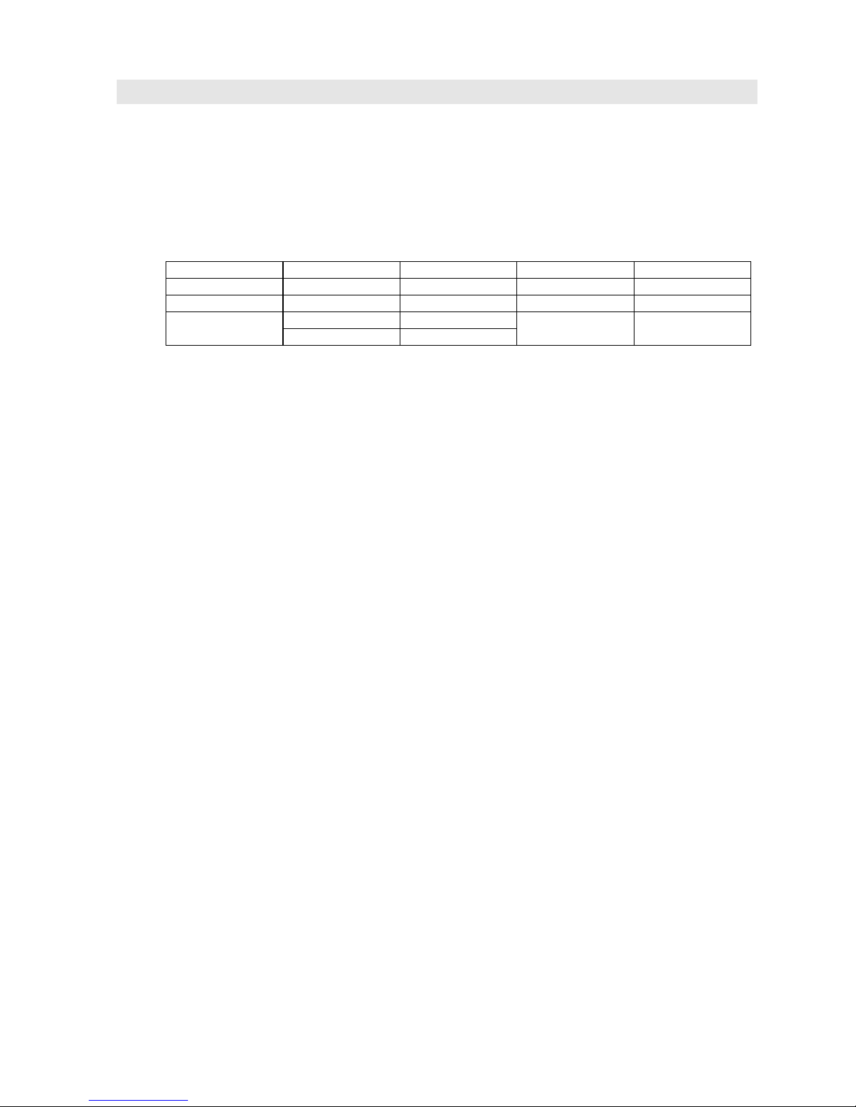
Revision History
Revision Date Description Of Changes Approval
1a 8/28/02 Initial Issue – DCN2564 T. Sears
ii VPW425-1 Service Manual
Page 3
Service Manual
ViewSonic VPW425
Model No. VLCDS22554-1W
42” Plasma TV Monitor
ViewSonic
381 Brea Canyon Road, Walnut, California 91789 USA - (800) 888-8583
(VPW425-1_SM_598 - Rev. 1a – August 2002)
Page 4

Copyright
Copyright
reproduced, transmitted, transcribed, stored in a retrieval system, or translated into any language or
computer language, in any form or by any means, electronic, mechanical, magnetic, optical, chemical,
manual or otherwise, without the prior written permission of ViewSonic Corporation.
Disclaimer
ViewSonic makes no representations or warranties, either expressed or implied, with respect to the
contents hereof and specifically disclaims any warranty of merchantability or fitness for any particular
purpose. Further, ViewSonic reserves the right to revise this publication and to make changes from time
to time in the contents hereof without obligation of ViewSonic to notify any person of such revision or
changes.
Trademarks
ViewSonic is a registered trademark of ViewSonic Corporation.
2002 by ViewSonic Corporation. All rights reserved. No part of this publication may be
All other trademarks used within this document are the property of their respective owners.
Revision History
Revision Date Description Of Changes Approval
1a 8/28/02 Initial Issue – DCN2564 T. Sears
ii VPW425-1 Service Manual
Page 5

TABLE OF CONTENTS
1. WARNINGS & CAUTIONS ................................................................................................................. 1-1
2. SPECIFICATIONS ................................................................................................................................ 2-1
3. EXPLODED VIEW................................................................................................................................ 3-1
4. FACTORY & ELECTRONIC ADJUSTMENTS ................................................................................. 4-1
5. BLOCK DIAGRAM .............................................................................................................................. 5-1
6. TROUBLESHOOTING FLOW CHART .............................................................................................. 6-1
7. PC BOARD ASSEMBLY VIEWS ........................................................................................................ 7-1
8. MAJOR ELECTRONIC ASSEMBLY PARTS LIST............................................................................ 8-1
9. PACKING LIST..................................................................................................................................... 9-1
iii VPW425-1 Service Manual
Page 6
IMPORTANT SAFETY PRECAUTIONS VER1.0
1-01
1. Before returning an instrument to the customer,
always make a safety check of the entire instrument,
including, but not limited to, the follo wing items.
a.
Be sure that no built-in protective devices are defective and/or have been defeated during servicing. (1) Protective
shields are provided on this chassis to protect both the technician and the customer. Correctly replace all missing
protective shields, including any removed for servicing convenience. (2) When reinstalling the chassis and/or
other assembly in the cabine t, be sure to put back in place all pro tective devices, including, but not limited to,
nonmetallic control knobs, insulating fishpapers, adjustment and compartment covers/shields, and isolation
resistor/capacitor networks.
Do not operate this instrument or permit it to be operated without all protective
devices correctly installed and functioning.
b.
Be sure that there are no cabin et openings through which an adult or child m ight be able to i nsert their fingers
and contact a hazard ous volt age, S uch opening includ e, but are not limited to, (1) sp acing bet ween the pictur e
tube and the cabinet m ask, (2) excessively wide cabinet ventilation slots, and (3) an im properly fitted and/or
incorrectly secu red cabinet back cover.
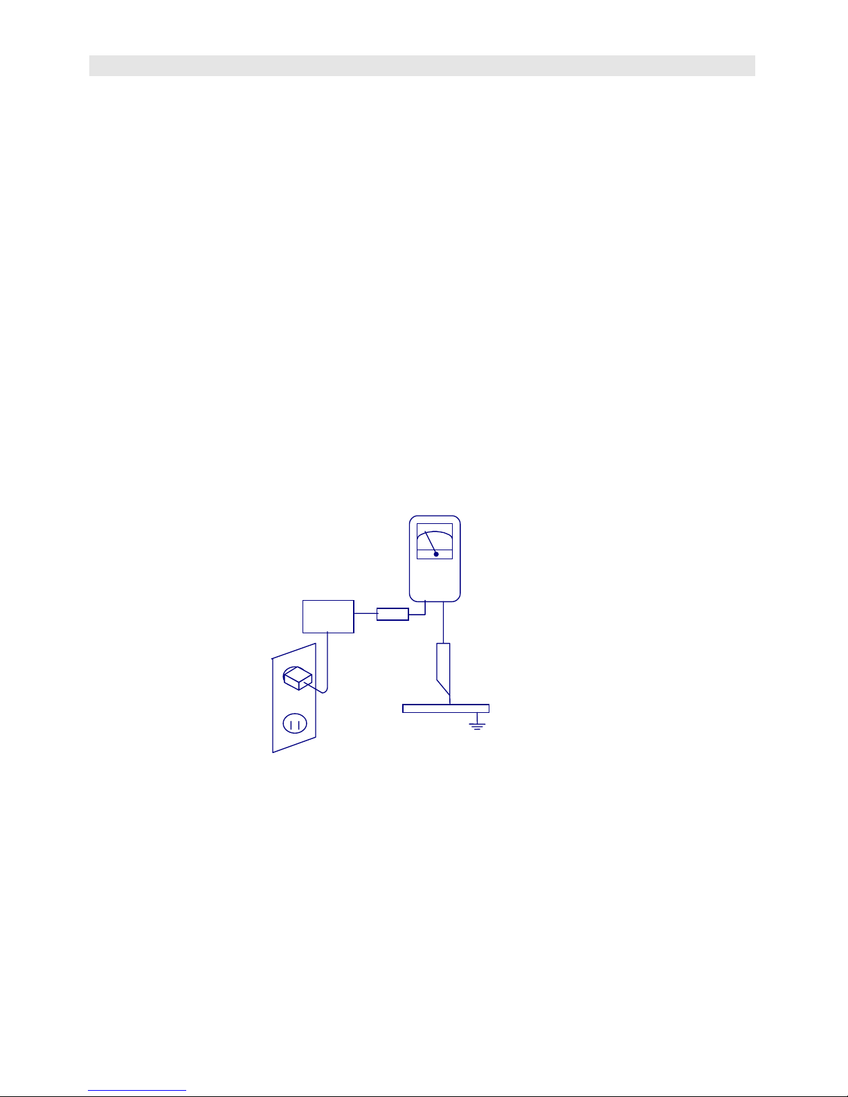
c. Leakage Current Hot Check
—
——
—With the instrument completely reassembled, plug th e A C lin e c ord directly into a
120V AC outlet. (Do not use an isolation tr ans f orm er dur ing this t e st.) Us e a le akage current tester or a metering
system that complies with American National Standards Institutes (ANSI) C101.1 Leakage Current for Appliances
and Underwriters Labor atories (UL) 478. W ith the instrum ent AC switch firs t in the ON position a nd then in the
OFF position, measur e fr om a k nown earth gr ound (m etal wa terpipe, c onduit, etc.) to all ex posed metal par ts of
the instrument (antennas, handle bracket, metal cabinet, screwheads, metallic overlays, control shafts, etc.),
especially any exposed metal parts that offer an electrical return path to the c h as s is. An y curr en t m eas ured must
not exceed 3.5 milliamp. Reverse the instrument power cord plug in the outlet and repeat test.
ANY
MEASUREMENTS NOT WITHIN THE LIMITS SPECIFIED HEREIN INDICATE A POTENTIAL SHOCK
HAZARD THAT MUST BE ELIMINATED BEFORE RETURNING THE INSTRUMENT TO THE CUSTOMER.
2.
Read and comply with all caution and safety-relat ed notes on or inside the Monitor cabinet, on th e Projection
Monitor chassis, or on the picture tube.
3. Design Alteration Warning
—
——
—Do not alter or add to the mechanical or electrical design of this unit. Design
alterations and additio ns, including, bu t not limited to, circuit modific ations and the addi tion of the item s such as
auxiliary audio and/or video output connections m ight alter the safety characteristic s of this Projection Monitor
and create a hazard to the user. Any design alterations or add iti ons will void the manufacturer’s warra nty and wil l
make you, the service, responsible for personal injury or property damage resulting therefrom.
DEVICE
UNDER
TEST
A
LSO TEST WITH
PLUG REVERSED
(USING AC ADAPTER
PLUG AS REQUIRED)
TEST ALL
EXPOSED METAL
SURFACES
LEAKAGE
CURRENT
TESTER
+-
EARTH
GROUND
3. WIRE CORD
A
C Leakage Test
(READING
SHOULD NOR
BE ABOVE
3.5mA)
Page 7

IMPORTANT SAFETY PRECAUTIONS VER1.0
1-02
4. Hot Chassis Warning
————
a.
Some Monitor chassis are electrical ly connected dir ectly to one c onductor of the AC
power cord and may be safely serv iced without an is olation transf ormer only if the AC po wer plug is inserte d so
that the chassis is connected to the gr ound side of the AC power sourc e. To confirm that the AC power plug is
inserted correctly, with an AC voltmeter meas ure between the chassis and a known earth ground. If a voltage
reading in excess of 1.0V is obtained, rem ove and reinsert the AC power plug in opposite pol arity and again
measure the voltage potential between the chassis and a known earth ground. b. Some Monitor chassis normally
have 85V AC (RMS.), between chass is and earth gr ound regar dless of the AC plug polar ity. These chassis can
be safely serviced o nly with an isol ation trans form er insert ed in the p ower lin e bet ween the r eceiver and the AC
power source, for both personnel and test equipment protec tion.
c.
Some Projection Monitor chassis have a
secondary ground systems in addition to the main chassis ground. T his s ec ond ar y gr oun d system is not isol ated
from the AC power line. The two ground system ar e elec tric a ll y sep arated by insulating material that must not be
defeated or altered.
5.
Observe original le ad dress. Take extra care to assure correct l ead dress in the following are as:
a.
near sharp
edges, b. near thermally hot par ts—b e sure that le ads a nd com ponents do not t ouch ther m ally hot par ts,
c.
the
AC supply,
d.
high voltage,
e.
antenna wiring. Alwa ys inspect in all areas for pinched , out-of-place, or frayed
wiring. Do not change spacing between components, and betwe en components and the printed-c ircuit board.
Check AC power cord for damage.
6.
Components, parts, and/or wiring that appear to have overheated or are otherwise damaged should be replaced
with components, parts, or wireing that meet original specifications. Additionally, determine the cause of
overheating and/or damage and, if necessary, take corrective action to remove any potential safety hazard.
7. PRODUCT SAFETY NOTICE
—
——
—Many Monitor electrical and mechanical parts have special safety-related
characteristics some of which are often not evident from visual inspection, nor can the protection they give
necessarily be obtained by replacing them with components rated for higher voltage, wattage, etc. Parts that have
special safety charac teris tics ar e ide ntifie d in th is s ervic e data by shad ing with a mark on schem atics and by
shading or a * mark in the parts lis t. Use of a s ubstitute rep lacement part t hat does not hav e the sam e safety
characteristics as the recommended replacement part in this service data parts list might create shock, fire,
and/or other hazards.
Page 8

SPECIFICATION VER1.0
2-1
1. SCOPE:
These specifications describe all the characteristics of the 42 inch color monitor .
2. ELECTRICAL REQUIREMENTS:
2.1. Display panel: Specification
a. Screen size Diagonal 42 inch
b. Aspect ratio 16:9 wide
c. Number of pixels 852(Horizontal, RGB Trio ) X 480(Vertical)pixels
d. Pixel Pitch 1.08mm X 1.08mm
e. Luminance 570cd/m
2
,at APL13%
f. Chromatically
x=0.270
±±±±
0.03, y=0.300
±±±±
0.03(color temperature mode 1 : ) at
center block white pattern 100% (mosaic).
2.2. Power Source:
a. Input voltage 100 ~ 240 Vac , 50 / 60 Hz
b. Input current 3.3A
c. Inrush current 60 A p-p/20ms Max.
d. Power consumption
380
±±±±
10% Watts ( at 110V ac/color bar pattern)
e. Stand-by & DPMS 5 Watts Max. (at 110Vac)
2.3. Input Signal:
2.3.1 Connector Type:
RCA Jack for audio, video Y/C
B/CR
and Y/PB/P
R
6 pin Din S-terminal
9 pin D-SUB
15 pin D-SUB
24 pin DVI
2.3.2 Video/S-Video Signal:
a. Type Analog
b. Polarity Positive
c. Amplitude
d. Frequency
Video 1Vp-p , (priority S-Video) Y=1Vp-p C=0.286Vp-p
H: 15.734KHz V: 60Hz(NTSC)
H: 15.625KHz V: 50Hz(PAL)
e. Input impedance 75 ohms
2.3.3 Y/CB/CR or Y/PB/PR Signal:
a. Type Analog
b. Polarity Positive
c. Amplitude AV: 1Vp-p (with sync)
S-Video: Y: 1Vp-p ,C: 0.286Vp-p
d. Frequency
Y/CB/C
R
Y/PB/PR: HDTV
H: 15.734KHz ,V: 60Hz (NTSC)
H: 15.625KHz ,V: 50Hz (PAL)
1. 31KHz/60Hz (480P)
2. 45KHz/60Hz (720P)
3. 33KHz/60Hz(1080I)
Page 9

SPECIFICATION VER1.0
2-2
2.3.4 RGB Signal:
a. Type
TTL
b. Polarity
Positive or Negative
c. Amplitude RGB: 0.7Vp-p
d. Frequency H: support to 31K~91KHz
V: support to 50~85Hz
2.3.5 DVI Signal:
a. Type
b. Polarity
c. Frequency
Digital
Positive or Negative
H: support to 31K~63KHz
V: support to 50~85Hz
2.3.6 Audio Signal: Analog 500mV rms /more than 22Kohm
2.3.7 Pin Assignments For D-SUB Connector (In / Loop Out):
Pin Signal Assignment Pin Signal Assignment Pin Signal Assignment
1 RED 6 RED GND 11 GND
2 GREEN 7 GREEN GND 12 SDA
3 BLUE 8 BLUE GND 13 H-SYNC
4GND 9NC 14V-SYNC
5 GND 10 GND 15 SCL
2.3.8 Pin Assignments For 24 Pin DVI Connector(Digital Only):
Pin Signal Assignment Pin Signal Assignment Pin Signal Assignment
1 TMDS Data 2- 9 TMDS Data 1- 17 TMDS Data 02 TMDS Data 2+ 10 TMDS Data 1+ 18 TMDS Data 0+
3 TMDS Data 2/4 Shield 11 TMDS Data 1/3 Shield 19 TMDS Data 0/5 Shield
4 TMDS Data 4- 12 TMDS Data 3- 20 TMDS Data 55 TMDS Data 4+ 13 TMDS Data 3+ 21 TMDS Data 5+
6 DDC Clock 14 +5V Power 22 TMDS Clock Shield
7 DDC Data 15 Ground (For +5V) 23 TMDS Clock +
8 No Connect 16 Hot Plug Detect 24 TMDS Clock -
Page 10
SPECIFICATION VER1.0
2-3
2.3.9 RGB/DVI For VESA Standard:
Mode No Resolution
Refresh
Rate
Horizontal
Frequency
Vertical
Frequency
Vertical
Sync
Polarity
Horizontal
Sync
Polarity
Dot rate
(Hz) (K Hz) (Hz) (TTL) (TTL) (MHz)
1
640(VGA)
××××
480
60 31.5 59.94 - - 25.175
2
640(VGA)
××××
480
72 37.9 72.81 - - 31.500
3
640(VGA)
××××
480
75 37.5 75 - - 31.500
4
640(VGA)
××××
480
85 43.3 85.01 - - 36.000
5
800(SVGA)
××××
600
56 35.1 56.25 + + 36.000
6
800(SVGA)
××××
600
60 37.9 60.317 + + 40.000
7
800(SVGA)
××××
600
72 48.1 72.19 + + 50.000
8
800(SVGA)
××××
600
75 46.9 75 + + 49.500
9
800(SVGA)
××××
600
85 53.7 85.06 + + 56.250
10
1024(XGA)
××××
768
60 48.4 60.01 - - 65.000
11
1024(XGA)
××××
768
70 56.5 70.07 - - 75.000
12
1024(XGA)
××××
768
75 60.0 75.03 + + 78.750
13
1024(XGA)
××××
768
85 68.7 84.99 + + 94.500
14
1280(SXGA)
××××
1024
60 63.98 60.02 + + 108.00
15
◎◎◎◎
1280(SXGA)
××××
1024
75 79.98 75.03 + + 135.00
16
◎◎◎◎
1280(SXGA)
××××
1024
85 91.15 85.02 + + 157.50
18
640(VGA)
××××
350
70 31.50 70 - - 25.175
19
640(VGA)
××××
480
50 31.5 50 - - 25.175
20
◎◎◎◎
1280(HDTV)
××××
720P
60 45.15 60 - - 74.250
21
◎◎◎◎
1920(HDTV)
××××
1080I
60(I) 33.78 60 - - 74.250
22
720(DOS)
××××
400
70 31.46 70.08 + - 28.320
23
852(WGA)
××××
480
60 31.72 60.41 - - 34.00
RGB/DVI For Apple Standard.
Mode No Resolution
Refresh
Rate
Horizontal
Frequency
Vertical
Frequency
Vertical
Sync
Polarity
Horizontal
Sync
Polarity
Dot rate
(Hz) (K Hz) (Hz) (TTL) (TTL) (MHz)
24
640
××××
870
75 68.85 75.00 - - 57.283
25 832 x 624 75 49.73 74.55 - - 57.283
26 1152 x 870 75 68.68 75.06 - - 100.000
Attention
◎◎◎◎
: For DVI is not supported.
2.3.10 Y/PB/PR For Component:
Mode No Resolution Refresh Rate
1
640
××××
480P
60
2
1920
××××
1080I
60
3
1280
××××
720P
60
Page 11

SPECIFICATION VER1.0
2-4
2.4. Display Performance Requirements:
The data of display performance are measured based on the following.
Conditions unless otherwise specified.
a. Ambient temperature
25
±±±±
5
℃℃℃℃
b. Warm up period 30 minutes Min.
c. Line input voltage : 100 Vac ~ 240 Vac (50 / 60 Hz)
d. Viewing distance Distance from screen is 81 cm
e. Display mode Test with window white pattern mode if not specified.
f. Brightness condition Press recall bottom to set default brightness
2.4.1 Maximum Resolution: Support to 1280 x 1024
2.4.2 Horizontal Size (Standard) 920
±±±±
8 mm (for mode 1
〜〜〜〜
26)
Vertical Size (Standard) 518
±±±±
8 mm (for mode 1
〜〜〜〜
26)
2.4.3 Horizontal Size (Max.) Mode 1~26
ÖÖÖÖ
full-scan
Vertical Size (Max.) Mode 1~26
ÖÖÖÖ
full-scan
2.4.4 Maximum Brightness Level: Timing Mode 1
a. 100% center block white
pattern(mosaic)
More than 30FL
(while pressing recall button to set default brightness)
b. raster background with contrast / brightness at Max. and black signal)
less than 0.4FL
2.5. Operation:
Main unit button
Main power switch (power ON /OFF)
Power ON/OFF
Input Mode (Video1 -> S-Video1 -> Video2 or S-Video2 ->
Y/P
B/PR
1 or Y/CB/CR 1 -> Y/PB/PR 1 or Y/CB/CR 1 -> RGB ->
DVI->Video1 run in circle)
Menu key -,+ Adjustment -,+
IR Remote Control Power on/off
Input Mode (same as Main unit button)
Volume -,+ Wide , Video/S video
input:4:3/16:9/ZOOM1/ZOOM2
Analog RGB input :W4:3/W16:9
Menu -,+ Adjustment -,+ RECALL
PIP ,POP ,SWAP ,MUTE
2.5.1 Adjustable Items:
AV/S-video input Brightness, Contrast, Color , Tint, Sharpness
Y/CB/CR Color Temperature
Analog RGB input
DVI input
Display position :
Brightness, Contrast, Vertical position, Vertical width,
Horizontal position, Horizontal width, Color Temperature
Clock phase, DPMS.
Brightness, Contrast, Vertical position, Vertical width,
Horizontal position, Horizontal width, Color Temperature,
DPMS
3. DIMENSIONS: Without/Stand With/Stand
Page 12

SPECIFICATION VER1.0
2-5
Width
Height
Depth
1040mm
648 mm
95mm
1040mm
690mm
375 mm
3.1. Package Dimensions:
Width 1230 mm
Height 960 mm
Depth 470 mm
3.2. Weight:
Net weight 79.4lbs/36 Kgs (w/o stand) 83.8lbs/ 38Kgs (w/ stand)
Gross weight 115lbs/52 Kgs
4. ENVIRONMENT:
4.1. Operating:
Temperature
0~40
℃℃℃℃
(32~104
℉℉℉℉
)
Relative humidity 20~80%
Pressure 800~1114hpa
4.2. Non-Operating:
Temperature
-20~60
℃℃℃℃
Relative humidity 20~90%
Pressure 700~1114hpa
Vibration X/Y/Z, 0.5G/10~55Hz(sweep), 10 minutes
4.3. Acoustics:
(IHF A-weighted 1meter) 40dB Max.
5. SOUND:
a. Residual hum (at volume min)
500
μμμμ
W Max.
b. Practical max. Audio output (at 10% THD max.)
1.0vp-p 1K Hz input 5W +5W Max. /12 ohm
c. Sound distortion (at 250 mw 1K Hz)
d. Sound distortion (at
i.ovp-p 1kHz input volume max )
1% Max.
9% max
e. Audio output (input at 1.4V
P-P
)
≧≧≧≧
1.0 V
P-P
f. Max. hum (at volume max)
1000
μμμμ
W Max.
g. Sensitivity (at volume max. O/P 1W)
at 1KHz AV Input
150mV
±±±±
3dB
h. Audio Fidelity (1KHz 0dB,corrected for emphasis characteristics)
BBE ON 60Hz
6dB
±±±±
3dB
10KHz
8dB
±±±±
3dB
WOOFER & BBE OFF 100Hz
-6dB
±±±±
3dB
10KHz
-2dB
±±±±
3dB
6. RF
Page 13

SPECIFICATION VER1.0
2-6
6.1 RF Sensitivity (Peak)
VHF CH 2 ~ CH 13 30dB Max.
UHF CH 14 ~ CH 69 30dB Max.
CATV CH A-5 ~ CH W+29 30dB Max.
6.2 AFT Pull-In Range
VHF CH 2 ~ CH 13
±±±±
0.6MHz Min.
UHF CH 14 ~ CH 69
±±±±
0.6MHz Min.
CATV CH A-5 ~ CH W+29
±±±±
0.6MHz Min.
6.3 Picture IF Rejection
VHF CH 2 ~ CH 13 50dB Min.
UHF CH 14 ~ CH 69 50dB Min.
CATV CH A-5 ~ CH W+29 50dB Min.
6.4 Picture Image Rejection
VHF CH 2 ~ CH 13 40dB Min.
UHF CH 14 ~ CH 69 35dB Min.
CATV CH A-5 ~ CH W+29 35dB Min.
6.5 AGC Characteristics
AGC Figure Of Merit 50dB Min.
RF signal range in which video at PDP drops 6 dB from output level obtained
with 100mV input.
6.6 RF AGC Cut In Level
55dB
±±±±
2dB
6.7 FM/AM Rejection (100mV at SIF input) 14dB min
6.8 Noise Limits Sensitivity VHF 45dB max
UHF 49dB max
7. RELIABILITY REQUIREMENT:
The MTBF needs 20000hrs under operation 25
±±±±
5
℃℃℃℃
(half luminosity, motion picture)
8. REGULATORY REQUIREMENTS:
8.1 Safety Requirement:
a. UL Safety of information technology equipment including
electrical business equipment
b. CSA Safety of information technology equipment including
electrical business equipment
c. TUV
8.2 Emission Requirement:
The unit shall meet the EMI limits in all screen modes. For EMI testing, the unit must be failed
with the screen pattern consisting of scrolling capital “H” characters also the brightness
contrast will be adjusted to max. Level.
a. FCC class A part 15
8.3 Transit test
Page 14
SPECIFICATION VER1.0
2-7
a. Drop Test 200mm max.
b. Vibration Test
1. Forward and backward
2. Right and left
3. Up and down
30 minutes 1000 c.p.m
30 minutes 1000 c.p.m
30 minutes 1000 c.p.m
8.4 Power Management:
Mode H-sync V-sync Video Power dissipation
Normal Pulse Pulse Active Normal power
Stand-by No pulse No pulse No video Power off
Pulse No pulsePower saving
No pulse Pulse
Blanked Less than 5 watts
This Plasma display is Energy star compliant when used with a computer equipped with
DPMS.
Note: The power indicator LED color is green in normal state, yellow in stand-by
and power saving state.
9. VIDEO & AUDIO
9.1 Video Signal Output (impedance 75 ohm)
(input signal at 1.0 Vp-p
±±±±
0.2Vp-p)
1.0 Vp-p
±±±±
0.2Vp-p
Page 15
SPECIFICATION VER1.0
2-8
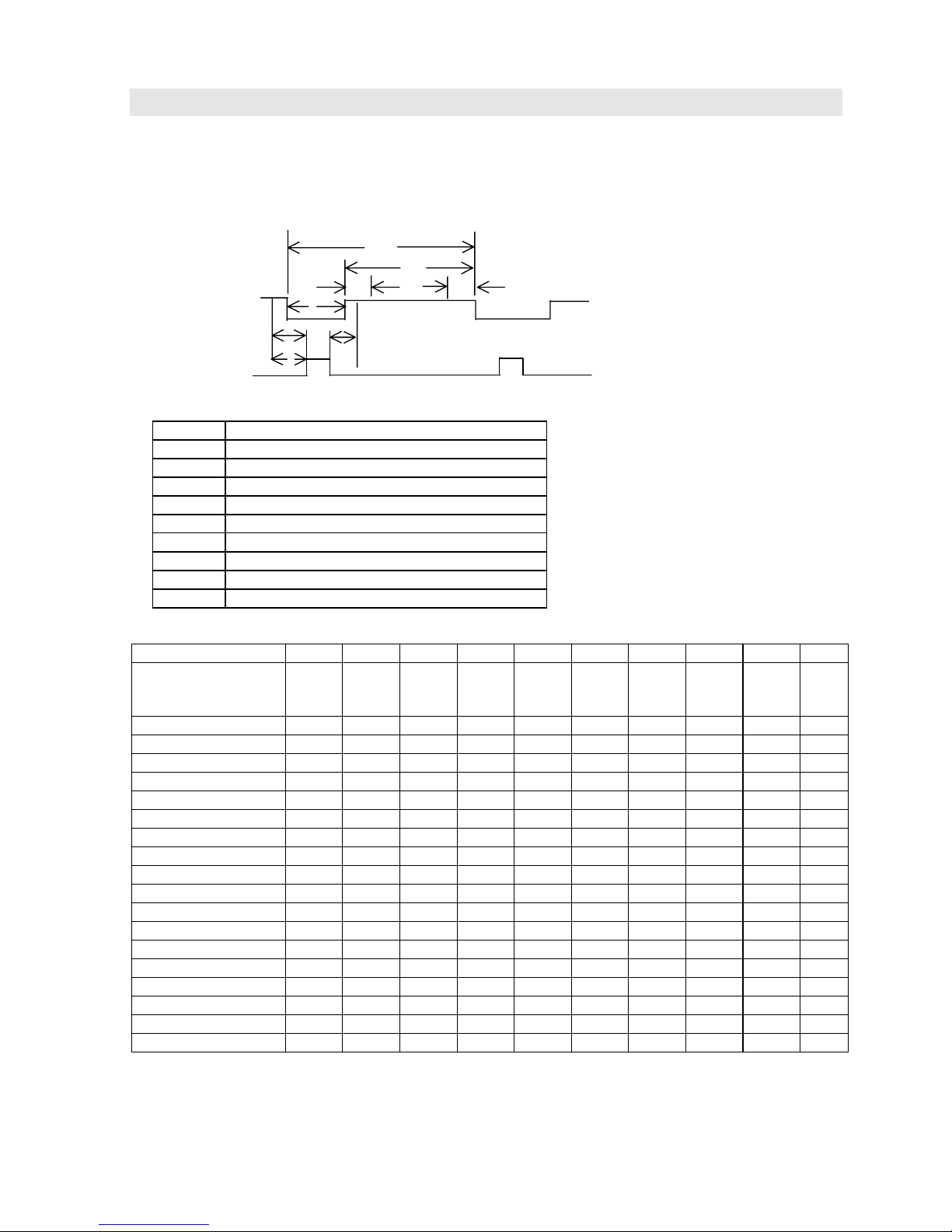
APPENDIX A :
Preset Timing Ch art
Item Description:
A Total time
B Active display area including borders
C Active display area excluding borders
D Left/Top border
E Right/bottom border
F Blanking time
G Front porch
HSync-width
I Back porch
Mode No 123456789
Resolution
&
Refresh Rate
640
480
60
640
480
72
640
480
75
640
480
85
800
600
56
800
600
60
800
600
72
800
600
75
800
600
85 Hz
Pixel 25.175 31.5 31.5 36 36 40 50 49.5 56.25 MHz
Horizontal visible 640 640 640 640 800 800 800 800 800 Dots
Horizontal total 800 832 840 832 1024 1056 1040 1056 1048 Dots
Horizontal front porch 24 32 16 56 24 40 56 16 32 Dots
Horizontal sync 96 40 64 56 72 128 120 80 64 Dots
Horizontal back porch 40 120 120 80 128 88 64 160 152 Dots
Horiz blanking time 160 192 200 192 224 256 240 256 248 Dots
Vertical visible 480 480 480 480 600 600 600 600 600 Lines
Vertical total 525 520 500 509 625 628 666 625 631 Lines
Vertical front porch 181711113711Lines
Vertical sync 233324633Lines
Vertical back porch 25 20 16 25 22 23 23 21 27 Lines
Vertical blanking time 45 40 20 29 25 28 66 25 31 Lines
Horizontal frequency 31.469 37.9 37.5 43.3 35.1 37.9 48.1 46.9 53.7 KHz
Vertical frequency 59.94 72.81 75 85.01 56.25 60.317 72.19 75 85.06 Hz
Vertical sync polarity- - - -+++++TTL
Horiz sync polarity - - - -+++++TTL
Dot rate 25.175 31.5 31.5 36 36 40 50 49.5 56.25 MHz
A
B
C
E
D
H
F
I
G
(Video)
(Sync)
Page 16

SPECIFICATION(Preliminary)
2-9
Mode No 10 11 12 13 14 15 16 18 19
Resolution
&
Refresh Rate
1024
768
60
1024
768
70
1024
768
75
1024
768
85
1280
1024
60
1280
1024
75
1280
1024
85
640
350
70
640
480
50 Hz
Pixel 65 75 78.75 94.5 108 135 157.5 25.175 25.175 MHz
Horizontal visible 1024 1024 1024 1024 1280 1280 1280 640 640 Dots
Horizontal total 1344 1328 1312 1376 1688 1688 1728 800 800 Dots
Horizontal front porch 24 24 16 48 48 16 64 16 16 Dots
Horizontal sync 136 136 96 96 112 144 160 96 96 Dots
Horizontal back porch 160 144 176 208 248 248 224 48 48 Dots
Horiz blanking time 320 304 288 352 408 408 448 160 160 Dots
Vertical visible 768 768 768 768 1024 1024 1024 350 480 Lines
Vertical total 806 806 800 808 1066 1066 1072 449 629 Lines
Vertical front porch 33111113762Lines
Vertical sync 663333322Lines
Vertical back porch 29 29 28 36 38 38 44 60 85 Lines
Vertical blanking time 38 38 32 40 42 42 48 99 149 Lines
Horizontal frequency 48.4 56.5 60 68.7 63.98 79.98 91.15 31.50 31.5 KHz
Vertical frequency 60.01 70.07 75.03 84.99 60.02 75.03 85.02 70 50 Hz
Vertical sync polarity- -+++++- -TTL
Horiz sync polarity - -+++++- -TTL
Dot rate 65 75 78.75 94.5 108 135 157.5 25.175 25.175 MHz
Mode No 20 21 22 23 24 25 26
Resolution
&
Refresh Rate
1280
720P
60
1920
1080I
60I
720
400
70
852
480
60
640
870
75
832
624
75
1 152
870
75 Hz
Pixel 74.250 74.25 28.320 30 57.283 57.283 100.000 MHz
Horizontal visible 1266 1901 720 852 640 832 1152 Dots
Horizontal total 1650 2201 900 955 832 1152 1456 Dots
Horizontal front porch 42 68 18 19 32 32 32 Dots
Horizontal sync 63 63 108 48 80 64 128 Dots
Horizontal back porch 279 169 54 36 80 224 144 Dots
Horiz blanking time 384 300 180 103 192 320 304 Dots
Vertical visible 687 518 400 480 870 624 870 Lines
Vertical total 750 562.5 449 525 918 667 915 Lines
Vertical front porch 1 0.5 12 10 3 1 3 Lines
Vertical sync 6622333 Lines
Vertical back porch 56 38 35 33 42 39 39 Lines
Vertical blanking time 63 44.5 49 45 48 43 45 Lines
Horizontal frequency 45.15 33.78 31.46 31.72 68.85 49.73 68.68 KHz
Vertical frequency 60 60 70.08 60.41 75.00 74.55 75.06 Hz
Vertical sync polarity - - + - - - - TTL
Horiz sync polarity - - - - - - - TTL
Dot rate 74.25 74.25 28.32 30 57.283 57.283 100.000 MHz
Page 17

EXPLODED VIEW VER1.0
3-1
Page 18

FACTORY ADJUSTMENT METHOD VER1.0
4-1
DIGITAL BOARD
CN01
EXT INT
CN05
EXT INT
CN01 SELECT "INT"
CN05 SELECT "EXT"
1. PANEL voltage adjustment
The power voltage should be adjusted and checked when changing the panel or power board.
POWER VOLTAGE ADJUST FOR SAMSUNG TTL PANEL
GND
1. DIGITAL BOARD CON01 SELECT TO "INT".
2. DIGITAL BOARD CON05 SELECT TO "EXT".
3. MAKE A SW CONNECT TO POWER BOARD CON80011 PIN 1 & PIN5 FOR POWER
SWITCH.
4. FOLLOW THE PANEL LABEL VOLTAGE ADJUST VR.
5. VOLTAGE CHECK FROM "CHECK POINT" WITH GRAND.
6. ADJUST SEQUENCE
1st → 2nd → 3rd → 4th → 5
th
VA VSC VS VR VSET
VR8005 VR8006 VR8003 VR8001 VR8007
VA VSC VS VR VSET
PIN 1 & 5 CONNECT A POWER SWITCH
VOLTAGE CHECK POINT
POWER BOARD
Page 19

FACTORY ADJUSTMENT METHOD VER1.0
4-2
2. Color temperature adjustment
Push the factory service key to into the adjustment mode. The following will appear:
DVI
5400ºk
X=0.335 Y=0.343
GAIN Bias
RGB RGB
XXX XXX
Use the AV key to select the color to adjust andorkey to adjust the level.
The required equipment is CA-100,Vp300.
a. Adjust Bias first to set Y to 0.4 on CA-100. Adjust R or B to set the value of X,Y
on CA-100 to be the same as the value showing screen, The value of Y should be
maintained at 0.4 during adjustment.
b. Move the cursor to adjust Gain. The value of Y should be adjusted to 25. Then
adjust R or B to let the value of X,Y on CA-100 be the same as the value showing
on screen. The value of Y should be maintain 25 during the adjustment.
c. Repeat to check the Bias an d Gain. The v alue o f Y,X and Y sh ould be the same as
the previous adjusted value. Then the DVI 5400ºk mode is adjusted complelely.
d. Push the factory service key again to next pi cture. Then repeat the steps a. b. c. to
adjust.
e. If the adjustment is completed, sepeat d. a. b. and c steps to adjust again.
f. When the last mode AV 13000ºk is adjusted completely, push the factory service
key again to leave the adjustment mode,
Note: 1. There are 12 adjusted modes(DVIx4.RGBx4 AVx4)
2. The adjusted sequence is DVIRGBAV.
3. DVI/RGB : Bias Y=0.4
Gain Y=25
AV : Bias Y=1
Gain Y=25
Page 20

BLOCK DIAGRAM VER1.0
5-1
J25_1
Pin[1:3]
PANEL Power
Supply Ass'y
AC IN_1
7
AV Module
Board(with
Tuner)
Assy
9
J12_1
Pin[1:10]
1
SA_1
CON8011
Pin[1:6]
Pin[7:13]
LA03_1
Pin[1:31]
5
3
JA3_1
Pin[1:6]
12
2
JA1_1
Pin[1:12]
Logic F-Buffer
AC OUT_1
13
J1_1
Pin[1:31]
Logic Board Ass'y
(5V , S B D E T )
(Audio DC,Supply)
AUDIO_1
CON8009
Pin[1:2]
Pin[1:7]
(LVDS)
JA2_1
Pin[1:10]
JP2_1
Pin[1:32]
J11_1
Pin[1:12]
JP5_1
Pin[1:48]
Y Amp Board-Upper
Audio Amplifier
Board Ass'y
(9V )
J14_1
Pin[1:6]
(24V,9V)
(5V )
10
Image Boa rd
Ass'y
Interface Board- Z Ass'y
J15_1
Pin[1:4]
11Logic E-Buffer
J5_1
Pin[1:6]
PDP Socket Diagram
Front
Button
Control
Board
Assy
Y Amp Board-Lower
AC Master power swith Bo ar d
SAMPO Board Assembly
(Audio Signal)
SW_1
14
Power
SW
Interface Board- Y Ass'y
JP4_1
PinA[1:48]
4
6
Panel's Board Assembly
AC
PLUG
JP1_1
Pin[1:32]
Power Input
Module
Assy
8
J21_1
Pin[1:7]
(Ke y)
Page 21

BLOCK DIAGRAM VER1.0
5-2
A9
GND
A8
NC
Pin 1
A5
A14
B3
A16
GND
A3
A10
A6
RD-
YUV2_R
Pin 8
P5V
C2
DVI_L
B12
PWR_CTL
SDA2
R_IN
15Kn_SP
VGNDNC
C10
Pin 1
NC
Pin 6Pin 7
AGND
Pin 40
C13
GND
B12
Pin 1
AFT_TUN
B4
C12
B5
A10
B14
C6
Pin 35
DGND
Pin 1
GND
DGND
DGND
B13
SURR1
NC
Pin 3 J5 (6 Pin)
RST _ DP T V
A2
C11
SV2_SW
GND
AO_SEL
B4
C4
Pin 5
YUV1_R
Pin 21
AGND
Pin 15
B1
Pin 6
C1
RGB_ R
+5VSB
B16
B2
C9
Pin 16
Y1
Pin 4
GND
Pin 1
TCK
AGND
GND
GND
A13
C12
A6
A10
B2
Pin 2
SB
D_CT L
PR2_CR2
Pin 4
NC
GND
Pin 9
S2_Y
B8
Image Board ←→ Panel
AGND
C14
B11
R_OUT
C13
NC
Pin 11
RA-
J11 (12 Pin)
C6
A5
5V1
C5
RB+
NC
A6
B1
C9
A16
J14 (6 P i n )
C5
AGND
DGND
SDA2
C16
GND
Pin 19
DGND
NC
C1
A9
Image Board
S2_L
A3
Pin 9
Pin 12
A9
B11
A11
DGNDPin 12
B15
B7
C11
J15 (4 P i n )
GND
RC-
B16
A15
Image Board ←→ Audi o Amplifier Boar d
B1
L_IN
A10
JP5 (48 Pin)
YUVn_RGB
B16
C8
AGND
Pin 39
Pin 5
Audio A mplifier Board
RC+
PCSI
AV Module Board
SCL_SP
A1
Pin 8
DGND
C1
A2
SPK_CTL
C9
SDA2
A15
B15
TDI
A7
Pin 7
Pin 38
GND
VGND
B9
GND
Image Board Ass'y
NC
TUN_DETn
AS_MP
VGND
B3
PCn_MPU
Pin 23
Pin 10
L_OUT
Pin 3
Pin 24
A7
PB1_CB1
B10
Pin 10
V2B_DETn
A16
A8
+5VA
A11
Pin 4
A14
C2
A5
Image Board
DGND
B3
Pin 10
Pin 36
Pin 7
GND
JA1 (12 Pin)
JP2 (48 Pin)
A8
GND
C11
Audio A mplifier Board
+9VT
C12
C16
B1
NC
AV1_R
B5
Pin 2
Pin 2
Pin 11
A3
C2
+24V
SURR2
C3
AGND
C7
RGB_ L
PB2_CB2
JP2 (48 Pin)
B14
B8 B9
Pin 8
Pin 28
Pin 2
Pin 1
GND
C7
C14
DGND
RCLK-
TMS
NC
Pin 9
AGND
A7
A14
SCL2
NC
Pin 5
SSO
R_OUT
C11
Pin 6
C3
B6
AGND
Pin 25
Pin 7
NC
B11
GND
TV
JA3 (6 P i n)
B13
A9
C5
B4
Pin 17
Pin 9 PWR_CTL
C6
A6
AS_SP
A13
Pin 31
Content
A14
B9
A11
B13
B9
DGND
SB5V
C2
B7
NC
J12 (10 Pin)
NC
A1
A_MUTEn
A16
VGND
Pin 13
C4
B10
A7
S2_C
Pin 6
A4
C1
A12
B15
RC_OUT
Pin 10
Pin 3
B12
A4
B5
+9V
Pin 33
AGND
NC
Content
A13
C15
DGND
A4
RESE T Q
NC
A12
J1 (40 P in)
B13
Pin 30
Pin 6
RCLK+
SB5V
Content
DGND
Pin 5
Pin 12
Pin 4
24V
B2
+9VT
C15
RA+
JP5 (48 Pin)
B14
C8
SCL2 Pin 5
B10
A11
C8
B11
Image Board Socket Data
COM P O S IT E
Pin 37
Content
B15
A4
B14
C15
DGND
Pin 32
C14
C13
DGND
AGND
Pin 29
Pin 4
Image Board ←→ Audio Amplifier Board
PR1_CR1
Pin 1
Pin 3
Pin 3
B7
B8
C5
Image Board ←→ AV Module Boar d
RD+
TV_R
A2
C10
VGND
C7
C10
C8
C9
SDA2_33
Pin 5
A5
B4
C10
DGND
B6
TV_L
B5
Pin 27
J21 (7 P i n )
NC
Pin 22
Pin 2
Image Board ←→ Front Button Control Board
GND
SW_OUT
AVB_DETn
Pin 5
PCSCS
Pin 3
SUB_WFR
C4
Content
C16
AGND
VGND
AV1_L
DGND
C15
SD
B6
Pin 8
PCSCLK
Pin 4
VGND
A1
C3
AGND
AGND
A2
Pin 26
B12
C7
Pin 7
Image Board
Pin 14
Image Board
Image Board
Pin 18
SCL2_33
C3
SCL2
Pin 8
+24V
J25 (3 P i n )
L_OUT
B6
SUB_WFR
Pin 34
DGND
AGND
C6
VGND
DVI_R
NC
S2_R
Pin 2
Pin 10
YUV1_L
A15
C12
TDO
Image Board ←→ AV Module Boar d
SB_LED
24V
A3
C13
Pin 9
DGND
Pin 3
Pin 6
A12
Pin 20
B2
NC
C14
Y2
JA2 (10 Pin)
15Kn_MP
B10
B8
Pin 2
DGND
VGND
RB-
A15
A1
A12
NC
SDA_SP
Front Button Control
Board
Pin 6
YUV2_L
A13
B7
B3
AV Module Board
C16
ON_LED
Pin 11
A8
B16
C4
Pin 4
DGND
SB5V
Page 22

BLOCK DIAGRAM VER1.0
5-3
P
A
N
E
L
C711/C713
Clock
Generator
CPU
(PAGE10)
(PAGE12)
(PAGE7)
(PAGE4)
C
(PAGE8)
SDRAM
(PAGE2)
(PAGE9)
6630/6730
MAIN Video
Processor
Y1/CB/CR
LVDS
TRANSMITTER
U45
6630/6730
SUB Video
Porcessor
SDRAM
U4
IC2
C
SDRAM
(PAGE3)
IC7
YUV
(PAGE6)
U46
MULTIPLEX
SWITCH
RGB IN
Y
VIDEO
Y
YCBCR/YPBPR
VIDEO
SIL161 DVI
MULTIPLEX
SWITCH
U34
(PAGE1)
R,G,B
YCBCR/YPBPR
Y1/PB/PR
AD
Converter
IC1
(PAGE11)
IC3
TA1276
Color Space
Conveter
MULTIPLEX
SWITCH
U32
MULTIPLEX
SWITCH
RGB OUT
RS232
SCALE IC
(PAGE5)
U43
S-VIDEO
U29
(PAGE14)
(PAGE13)
Y2/PB/PR
Image Board Signal Block Diagram
TV
AV
TA8551CH
AV
SWITCH
9161A(PLL)
DVI IN
Y2/CB/CR
U23
YCBCR
Page 23

BLOCK DIAGRAM VER1.0
5-4
U59
(5V_O SD)
V33P
VCCPLL
U62
P5V_COLOR
J25
1
2
3
V25_SP
CON8009
1
2
3
4
5
6
7
8
9
(VCC3_M_S)
VADC3
P9V
J25
1
2
3
VADC3_S
(VDD33)
U52
USB3V
(VDRAM )
L17
P24V
SB5V_V
5VDDD
(VCC3_M)
U58
5VDDM1
REG_5V
+5VA
U28
U61
+9V
SB5V
V33ADC
V33TMP
J14
1
2
3
4
5
6
L13
U57
V33
VDDM
U31
+9VT
A5V
U60
D3
+5VA
(USB5V, SB5V_M, SB5V_IO, SB5V_CPU)
+5VSB
VCCBF
U13
J21
1
2
3
4
5
6
7
V33SB
SB5V_VO
U53
Image board Power Block Diagram
D2
VCC3
U63
U56
J15
1
2
3
4
(+9V)
VCC3_S
P5V
REG_5V_S
V33PLL
U55
V25_MP
IC9
DVI_5V
+24V
CON8011
1
2
3
4
5
6
7
8
9
10
11
12
13
A5V
VIP711
5VDDA
R376
VCCA3
L15
U54
D43
+5V1
VCCA3_S
Page 24

BLOCK DIAGRAM VER1.0
5-5
FROM A V
SELECTOR
IC2
ICR1
MA IN P OWE R
AMPLIFIER
U1
BUFFER
AMPLIFIER
SUB_WOOFER
OUTPUT
INSIDE
SPEAKER
MUTE
ICA3
FIXED/VARIBL E
OUTPUT
SELECTOR
Q8/Q9/Q11
ICS2
AV_ OUTPUT
MUTE
PDP Sound Block Diagram
Q1/Q2
DPWB11372-1G-S-
INPUT BUFFER
LPF
PAGE2
MUTE
ICS1
IC1
ICA1/ICA 2
BBE & SOUND
PROCESSOR
PAGE1
SRS SURROUND
PROCESSOR
Page 25

BLOCK DIAGRAM VER1.0
5-6
TU201 RF MODULE
SCL2
Q241
2SC2482
IC202
7805
IC241
DPWB11372-1G-T-
9V
POWER BLOCK
AUDIO OUT
NE55 5
IC203
9V_T
JP2
31V
UPC 1854ACT
IC201
VIDEO OUT
MTS
TV_R OUT
7809
TV_L OUT
Tuner Signal Block Diagram
SDA2
5V
TU201 PIF MODULE
FROM IMAGE BOARD CPU
Page 26

TROUBLE SHOOTING GUIDES VER1.0
6-1
NO POWER
SET POWER ON
Power Input Module
LJ92-00579A
Replace Power
Input Module
LJ92-00579A
OK
Panel Power Supply
LJ44-00025A
Replace Panel
Power Supply
LJ44-00025A
OK
AC Master Power
Switch Board
DPWB11398-1G---
N
Y
N
Y
Page 27

TROUBLE SHOOTING GUIDES VER1.0
6-2
No picture
No picture
AV Module Board
(with Tuner)
DPWB11372-1G-T-
Y
Replace
AV Module Board
(with Tuner)
DPWB11372-1G-T-
N
OK
Image Board
DPWB11393-1G--S
Y
N
Replace
Image Board
DPWB11393-1G--S
OK
PDP Panel Module
VVEPP42SD001F--
N
Replace
PDP Panel Module
VVEPP42SD001F--
OK
Page 28

TROUBLE SHOOTING GUIDES VER1.0
6-3
Vertical Line failure
Vertical Line
Interface Board-Z
LJ92-00568B
Y
Replace
Interface Board-Z
LJ92-00568B
N
OK
PDP Panel Module
Aeesmbly
VVEPP42SD001F--
N
Replace
PDP Panel Module
Aeesmbly
VVEPP42SD001F--
OK
Page 29

TROUBLE SHOOTING GUIDES VER1.0
6-4
Horizontal Line
Interface Board-Y
LJ92-00569B
Y
Y
PDP Panel Module
Assembly
VVEPP42SD001F--
N
Replace
PDP Panel Assembly
VVEPP42SD001F--
OK
Y Amp Board-Upper
LJ92-00570A
Y Amp Board-Lower
LJ92-00571A
Replace
Y Amp Board- Upper
LJ92-00570A
Y Amp Board- Lower
LJ92-00571A
OK
Replace Interface
Board-Y
LJ92-00569B
OK
N
Horizontal Line Failure
Page 30

TROUBLE SHOOTING GUIDES VER1.0
6-5
NO Remote Control
SET POWER ON
Remote Control
Replace
Battery
OK
Front Button
Control Board
DPWB11372-1G-K-
Replace Front
Button Control
Board
DPWB11372-1G-K-
OK
Image Board
DPWB11393-1G--S
Replace Image
Board
DPWB11393-1G--S
O K
N
Y
Y
N
N
Replace
BRC-
OK
Page 31

TROUBLE SHOOTING GUIDES VER1.0
6-6
Front Button Failure
SET POWER ON
Front Button
Control Board
DPWB11372-1G-K-
Replace Front Button
Control Board
DPWB11372-1G-K-
OK
Image Board
DPWB11393-1G--S
Replace
Image Board
DPWB11393-1G--S
OK
N
Y
N
Page 32

P.C. BOARD TOP VIEW VER1.0
7-1
IMAGE BOARD ASS'Y DPWB11393-1G--S
MODULE NAME PARTS NO.
Page 33

P.C. BOARD TOP VIEW VER1.0
7-2
AC MASTER POWER SWITCH B/D ASS'Y
DPWB11398-1G---
MODULE NAME PARTS NO.
Page 34

P.C. BOARD TOP VIEW VER1.0
7-3
AUDIO AMPLIFIER BOARD ASS'Y
DPWB11372-1G-S-
MODULE NAME PARTS NO.
Page 35

P.C. BOARD TOP VIEW VER1.0
7-4
FRONT BUTTON CONTROL BOARD ASS'Y
DPWB11372-1G-K-
MODULE NAME PARTS NO.
Page 36

P.C. BOARD TOP VIEW VER1.0
7-5
AV MODULE BOARD ASS'Y
DPWB11372-1G-T-
MODULE NAME PARTS NO.
Page 37

P.C. BOARD TOP VIEW VER1.0
7-6
INTERFACE BOARD- Y A’SSY LJ92-00569B
MODULE NAME PARTS NO.
Page 38

P.C. BOARD TOP VIEW VER1.0
7-7
LOGIC BOARD ASS'Y LJ92-00573
MODULE NAME PARTS NO.
Page 39

P.C. BOARD TOP VIEW VER1.0
7-8
PANEL POWER SUPPLY ASS'Y LJ44-00025A
MODULE NAME PARTS NO.
Page 40

P.C. BOARD TOP VIEW VER1.0
7-9
POWER INPUT MODULE ASS'Y LJ92-00579A
MODULE NAME PARTS NO.
Page 41

P.C. BOARD TOP VIEW VER1.0
7-10
INTERFACE BOARD- X ASS'Y LJ92-00568B
MODULE NAME PARTS NO.
Page 42

P.C. BOARD TOP VIEW VER1.0
7-11
LOGIC E-BUFFER ASS'Y LJ92-00581A
MODULE NAME PARTS NO.
Page 43

P.C. BOARD TOP VIEW VER1.0
7-12
Y AMP BOARD-UPPER ASS'Y LJ92-00570A
MODULE NAME PARTS NO.
Page 44

P.C. BOARD TOP VIEW VER1.0
7-13
Y AMP BOARD-LOWER ASS'Y LJ92-00571A
MODULE NAME PARTS NO.
Page 45

P.C. BOARD TOP VIEW VER1.0
7-14
LOGIC F-BUFFER ASS'Y LJ92-00582A
MODULE NAME PARTS NO.
Page 46

P.C. BO ARD TOP VIEW
7-15
PDP PANEL MODULE ASS'Y
VVEPP42SD001F--
MODULE NAME PARTS NO.
Page 47

ELECTRONIC MODULES LIST VER1.0
8-01
Model Name: VPW425
No. Module Supplier Supplier's
Designator / Part #
Quantit
y Per
Final
Assemb
ly
Sub-Con Name Sub-Con Location Projected
MTBF
Projected
AFR
Curren
t
Revisio
n Level
1 Image Board Sampo DPWB11393-1G--S 1
2 AC Master Power Switch
Board
Sampo DPWB11398-1G--- 1
3 Audio Amplifier Board Sampo DPWB11372-1G-S- 1
4 Front Button Control
Board
Sampo DPWB11372-1G-K- 1
5 AV Module Board (with
tuner)
Sampo DPWB11372-1G-T- 1
6 Interface Board- Y Samsung LJ92-00569B 1
7 Logic Board Samsung LJ92-00573A 1
8 Panel Power Supply Samsung LJ44-00025A 1
9 Power Input Module Samsung LJ92-00579A 1
10 Interface Board- X Samsung LJ92-00568B 1
11 Logic E- Buffer Samsung LJ92-00581A 1
12 Y Amp Board- Upper Samsung LJ92-00570A 1
13 Y Amp Board- Lower Samsung LJ92-00571A 1
14 Logic F- Buffer Samsung LJ92-00582A 1
15 PDP Panel Module Samsung
VVEPP42SD001F--
1
Page 48

PACKING LIST VER1.0
9-01
 Loading...