

Page 1

ViewSonic VA1616W-6
Model No. VS12018
16” Color TFT LCD Display
(Manufacture date: NOV. 2008)
Service Manual
Page 2

2
Copyright
Copyright © 2008 by ViewSonic Corporation. All rights reserved. No part of this publication may be reproduced,
transmitted, transcribed, stored in a retrieval system, or translated into any language or computer language, in any
form or by any means, electronic, mechanical, magnetic, optical, chemical, manual or otherwise, without the prior
written permission of ViewSonic Corporation.
Disclaimer
ViewSonic makes no representations or warranties, either expressed or implied, with respect to the contents hereof
and specifically disclaims any warranty of merchantability or fitness for any particular purpose. Further, ViewSonic
reserves the right to revise this publication and to make changes from time to time in the contents hereof without
obligation of ViewSonic to notify any person of such revision or changes.
Trademarks
Optiquest is a registered trademark of ViewSonic Corporation.
ViewSonic is a registered trademark of ViewSonic Corporation.
All other trademarks used within this document are the property of their respective owners.
Product disposal at end of product life
The lamp in this product contains mercury. Please dispose of in accordance with local, state or federal laws.
Revision History
Revision SM Editing Date ECR Number Description of Changes Editor
Initial Release
T67MRHDD2WV3N2
A01 NOV. 08
T67MRHDD2WVSNND
Page 3

3
TABLE OF CONTENTS
1. Precautions and Safety Notices..........................................................................................4
2. Specification .......................................................................................................................5
3. Front Panel Function Control Description .......................................................................7
4. Circuit Description.............................................................................................................12
5. Adjusting Procedure..........................................................................................................17
6. Trouble Shooting Flow Chart............................................................................................22
7. Block Diagrams .................................................................................................................24
8. Schematic Diagrams ........................................................................................................25
9. PCB Layout Diagrams ......................................................................................................33
10. Exploded Diagram And Spare Parts List........................................................................37
11. Recommended Spare Parts List ....................................................................................39
12. Different Parts List...........................................................................................................50
Page 4

4
1. Precautions and Safety Notices
1.1 safety precautions
round principle that a user’s safety comes first. However, improper use
WARNINGS
should be operated only at the correct power sources indicated on the label on the rear end of the monitor.
If you’re unsure of the power supply in your residence, consult you local dealer or power company.
-serviceable parts. This monitor should only be repaired by
monitor cabinet. There is high-voltage parts inside that may cause electric shock to human bodies,
nly in a clean, dry environment. If it gets wet, unplug the power cableimmediately and consult your
-ammonia based
oth, not directly onto the glass screen.
1.2 Product safety notice
chassis have special safety visual inspections and the protection afforded
by them cannot necessarily be obtained by using replacement components rated for higher voltages, wattage, etc.
Before replacing any of these components read the parts list in this manual carefully. The use of substitute replacement
parts which do not have the same safety characteristics as specified in the parts list may create shock, fire ,or other
hazards.
1.3 Service notes
When replacing parts or circuit boards, clamp the lead wires around terminals before soldering.
When replacing a high wattage resistor(more than 1W of metal oxide film resistor) in circuit board, keep the resistor
about 5mm away from circuit board.
Keep wires away from high voltage, high temperature components and sharp edges.
Keep wires in their original position so as to reduce interference.
Usage of this product please refer to also user’s manual.
Page 5
5
2. Specification
2.1 Product specifications
Product Name VA1616w
Oracle P/N VA1616W-6
Model Number VS12018
OSD Languages: 11
English, French, German, Italian, Spanish,
Finnish, Japanese, Russian Simplified Chinese,
Traditional Chinese, Korean
TFT LCD Panel and Model #
1st panel: CMO A156B1
Scalar MST TSUM1PFR-LF
Input Signal Analog x1
Sync Compatibility Separate Sync
Adapter Internal Power Board
Power Cable
Yes,
refer to APPENDIX B: Power Cable
Analog Cable (1.8 m, black), with PC 2001 and Hot Plug
Detect &DDC
Yes
(Detached cable; refer the Appendix A)
DVI-D Cable(1.8m, black) with PC 2001 No
Audio Cable(1.8m, black) with PC 2001
No
MIC Cable(1.8m, black) with PC 2001 No
USB Cable (V2.0) No
ViewSonic CD Wizard
Arabic, English, Finnish, Spanish, German,
Italian, Japanese, Swedish, Polish, Korean,
Portuguese, Russian, Turkish, French, Czech,
Hungarian, Simplified Chinese, Traditional
Chinese. Greek, Dutch, Bulgarian, Croatian,
Romanian, Serbian, Slovak, Slovenian
ViewSonic Quick Start Guide One Page
Perfect Suite CD
No
Screen Protector Mylar
Yes
Foot Protector plastic
No
Base assembly Procedure Card
Yes
Energy start sticker
Yes
Vista Install Card
Yes
DCR Sticker
For Region code = G /P/E units only
Service Insert
For Region code = M units only
Warranty Card
For Region code = G units only
Carton Sticker
For Region code = G units only
PE bag of Carton N/A
Manufacture address sticker For Region code = G units only
Page 6
6
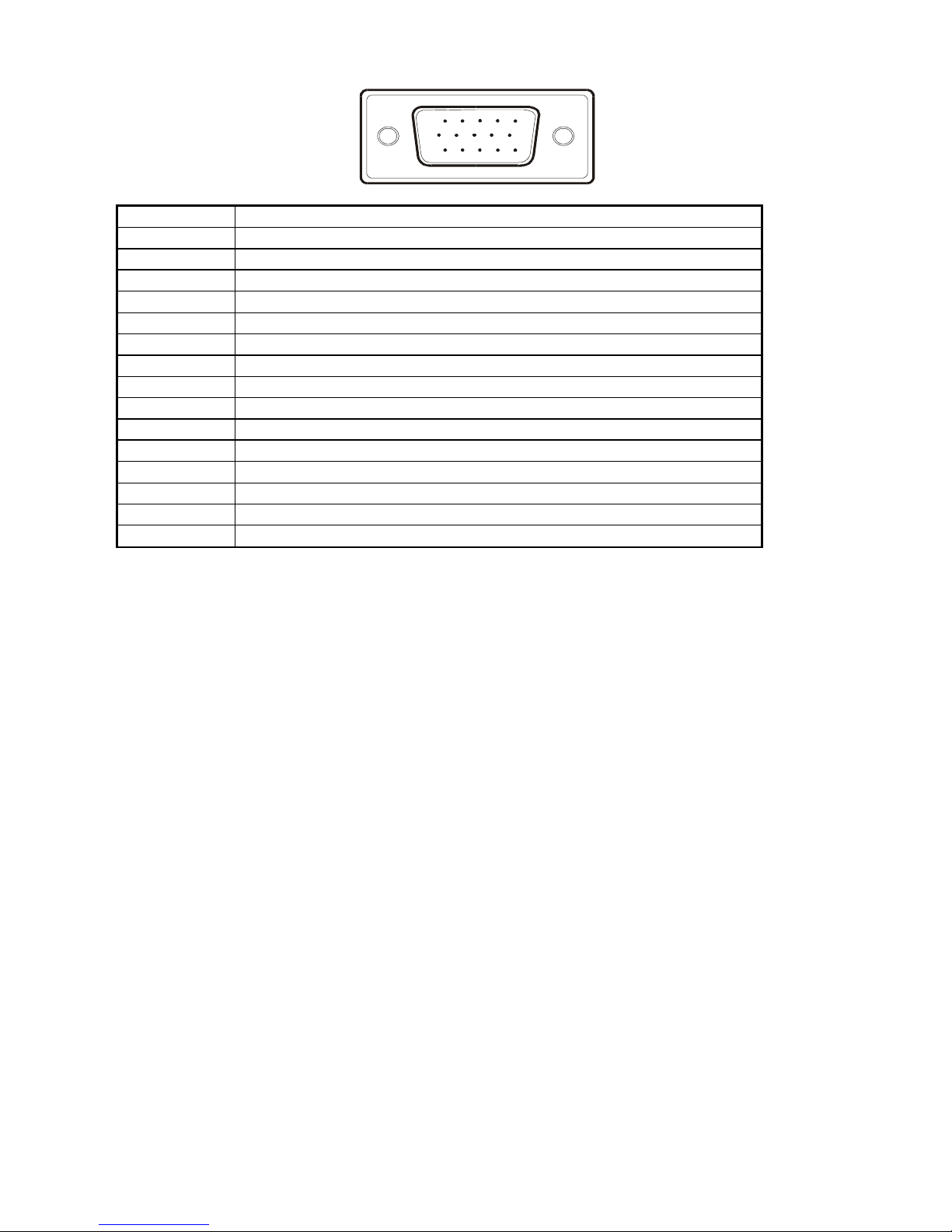
2.2 Interface description
1 5
6
10
11 15
D-SUB connector pin assignment
Pin Number
Pin Function
1 Red video input
2 Green video input
3 Blue video input
4 No Connection
5 Ground
6 Red video ground
7 Green video ground
8 Blue video ground
9 +5V
10 H/V sync ground
11 No connection
12 (SDA)
13 Horizontal sync (Composite sync)
14 Vertical sync
15 (SCL)
Page 7
7
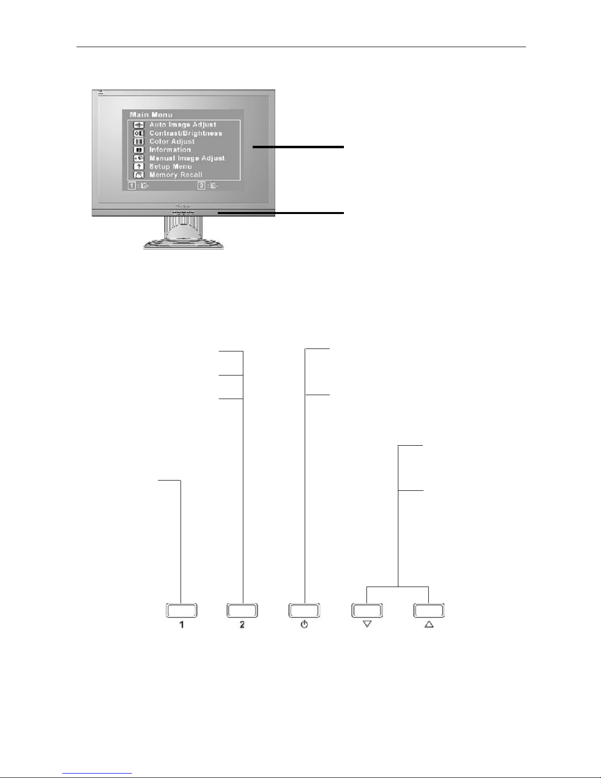
3. Front Panel Function Control Description
“Main Menu Controls”
Main Menu
with OSD controls
Front Control Panel
shown below in detail
Displays the control screen
for the highlighted control.
Also toggles between two
controls on some screens.
Also a shortcut to Auto
Image Adjust.
Displays the
Main Menu or
exits the
control screen
and saves
adjustments.
Power light
Blue = ON
Orange = Power Saving
Standby Power
On/Off
Scrolls through
menu options and
adjusts the
displayed control.
Also a shortcut to
display the
Contrast
adjustment control
screen.
Page 8
8
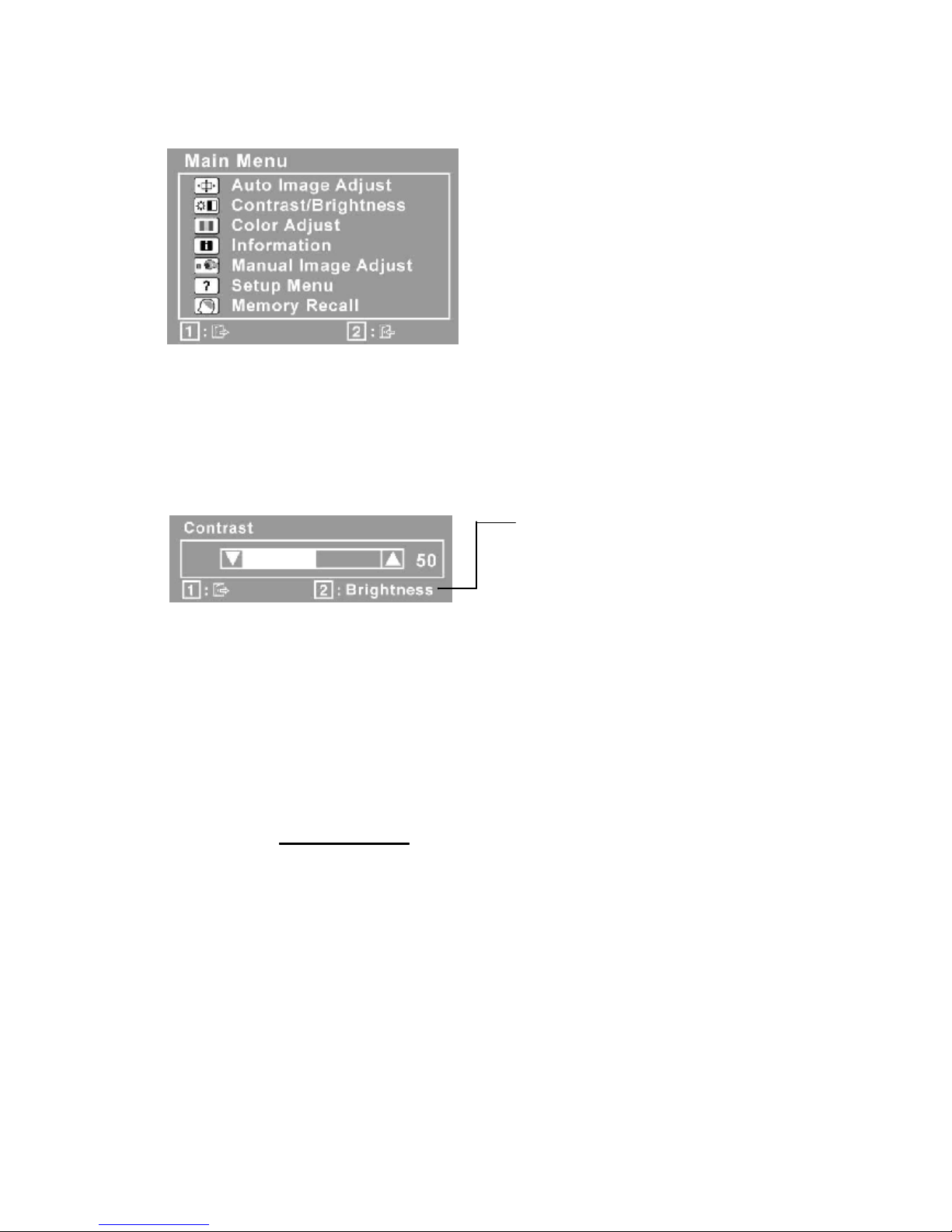
Do the following to adjust the display setting:
1. To display the Main Menu, press button [1].
NOTE: All OSD menus and adjustment screens disappear automatically after about 15
seconds. This is adjustable through the OSD timeout setting in the setup menu.
2. To select a control to adjust, press or to scroll up or down in the Main Menu.
3. After the desired control is selected, press button [2]. A control screen like the one shown
below appears.
The line at the bottom of the screen shows
the current functions of buttons 1 and 2:
Exit or select the Brightness control.
4. To adjust the control, press the up or down buttons.
5. To save the adjustments and exit the menu, press button [1] twice.
The following tips may help you optimize your display:
• Adjust the computer's graphics card so that it outputs a 1366 x 768 @ 60Hz video signal to
the LCD display. (Look for instructions on “changing the refresh rate” in the graphics card's
user guide.)
• If necessary, make small adjustments using H. POSITION and V. POSITION until the
screen image is completely visible. (The black border around the edge of the screen should
barely touch the illuminated “active area” of the LCD display.)
Page 9

9
Main Menu Controls
Adjust the menu items shown below by using the up and down buttons.
Control Explanation
Auto Image Adjust automatically sizes, centers, and fine tunes the video signal
to eliminate waviness and distortion. Press the [2] button to obtain a sharper
image.
NOTE: Auto Image Adjust works with most common video cards. If this
function does not work on your LCD display, then lower the video refresh rate
to 60 Hz and set the resolution to its pre-set value.
Contrast adjusts the difference between the image background (black level)
and the foreground (white level).
Brightness adjusts background black level of the screen image.
Color Adjust provides several color adjustment modes, including preset color
temperatures and a User Color mode which allows independent adjustment of
red (R), green (G), and blue (B). The factory setting for this product is 6500K
(6500 Kelvin).
sRGB-This is quickly becoming the industry standard for color management,
with support being included in many of the latest applications. Enabling this
setting allows the LCD display to more accurately display colors the way they
were originally intended. Enabling the sRGB setting will cause the Contrast and
Brightness adjustments to be disabled.
9300K-Adds blue to the screen image for cooler white (used in most office
settings with fluorescent lighting).
6500K-Adds red to the screen image for warmer white and richer red.
5400K-Adds green to the screen image for a darker color.
User Color Individual adjustments for red (R), green (G), and blue (B).
1. To select color (R, G or B) press button [2].
2. To adjust selected color, press and.
Important: If you select RECALL from the Main Menu when the product is set
to a Preset Timing Mode, colors return to the 6500K factory preset.
Page 10
10
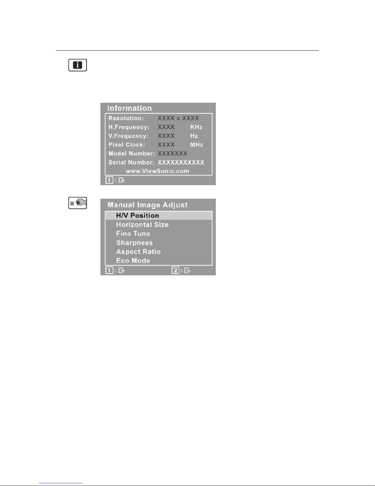
Control Explanation
Information displays the timing mode (video signal input) coming from the
graphics card in the computer, the LCD model number, the serial number, and
the ViewSonic® website URL. See your graphics card’s user guide for
instructions on changing the resolution and refresh rate (vertical frequency).
NOTE: VESA 1366 x 768 @ 60Hz (recommended) means that the resolution is
1366 x 768 and the refresh rate is 60 Hertz.
Manual Image Adjust displays the Manual Image Adjust menu.
H./V. Position (Horizontal/Vertical Position) moves the screen image left or
right and up or down.
H. Size (Horizontal Size) adjusts the width of the screen image.
Fine Tune sharpens the focus by aligning text and/or graphics with pixel
boundaries.
NOTE: Try Auto Image Adjust first.
Sharpness adjusts the clarity and focus of the screen image.
Aspect ratio Selects the image size for 4:3 and full screen.
ECO Mode provides the lower power consumption by reducing the brightness.
Standard: The default brightness setting
Optimize: Decreases the brightness by 25 %
Conserve: Decreases the brightness by 50 %
NOTE: When the ECO Mode is set to "Optimize" or "Conserve", the
Brightness, Contrast, and Dynamic Contrast cannot be adjusted.
Page 11
11
Control Explanation
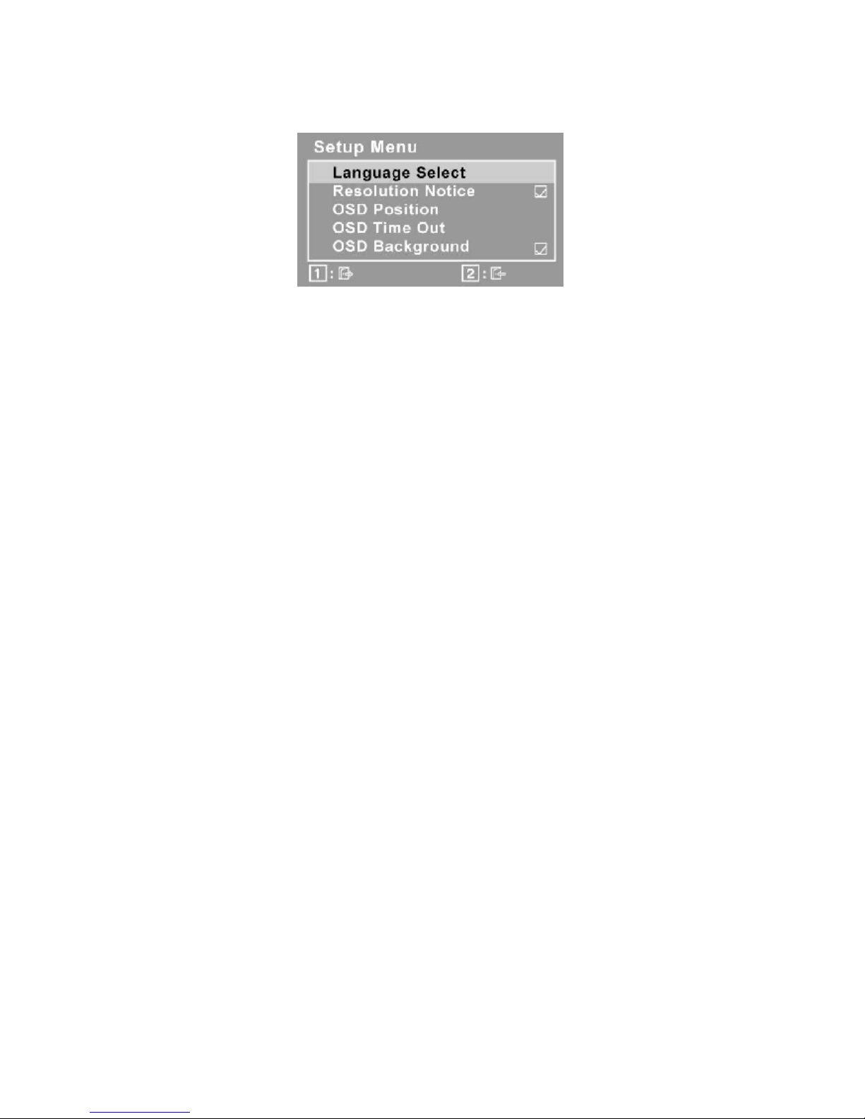
Setup Menu displays the menu shown below:
Language Select allows the user to choose the language used in the menus and
control screens.
Resolution Notice advises the optimal resolution to use.
OSD Position allows the user to move the OSD menus and control screens.
OSD Timeout sets the length of time the OSD screen is displayed. For example,
with a “15 second” setting, if a control is not pushed within 15 seconds, the
display screen disappears.
OSD Background allows the user to turn the OSD background On or Off.
Memory Recall returns the adjustments back to factory settings if the display is
operating in a factory Preset Timing Mode listed in the Specifications of this
manual.
Exception: This control does not affect changes made with the User Color
control, Language Select or Power Lock setting.
Page 12
12
4. Circuit Description
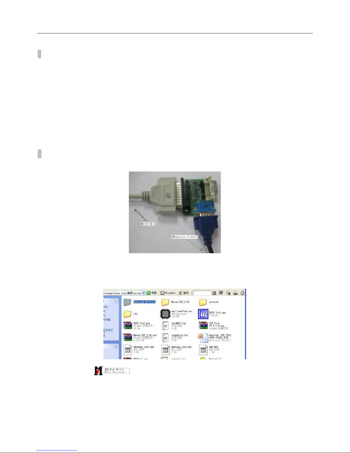
ISP Instruction
1The tool for ISP
1) An i486 (or above) personal computer or compatible.
2) Microsoft operation system Windows 95/98/2000/XP.
3) “ISP_Tool V4.4.1.0” program
4) Software ISP SN Alignment kits
The kit contents:
a) ISP BOARD x1
b) Printer cablex1
c) VGA CABLE X1
2Connect the ISP board as follow:
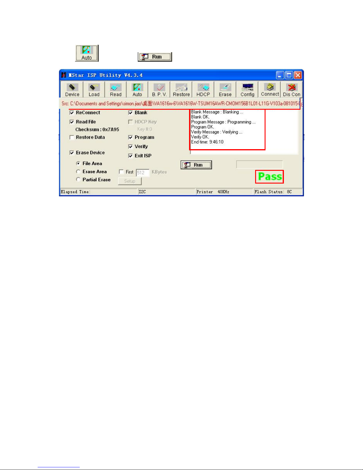
3 The process of ISP write is as follows:
a. Double-click ,running the program as follows:
Page 13
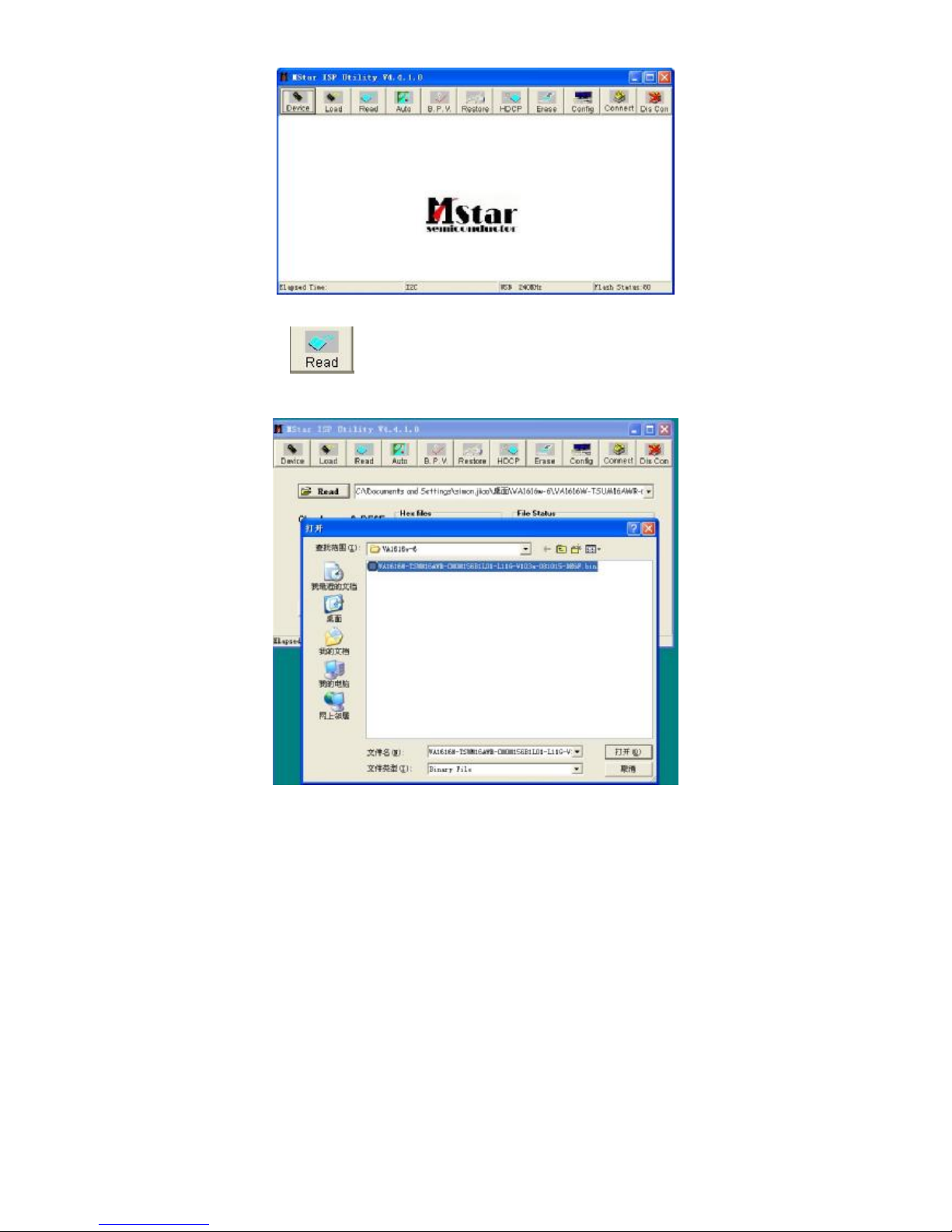
13
b. Select sure, Click icon, search the program
” VA1616W-TSUM16AWR-CMOM156B1L01-L11G-V103a-081015-DE6F.bin” and click save:
Page 14
14
C. Click icon, then click . If it burns successfully, it will show as the follow picture:
Page 15
15
DDC Instruction
1 General
DDC Data Re-programming
In case the main EEPROM with Software DDC which store all factory settings were replaced because a defect,
repaired monitor’ the serial numbers have to be re-programmed.
It is advised to re- soldered the main EEPROM with Software DDC from the old board onto the new board if
circuit board have been replaced, in this case the DDC data does not need to be re-programmed.
Additional information about DDC (Display Data Channel) may be obtained from Video Electronics Standards
Association (VESA). Extended Display Identification Data (EDID) information may be also obtained from
VESA.
1. An i486 (or above) personal computer or compatible.
2. Microsoft operation system Windows 95/98/2000/XP.
3. “PORT95NT.exe, WinDDC_ setup” program.
4. Software OSD SN Alignment kits
The kit contents:
a) OSD SN BOARD x1
b) Printer cablex1
c) VGA cable x1
d) Digital cable x1
e) 12V DC power source
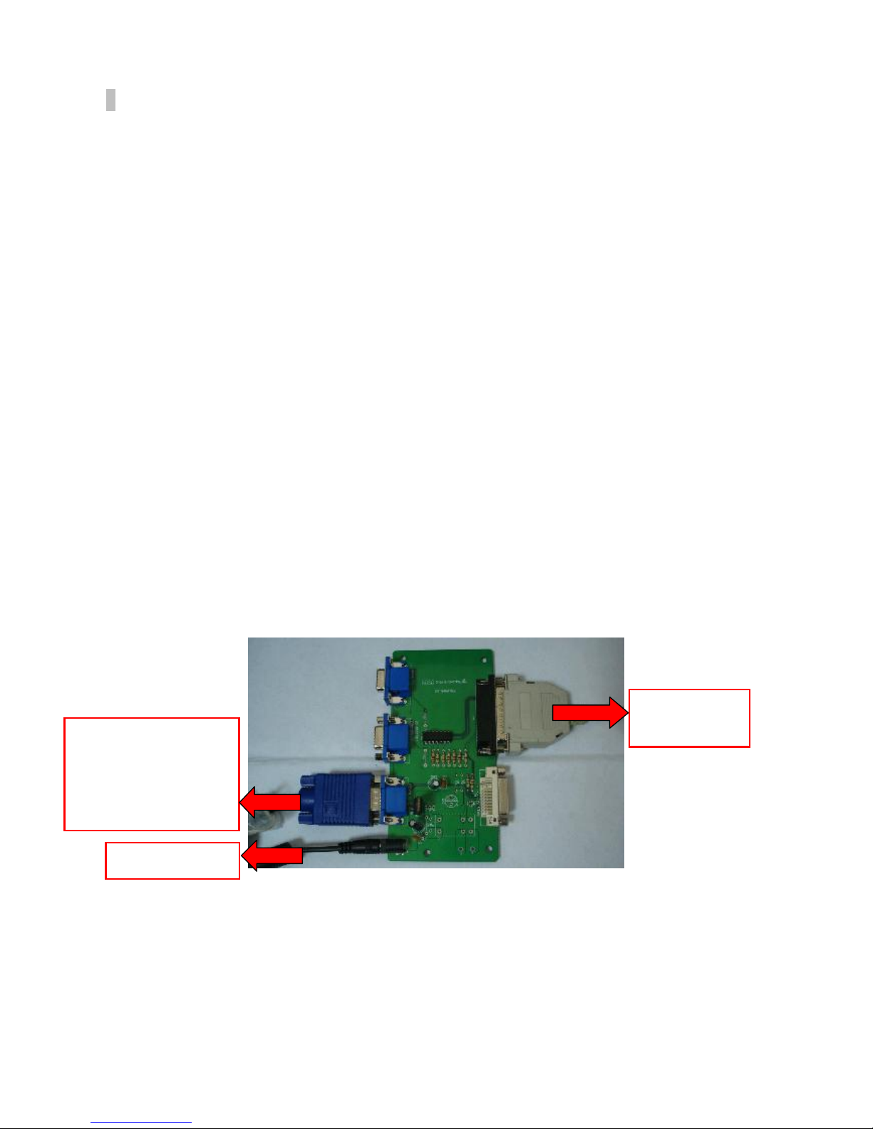
2 Connect the DDC board
Connect to the
PC LPT
When you write analog
EDID, Connect this port
to the VA1616W-6’ VGA
port
1Connect to the
Page 16
16
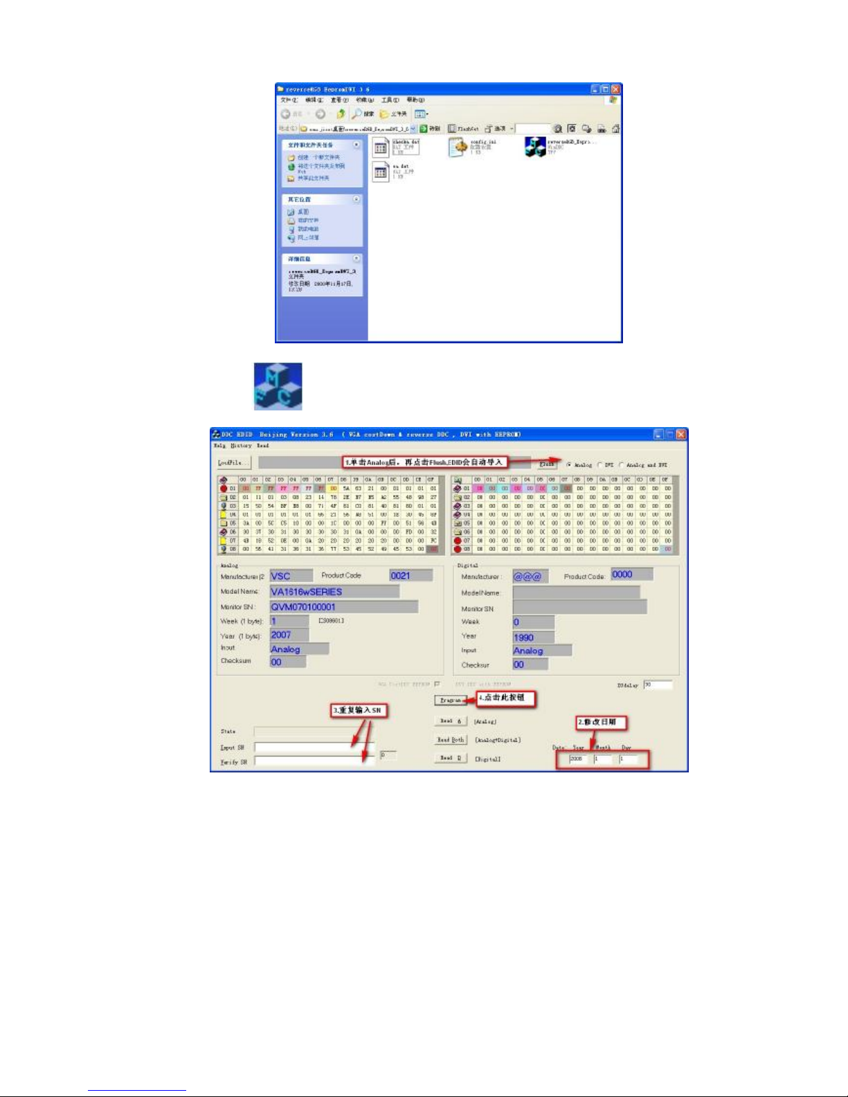
3 The process of analog DDC write is as follow:
Double-click ,appear as follow Figs:
Press “program”,it will show “PASS”,it means download OK.
Note: The way of digital DDC write is the same as analog DDC write.
Page 17

17
5. Adjustment Procedure
1. All Modes Reset
You should do “All Model Reset” (Refer to Chap 3. Hot Keys for Function Controls) first. This action
will allow you to erase all end-user’s settings and restore the factory defaults.
2. Auto Image Adjust
The Auto Adjust is aimed to offer a best screen quality by built-in ASIC. For optimum screen
quality, the user has to adjust each function manually.
A.Turn the computer and LCD monitor on.
B. Press the ‘Auto’ button on monitor keypad to Auto Adjust.
C. The LCD monitor will start the Auto Adjust process automatically and run for 10 consecutive
seconds, during which time you will notice the image change.
3. Firmware
Test Patten: Burn in Model (Refer to Chap3. Hot Keys for Function Control)
-Make sure the F/W is the latest version.
4. DCC
Test Patten: EDID program
-Make sure it can pass test program.
5. Window Shut Down
Test Signal: 1280*1024@60Hz
Test Pattern:
Checkered Pattern Every One Pixel (50%Green & 50%Blue)
Inspection Item: Flicker, Mura
6. Window BG
Test Signal: 1280*1024@60Hz
Test Pattern:
Window standard pattern
Inspection Item: Line Defect, Function Defect & Mura
7. 25 Gray
Test Signal: 1280*1024@60Hz
Test Pattern:
Page 18

18
Full Screen 25% White (Gray)
Inspection Item: Particle, Line Defect & Mura
8. 50 Gray
Test Signal: 1280*1024@60Hz
Test Pattern:
Full Screen 50% White (Gray)
Inspection Item: Bright Dot, Particle, Line Defect & Mura
9. White Box
Test Signal: 1280*1024@60Hz
Test Pattern:
Window standard pattern
Inspection Item: Particle, Line Defect, Power, Image Remain & Mura
10. Black Box
Test Signal: 1280*1024@60Hz
Test Pattern:
Window standard pattern
Inspection Item: Bright Dot, Line Defect & Power
11. RED
Test Signal: 1280*1024@60Hz
Test Pattern:
Full Screen Red
Inspection Item: Bright Dot, Partial & Line Defect
Page 19

19
12. Green
Test Signal: 1280*1024@60Hz
Test Pattern:
Full Screen Green
Inspection Item: Bright Dot, Partial & Line Defect
13. Blue
Test Signal: 1280*1024@60Hz
Test Pattern:
Full Screen Green
Inspection Item: Bright Dot, Partial & Line Defect
14. Gray_Scale_0-100_V64
Test Signal: 1280*1024@60Hz
Test Pattern:
Vertical 64 (256) Gray Scale (Right → Left,From 0 to 100% White)
Inspection Item: Line Defect & Function Defect
15. Function Test Display pattern
Item
Pattern Description Remark
1 Gray_Scale_0-100_V
Vertical 64 (256) Gray Scale (右→左,
From 0
to 100% White)
Figure 1
2 Gray_Scale_0-100_H
Horizontal 64 (256) Gray Scale (上→下,
From
0 to 100% White)
Figure 2
3 Black Full Screen Black Figure 3
4 Red Full Screen 50% Red Figure 4
5 Green Full Screen 50% Green Figure 5
6 Blue Full Screen 50% Blue Figure6
7 White Full Screen White Figure7
8 Black_Tile Black Tile Under White Background Figure 8
Page 20

20
Figure 1 Figure 2
Figure 5
Figure 4
Figure 6
Figure 3
Figure 5
Page 21

21
Factory Defaults
Item Defaults Item Defaults
Contrast 70% Input Priority N/A
Brightness 100% Resolution Notice On
Color Temperature 6500K Volume N/A
Sharpness 100% Balance N/A
OSD H. Position 50% Treble N/A
OSD V. Position 50% Bass N/A
OSD Time Out 15 DCR ON for E / G / P model
Off for M model only
OSD Background On 1280x768 / 1366x768 1366x768
ECO Mode Standard 720x400 / 640x400 720x400
Aspect Ratio Full Screen
Figure 8 Figure 7
Page 22

22
6. Troubleshooting Flow Chart
Page 23

23
No power
• Make sure power button (or switch) is ON.
• Make sure A/C power cord is securely connected to the LCD display.
• Plug another electrical device (like a radio) into the power outlet to verify that the outlet is
supplying proper voltage.
Power is ON but no screen image
• Make sure the video cable supplied with the LCD display is tightly secured to the video
output port on the back of the computer. If the other end of the video cable is not attached
permanently to the LCD display, tightly secure it to the LCD display.
• Adjust brightness and contrast.
• If you are using an Macintosh older than G3, you need a Macintosh adapter.
Wrong or abnormal colors
• If any colors (red, green, or blue) are missing, check the video cable to make sure it is
securely connected. Loose or broken pins in the cable connector could cause an improper
connection.
• Connect the LCD display to another computer.
• If you have an older graphics card, contact ViewSonic® for a non-DDC adapter.
Control buttons do not work
• Press only one button at a time.
Page 24

24
7. Block Diagram
Page 25

25
8. Schematic Diagrams
8.1 main board
8.2 power board
Page 26

5
5
4
4
3
3
2
2
1
1
D D
C C
B B
A A
XGA/SXGA
TSUM16FWR SCHEMATIC
LVDS OUTPUT
Q17W D
AOC Q-series / FSC-AXX-3
A
37Thursday, December 13, 2007
715G2904-D
<>
備註
01.Top
G2904-D-X-X-2-071207
OEM MODEL Size
Rev
Date
Sheet
of
TPV MODEL
PCB NAME
備註
T P V ( Top Victory Electronics Co . , Ltd. )
Key Component
線 路 圖 編 號
04.Output
CMVCC
PB[0..9]
PA[0..1]
PPWR_ON#
PA[4..9]
02.Input
DSUB_R+
DSUB_G+
DSUB_B+
DSUB_V
DSUB_RDSUB_G-
DSUB_B-
DET_CABLE
DSUB_H
DSUB_SOG
DDC1_SDA
DDC1_SCL
DSUB_5V
CMVCC1
VCC3.3
03.Scalar
DSUB_R+
DSUB_G+
DSUB_SOG
DSUB_B+
DSUB_RDSUB_G-
DSUB_BDSUB_H
DSUB_V
Adj_BACKLIGHT
VCC1.8
VCC3.3
PA[0..1]
PB[0..9]
DDC1_SDA
DDC1_SCL
DET_CABLE
on_BACKLIGHT
PPWR_ON#
PANEL_ID#
Volume#
Mute
CMVCC
PA[4..9]
CMVCC1
VCTRL
05.Power
on_BACKLIGHT
Adj_BACKLIGHT
VCC1.8
CMVCC
VCC3.3
Mute
Volume#
PANEL_ID#DSUB_5V
CMVCC1
VCTRL
PA[4..9]
PA[0..1]
PB[0..9]
VCC3.3
CMVCC1
CMVCC1
VCC1.8
CMVCC
CMVCC
DSUB_5V
DSUB_5V
CMVCC
VCC3.3
VCC1.8
CMVCC1
VCC3.3
Page 27

5
5
4
4
3
3
2
2
1
1
D D
C C
B B
A A
緊靠近
U103
緊靠近
U101
According to NDS's request to change
type of R101 from 0402 to 0603.
According to NDS's request to move
the capacitors(C102, C103).
Swap VGA G+ abd VGA R+ for ESD GND.
Swap DSUB_SDA abd DSUB_SCL for ESD GND.
Q17W D
AOC Q-series / FSC-AXX-3
B
47Thursday, December 13, 2007
715G2904-D
<
備>註
02.Input
G2904-D-X-X-2-071207
OEM MODEL Size
Rev
Date
Sheet
of
TPV MODEL
PCB NAME
備註
T P V ( Top Victory Electronics Co . , Ltd. )
Key Component
線 路 圖 編 號
VGA_G-
V_Sync
H_Sync
VGA_B-
VGA_G+
VGA_R-
VGA_B+
VGA_B+
DDC1_SCL
VGA_B-
VGA_R+
DSUB_5V
VGA_G-
VGA_G+
VGA_R-
DSUB_SCL
DDC1_SDA
DSUB_SDA
VGA_R+
V_Sync
VGA_PLUG
VGA_PLUG
VGA_B+
H_Sync
VGA_G+
VGA_R+
DSUB_SCL
DSUB_SDA
GND POWER DGND
DSUB_5V
CMVCC1
VCC3.3
CMVCC1
VCC3.3
C106
0.047uF
U102
AZC099-04S
1
2
3 4
5
6
I/O1
GND
I/O2 I/O3
VDD
I/O4
R117
100R 1/16W 5%
R110
100R 1/16W 5%
C111
5pF/50V
C108
5pF/50V
ZD104
UDZSNP5.6B
1 2
U103
AZC099-04S
1
2
3 4
5
6
I/O1
GND
I/O2 I/O3
VDD
I/O4
C113
0.047uF
FB101
BEAD
1 2
FB102
BEAD
1 2
C104
5pF/50V
R114
100R 1/16W 5%
R112
75R 1/16W 5%
R103 100R 1/16W 5%
C115
NC
R121
10K 1/16W 5%
R101 0R05 1/10W 5%
CN101
DB15
1
6
2
7
3
8
4
9
5
11
12
13
14
15
10
17 16
R107
75R 1/16W 5%
R109
390 OHM 1/16W
C110
0.047uF
R113
100R 1/16W 5%
R118
1K 1/16W 5%
R120
10K 1/16W 5%
R111
100R 1/16W 5%
C109
0.047uF
C114
NC
C101
0.047uF
C102
22pF
C107
0.047uF
R115
100R 1/16W 5%
R102 100R 1/16W 5%
FB103
BEAD
1 2
R105
2K2 1/16W 5%
R116
75R 1/16W 5%
R106
2K2 1/16W 5%
C103
22pF
R108
100R 1/16W 5%
ZD103
UDZSNP5.6B
1 2
C105
0.047uF
R104
100R 1/16W 5%
DDC1_SCL5
DDC1_SDA5
DSUB_H 5
DSUB_V 5
DSUB_R- 5
DSUB_R+ 5
DSUB_G- 5
DSUB_G+ 5
DSUB_SOG 5
DSUB_B- 5
DSUB_B+ 5
DSUB_5V 5
VCC3.3 7
DET_CABLE 5
CMVCC1 7
Page 28

5
5
4
4
3
3
2
2
1
1
D D
C C
B B
A A
LVDS
Max condition for LED:
1. Vcc = 3.3 V
2. Current = 12 mA
FW need to be
modified.
U402
For ID2008
010A
020A
Befor AOC ID2007 OSD
For user data, WB, EDID,
HDCP are saved in
Flash.
U402
SST
Near to Connect
X401
X'TAL
加高
(93G 22-53B-H)
津綻
(93G 22-53-J) 32 pF
CL of SPEC
18 pF 27 pF
Cs and Cd (C411, C412)
56 pF
Normal Function : CL = Cs + ((Cg*Cd)/(Cg+Cd))
P.S : Assume Cs = 4 pF
EMI request to add a resister R456, R457
R452
100R 1/16W 5%
NCM24C04-WMN6TP
NC
R454
R453
100R 1/16W 5%
NC
Without NVRAM
0.22uF16V
R455
NC
For NVRAM
NC
10K 1/16W 5% NC
U403
C419
10K 1/16W 5%
NC
R451
10K 1/16W 5%
100R 1/16W 5% NC
R424
R425, C418 depend on
case.
When NVRAM is used,
POWER_KEY# and PANEL_ID#
will not be used at same
time.
PANEL_ID# and POWER_KEY#
could be optional.
R426 NC or 100R 1/16W 5%
R420NCNC NC or 100R 1/16W 5%
Q17W D
AOC Q-series / FSC-AXX-3
C
57Thursday, December 13, 2007
715G2904-D
<>
備註
03.Scalar
G2904-D-X-X-2-071207
OEM MODEL Size
Rev
Date
Sheet
of
TPV MODEL
PCB NAME
備註
T P V ( Top Victory Electronics Co . , Ltd. )
Key Component
線 路 圖 編 號
KEY1
POWER_KEY#
EE_WP
WP
PA[0..1]
PA[4..9]
PB[0..9]
LED_GRN/BLUE
LED_ORANGE
MSCL
MSDA
EE_WP
MSCL
MSDA
POWER_KEY#
LED_ORANGE
LED_GRN/BLUE
KEY1
KEY_AUTO
KEY_LEFT
LED_GRN/BLUE
KEY_RIGHT
LED_ORANGE
POWER_KEY#
PA1
PB4
PA8
PA6
PB6
PB5
PB1
KEY2
PB9
PA0
PA9
PA7
PB3
PB7
PB0
PA5
PB2
PB8
PA4
KEY2
CMVCC
VCC3.3
VCC3.3
VCC1.8
AVDD
AVDD
VDDC
VDDC
VDDP
VDDP
AVDD
CMVCC1
VCC3.3
VCC3.3
+
C410
10uF/50V
R426 100R 1/16W 5%
R455
NC
U402
SST25LF020A-33-4C-SAE
1
2
3
4 5
6
7
8
CE#
SO
WP#
VSS SI
SCK
HOLD#
VDD
R421
10K 1/16W 5%
C407
0.1uF/16V
R402
0R05 1/16W
R429 NC
R454
NC
TSUM1PFR-LF
U401
13
10
11
8
12
9
7
16
17
4
15
14
21
23
22
24
27
56
1
2
35
36
37
38
39
40
41
42
43
44
45
46
47
48
49
50
34
33
5
6
32
31
52
30
18
19
62
20
28
55
58
59
60
61
63
64
25
26
54
51
53
29573
RIN0P
GIN0P
SOGIN0
BIN0P
RIN0M
GIN0M
BIN0M
HSYNC0
VSYNC0
REXT
REFP
REFM
SDO
SCK
SCZ
SDI
PWM2/GPIO_P24
PWM1/GPIO_P25
XIN
XOUT
LVA2P
LVA2M
LVA1P
LVA1M
LVA0P
LVA0M
LVB3P
LVB3M
LVBCKP
LVBCKM
LVB2P
LVB2M
LVB1P
LVB1M
LVB0P
LVB0M
LVA3M
LVA3P
GND
AVDD_ADC
MODE[1]
MODE[0]
VCTRL
VDDC
DDCA_SDA/RS232_TX
DDCA_SCL/rs232_RX
PWM0/GPIO_P26
GPIO_P15/PWM0
GPIO_P27/PWM1
GPIO_P12
GPIO_P00/SAR1
GPIO_P01/SAR2
GPIO_P06
GPIO_P07
GPIO_P13
GPIO_P14
GPIO_P11/I2C_MDA
GPIO_P10/I2C_MCL
RST
VDDP
VDDC
GND
RSTN
GND
R414 120R 1/16W 5%
R403 390 OHM 1/16W
X401
14.31818MHz
1 2
R432 NC
R412 100R 1/16W 5%
C411 22pF
C413
0.1uF/16V
C429
NC
CN402
NC \ CONN
1
2
3
4
5
6
7
8
C417
0.1uF/16V
R406
10K 1/16W 5%
R405 100R 1/16W 5%
R417
10K 1/16W 5%
C418
NC
R410 120R 1/16W 5%
R418 100R 1/16W 5%
R457 0R05 1/16W
R419 100R 1/16W 5%
R456 0R05 1/16W
C414
0.1uF/16V
C409 0.1uF/16V
R424 NC
R409
20K OHM 1/16W
U403
NC / M24C04-WMN6TP
1
2
3
45
6
7
8
NC
E1
E2
VSSSDA
SCL
WC
VCC
R428
3.9K OHM 1/16W
R451 NC
R407
10K 1/16W 5%
C401
0.1uF/16V
C404
0.1uF/16V
R420 100R 1/16W 5%
R408
10K 1/16W 5%
R413 100R 1/16W 5%
C412 22pF
R425
NC
R404
10K 1/16W 5%
R453
NC
R431 NC
C406
0.1uF/16V
C408
0.22uF16V
C416
0.1uF/16V
C415
0.1uF/16V
FB401
300OHM
R430 NC
R411 100R 1/16W 5%
R427
3.9K OHM 1/16W
R452 NC
CN401
CONN
1
2
3
4
5
6
R401
0R05 1/16W
C403
0.1uF/16V
DDC1_SDA3
DDC1_SCL3
DSUB_V3
DSUB_G-3
DSUB_H3
DSUB_SOG3
DSUB_B-3
DSUB_G+3
DSUB_R+3
DSUB_R-3
DSUB_B+3
PA[0..1] 5
PA[4..9] 5
PB[0..9] 5
PANEL_ID# 7
Volume# 7
VCC3.37
VCC1.87
CMVCC 7
CMVCC17
DET_CABLE 4
PPWR_ON# 6
adj_BACKLIGHT 7
VCTRL 7
Mute 7
on_BACKLIGHT 7
Page 29

5
5
4
4
3
3
2
2
1
1
D D
C C
B B
A A
2006-11-7 Add pull up 4K7 to MVCC
S
D
2
3
AO3401L
1
G
R434 has to be changed
from 0805 to 1206
Q17W D
AOC Q-series / FSC-AXX-3
A
67Friday, December 07, 2007
715G2904-D
<>
備註
04.Output
G2904-D-X-X-2-071207
OEM MODEL Size
Rev
Date
Sheet
of
TPV MODEL
PCB NAME
備註
T P V ( Top Victory Electronics Co . , Ltd. )
Key Component
線 路 圖 編 號
PA1
PA8
PB2
PB6
PB2
PA9
PB3
PB5
PB8
PB8
PA0
PB2
PA5
PA6
PB6
PB9
PB[0..9]
PA9
PB3
PA[0..1]
PB1
PA1
PA7
PB5
PA[4..9]
PA6
PA4
PB4
PA0
PB0
PA5
PB0
PA8
PB7
PA4
PB1
PB4
PA7
PB7
PB9
PB3
PPWR_ON#
PANEL_VCC
PANEL_VCC
CMVCC
FB402
120OHM
R436
100K 1/16W 5%
Q404
PMBS3906
CN403
CONN
1
2
3
4
5
6
7
8
9
10
11
12
13
14
15
16
17
18
19
20
21
22
23
24
25
26
27
28
29
30
Q405
AO3401
R434
330 OHM 1/4W
C420
0.1uF/16V
R435
4K7 1/16W 5%
C419
0.1uF/16V
+
C421
100uF25V
R433
10K 1/16W 5%
PA[4..9]5
PA[0..1]5 PB[0..9]5
PPWR_ON#5
CMVCC 7
Page 30

5
5
4
4
3
3
2
2
1
1
D D
C C
B B
A A
3/16
BAT54C : IF 10mA,VF=0.4V
BAV70 : IF 10mA,VF=0.855V(drop voltage too much)
U404 can use package 232 or 252.
Due to current limit is too low,
change from 93G1004-3 to 93G3004-3.
Q17W D
AOC Q-series / FSC-AXX-3
B
77Friday, December 07, 2007
715G2904-D
<
備>註
05.Power
G2904-D-X-X-2-071207
OEM MODEL Size
Rev
Date
Sheet
of
TPV MODEL
PCB NAME
備註
T P V ( Top Victory Electronics Co . , Ltd. )
Key Component
線 路 圖 編 號
Volume
BKLT-EN
BKLT-VBRI
Mute
C_PANEL_INDEX
Volume
BKLT-ENCMVCC
BKLT-VBRI
CMVCC
MVCC
CMVCC
VCC3.3 VCC3.3
VCC3.3
VCC3.3VCC3.3
VCC3.3
VCC1.8
CMVCC1
CMVCC1
DSUB_5V
VCC3.3
R446
NC
Q410
KN2907AS
R440
4K7 1/16W 5%
Q409
KN2907AS
R439
10K 1/16W 5%
+
C427
100uF25V
R447
10K 1/16W 5%
R448
4K7 1/16W 5%
Q406
2N3904S-RTK/PS
R450 NC
NC
+
C426
100uF25V
C432
0.1uF/16V
C422
0.1uF/16V
R441
1K 1/16W 5%
D402
SM340A
R437
10K 1/16W 5%
+
C423
100uF25V
R449
NC
R442
100R 1/16W 5%
CN404
CONN
1
2
3
4
5
6
7
8
9
FB403 NC
U404
AP1117D33LA
1
2
3
ADJ(GND)
VOUT
VIN
C428
0.1uF/16V
D401
BAT54C
Q408
2N3904S-RTK/PS
C425
NC
Mute 5
adj_BACKLIGHT 5
Volume# 5
on_BACKLIGHT 5
PANEL_ID# 5
VCC3.3 4, 5
VCC1.8 5
CMVCC1 5
CMVCC5, 6 DSUB_5V 5
VCTRL5
Page 31

Power
D817
LL4148
R829
22R 1/8W
R822
1K 1/8W
C821
0.1uF/25V
R837
47K 1/8W
D812
LL4148
R831
1K 1/8W
R802
8.2K 1/10W 1%
R830
NC
+12V
C822
1uF/25V
R832
10K 1/10W 1%
Q805
PDTC144WK
C820
220pF50V
R808
10K 1/10W 1%R820
10K 1/10W 1%
C819
0.0022uF
R817
10K 1/10W 1%
D805
LL4148
D801
BAV99
3
1
2
R851
6K8 1/10W
+
C802
470UF/25V
IC801
TL494IDR
1IN+
1
1IN-
2
FEEDBACK
3
DTC
4
CT
5
RT
6
GND
7
C18E1
9
E2
10
C2
11
VCC
12
OUTPUT CTRL
13
REF
14
2IN-
15
2IN+
16
R828
10K 1/10W 1%
D802
BAV99
3
1
2
C823
0.0022uF
D807
LL4148
Q809
RK7002
F801
0 OHM 1/4W
D806
LL4148
D811
NC
R803
680K 1/10W
R839
22R 1/8W
R850
22R 1/8W
Q811
PMBS3904
Q812
PMBS3906
1
23
Q807
N.C
R804
100R 1/8W
R810
51K OHM 1% 1/8W
R863
10K 1/10W 1%
C803
30pF/3KV
R823
0R05 1/10W 5%
R826
1K 1/8W
D810
NC
R807
10K 1/10W 1%
DIM
ON/OFF
R835
1M 1/10W 5%
CN801
CONN
1
2
C842
0.01uF
C834
0.1uF/25V
R827
1K 1/10W 1%
R824
1K 1/10W 1%
Q802
AM9945N-T1-PF
S
1
G
2
S
3
G
4
D
8
D
7
D
6
D
5
R818
1K 1/10W 1%
Q808
PDTA144WK
R862
1M 1/10W 5%
R825
22R 1/8W
C817
NC D814
LL4148
C838
1500PF/50V
C807
0.1uF/25V
C846
NC
R865NCR864
NC
C835
NC
Q801
PMBS3904
Q806
PMBS3904
新增
穝糤
CN802
CONN
1
2
R853
68K 1/10W
R814
1K5 1/10W 1%
Q804
PMBS3906
1
23
C825
0.1uF/25V
C839
1500PF/50V
C801
30pF/3KV
R801
1K5 1/10W 1%
R854
NC
ASUS VW161
R841
68K OHM 1% 1/10W
R861
NC
C845
2.2uF/16V
R821
1K 1/8W
OEM MODEL Size
Rev
Date
Sheet of
TPV MODEL
PCB NAME
称爹
T P V ( Top Victory Electronics Co . , Ltd. )
Key Component
絬 隔 瓜 絪 腹
PWPC8621MQDD 1
Custom
3 3Monday, February 18, 2008
715G2852-1
ODM MODEL
3.INVERTER
G2852-1-X-X-9-080218
C824
0.1uF
R856
15R 1/4W
T801
POWER X'FMR
637
4
81
R855
15R 1/4W
Page 32

D817
LL4148
R829
22R 1/8W
R822
1K 1/8W
C821
0.1uF/25V
R837
47K 1/8W
D812
LL4148
R831
1K 1/8W
R802
8.2K 1/10W 1%
R830
NC
+12V
C822
1uF/25V
R832
10K 1/10W 1%
Q805
PDTC144WK
C820
220pF50V
R808
10K 1/10W 1%R820
10K 1/10W 1%
C819
0.0022uF
R817
10K 1/10W 1%
D805
LL4148
D801
BAV99
3
1
2
R851
6K8 1/10W
+
C802
470UF/25V
IC801
TL494IDR
1IN+
1
1IN-
2
FEEDBACK
3
DTC
4
CT
5
RT
6
GND
7
C18E1
9
E2
10
C2
11
VCC
12
OUTPUT CTRL
13
REF
14
2IN-
15
2IN+
16
R828
10K 1/10W 1%
D802
BAV99
3
1
2
C823
0.0022uF
D807
LL4148
Q809
RK7002
F801
0 OHM 1/4W
D806
LL4148
D811
NC
R803
680K 1/10W
R839
22R 1/8W
R850
22R 1/8W
Q811
PMBS3904
Q812
PMBS3906
1
23
Q807
N.C
R804
100R 1/8W
R810
51K OHM 1% 1/8W
R863
10K 1/10W 1%
C803
30pF/3KV
R823
0R05 1/10W 5%
R826
1K 1/8W
D810
NC
R807
10K 1/10W 1%
DIM
ON/OFF
R835
1M 1/10W 5%
CN801
CONN
1
2
C842
0.01uF
C834
0.1uF/25V
R827
1K 1/10W 1%
R824
1K 1/10W 1%
Q802
AM9945N-T1-PF
S
1
G
2
S
3
G
4
D
8
D
7
D
6
D
5
R818
1K 1/10W 1%
Q808
PDTA144WK
R862
1M 1/10W 5%
R825
22R 1/8W
C817
NC D814
LL4148
C838
1500PF/50V
C807
0.1uF/25V
C846
NC
R865NCR864
NC
C835
NC
Q801
PMBS3904
Q806
PMBS3904
新增
穝糤
CN802
CONN
1
2
R853
68K 1/10W
R814
1K5 1/10W 1%
Q804
PMBS3906
1
23
C825
0.1uF/25V
C839
1500PF/50V
C801
30pF/3KV
R801
1K5 1/10W 1%
R854
NC
ASUS VW161
R841
68K OHM 1% 1/10W
R861
NC
C845
2.2uF/16V
R821
1K 1/8W
OEM MODEL Size
Rev
Date
Sheet of
TPV MODEL
PCB NAME
称爹
T P V ( Top Victory Electronics Co . , Ltd. )
Key Component
絬 隔 瓜 絪 腹
PWPC8621MQDD 1
Custom
3 3Monday, February 18, 2008
715G2852-1
ODM MODEL
3.INVERTER
G2852-1-X-X-9-080218
C824
0.1uF
R856
15R 1/4W
T801
POWER X'FMR
637
4
81
R855
15R 1/4W
Page 33

33
9. PCB Layout Diagrams
Page 34

CAM350 V 9.0.1 : Mon Sep 22 10:26:29 2008 - (Untitled)
Page 35

CAM350 V 9.0.1 : Mon Sep 22 10:18:22 2008 - (Untitled)
Page 36

CAM350 V 9.0.1 : Mon Sep 22 10:25:46 2008 - (Untitled)
Page 37

CAM350 V 9.0.1 : Mon Sep 22 09:16:28 2008 - (Untitled)
Page 38

37
10. Exploded Diagram and Exploded Parts List
Page 39

38
T67MRHDD2WV2NNN
ViewSonic Model Number:VA1616w-6
Rev:
Item
ViewSonic
P/N Ref. P/N Description Q'ty
1 750GLM56KB112C000Q
PANEL A156B1 VSC
CMO/SF6B101D01
1
2 CBPC8M5VSQ1
CONVERSION
G2904-D-2-VSC-1-080124
1
3 095G8018B3D516 LVDS CABLE 1
4 095G8014 6DN00
WIRE HARNESS 6P(PH)-6P(1253HA
HR)
1
5 PWPC8621MQDD POWER G2852-1-X-X-9-080218 1
6 Q15G0368101 COVER AD 1
7 0M1G1730 6120 SCREW,42-D020523 1
8 0M1G 330 4120 SCREW 42A9930008 4
9 0M1G1740 10120 SCREW 42A9940008 2
10 N52G 1211001 HB
Conductive Tape 155mm *15mm
*0.06mm
2
11 N52G 1211022 HB
Conductive Tape
290mm*15mm*0.06mm
2
12 N52G 1VSC006 HB
Conductive Tape 60mm *24mm
*0.06mm
2
13 705GN834415 FJ BEZEL ASS'Y 40-D022539 1
14 KEPC8QS5 KEY BOARD 1
15 N34G0125 ZK 2A FJ REARCOVER 1
16 0Q1G 130 8120 SCREW 42A9930011 2
17 N34G0132 ZK 1A FJ STAND REAR 40-D022631 1
18 0M1G1740 10120 SCREW 42A9940008 4
19 N33G0064 ZK 1A FJ COVER HINGE 40-D022541 1
20 N34G0134 ZK 1A FJ BASE 40-D022629 1
Page 40

39
11. Recommended Spare Parts List
T67MRHDD2WV3N2
Location
Part No. Description Remark
750GLM56KB112C000Q PANEL A156B1 VSC CMO/SF6B101D01
095G8014 6DN00 WIRE HARNESS 6P(PH)-6P(1253HA HR)
089G414A18N IS POWER CORD 32E1818021
050G 600 1 W WHITE STRAP
N52G 1VSC002 HY Security Tape- 7345511002
N44G6002968 1A CARTON FOR China- 78-D022602
N44G6002VSC 1B Shipping Draw- 79-D022542
N44G9003185 CORNER PAPER 7841595111/78-D004862
N44G9003 90 CORNER PAPER 7841795141
N44G9003 80 CORNER PAPER 78-D004868
N40G 16N968 3A Safety label- 77-D021431
N40G000196855A CARTON LABEL
N40G000296825A HG Warning label- 77-D023227
N40G0001968 2A S/N LABEL 7741513161
N33G0064 ZK 1A FJ COVER HINGE 40-D022541
N23G3155709 1A VIEWSONIC NAME PLATE 77-D000224
705GN734163 FJ SEAT ASSY 40-D022543
705GN834361 FJ REAR COVER ASSY
705GN734161 FJ STAND ASSY 40-D022540
Q15G0368101 MAIN FRAME
0M1G1740 8120
SCREW FOR STD/MF
42-D020715/42-D000649
0M1G 330 4120 SCREW 42A9930008
002G6008 2 SCREW 42-D015647
0Q1G 330 8120 SCREW 3X8mm 42A9930017/ 42-D002093
0M1G1740 10120 SCREW 42A9940008
N45G 88607009 HQ PE BAG FOR MONITOR 78-D023174
N44G6002 1 MZ CUSHION-L 78-D022605
N44G6002 2 MZ CUSHION-R 78-D022594
N45G 52001 PE SHEET
P45G 77001 enlace film
N52G6034 17001 HB MYLAR
N52G 1VSC006 Conductive Tape 60mm *24mm *0.06mm
N52G 1211001 Conductive Tape 155mm *15mm *0.06mm
N52G 2191 01 TAPE /7345911004
N52G6020003 PANEL PROTECTOR FILM 73-D021802
N40G000196840A S/N LABEL- 77-D022604
Page 41

40
089G414A18N YH POWER CORD(32E1818021)
N44G6000 1 1A EMPTY CARTON FOR LOADING
N07G0011 1 HW pallet- 78-D024987
EDIDVSC16A001 CHECKSUM 0x00
PWPC8621MQDD POWER G2852-1-X-X-9-080218
CBPC8M5VSQ1 CONVERSION G2904-D-2-VSC-1-080124
KEPC8QS5 KEY BOARD
N52G 1211001 HB Conductive Tape 155mm *15mm *0.06mm
N23G3178712 1A VSC-BIRD-LOGO 77-D020778
705GN834415 FJ BEZEL ASS'Y 40-D022539
N52G 1VSC006 HB Conductive Tape 60mm *24mm *0.06mm
N52G 1185005 SW Vinegar ache rubberized fabric 19(MM)*30(M)
N52G 1211002 HB Conductive Tape 90mm *24mm *0.06mm
N52G 1211022 HB Conductive Tape 290mm*15mm*0.06mm
N85G 583503 Gasket 15mm*10mm*3mm
095G8018B3D516 LVDS CABLE
089G 728HAA DB D-SUB CABLE
089G 728GAA DB D-SUB CABLE
BIOS16M01201
TSUM16AWR-V101B-080814,CHECKSUM
D787
N34G0134 ZK 1A FJ BASE 40-D022629
0M1G 130 8120 SCREW 42A9930022
N15G0030 1 FH Seat Plate 41-D022648
N12G6300002 SX RUBBER 40A1769201
N34G0125 ZK 2A FJ REARCOVER
N15G0032 1 PLATE_LOCK 40A1599954
N12G6300003 SX RUBBER_CAP 40-D000227
N15G0029 1 FH SURPPORT PLATE 41-D022649
N37G0023 1 FJ HINGE 41-D022650
N34G0131 ZK 1A FJ STADN FRONT 40-D022630
N34G0132 ZK 1A FJ STAND REAR 40-D022631
NQ1G 330 10120 SCREW FOR REAR 42A9930015
N33G0059 ZK 1A FJ Wire Mount 40-D022628
N19G0001 1 FJ spring_mpr2
N34G0130 ZK 1A FJ BEZEL 40-D022627
N33G0057NA7 1P LENS 40-D022651
N33G0058 ZP 1A KEY PAD 40-D022625
N34G0133 ZP 1A FJ DECORATION 40-D022626
040G 45762412B CBPC LABEL
CN401 033G3802 6 WAFER
Page 42

41
CN404 033G3802 9 WAFER 9P RIGHT ANELE PITCH
CN403 033G8027 14 H WAFER 14P 2.0MM DIP
C427 067G 3151014KV EC 105℃ CAP 100uF M 25V
C426 067G 3151014KV EC 105℃ CAP 100uF M 25V
C423 067G 3151014KV EC 105℃ CAP 100uF M 25V
C421 067G 3151014KV EC 105℃ CAP 100uF M 25V
C410 067G215V100 7R LOW E.S.R 10uF M 50V
CN101 088G 35315F H D-SUB 15PIN
X401 093G 22 53 J 14.31818MHZ/32PF/49US
SMTC7MM5VSQ1 MAIN BOARD FOR SMT
U401 056G 562557 IC TSUM1PFR-LF
U404 056G 563 52 IC AP1117D33L-13 TO252-3L DIODES
U102 056G 662 13 IC AZC099-04S SOT23-6L
U103 056G 662 13 IC AZC099-04S SOT23-6L
U402 056G1133 81 SST25LF020A-33-4C-SAE
Q404 057G 417 6 PMBS3906/PHILIPS-SMT(06)
Q408 057G 417 12 T KEC 2N3904S-RTK/PS
Q406 057G 417 12 T KEC 2N3904S-RTK/PS
Q409 057G 417 22 T TRA KN2907AS -60V/-0.6A SOT-23
Q410 057G 417 22 T TRA KN2907AS -60V/-0.6A SOT-23
Q405 057G 763 1 A03401 SOT23 BY AOS(A1)
R457 061G0402000 RST CHIP MAX 0R05 1/16W
R456 061G0402000 RST CHIP MAX 0R05 1/16W
R402 061G0402000 RST CHIP MAX 0R05 1/16W
R401 061G0402000 RST CHIP MAX 0R05 1/16W
R442 061G0402101 RST CHIPR 100 OHM +-5% 1/16W
R426 061G0402101 RST CHIPR 100 OHM +-5% 1/16W
R420 061G0402101 RST CHIPR 100 OHM +-5% 1/16W
R419 061G0402101 RST CHIPR 100 OHM +-5% 1/16W
R418 061G0402101 RST CHIPR 100 OHM +-5% 1/16W
R413 061G0402101 RST CHIPR 100 OHM +-5% 1/16W
R412 061G0402101 RST CHIPR 100 OHM +-5% 1/16W
R411 061G0402101 RST CHIPR 100 OHM +-5% 1/16W
R405 061G0402101 RST CHIPR 100 OHM +-5% 1/16W
R117 061G0402101 RST CHIPR 100 OHM +-5% 1/16W
R102 061G0402101 RST CHIPR 100 OHM +-5% 1/16W
R103 061G0402101 RST CHIPR 100 OHM +-5% 1/16W
R104 061G0402101 RST CHIPR 100 OHM +-5% 1/16W
R108 061G0402101 RST CHIPR 100 OHM +-5% 1/16W
R110 061G0402101 RST CHIPR 100 OHM +-5% 1/16W
Page 43

42
R111 061G0402101 RST CHIPR 100 OHM +-5% 1/16W
R113 061G0402101 RST CHIPR 100 OHM +-5% 1/16W
R114 061G0402101 RST CHIPR 100 OHM +-5% 1/16W
R115 061G0402101 RST CHIPR 100 OHM +-5% 1/16W
R441 061G0402102 RST CHIPR 1 KOHM +-5% 1/16W
R118 061G0402102 RST CHIPR 1 KOHM +-5% 1/16W
R447 061G0402103 RST CHIPR 10 KOHM +-5% 1/16W
R439 061G0402103 RST CHIPR 10 KOHM +-5% 1/16W
R437 061G0402103 RST CHIPR 10 KOHM +-5% 1/16W
R433 061G0402103 RST CHIPR 10 KOHM +-5% 1/16W
R421 061G0402103 RST CHIPR 10 KOHM +-5% 1/16W
R417 061G0402103 RST CHIPR 10 KOHM +-5% 1/16W
R408 061G0402103 RST CHIPR 10 KOHM +-5% 1/16W
R407 061G0402103 RST CHIPR 10 KOHM +-5% 1/16W
R406 061G0402103 RST CHIPR 10 KOHM +-5% 1/16W
R404 061G0402103 RST CHIPR 10 KOHM +-5% 1/16W
R121 061G0402103 RST CHIPR 10 KOHM +-5% 1/16W
R120 061G0402103 RST CHIPR 10 KOHM +-5% 1/16W
R436 061G0402104 RST CHIPR 100 KOHM +-5% 1/16W
R410 061G0402121 RST CHIP 120R 1/16W 5%
R414 061G0402121 RST CHIP 120R 1/16W 5%
R409 061G0402203 RST CHIP 20K 1/16W 5%
R106 061G0402222 RST CHIPR 2.2 KOHM +-5% 1/16W
R105 061G0402222 RST CHIPR 2.2 KOHM +-5% 1/16W
R109 061G0402390 0F RST CHIP 390R 1/16W 1%
R403 061G0402390 0F RST CHIP 390R 1/16W 1%
R427 061G0402392 RST CHIP 3.9K 1/16W 5%
R428 061G0402392 RST CHIP 3.9K 1/16W 5%
R435 061G0402472 RST CHIPR 4.7 KOHM +-5% 1/16W
R440 061G0402472 RST CHIPR 4.7 KOHM +-5% 1/16W
R448 061G0402472 RST CHIPR 4.7 KOHM +-5% 1/16W
R116 061G0402750 RST CHIPR 75 OHM +-5% 1/16W
R112 061G0402750 RST CHIPR 75 OHM +-5% 1/16W
R107 061G0402750 RST CHIPR 75 OHM +-5% 1/16W
R101 061G0603000 RST CHIP MAX 0R05 1/10W
R434 061G1206331 RST CHIPR 330 OHM +-5% 1/4W
C432 065G0402104 15 MLCC 0402 0.1UF K 16V X5R
C428 065G0402104 15 MLCC 0402 0.1UF K 16V X5R
C422 065G0402104 15 MLCC 0402 0.1UF K 16V X5R
C420 065G0402104 15 MLCC 0402 0.1UF K 16V X5R
Page 44

43
C419 065G0402104 15 MLCC 0402 0.1UF K 16V X5R
C417 065G0402104 15 MLCC 0402 0.1UF K 16V X5R
C416 065G0402104 15 MLCC 0402 0.1UF K 16V X5R
C415 065G0402104 15 MLCC 0402 0.1UF K 16V X5R
C401 065G0402104 15 MLCC 0402 0.1UF K 16V X5R
C403 065G0402104 15 MLCC 0402 0.1UF K 16V X5R
C404 065G0402104 15 MLCC 0402 0.1UF K 16V X5R
C406 065G0402104 15 MLCC 0402 0.1UF K 16V X5R
C407 065G0402104 15 MLCC 0402 0.1UF K 16V X5R
C409 065G0402104 15 MLCC 0402 0.1UF K 16V X5R
C413 065G0402104 15 MLCC 0402 0.1UF K 16V X5R
C414 065G0402104 15 MLCC 0402 0.1UF K 16V X5R
C412 065G0402220 31 CHIP 22PF 50V NPO
C411 065G0402220 31 CHIP 22PF 50V NPO
C103 065G0402220 31 CHIP 22PF 50V NPO
C102 065G0402220 31 CHIP 22PF 50V NPO
C408 065G0402224 17 CAP CER 0.22UF -20%-80%
C113 065G0402473 12 CHIP 0.047uF 16V X7R
C110 065G0402473 12 CHIP 0.047uF 16V X7R
C109 065G0402473 12 CHIP 0.047uF 16V X7R
C107 065G0402473 12 CHIP 0.047uF 16V X7R
C106 065G0402473 12 CHIP 0.047uF 16V X7R
C105 065G0402473 12 CHIP 0.047uF 16V X7R
C101 065G0402473 12 CHIP 0.047uF 16V X7R
C104 065G0402509 31 CHIP 5pF 50V NPO
C108 065G0402509 31 CHIP 5pF 50V NPO
C111 065G0402509 31 CHIP 5pF 50V NPO
FB402 071G 56K121 M CHIP BEAD
FB401 071G 56V301 B CHIP BEAD FCM2012VF-301T07 bullwill
FB101 071G 59K190 B 19 OHM BEAD
FB102 071G 59K190 B 19 OHM BEAD
FB103 071G 59K190 B 19 OHM BEAD
D401 093G 64 33 DIO SIG SM BAV99 (PHSE)R
ZD103 093G 39S 34 T UDZSNP5.6B ROHM
ZD104 093G 39S 34 T UDZSNP5.6B ROHM
D402 093G3004 3 SM340A
715G2904 1 2 MAIN PCB FR-4 57x64x1.6mm DS
SMTKEPC8QV2 KEY BOARD FOR SMT
CN001 033G8032 6F HR CONNECTOR
R003 061G0603200 1F RST CHIPR 2 KOHM +-1% 1/10W
Page 45

44
R004 061G0603200 1F RST CHIPR 2 KOHM +-1% 1/10W
R001 061G0603300 1F RST CHIPR 3 KOHM +-1% 1/10W
R002 061G0603300 1F RST CHIPR 3 KOHM +-1% 1/10W
SW005 077G 604 2 TO TACT 5W BY TOUKE TS-9-TMG-553
SW004 077G 604 2 TO TACT 5W BY TOUKE TS-9-TMG-553
SW003 077G 604 2 TO TACT 5W BY TOUKE TS-9-TMG-553
SW002 077G 604 2 TO TACT 5W BY TOUKE TS-9-TMG-553
SW001 077G 604 2 TO TACT 5W BY TOUKE TS-9-TMG-553
LED001 081G 63O 1 GP LED GPTS0603OC3-PB
LED002 081G0603 B GP LED GPTS06033BC1 GP
715G3270 1 KEY PCB FR-4 77.5x11.8x1.0mm
T67MRHDD2WVSNND
Location
Part No. Description Remark
750GLM56KB112C000Q PANEL A156B1 VSC CMO/SF6B101D01
089G 728HAA DB D-SUB CABLE
089G 728GAA DB D-SUB CABLE
089G414A18N IS POWER CORD 32E1818021
050G 600 1 W WHITE STRAP
N52G 1VSC002 HY Security Tape- 7345511002
N44G6002968 1A CARTON FOR China- 78-D022602
N44G6002VSC 1B Shipping Draw- 79-D022542
N44G9003185 CORNER PAPER 7841595111/78-D004862
N44G9003 90 CORNER PAPER 7841795141
N44G9003 80 CORNER PAPER 78-D004868
N40G 16N968 3A Safety label- 77-D021431
N40G000196855A CARTON LABEL
N40G000296825A HG Warning label- 77-D023227
N40G0001968 2A S/N LABEL 7741513161
N33G0064 ZK 1A FJ COVER HINGE 40-D022541
705GN834415 FJ BEZEL ASS'Y 40-D022539
N34G0134 ZK 1A FJ BASE 40-D022629
N37G0023 1 CX HINGE 41-D022650
N34G0125 ZK 2A FJ REARCOVER
Q15G0368101 MAIN FRAME
0M1G 330 4120 SCREW 42A9930008
002G6008 2 SCREW 42-D015647
0Q1G 330 8120 SCREW 3X8mm 42A9930017/ 42-D002093
0M1G1740 10120 SCREW 42A9940008
N45G 88607009 HQ PE BAG FOR MONITOR 78-D023174
Page 46

45
N44G6002 1 MZ CUSHION-L 78-D022605
N44G6002 2 MZ CUSHION-R 78-D022594
N45G 52001 PE SHEET
P45G 77001 enlace film
N52G6034 17001 HB MYLAR
N52G 1VSC006 Conductive Tape 60mm *24mm *0.06mm
N52G 1211001 Conductive Tape 155mm *15mm *0.06mm
N52G 2191 01 TAPE /7345911004
N52G6020003 PANEL PROTECTOR FILM 73-D021802
N40G000196870A S/N LABEL FOR VA1616W
089G414A18N YH POWER CORD(32E1818021)
N44G6000 1 1A EMPTY CARTON FOR LOADING
N07G0011 1 HW pallet- 78-D024987
PWPC8621MQDD POWER G2852-1-X-X-9-080218
N52G 1211001 HB Conductive Tape 155mm *15mm *0.06mm
EDIDVSC16A003 CHECKSUM 0X9E
CBPC8M5VSQ1 CONVERSION G2904-D-2-VSC-1-080124
KEPC8QS5 KEY BOARD
095G8014 6DN00 WIRE HARNESS 6P(PH)-6P(1253HA HR)
095G8018B3D516 LVDS CABLE
N41G6002968 5A MANUAL
N41G780P968 1A WARRANTY CARD- 78-D021250
F40G 16N968 5A SAFETY LABEL
N40G000296838A Energy Star Label
N40G000296810A LABEL HI-POT-PASS 77-D005237
F40G000296821A ZA Supplier label
N40G000296811C ZA Customer label on Carton
N40G000296813B ZA QC PASS LABEL
N23G3155709 1A VIEWSONIC NAME PLATE 77-D000224
N23G3178712 1A VSC-BIRD-LOGO 77-D020778
N15G0030 1 FH Seat Plate 41-D022648
N12G6300002 SX RUBBER 40A1769201
N15G0032 1 PLATE_LOCK 40A1599954
N12G6300003 SX RUBBER_CAP 40-D000227
N15G0029 1 FH SURPPORT PLATE 41-D022649
N34G0131 ZK 1A FJ STADN FRONT 40-D022630
N34G0132 ZK 1A FJ STAND REAR 40-D022631
NQ1G 330 10120 SCREW FOR REAR 42A9930015
N33G0059 ZK 1A FJ Wire Mount 40-D022628
N19G0001 1 FJ spring_mpr2
Page 47

46
N52G 1VSC006 HB Conductive Tape 60mm *24mm *0.06mm
N52G 1185005 SW Vinegar ache rubberized fabric 19(MM)*30(M)
N52G 1211002 HB Conductive Tape 90mm *24mm *0.06mm
N52G 1211022 HB Conductive Tape 290mm*15mm*0.06mm
0M1G1730 6120 SCREW,42-D020523
0Q1G 130 8120 SCREW 42A9930011
N85G 583503 Gasket 15mm*10mm*3mm
N52G6033 17001 HB MYLAR
BIOS16M01201
TSUM16AWR-V101B-080814,CHECKSUM
D787
N34G0130 ZK 1A FJ BEZEL 40-D022627
N33G0057NA7 1P LENS 40-D022651
N33G0058 ZP 1A KEY PAD 40-D022625
N34G0133 ZP 1A FJ DECORATION 40-D022626
040G 45762412B CBPC LABEL
CN401 033G3802 6 WAFER
CN404 033G3802 9 WAFER 9P RIGHT ANELE PITCH
CN403 033G8027 14 H WAFER 14P 2.0MM DIP
C427 067G 3151014KV EC 105℃ CAP 100uF M 25V
C426 067G 3151014KV EC 105℃ CAP 100uF M 25V
C423 067G 3151014KV EC 105℃ CAP 100uF M 25V
C421 067G 3151014KV EC 105℃ CAP 100uF M 25V
C410 067G215V100 7R LOW E.S.R 10uF M 50V
CN101 088G 35315F H D-SUB 15PIN
X401 093G 22 53 J 14.31818MHZ/32PF/49US
SMTC7MM5VSQ1 MAIN BOARD FOR SMT
U401 056G 562557 IC TSUM1PFR-LF
U404 056G 563 52 IC AP1117D33L-13 TO252-3L DIODES
U102 056G 662 13 IC AZC099-04S SOT23-6L
U103 056G 662 13 IC AZC099-04S SOT23-6L
U402 056G1133 81 SST25LF020A-33-4C-SAE
Q404 057G 417 6 PMBS3906/PHILIPS-SMT(06)
Q408 057G 417 12 T KEC 2N3904S-RTK/PS
Q406 057G 417 12 T KEC 2N3904S-RTK/PS
Q409 057G 417 22 T TRA KN2907AS -60V/-0.6A SOT-23
Q410 057G 417 22 T TRA KN2907AS -60V/-0.6A SOT-23
Q405 057G 763 1 A03401 SOT23 BY AOS(A1)
R457 061G0402000 RST CHIP MAX 0R05 1/16W
R456 061G0402000 RST CHIP MAX 0R05 1/16W
R402 061G0402000 RST CHIP MAX 0R05 1/16W
Page 48

47
R401 061G0402000 RST CHIP MAX 0R05 1/16W
R442 061G0402101 RST CHIPR 100 OHM +-5% 1/16W
R426 061G0402101 RST CHIPR 100 OHM +-5% 1/16W
R420 061G0402101 RST CHIPR 100 OHM +-5% 1/16W
R419 061G0402101 RST CHIPR 100 OHM +-5% 1/16W
R418 061G0402101 RST CHIPR 100 OHM +-5% 1/16W
R413 061G0402101 RST CHIPR 100 OHM +-5% 1/16W
R412 061G0402101 RST CHIPR 100 OHM +-5% 1/16W
R411 061G0402101 RST CHIPR 100 OHM +-5% 1/16W
R405 061G0402101 RST CHIPR 100 OHM +-5% 1/16W
R117 061G0402101 RST CHIPR 100 OHM +-5% 1/16W
R102 061G0402101 RST CHIPR 100 OHM +-5% 1/16W
R103 061G0402101 RST CHIPR 100 OHM +-5% 1/16W
R104 061G0402101 RST CHIPR 100 OHM +-5% 1/16W
R108 061G0402101 RST CHIPR 100 OHM +-5% 1/16W
R110 061G0402101 RST CHIPR 100 OHM +-5% 1/16W
R111 061G0402101 RST CHIPR 100 OHM +-5% 1/16W
R113 061G0402101 RST CHIPR 100 OHM +-5% 1/16W
R114 061G0402101 RST CHIPR 100 OHM +-5% 1/16W
R115 061G0402101 RST CHIPR 100 OHM +-5% 1/16W
R441 061G0402102 RST CHIPR 1 KOHM +-5% 1/16W
R118 061G0402102 RST CHIPR 1 KOHM +-5% 1/16W
R447 061G0402103 RST CHIPR 10 KOHM +-5% 1/16W
R439 061G0402103 RST CHIPR 10 KOHM +-5% 1/16W
R437 061G0402103 RST CHIPR 10 KOHM +-5% 1/16W
R433 061G0402103 RST CHIPR 10 KOHM +-5% 1/16W
R421 061G0402103 RST CHIPR 10 KOHM +-5% 1/16W
R417 061G0402103 RST CHIPR 10 KOHM +-5% 1/16W
R408 061G0402103 RST CHIPR 10 KOHM +-5% 1/16W
R407 061G0402103 RST CHIPR 10 KOHM +-5% 1/16W
R406 061G0402103 RST CHIPR 10 KOHM +-5% 1/16W
R404 061G0402103 RST CHIPR 10 KOHM +-5% 1/16W
R121 061G0402103 RST CHIPR 10 KOHM +-5% 1/16W
R120 061G0402103 RST CHIPR 10 KOHM +-5% 1/16W
R436 061G0402104 RST CHIPR 100 KOHM +-5% 1/16W
R410 061G0402121 RST CHIP 120R 1/16W 5%
R414 061G0402121 RST CHIP 120R 1/16W 5%
R409 061G0402203 RST CHIP 20K 1/16W 5%
R106 061G0402222 RST CHIPR 2.2 KOHM +-5% 1/16W
R105 061G0402222 RST CHIPR 2.2 KOHM +-5% 1/16W
Page 49

48
R109 061G0402390 0F RST CHIP 390R 1/16W 1%
R403 061G0402390 0F RST CHIP 390R 1/16W 1%
R427 061G0402392 RST CHIP 3.9K 1/16W 5%
R428 061G0402392 RST CHIP 3.9K 1/16W 5%
R435 061G0402472 RST CHIPR 4.7 KOHM +-5% 1/16W
R440 061G0402472 RST CHIPR 4.7 KOHM +-5% 1/16W
R448 061G0402472 RST CHIPR 4.7 KOHM +-5% 1/16W
R116 061G0402750 RST CHIPR 75 OHM +-5% 1/16W
R112 061G0402750 RST CHIPR 75 OHM +-5% 1/16W
R107 061G0402750 RST CHIPR 75 OHM +-5% 1/16W
R101 061G0603000 RST CHIP MAX 0R05 1/10W
R434 061G1206331 RST CHIPR 330 OHM +-5% 1/4W
C432 065G0402104 15 MLCC 0402 0.1UF K 16V X5R
C428 065G0402104 15 MLCC 0402 0.1UF K 16V X5R
C422 065G0402104 15 MLCC 0402 0.1UF K 16V X5R
C420 065G0402104 15 MLCC 0402 0.1UF K 16V X5R
C419 065G0402104 15 MLCC 0402 0.1UF K 16V X5R
C417 065G0402104 15 MLCC 0402 0.1UF K 16V X5R
C416 065G0402104 15 MLCC 0402 0.1UF K 16V X5R
C415 065G0402104 15 MLCC 0402 0.1UF K 16V X5R
C401 065G0402104 15 MLCC 0402 0.1UF K 16V X5R
C403 065G0402104 15 MLCC 0402 0.1UF K 16V X5R
C404 065G0402104 15 MLCC 0402 0.1UF K 16V X5R
C406 065G0402104 15 MLCC 0402 0.1UF K 16V X5R
C407 065G0402104 15 MLCC 0402 0.1UF K 16V X5R
C409 065G0402104 15 MLCC 0402 0.1UF K 16V X5R
C413 065G0402104 15 MLCC 0402 0.1UF K 16V X5R
C414 065G0402104 15 MLCC 0402 0.1UF K 16V X5R
C412 065G0402220 31 CHIP 22PF 50V NPO
C411 065G0402220 31 CHIP 22PF 50V NPO
C103 065G0402220 31 CHIP 22PF 50V NPO
C102 065G0402220 31 CHIP 22PF 50V NPO
C408 065G0402224 17 CAP CER 0.22UF -20%-80%
C113 065G0402473 12 CHIP 0.047uF 16V X7R
C110 065G0402473 12 CHIP 0.047uF 16V X7R
C109 065G0402473 12 CHIP 0.047uF 16V X7R
C107 065G0402473 12 CHIP 0.047uF 16V X7R
C106 065G0402473 12 CHIP 0.047uF 16V X7R
C105 065G0402473 12 CHIP 0.047uF 16V X7R
C101 065G0402473 12 CHIP 0.047uF 16V X7R
Page 50

49
C104 065G0402509 31 CHIP 5pF 50V NPO
C108 065G0402509 31 CHIP 5pF 50V NPO
C111 065G0402509 31 CHIP 5pF 50V NPO
FB402 071G 56K121 M CHIP BEAD
FB401 071G 56V301 B CHIP BEAD FCM2012VF-301T07 bullwill
FB101 071G 59K190 B 19 OHM BEAD
FB102 071G 59K190 B 19 OHM BEAD
FB103 071G 59K190 B 19 OHM BEAD
D401 093G 64 33 DIO SIG SM BAV99 (PHSE)R
ZD103 093G 39S 34 T UDZSNP5.6B ROHM
ZD104 093G 39S 34 T UDZSNP5.6B ROHM
D402 093G3004 3 SM340A
715G2904 1 2 MAIN PCB FR-4 57x64x1.6mm DS
SMTKEPC8QV2 KEY BOARD FOR SMT
CN001 033G8032 6F HR CONNECTOR
R003 061G0603200 1F RST CHIPR 2 KOHM +-1% 1/10W
R004 061G0603200 1F RST CHIPR 2 KOHM +-1% 1/10W
R001 061G0603300 1F RST CHIPR 3 KOHM +-1% 1/10W
R002 061G0603300 1F RST CHIPR 3 KOHM +-1% 1/10W
SW005 077G 604 2 TO TACT 5W BY TOUKE TS-9-TMG-553
SW004 077G 604 2 TO TACT 5W BY TOUKE TS-9-TMG-553
SW003 077G 604 2 TO TACT 5W BY TOUKE TS-9-TMG-553
SW002 077G 604 2 TO TACT 5W BY TOUKE TS-9-TMG-553
SW001 077G 604 2 TO TACT 5W BY TOUKE TS-9-TMG-553
LED001 081G 63O 1 GP LED GPTS0603OC3-PB
LED002 081G0603 B GP LED GPTS06033BC1 GP
715G3270 1 KEY PCB FR-4 77.5x11.8x1.0mm
Page 51

50
12. Different Parts List
Diversity of T67MRHDD2WVSNND compared with T67MRHDD2WV3N2
Location Part No. Description Remark
N37G0023 1 CX HINGE 41-D022650
N40G000196870A S/N LABEL FOR VA1616W
EDIDVSC16A003 CHECKSUM 0X9E
N41G6002968 5A MANUAL
N41G780P968 1A WARRANTY CARD- 78-D021250
F40G 16N968 5A SAFETY LABEL
N40G000296838A Energy Star Label
N40G000296810A LABEL HI-POT-PASS 77-D005237
F40G000296821A ZA Supplier label
N40G000296811C ZA Customer label on Carton
N40G000296813B ZA QC PASS LABEL
0M1G1730 6120 SCREW,42-D020523
0Q1G 130 8120 SCREW 42A9930011
N52G6033 17001 HB MYLAR
Page 52

51
* Reader’s Response*
Dear Readers:
Thank you in advance for your feedback on our Service Manual, which allows continuous improvement
of our products. We would appreciate your completion of the Assessment Matrix below, for return to
ViewSonic Corporation.
Assessment
A. What do you think about the content of this Service Manual?
Unit Excellent
Good Fair Bad
1. Precautions and Safety Notices
2. Specification
3. Front Panel Function Control Description
4. Circuit Description
5. Adjustment Procedure
6. Troubleshooting Flow Chart
7. Block Diagrams
8. Schematic Diagrams
9.PCB Layout Diagrams
10. Exploded Diagram and Exploded Parts List
11. Recommended Spare Parts List
B. Are you satisfied with this Service Manual?
Item Excellent Good Fair Bad
1. Service Manual Content
2. Service Manual Layout
3. The form and listing
C. Do you have any other opinions or suggestions regarding this service manual?
Reader’s basic dada:
Name:
Title:
Company:
Add:
Tel:
Fax:
E-mail:
After completing this form, please return it to ViewSonic Quality Assurance in the USA at facsimile
1-909-839-7943. You may also e-mail any suggestions to the Director, Quality Systems & Processes
(marc.maupin@viewsonic.com)
 Loading...