

Page 1

Service Manual
LCD TV N1750w-1
Model No. VS10621
ViewSonic
(N1750W-1_SM_- Rev. 1 – January 30, 2005)
381 Brea Canyon Road, Walnut, California 91789 USA - (800) 888-8583
Page 2

Preface
Copyright © ViewSonic Corporation, 2004. All rights reserved.
Macintosh and Power Macintosh are registered trademarks of Apple Computer, Inc.
Microsoft, Windows, Windows NT, and the Windows logo are registered trademarks of Microsoft Corporation in the United
States and other countries.
ViewSonic, the three birds logo, OnView, ViewMatch, and ViewMeter are registered trademarks of ViewSonic Corporation.
VESA is a registered trademark of the Video Electronics Standards Association. DPMS and DDC are trademarks of VESA.
Disclaimer: ViewSonic Corporation shall not be liable for technical, editorial errors, or omissions contained herein; nor for
incidental or consequential damages resulting from furnishing this material, or the performance or use of this product.
In the interest of continuing product improvement, ViewSonic Corporation reserves the right to change product specifications
without notice. Information in this document may change without notice. For the most recent version of this document, please check
www.viewsonic.com.
No part of this document may be copied, reproduced, or transmitted by any means, for any purpose without prior written permission
from ViewSonic Corporation.
Important safety information
1. Read these instructions.
2. Keep these instructions.
3. Heed all warnings.
4. Follow all instructions.
5. Do not use this apparatus near water.
6. Clean only with a dry cloth.
7. Do not block any of the ventilation openings. Install in accordance with the manufacturers instructions.
8. Do not install near any heat sources such as radiators, heat registers, stoves, or other apparatus (including amplifiers) that produce
heat.
9. Do not defeat the safety purpose of the polarized or grounding type plug. A polarized plug has two blades with one wider than the
other. A grounding type plug has two blades and third grounding prong. The wide blade or third prong is provided for your safety.
When the provided plug does not fit into your outlet, consult an electrician for replacement of the obsolete outlet.
10. Protect the power cord from being walked on or pinched particularly at plugs, convenience receptacles, and the point where they
exit from the apparatus.
11. Only use attachments/accessories specified by the manufacturer.
12. Use only with a cart, stand, tripod, bracket, or table specified by the manufacturer, or sold with the apparatus. When a cart is used,
use caution when moving the cart/apparatus combination to avoid injury from tip-over.
13. The TV should be operated only from the type of power source indicated on the label. If you are not sure of the type of power
supplied to your home, consult your dealer or local power company.
14. Unplug this apparatus during lightning storms or when unused for long periods of time.
15. Refer all servicing to qualified service personnel. Servicing is required when the apparatus has been damaged in any way, such
as power-supply cord or plug is damaged, liquid has been spilled or objects have fallen into apparatus, the apparatus has been
exposed to rain or moisture, does not operate normally, or has been dropped.
16. This product may contain lead or mercury. Disposal of these materials may be regulated due to environmental considerations.
For disposal or recycling information, please contact your local authorities or the Electronic Industries Alliance: www.eiae.org
17. Damage Requiring Service – The appliance should be serviced by qualified service personnel when:
ViewSonic Corporation N1750w
2
Page 3

A. The power supply cord or the plug has been damaged; or
B. Objects have fallen, or liquid has been spilled into the appliance; or
C. The appliance has been exposed to rain; or
D. The appliance does not appear to operate normally or exhibits a marked change in performance; or
E. The appliance has been dropped, or the enclosure damaged.
18. Tilt/Stability – All televisions must comply with recommended international global safety standards for tilt and stability
properties of its cabinets design.
! Do not compromise these design standards by applying excessive pull force to the front,
or top, of the cabinet, which could ultimately overturn the product.
! Also, do not endanger yourself, or children, by placing electronic equipment/toys on the top of the cabinet. Such items could
unsuspectingly fall from the top of the set and cause product damage and/or personal injury.
19. Wall or Ceiling Mounting – The appliance should be mounted to a wall or ceiling only as recommended by the manufacturer.
20. Power Lines – An outdoor antenna should be located away from power lines.
21. Outdoor Antenna Grounding – If an outside antenna is connected to the receiver, be sure the antenna system is grounded so as
to provide some protection against voltage surges and built up static charges. Section 810 of the National Electric Cord,
ANSI/NFPA No. 70-1984, provides information with respect to proper grounding of the mats and supporting structure grounding
of the lead-in wire to an antenna-discharge unit, size of grounding connectors, location of antenna-discharge unit, connection to
grounding electrodes and requirements for the grounding electrode. See Figure below.
22. Objects and Liquid Entry – Care should be taken so that objects do not fall and liquids are not spilled into the enclosure
through openings.
ViewSonic Corporation N1750w
3
Page 4

Table of contents
Table of contents …………………………………………………………………………………… 4
Revision list…………………………………………………………………………………….…. 5
1. Specifications …...............................................................................................…………...…..
1.1 General specifications ….......................................................................…………....…. 6
1.2 LCD TV description ..................................................……………….……...………….. 7
1.3 Interface connector ......................................................……………………….….....…. 7
1.4 D-Sub pin distribution ...............................................................…………...………….. 7
1.5 Factory preset display modes ....................................…………………………….....…. 8
2. Theory of operation.................................................................……………...…………………. 8
2.1 Video.............................………...................................................................………….... 8
2.2 Audio ...........................................................................................................………….... 9
2.3 Electrical .......................................................................................................…………... 9
3. Adjustment............................................................................................................…………..... 10
3.1 Front panel adjustment………………………………………………….……………… 10
3.2 How to use the menu…………………………………………………………………… 10
4. Assembly and disassembly procedure....................................................................…………..... 12
4.1 Disassembly .……………………………………………………………...……………. 12
5. Explode view…………………………………………………………………………………... 15
6. PCB layout……………………………………………………………………………………... 16
6.1 Main board…………………………………………………….……….……………… 16
6.2 Power board………………………………………………………………….………… 17
7. Main board IC descriptions……………………………………………………………………. 18
7.1 SPV302A…………………………………………………….……….………………… 18
7.1.1 General description ………………………………………………………………… 18
7.1.2 Block diagram ……………………………………………………………………… 18
7.1.3 List of pins and package …………………………………………………………… 19
7.1.4 IO-Trap ……………………………………………………………………………. 26
7.2 AD9883………………………………………………………………….………..…… 27
7.2.1 Description ………………………………………………………………………… 27
7.2.2 Block diagram ……………………………………………………………………… 27
7.3 VPC3230D.……………………………………….….………………………….…….. 28
7.3.1 Description ………………………………………………………………………… 28
7.3.2 Block diagram ……………………………………………………………………… 28
7.3.3 Pin functions …………………………………………….………………………… 28
7.4 UPD64083………………………………………..…………………………………….. 30
7.4.1 Description ………………………………………………………………………… 30
7.4.2 Block diagram ……………………………………………………………………… 30
7.5 TDA7266D..…………..………………………………………………………………...
7.5.1 Description ………………………………………………………………………… 31
7.5.2 Block diagram ……………………………………………………………………… 31
8. Block diagram ........................................................…………………………………….……...
9. Schematic diagram ….......................................................................………………….………..
9.1 Main board………………………………………………………………….………….
9.2 Power board………………………………………………………………….…………
6
31
32
33
33
47
ViewSonic Corporation N1750w
4
Page 5
Revision list
Revision Date Modification Description
A00 Jan-30-05 Initial Release
ViewSonic Corporation N1750w
5
Page 6
1. Specifications
1.1 General specifications
LCD Panel
TV Function
PC Input
Audio Output Audio Output: L / R
Power
Environment
Panel Tilt Forwards/Backwards/ Rotation -4° / +18° / ±25°
Dimension W x H x D (with stand) 560 x 340 x 233 (mm)
Weight (net) Kg (w/o Accessories) 6.8 Kg
OSD language English / French / Spanish
Table Stand Included
Wall Mount VESA 100 x 100 mm
Accessories
Item Specification
Screen Size 17” TFT-LCD Panel
Aspect Ratio 15:9
Resolution 1280×768 (WXGA)
Display Area 372mm×223mm
Pixel Pitch 0.291mm×0.291mm
Display colors 16.7 million
Contrast Ratio 600:1
Brightness 450cd/m2
Viewing Angle 170 (Horizontal)/170 (Vertical)
Response Time 12ms
Lamp Type/Life 50,000hr
Color Temperature Cool/Warm
TV Tuning System NTSC 181 Channel with Electronic PLL Tuner
Sound System MTS/SAP
Closed Caption, V-chip Yes
Color System NTSC
AV1 RCA×1 Audio L/R×1
AV2
Component YPbPr×1 Audio L/R×1
Signal Input Analog: D-Sub 15 pin (detachable cable)
PnP compatibility DDC 2B
Input frequency Analog: FH: 31.5KHz to 61KHz FV: 56Hz to 75Hz
Recommended Analog: 1280 x 768 (60Hz)
Input Audio Headphone Mini-jack for stereo (3.5ø)
Power Supply AC100V~120V, 50/60Hz
Power Consumption <70W
Operating Temp. + 0°C ~ + 40°C
Storage Temp. - 25°C ~ + 60°C
Operating Humidity. 10 % ~ 85 %
Remote Controller, Batteries (x2), AC Power Cord, D-sub Signal Cable, Audio line, User’s
Manual, QSG
RCA×1
S-Video RCA×1
Speaker (built-in): Two 5 watt speakers
Headphone Mini-jack for stereo (3.5ø)
Line Output (RCA L/R)
Audio L/R×1(Share) Video Inputs
ViewSonic Corporation N1750w
6
Page 7
1.2 LCD TV description
The LCD TV will contain a main board (include audio), a switching power board (include an inverter board), an IR board and
a function keyboard. The main board and power board will house the flat panel to control logic I
control logic for LCD panel, DC-DC conversion to supply the appropriate power to the whole board and transmitting TTL
level signals into LCD Module to drive the LCD display circuit.
The inverter board will drive the 6 CCFLs (Cold Cathode Fluorescent Tube).
The function keyboard and Remote Control will provide the OSD control signal to the Main Board.
2
C bus, DDC, brightness
1.3 Interface connector
All signal connections to this product are via external connectors locating at the rear of the product. The specifications of these
connectors are listed in the following table.
External Connector Specification
AC-In AC Jack 3-male receptacle
RGB Input
Audio Input (L/R) RCA Jack (White/Red)
Audio Input 3.5 Mini Jack for PC Audio
Audio Output (R/L) RCA Jack (Red / White)
Headphone Output 3.5 Mini Jack
Composite Video RCA Jack (Yellow)
Component Video RCA jack (Red, Blue, Green)
S Video 4 Din Jack
Molded-over, shielded, 15-pin subminiature D male plug with75Ω impedance.
Compliance with PC 99 Color Theme. Refer to Appendix B for pin layout.
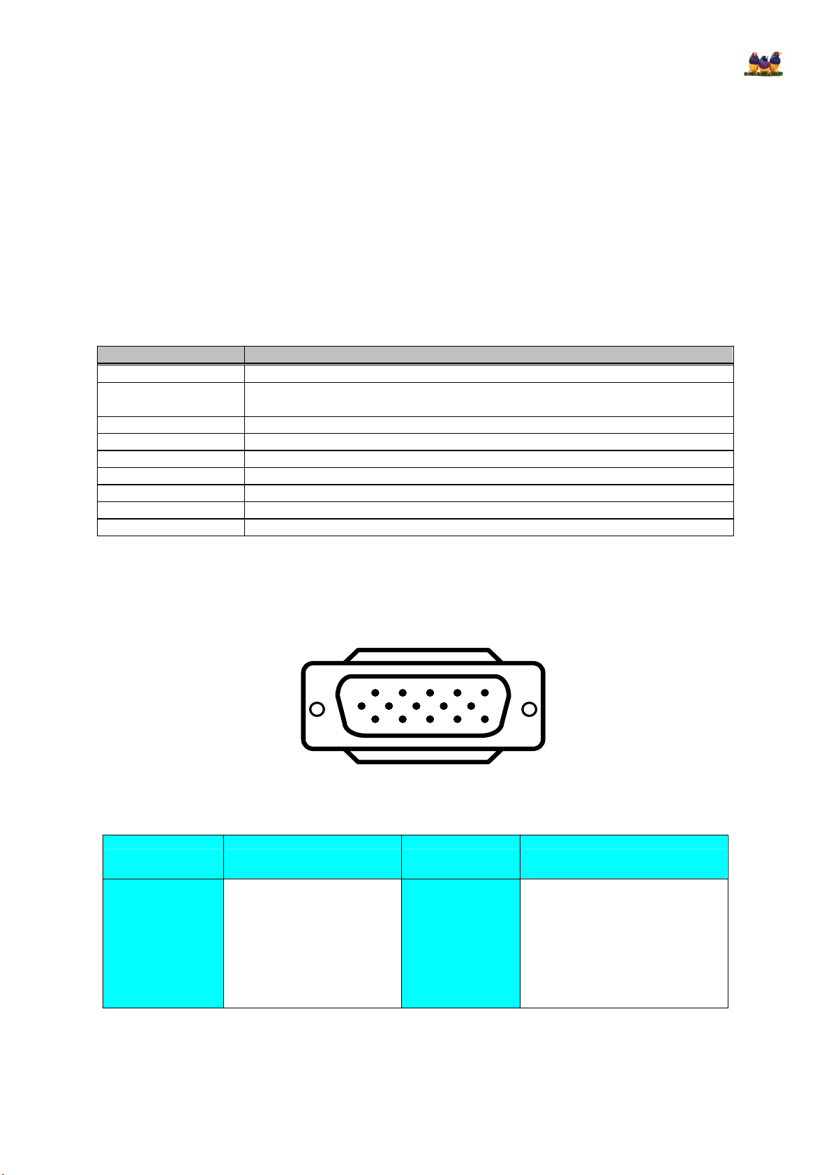
1.4 D-Sub pin distribution
Connect the 15-pin color display shielded signal cable to your signal system device and lock both screws on the connector to
ensure firm grounding. The connector information is as follow:
1
6
11 15
5
10
15 - Pin Color Display Signal Cable
PIN NO. DESCRIPTION PIN NO. DESCRIPTION
1. RED Video 9. NC
2. GREEN Video 10. Sync Ground
3. BLUE Video 11. RXD (for ISP)
4. TXD (for ISP) 12. Serial Data for DDC
5. Ground 13. HORIZ. SYNC
6. Ground-R 14. VERT. SYNC
7. Ground-G 15. Serial Clock for DDC
8. Ground-B
ViewSonic Corporation N1750w
7
Page 8
1.5 Factory preset display modes
Horizontal Vertical
Mode Resolution
VESA VGA
SVGA
VESA XGA 1024x768 48.4 60
MAC16” 832x624 49.725 74.55
MAC19” 1024x768 60.24 75
SVGA CVT 1280x768 47.8 60
640x480 31.5 60
640x480 37.9 72
640x480 37.5 75
720x400 31.5 70
800x600 37.9 60
800x600 48.1 72
800x600 46.9 75
Nominal Frequency
(KHz)
Nominal Frequency
(Hz)
2. Theory of operation
This section describes the operation theory of the N1750W LCD TV.
2.1 Video
“Analog Device” AD9883 shall provide analog to digital converter for this product. Video decoder shall be provided by
“Micronas” with a model number of VPC3230, and the de-interlace of this product shall be provided by “Sunplus” with a Model
Number of SPV302. The following tables define this product’s video specifications.
Input Parameter Specification
CVBS Characteristics:
Video Amplitude Signal
DC Level Sync Pulse:
S-Video Characteristics:
Video Amplitude Signal
Y, Pb, Pr Characteristics:
Video Amplitude Signal
Video Bandwidth NTSC: 6 MHz Maximum
RGB Characteristics:
Signal Type
Sync Type
Input Signal Rating
Sync Level:
Frequency Range
Pixel Color
DDC Compliance
EDID Data Table
0.7(min.) – 1.1(max.) V
Typical. 0.3 V
Y : 1.0Vp-p W / Neg. Sync (IN 75 Ω )
C : 0.285Vp-p (IN 75 Ω )
Y:1.0Vp-p (IN 75 Ω)
Pb:0.7 Vp-p(IN 75 Ω),Pr:0.7 Vp-p (IN 75 Ω)
Analog VGA
TTL, Separate Sync, with 4.7KΩ pull-down resistors
1250mV Max without damage to the product, 0-700 mV Full Range
2.5-5.25 V
Horizontal: 31.5-61K Hz, Vertical: 60-75 Hz
16 M
DDC2B Compliant
See Appendix B
ViewSonic Corporation N1750w
8
Page 9
2.2 Audio
Audio processor of this product used a “SONY” CXA2104 audio decoder (for MTS) or “Micronas” MSP3425G (for NICAM),
and used a “YAMAHA” YDA135 audio processor amplifier. In addition, a pair of speakers shall be integrated within this
product. The audio signals of this product shall comply with the specification listed in the following table.
Parameter Specification
Tuner Input Base band Input
Speaker Power Output Max
Rating
Speaker Impedance
Line In Per Tuner Spec
Line Out
Flatness of Amplitude
Response
Total Harmonic Distortion
(Po=0.1 to 2 W, f=100Hz15KHz)
Signal to Noise:
2W at 3 % T.H.D Distortion 2W at 3% T.H.D Distortion
8 Ω 8 Ω
Max. 1Vrms
N/A N/A
3 dB ( 6KHz deviation, 40Hz to 15KHz) 3 dB (200-16 kHz)
<10% <10%
30 dB (40Hz to 15KHz) 40dB (400Hz to 20 kHz)
2.3 Electrical
The following table defines the electrical specification of this product.
ELECTRICAL SPECIFICATION
1 Power Input Voltage Range 100-240VAC +/- 10% Wide Range
2 Input Frequency Range
Input Current 1.5A @ 230VAC
3
4 Power Supply Inrush
5 Power Consumption:
6 Interference with RF and Video
7 Electromagnetic Compatibility
Power Supply Transient Immunity
8
(Supply Transients and Outage)
9 Surge Immunity Test
Power Supply Missing Cycle
10
Immunity
11 Power Supply Acoustics
Efficiency >= 70% @ full load, nominal line
12
13 Leakage Current <3.5mA @ 110VAC
Power Saving
14
15 Recovery Time < 3 sec.
Power Factor Correction Compliant with EN61000-3-2
16
47-60 Hz ±3Hz
Max in < 35A (with fully loaded power supply) at 110Vac
Shall not result in permanent failure of power supply (including blown fuse)
Normal: 70 W (Max) // Sleep: < 3W (< 3W, when Power Off)
There shall be no visible interference between power supply, RF and video
signals. This applies to all available RF channels and video modes.
This product shall adhere to the compatibility and immunity specifications in
FCC.
Able to withstand an ANSI / IEEE C62.41 – 1980 6000V 200A ring wave
with no damage.
Able to withstand 1.5X nominal Line Voltage for one cycle with no damage.
Function properly without reset or visible screen artifact when ½ cycle of AC
Power is randomly missing.
The Power Supply shall not produce audible noise that would be detectable
by the user (Excluding Power Supply Fan).
“Audible” shall be defined in accordance with ISO 7779 (DIN
EN27779:1991).
Power Switch noise shall be Excluded.
When system is “OFF”, some minimal (<5W) power shall be consumed.
ViewSonic Corporation N1750w
9
Page 10
3. Adjustment
3.1 Front panel adjustment
The following front panel adjustments are available for N1750W.
POWER switch: This switch shall be visible and accessible on the down right side of front PC frame. Soft Power Switch
(TURN ON SYSTEM) and one push of Soft-Power Switch shall turn on the system.
Note: This switch is not considered the “Mains Disconnection Device” for agency purposes. The AC switch in back cover
of product can also disconnect power. The power cord is the main disconnection device.
Power Indicator LED: This LED will illuminate “Green” light when the product is ON and “Red” light when the product in
stand-by mode.
CH +/-: These two switches shall be visible and accessible on the bottom of front panel control keys. While TV/CATV is
selected as input source, activation of these keys will cycle through all available TV/CATV channels. While OSD menu is
up, activation of these keys will highlight each available adjustment. The activation time for this switch includes Press and
Hold should be less than half second.
VOL +/-: These two switches shall be visible and accessible on the bottom of front panel control keys. Activation will
increase /decrease loudness of the audio output. In addition, while OSD menu is up, activation of these keys will regulate a
pre-selected adjustment. The activation time for this switch includes Press and Hold should be less than half second.
MENU: This switch shall be visible and accessible on the left side of VOL - switches. Once pressed, this key shall bring
up the corresponding OSD menu(s) based on the selected input source.
SOURCE: This switch shall be visible and accessible on the right side of VOL + switches. Once pressed, this key shall
toggle in a closed loop of the input source selection from TV, AV1, AV2, S-Video, Component, PC
Headphone: This connector is designed purpose to use headphone. Once the headphone connected, then the speakers will
auto mute on audio output.
3.2 How to use the menu
1. Press the MENU button to display each menu
2. Use the cursor up/down to select a menu item.
3. Use the cursor left/right to enter a submenu or enable/disable the function.
4. Press the MENU button to exit the menu.
OSD Table for N1750W
Items Description
Brightness Adjust the Black levels from 0 to 100
Contrast Adjust the White levels from 0 to 100
Saturation Adjust the color from light to heavy
Tint Adjust from Red to Green
Sharpness Adjust the Sharpness levels from 0 to 10
Black Level Adjust the Black light from 0 to 100
Volume Adjust the Volume levels from 0 to 100
Treble Adjust the Hi Frequency from light to heavy
Bass Adjust the Low Frequency from light to heavy
W / Head Phone No function at this model
SRS Enable SRS or disable SRS
Caption Selections Close Caption on or off .
Mode Selection Caption or Text for C.C
Channel Selections CC1 or CC2 or Text1 or Text2
Display Selection display Box or shadow for C.C
V-Chip V-Chip relative setting
Status Setting V-Chip function enable or disable
TV Guidelines TV Guidelines Setting
Movie Guidelines Movie Guidelines Setting
Change Pin Change Pin for V-Chip control
Sleep Timer Setting time to auto turn TV off
Set Up Setting TV basic function
TV / VIDEO MODE
ViewSonic Corporation N1750w
10
Page 11
Blue Screen Sets Blue Screen on or off
Language Selections English, Spanish or French
Air / Cable Selections Air TV input or Cable TV input
Ch. Search Channel auto search by TV set
CH. Del ‹ Add › Skip or add current channel
View Mode Select view mode at 4:3 or 16:9 or non-Linear
Reset Reset TV to default value
PC
Brightness Adjust the Black levels from 0 to 100
Contrast Adjust the White levels from 0 to 100
Focus Adjust the color from light to heavy
H Position Adjust screen horizontal position
V Position Adjust screen vertical position
Auto Fine tuning clock and phase
Volume Adjust the Volume levels from 0 to 100
Treble Adjust the Hi Frequency from light to heavy
Bass Adjust the Low Frequency from light to heavy
SRS Enable SRS or disable SRS
Language Selections English, Spanish or French
PIP Select PIP relative function.
Position Adjust Sub-screen position
Source Selections Sub-screen display TV or AV1 or AV2 or S-Video
Audio Select Select audio from main-screen or sub-screen
Warm Setting color Temp. warm
Cool Setting color Temp. cool
Clock Adjust PC display clock for better performance
Caption Selections Close Caption on or off .
Mode Selection Caption or Text for C.C
Channel Selections CC1 or CC2 or Text1 or Text2
Display Selection display Box or shadow for C.C
Red Setting color Temp. more red.
Green Setting color Temp. more green.
Blue Setting color Temp. more blue.
Color Color Temp. Relative setting
V-Chip V-Chip relative setting f
Status Setting V-Chip function enable or disable
TV Guidelines TV Guidelines Setting
Movie Guidelines Movie Guidelines Setting
Change Pin Change Pin for V-Chip control
ViewSonic Corporation N1750w
11
Page 12
4. Assembly and disassembly procedure
This section covers disassembly and reassembly of the N1750W LCD TV. Removal of external casing, its individual parts or
internal components can render the product dangerous. There can be a risk of electric shock from exposed components even when
the device is not connected to a power source.
4.1 Disassembly
1. Remove the cover rear as arrow direction
2. Unscrew and remove eleven screws marked red.
3. Remove the back rear.
For a screw under
the base
ViewSonic Corporation N1750w
12
Page 13
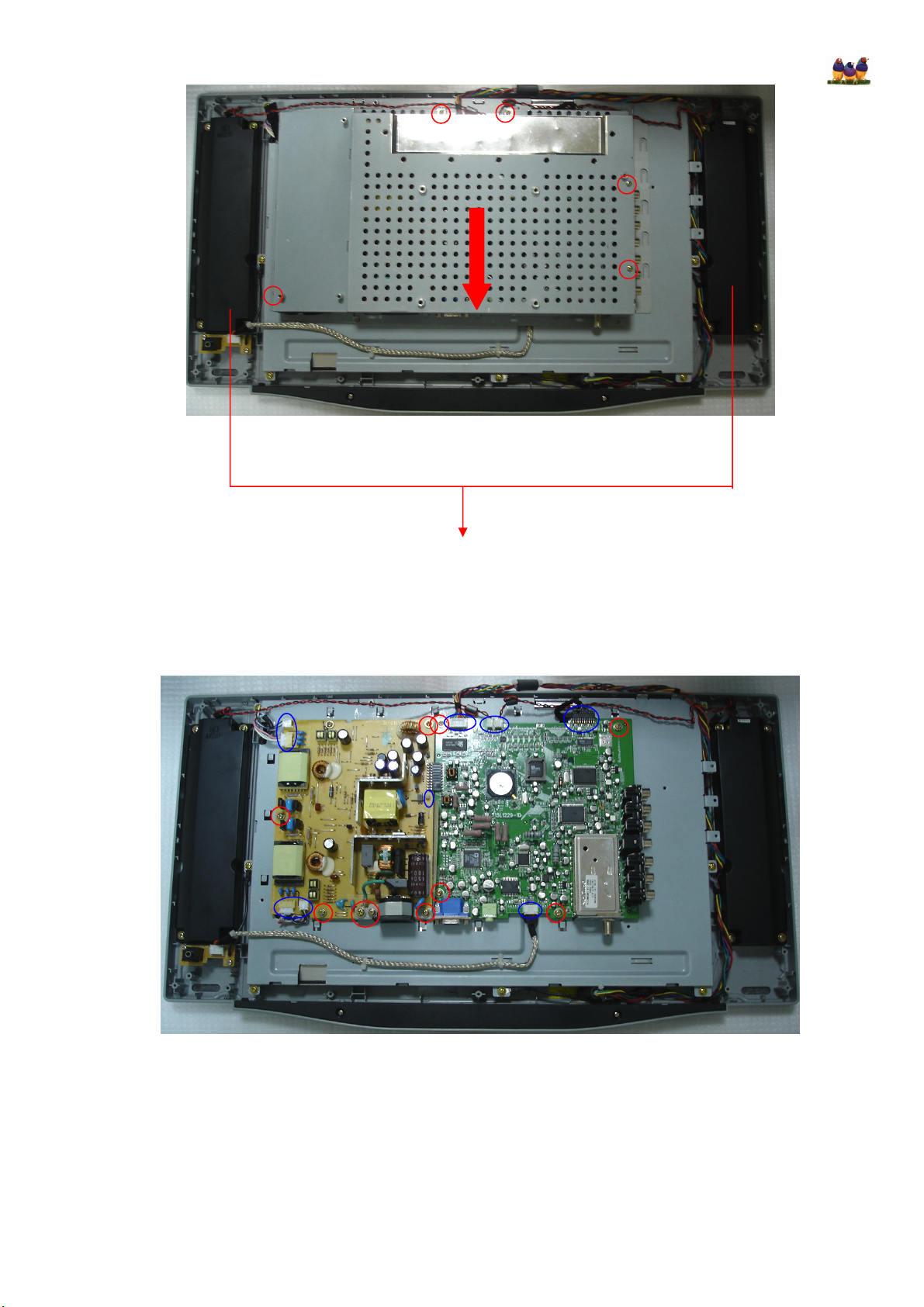
4. Unscrew and remove four screws marked red.
5. Remove the shield as arrow direction.
Two speakers
6. Unscrew and remove six screws marked red in power board.
7. Remove the connector wire marked blue in power board.
8. Unscrew and remove four screws marked red in main board.
9. Remove the connector wire marked blue in main board.
10. Remove the power board and main board synchronously
ViewSonic Corporation N1750w
13
Page 14
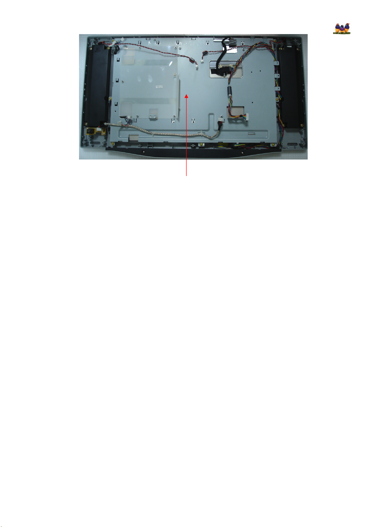
LCD Panel
ViewSonic Corporation N1750w
14
Page 15
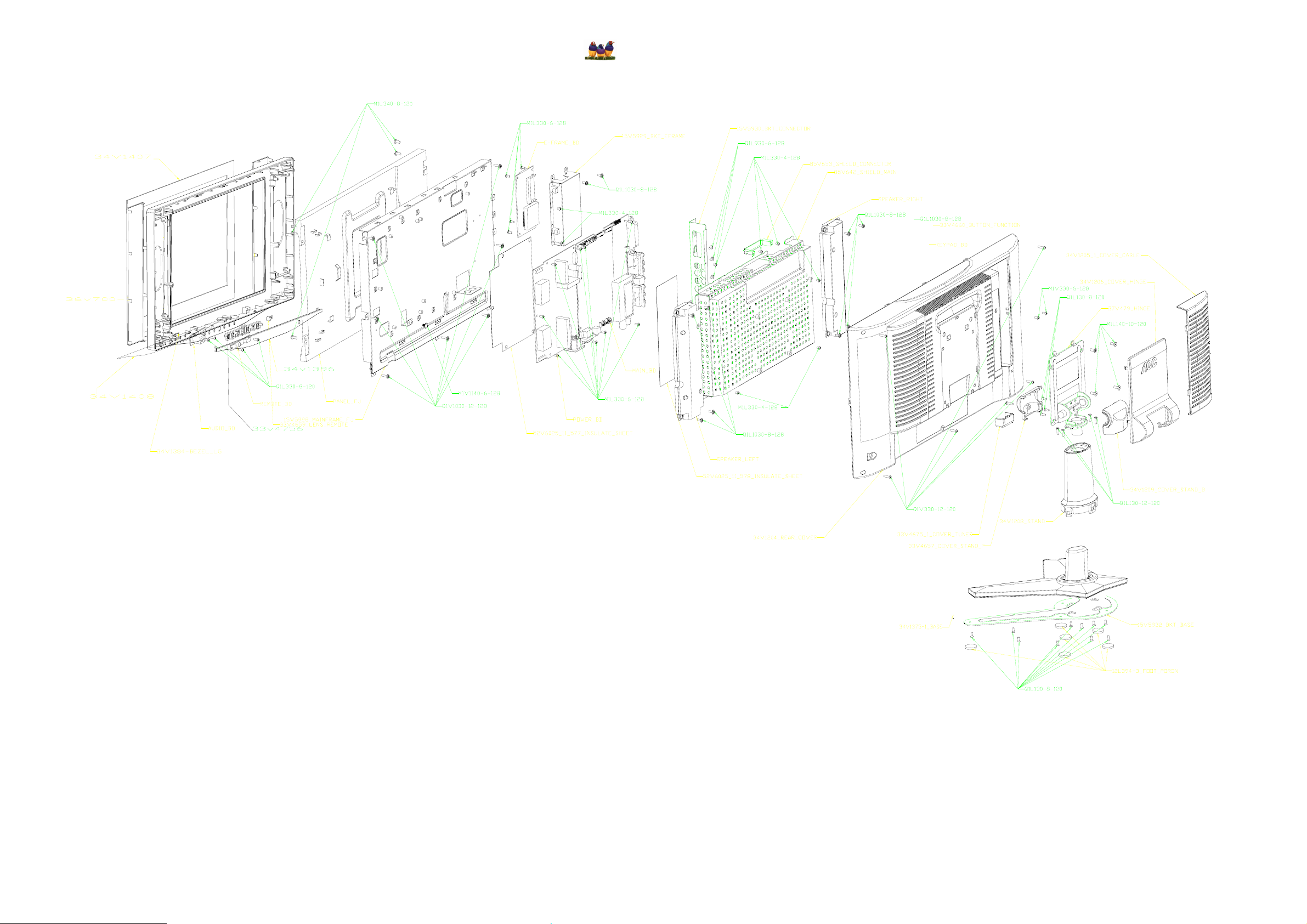
5. Exploded view
ViewSonic Corporation N1750w
15
Page 16

6. PCB Layout
6.1 Main board
ViewSonic Corporation N1750w
16
Page 17

6.2 Power board
ViewSonic Corporation N1750w
17
Page 18

7. Main board IC descriptions
g
r
g
r
7.1 SPV302A
7.1.1 General Description
The SPV302A is a highly integrated processor solution for multi-media LCD/CRT TV applications. It is a dual source device
with input sources from D-sub. This chip provides 3D motion adaptive de-interlacing, 2:2/3:2 film mode detection, video PIP/POP,
SDRAM controller, color controls, OSD and embedded CPU. In addition to being a complete solution for multi-media LCD/CRT
TV applications, the SPV302A also has the full service and support of Sunplus.
7.1.2 Block diagram
Port A
Port B
Port C
Sync
signals
YUV/RGB
interface
Sync
Processor
SDRAM/SGRAM
main
sub
DRAM
controller
DMA
controller
Timing
Generator
Video mode
Graphic mode
Auto
Calibration
deinterlace
Scaling up/down
CPU
Flash ROM
engine
De-interlaced
timing
enerato
Display
timing
enerato
Skin/Gain/
Offset
Gamma
table/Dithering
Display timing
OSD MUX
OSD engine
output
ViewSonic Corporation N1750w
18
Page 19

7.1.3 List of pins and package
388-pin PBGA
A
B
C
D
E
F
G
H
J
K
L
M
N
P
R
T
U
V
W
Y
AA
AB
AC
AD
AE
AF
Signal Description
Ball Pin Name Dir. Description Memo
AF13 MPLLVDD25 PG MPLL power (2.5V)
AF14 MPLLVSS25 PG MPLL ground
D7 OPLLVDD25 PG OPLL power (2.5V)
B6 OPLLVSS25 PG OPLL ground
B5 DPLLVDD25 PG DPLL power (2.5V)
D6 DPLLVSS25 PG DPLL ground
A4 UPLLVDD25 PG USB PLL power 2.5v
C6 UPLLVSS25 PG USB PLL ground
E1 XTALI I Crystal pad input (12MHz)
F2 XTALO O Crystal pad output
C4 RVDD33 PG RTC crystal pad input 3.3V
D3 XTALIRTC I 32768 crystal pad input
E3 XTALORTC O 32768 crystal pad output
B3 RVSS33 PG RTC crystal pad ground
A3 ADCVSS33 PG Key-scan ADC analog ground
C5 ADC0 Channel 0 input
D5 ADC1 Channel 1 input
B4 ADCVDD33 PG Key-scan ADC analog power 3.3V
If built-in USB transceiver is disabled, the SPV302A must
S
np
u
us
l
A
r
o
Clock Interface
Key-Scan ADC Interface
USB Interface
o
C
C
O
n
U
i
f
S
n
de
O
E
a
i
t
N
l
Y
L
Double
bound
Double
bound
Double
bound
Double
bound
Double
bound
Double
bound
ViewSonic Corporation N1750w
19
Page 20

communicate with an external USB transceiver. Whether to use an
internal or an external USB transceiver is determined by an IO-trap.
If the external transceiver is selected, pins FM30-FM35 serve as the
interface connection to the external USB transceiver
E4 UVDD33 PG USB transceiver analog power
C2 DP B USB data plus
D2 DM B USB data minus
D1 UVSS33 PG USB transceiver analog ground
CPU Interface
H4 P10 B
F1 P11 B
G3 P12 B
G2 P13 B
J4 P14 B
G1 P15 B
H3 P16 B
H2 P17 B
F3 HWRST I Power on reset, active high D,S
J3 P00 B CPU port 0, address/data multiplex pin, bit 0 U,S
H1 P01 B CPU port 0, address/data multiplex pin, bit1 U,S
L3 P02 B CPU port 0, address/data multiplex pin, bit 2 U,S
J1 P03 B CPU port 0, address/data multiplex pin, bit 3 U,S
K3 P04 B CPU port 0, address/data multiplex pin, bit 4 U,S
J2 P05 B CPU port 0, address/data multiplex pin, bit 5 U,S
K2 P06 B CPU port 0, address/data multiplex pin, bit6 U,S
K1 P07 B CPU port 0, address/data multiplex pin, bit 7 U,S
L2 P20 B
L1 P21 B CPU port2, high byte address, bit1 U,S
M1 P22 B CPU port2, high byte address, bit2 U,S
M3 P23 B CPU port2, high byte address, bit3 U,S
M2 P24 B CPU port2, high byte address, bit4 U,S
N1 P25 B CPU port2, high byte address, bit5 U,S
N2 P26 B CPU port2, high byte address, bit6 U,S
N3 P27 B CPU port2, high byte address, bit7 U,S
Default function Alternative function
Default
function
General
purpose
IO1, bit0
(trap0)
General
purpose
IO1, bit1
(trap1)
General
purpose
IO1, bit2
(trap2)
General
purpose
IO1, bit3
(trap3)
General
purpose
IO1, bit4
(trap4)
General
purpose
IO1, bit5
(trap5)
General
purpose
IO1, bit6
(trap6)
General
purpose
IO1, bit7
(trap7)
CPU port 2, high byte address, bit0. This bus is an output bus in the
internal CPU mode and an input bus in the external CPU mode
Alternative
function
CPU port 1, bit0 EOSDEN (I) Probe 0 S
CPU port 1, bit1 EOSDB(I) Probe 1 S
CPU port 1, bit2 EOSDG(I) Probe 2 S
CPU port 1, bit3 EOSDR(I) Probe 3 S
CPU port 1, bit4
CPU port 1, bit5
CPU port 1, bit6 PWM1/ (O) Probe 6 S
CPU port 1, bit7 PWM0/ (O) Probe 7 S
Alternative
function
PWM3/
Backlight
power(O)
PWM2/ Panel
power(O)
Alternative
function
Probe 4 S
Probe 5 S
U,S
ViewSonic Corporation N1750w
20
Page 21

P1 P30 B CPU port3, bit0. (RXD) General purpose IO3 bit0 U,S
P2 P31 B CPU port3, bit1. (TXD) General purpose IO3 bit1 U,S
P3 P32 B CPU port3, bit2. (INT0nn) General purpose IO3 bit2 U,S
P4 P33 B CPU port3, bit3 General purpose IO3 bit3 U,S
R1 P34 B CPU port3, bit4. (T0) General purpose IO3 bit4 U,S
R2 P35 B CPU port3, bit5. (T1) General purpose IO3 bit5 U,S
R3 P36 B CPU port3, bit6. (WRnn) General purpose IO3 bit6 U,S
R4 P37 B CPU port3, bit7. (RDnn) General purpose IO3 bit7 U,S
Adress latch enable. This pin is an
F4 ALE B
G4 PSEN B
T1 TESTMODE I D
T2 TVREMOTE I D
AC21 EXTMCLK I D
A5 EXTDCLK I D
E2 EOSDCLK B
AE3 PRMA0 O CPU low byte address bit0 Probe 8
AC7 PRMA1 O CPU low byte address bit1 Probe 9
AD5 PRMA2 O CPU low byte address bit2 Probe 10
AD7 PRMA3 O CPU low byte address bit3 Probe 11
AF3 PRMA4 O CPU low byte address bit4 Probe 12
AD6 PRMA5 O CPU low byte address bit5 Probe 13
AE4 PRMA6 O CPU low byte address bit6 Probe 14
AF4 PRMA7 O CPU low byte address bit7 Probe15
AE5 PRMA16 O CPU extended ROM address, bit 16
AF5 PRMA17 O CPU extended ROM address, bit 17
AE6 PRMA18 O CPU extended ROM address, bit 18
AF6 ROMWRNN O
TVOUT TCON
U1 VOUT0 B B2 B0 OB0 OB0 R,8
T3 VOUT1 B B3 B1 OB1 OB1 R,8
U2 VOUT2 B B4 B2 B0 OB2 OB0 OB2 R,8
U3 VOUT3 B B5 B3 B1 OB3 OB1 OB3 R,8
V1 VOUT4 B B6 B4 B2 OB4 OB2 OB4 R,8
V2 VOUT5 B B7 B5 B3 OB5 OB3 OB5 R,8
V3 VOUT6 B B8 B6 B4 OB6 OB4 OB6 R,8
W1 VOUT7 B B9 B7 B5 OB7 OB5 OB7 R,8
Y1 VOUT8 B G2 G0 OG0 OG0 R,8
W2 VOUT9 B G3 G1 OG1 OG1 R,8
W3 VOUT10 B G4 G2 G0 OG2 OG0 OG2 R,8
W4 VOUT11 B G5 G3 G1 OG3 OG1 OG3 R,8
Y2 VOUT12 B G6 G4 G2 OG4 OG2 OG4 R,8
Y3 VOUT13 B G7 G5 G3 OG5 OG3 OG5 R,8
AA1 VOUT14 B G8 G6 G4 OG6 OG4 OG6 R,8
AA2 VOUT15 B G9 G7 G5 OG7 OG5 OG7 R,8
AA3 VOUT16 B R2 R0 OR0 OR0 R,8
AB1 VOUT17 B R3 R1 OR1 OR1 R,8
ViewSonic Corporation N1750w
output pin when the built-in CPU
is enabled. When an external CPU
is used, this pin is an input pin
Program space enable. This pin is
an output pin when the built-in
CPU is enabled. When an external
CPU is used, this pin is input pin
EOSDCLK is a default to connect 2 times of display clock(i.e.,
EXTOCLKx2) for the test mode. It can be programmed to output an
internal display clock for an external OSD chip
External write pulse. This pin is used in the ISP (in-system-
programming) function
Video Output Interface
Video output interface can be routed to embedded DAC for testing.
VOUT[29:0] are routed to video DAC according to 10bit single
pixel format. VOUT]37:30] are routed to SVM DAC.
Single
pixel
10bit
Single
pixel 8bit
Single
pixel 6bit
21
SCL of I2C interface (I) S
SDA of I2C interface (B) S
Dual pixel
8bit
Dual
pixel
6bit
D
Page 22

AB2 VOUT18 B R4 R2 RO OR2 OR0 OR2 R,8
AB3 VOUT19 B R5 R3 R1 OR3 OR1 OR3 R,8
AB4 VOUT20 B R6 R4 R2 OR4 OR2 OR4 R,8
AC1 VOUT21 B R7 R5 R3 OR5 OR3 OR5 R,8
AC2 VOUT22 B R8 R6 R4 OR6 OR4 OR6 R,8
AC3 VOUT23 B R9 R7 R5 OR7 OR5 OR7 R,8
AE1 VOUT24 B B0 EB0 EB0 R,8
AD3 VOUT25 B B1 EB1 EB1 R,8
AE2 VOUT26 B G0 EB2 EB0 EB2 R,8
AC5 VOUT27 B G1 EB3 EB1 EB3 R,8
AF1 VOUT28 B R0 EB4 EB2 EB4 R,8
AD4 VOUT29 B R1 EB5 EB3 EB5 R,8
AC6 VOUT30 B EB6 EB4 EB6 R,8
AF2 VOUT31 B EB7 EB5 EB7 R,8
AD18 VOUT32 B EG0 EG0 R,8
AF19 VOUT33 B EG1 EG1 R,8
AE19 VOUT34 B EG2 ER0 EG2 R,8
AF20 VOUT35 B EG3 ER1 EG3 R,8
AD19 VOUT36 B EG4 EG2 EG4 R,8
AE20 VOUT37 B EG5 EG3 EG5 R,8
AF21 VOUT38 B EG6 EG4 EG6 R,8
AD20 VOUT39 B EG7 EG5 EG7 R,8
AE21 VOUT40 B ER0 ER0 R,8
AF22 VOUT41 B ER1 ER1 R,8
AD21 VOUT42 B ER2 ER0 ER2 R,8
AE22 VOUT43 B ER3 ER1 ER3 R,8
AF23 VOUT44 B ER4 ER2 ER4 R,8
AF24 VOUT45 B ER5 ER3 ER5 R,8
AD22 VOUT46 B ER6 ER4 ER6 R,8
AE23 VOUT47 B ER7 ER5 ER7 R,8
AD1 HSOUT O Output horizontal sync STV1 T,R,8
AD2 VSOUT O Output vertical sync STV3 T,R,8
AC4 DEN O Output data enable OE1 T,R,8
Y4 CLK1 O Output clock 1 OE2 T,R,8
AA4 CLK2 O Output 2 OE3 T,R,8
Video DAC Interface
AE7 AVDD33 PG Video DAC Analog power 3.3V
AD8 AVDD33 PG Video DAC Analog power 3.3V
AE8 AVDD33 PG Video DAC Analog power 3.3V
AF7 AROUT DAC analog red/Y output
AF9 AGOUT DAC analog green/Pb output
AF10 ABOUT DAC analog blue/ Pr output
AE9 CBU Connect to power via a 0.1 UF capacitor
AD10 CBL Connect to power via a 0.1 UF capacitor
AD9 RSET DAC scale adjustment
AF8 VREF DAC voltage reference
AE10 AVSS33 PG Video DAC Analog ground
AD11 AVSS33 PG Video DAC Analog ground
AE11 AVSS33 PG Video DAC Analog ground
AE12 AVSS33 PG Video DAC Analog ground
AE13 SVMOUT SVM output
AD13 VMCBU Connect to power via a 0.1UF capacitor
AC13 VMCBL Connect to power via a 0.1UF capacitor
AF12 VMREF DAC scale adjustment
AF11 VMREF DAC voltage reference
AD12 AVDD33 PG SVM DAC Analog power 3.3V
General Purpose I/O power
A23 FM1 B GPIO
A22 FM2 B GPIO
A21 FM4 B GPIO
A20 FM5 B GPIO
ViewSonic Corporation N1750w
22
Page 23

C20 FM6 B GPIO
B20 FM7 B GPIO
C19 FM8 B GPIO
A19 FM9 B GPIO
B19 FM10 B GPIO
C18 FM11 B GPIO
B18 FM12 B GPIO
A18 FM13 B GPIO
A17 FM14 B GPIO
C17 FM15 B GPIO
B17 FM16 B GPIO
A16 FM17 B GPIO
B16 FM18 B GPIO
A15 FM20 B GPIO
B15 FM21 B GPIO
C15 FM22 B GPIO
A14 FM23 B GPIO
B14 FM24 B GPIO
AC14 FM25 B GPIO
AE14 FM26 B GPIO
AD14 FM27 B GPIO
AF15 FM28 B GPIO
AE15 FM29 B GPIO
AD15 FM30 B GPIO
AF16 FM31 B GPIO
AE16 FM32 B GPIO
AD16 FM33 B GPIO
AF17 FM34 B GPIO
AE17 FM35 B GPIO
AD17 FM36 B GPIO
AF18 FM37 B GPIO
AE18 FM38 B GPIO
SDRAM Interface
AF25 MD0 B SDRAM data bus, bit0 R,8
AC22 MD1 B SDRAM data bus, bit1 R,8
AD23 MD2 B SDRAM data bus, bit2 R,8
AF26 MD3 B SDRAM data bus, bit3 R,8
AE24 MD4 B SDRAM data bus, bit4 R,8
AC23 MD5 B SDRAM data bus, bit5 R,8
AD24 MD6 B SDRAM data bus, bit6 R,8
AE25 MD7 B SDRAM data bus, bit7 R,8
AB24 MD8 B SDRAM data bus, bit8 R,8
AC25 MD9 B SDRAM data bus, bit9 R,8
AD26 MD10 B SDRAM data bus, bit10 R,8
AA24 MD11 B SDRAM data bus, bit11 R,8
AB25 MD12 B SDRAM data bus, bit12 R,8
AC26 MD13 B SDRAM data bus, bit13 R,8
AB26 MD14 B SDRAM data bus, bit14 R,8
Y24 MD15 B SDRAM data bus, bit15 R,8
W23 MD16 B SDRAM data bus, bit16 D,R,8
AA25 MD17 B SDRAM data bus, bit17 D,R,8
AA26 MD18 B SDRAM data bus, bit18 D,R,8
Y25 MD19 B SDRAM data bus, bit19 D,R,8
W24 MD20 B SDRAM data bus, bit20 D,R,8
Y26 MD21 B SDRAM data bus, bit21 D,R,8
W25 MD22 B SDRAM data bus, bit22 D,R,8
V24 MD23 B SDRAM data bus, bit23 D,R,8
W26 MD24 B SDRAM data bus, bit24 D,R,8
V25 MD25 B SDRAM data bus, bit25 D,R,8
U24 MD26 B SDRAM data bus, bit26 D,R,8
V26 MD27 B SDRAM data bus, bit27 D,R,8
ViewSonic Corporation N1750w
23
Page 24

U25 MD28 B SDRAM data bus, bit28 D,R,8
U26 MD29 B SDRAM data bus, bit29 D,R,8
T24 MD30 B SDRAM data bus, bit30 D,R,8
T25 MD31 B SDRAM data bus, bit10 D,R,8
N24 DQM0L O SDRAM data mask signal, bank0, low byte R,8
M26 DQM0H O SDRAM data mask signal, bank0, high byte R,8
M25 DQM1L O SDRAM data mask signal, bank1, low byte R,8
M24 DQM1H O SDRAM data mask signal, bank1, high byte R,8
AC24 WENN O SDRAM write enable signal R,8
AB23 SDCLK O SDRAM clock R,8
AD25 RASNN O SDRAM raw address strobe signal R,8
AE26 CASNN O SDRAM column address strobe signal R,8
L26 MA0 O SDRAM address bus, bit0 R,8
L25 MA1 O SDRAM address bus, bit1 R,8
L24 MA2 O SDRAM address bus, bit2 R,8
K26 MA3 O SDRAM address bus, bit3 R,8
K25 MA4 O SDRAM address bus, bit4 R,8
K24 MA5 O SDRAM address bus, bit5 R,8
J26 MA6 O SDRAM address bus, bit6 R,8
J25 MA7 O SDRAM address bus, bit7 R,8
H26 MA8 O SDRAM address bus, bit8 R,8
H25 MA9 O SDRAM address bus, bit9 R,8
J24 MA10 O SDRAM address bus, bit10 R,8
J23 MA11 O SDRAM address bus, bit11 R,8
G26 MA12 O SDRAM address bus, bit12 R,8
H24 MA13 O SDRAM address bus, bit13 R,8
H23 MA14 O SDRAM address bus, bit14 R,8
Video Input Interface
The SPV302A supports three video interfaces, port A, port B and
T26 CLKC B CLKC (I) CPV (O) D,R,8
R25 DATAC0 B DATAC0 (I) CPH (O) D,R,8
R24 DATAC1 B DATAC1 (I) STH1 (O) D,R,8
R26 DATAC2 B DATAC2 (I) RLS (O) D,R,8
P24 DATAC3 B DATAC3 (I) LP (O) D,R,8
P25 DATAC4 B DATAC4 (I) POL (O) D,R,8
P26 DATAC5 B DATAC5 (I) SHC (O) D,R,8
N26 DATAC6 B DATAC6 (I) INV1 (O) D,R,8
N25 DATAC7 B DATAC7 (I) INV2 (O) D,R,8
YUV RGB(888)
F26 DATAA0 I UV0 R0 RA0
G25 DATAA1 I UV1 R1 RA1
G24 DATAA2 I UV2 R2 RA2
F25 DATAA3 I UV3 R3 RA3
E26 DATAA4 I V6/4/2/0 UV4 R4 RA4
G23 DATAA5 I V7/5/3/1 UV5 R5 RA5
F24 DATAA6 I U6/4/2/0 UV6 R6 RA6
E25 DATAA7 I U7/5/3/1 UV7 R7 RA7
D26 DATAA8 I DA0 YUV0 Y0 Y0 G0 GA0
F23 DATAA9 I DA1 YUV1 Y1 Y1 G1 GA1
E24 DATAA10 I DA2 YUV2 Y2 Y2 G2 GA2
D25 DATAA11 I DA3 YUV3 Y3 Y3 G3 GA3
C26 DATAA12 I DA4 YUV4 Y4 Y4 G4 GA4
E23 DATAA13 I DA5 YUV5 Y5 Y5 G5 GA5
D24 DATAA14 I DA6 YUV6 Y6 Y6 G6 GA6
port C. When the TCON interface is disabled, port C is used to
connect a video decoder in CCIR656 format. When the TCON
interface is enabled, port C is used to output TCON control signals.
8bit
(656)
422
format
8bit (601) 12bit 16bit 24bit 48bit
422 format 411 format 422 format
Single
pixel
Dual
pixel
ViewSonic Corporation N1750w
24
Page 25

C25 DATAA15 I DA7 YUV7 Y7 Y7 G7 GA7
B26 DATAA16 I B0 BA0
D23 DATAA17 I B1 BA1
B25 DATAA18 I B2 BA2
A26 DATAA19 I VREFA VREFA VREFA B3 BA3
D22 DATAA20 I FIELDA FIELDA FIELDA B4 BA4
C24 DATAA21 I B5 BA5
D21 DATAA22 I HREFA HREFA HREFA B6 BA6
C23 DATAA23 I DVALIDA DVALIDA DVALIDA B7 BA7
C14 DATAB0 I UV0 RB0
A13 DATAB1 I UV1 RB1
B13 DATAB2 I UV2 RB2
C13 DATAB3 I UV3 RB3
A12 DATAB4 I V6/4/2/0 UV4 RB4
B12 DATAB5 I V7/5/3/1 UV5 RB5
C12 DATAB6 I U6/4/2/0 UV6 RB6
A11 DATAB7 I U7/5/3/1 UV7 RB7
B11 DATAB8 I DA0 YUV0 Y0 Y0 GB0
C11 DATAB9 I DA1 YUV1 Y1 Y1 GB1
A10 DATAB10 I DA2 YUV2 Y2 Y2 GB2
B10 DATAB11 I DA3 YUV3 Y3 Y3 GB3
C10 DATAB12 I DA4 YUV4 Y4 Y4 GB4
A9 DATAB13 I DA5 YUV5 Y5 Y5 GB5
B9 DATAB14 I DA6 YUV6 Y6 Y6 GB6
C9 DATAB15 I DA7 YUV7 Y7 Y7 GB7
A8 DATAB16 I BB0
B8 DATAB17 B VSB VSB VSB BB1
C8 DATAB18 I CLKB CLKB CLKB BB2
A7 DATAB19 I VREFB VREFB VREFB BB3
B7 DATAB20 I FIELDB FIELDB FIELDB BB4
A6 DATAB21 B HSB HSB HSB BB5
D8 DATAB22 I HREFB HREFB HREFB BB6
C7 DATAB23 I DVALIDB DVALIDB DVALIDB BB7
B24 HSA B Horizontal sync of video port A S
C22 VSA B Vertical sync of video port A S
D20 CLKA I Input clock of video port A
C21 PCHS I Raw horizontal sync of video port A S
A25 CLAMP B Clamp signal for DC restoration of analog input data (trap 10)
A24 CVS B Regenerated vertical sync from composite sync (trap 8)
B23 CHS B Regenerated horizontal sync from composite sync (trap 9)
Digital IO Power Pair
A1,A2,B1,B2,C1,C3,D4,M12,M13,M14,
M15,N12,N13,N14,N15,P12,P13,P14,
P15,R12
AA23,AC9,AC10,AC18,AC19,AC20,
D12,D13,D14,M4,M23,N4,N23,P23,R23,
Y23
Digital Core Power Pair
L11,R13,R14,R15,D15,L12,L13,L14,
L15,L16,M11,M16,N11,N16,P11,P16,
R11,R16,T11,T12,T13,T14,T15,T16,
AC12,D16,T4
AC8,AC11,AC15,AC16,AC17,D9,
D10,D11,D17,D18,D19,K4,K23,L4,L23,
T23,U4,U23,V4,V23
No Connection Pins
B22,B21,C16 N.C.
DVSS33
DVDD33 3.3V
DVSS25
DVDD25 2.5V
Memo:
U: internal pull-up R: Limited slew rate output
D: internal pull-down 8: 8mA output current
S: Schmitt trigger input 16: 16mA output current
T: 3-state output
ViewSonic Corporation N1750w
25
Page 26

7.1.4 IO-Trap
While most configurations of the SPV302A can be programmed by firmware, there are some configurations that must be
determined immediately after the chip is powered-on. The SPV302A adopts an IO-trap mechanism to set these configurations. These
configurations are not changed during the operation of the SPV302A. The SPV302A samples signal states on the video output bus
when the reset signal goes form high to low. These samples values, in turn, set the internal configurations. The following table lists all
the IO-trap values in the SPV302A:
Name Description Note
Trap[0] Extcpu
Trap[1] Fastrsten
Trap[2] MPU_I2C
Trap[4:3] I2Cslave
Trap[5] Extusb 1’b1
Trap[6] Extflash
Trap[7] Lvrsten
Trap[9:8] Lvdelay
Trap[10]
0: use internal CPU
1: use external CPU (or ICE)
0: Normal mode (10 ms reset)
1: Fast reset (32 xtal clock)
Use external CPU interface
0: use serial I2C interface
1: use parallel MPU interface
Set I2C alave address
00: 68H 01: 6AH
10: 6CH 11: 6EH
0: executes internal ROM code
1: executes external ROM code
0: disables low voltage reset
1: enable low voltage reset
Configures low voltage detector response time
00: delay 64 xtal clocks
01: delay 128 xtal clocks
10: delay 256 xtal clocks
11: delay 512 xtal clocks
0: set video output interface to VOUT port
1: set parallel MPU interface to VOUT port
ViewSonic Corporation N1750w
26
Page 27

7.2 AD9883
7.2.1 Description
The AD9883A is a complete 8-bit, 140 MSPS monolithic analog interface optimized for capturing RGB graphics signals from
personal computers and workstations. Its 140 MSPS encode rate capability and full power analog bandwidth of 300 MHz supports
resolutions up to SXGA (1280 x 1024 at 75Hz).
7.2.2 Block diagram
ViewSonic Corporation N1750w
27
Page 28

7.3 VPC3230D
7.3.1 Description
The VPC 323xD/324xD is a high-quality, single-chip Multi-standard color decoder which is targeted for 4:3 and 16:9, 50/60 and
100/120 Hz TV sets. it integrates 4H comb filter Y/C separator, high-quality A/D converter, multi-type scaler, multi-outputs
formats interfaces ,high-quality soft mixer and I square C bus interface. It can supports PIP which can be processed in 15
predefined positions and provides linear horizontal scaling and non-linear scaling for different purposes. It only take few
peripheral components and a 20.25 MHz crystal and the package of it is 80-pin PQFP.
7.3.2 Block diagram
7.3.3 Pin functions
Pin No.
PQFP
80-pin
1 B1/CB1IN IN VREF Blue1/Cb1 Analog Component Input
2 G1/Y1IN IN VREF Green1/Y1 Analog Component Input
3 R1/CR1IN IN VREF Red1/Cr1 Analog Component Input
4 B2/CB2IN IN VREF Blue2/Cb2 Analog Component Input
5 G2/Y2IN IN VREF Green2/Y2 Analog Component Input
6 R2/CR2IN IN VREF Red2/Cr2 Analog Component Input
7 ASGF X Analog Shield GNDF
8 FFRSTWIN IN LV or GNDD FIFO Reset Write Input **
9 VSUPCAP OUT X Digital Decoupling Circuitry Supply Voltage
10 VSUPD SUPPLYD X Supply Voltage, Digital Circuitry
11 GNDD SUPPLYD X Ground, Digital Circuitry
12 GNDCAP OUT X Digital Decoupling Circuitry GND
13 SCL IN/OUT X I2C Bus Clock
14 SDA IN/OUT X I2C Bus Data
15 RESQ IN X Reset Input, Active Low
16 TEST IN GNDD Test Pin, connect to GNDD
17 VGAV IN GNDD VGAV Input
18 YCOEQ IN GNDD Y/C Output Enable Input, Active Low
19 FFIE OUT LV FIFO Input Enable
20 FFWE OUT LV FIFO Write Enable
21 FFRSTW OUT LV FIFO Reset Write/Read
Pin Name Type Connection
Short Description
(if not used)
ViewSonic Corporation N1750w
28
Page 29

22 FFRE OUT LV FIFO Read Enable
23 FFOE OUT LV FIFO Output Enable
24 CLK20 IN/OUT LV Main Clock Output 20.25 MHz
25 GNDPA OUT X Pad Decoupling Circuitry GND
26 VSUPPA OUT X Pad Decoupling Circuitry Supply Voltage
27 LLC2 OUT LV Double Clock Output
28 LLC1 IN/OUT LV Clock Output
29 VSUPLLC SUPPLYD X Supply Voltage, LLC Circuitry
30 GNDLLC SUPPLYD X Ground, LLC Circuitry
31 Y7 OUT GNDY Picture Bus Luma (MSB)
32 Y6 OUT GNDY Picture Bus Luma
33 Y5 OUT GNDY Picture Bus Luma
34 Y4 OUT GNDY Picture Bus Luma
35 GNDY SUPPLYD X Ground, Luma Output Circuitry
36 VSUPY SUPPLYD X Supply Voltage, Luma Output Circuitry
37 Y3 OUT GNDY Picture Bus Luma
38 Y2 OUT GNDY Picture Bus Luma
39 Y1 OUT GNDY Picture Bus Luma
40 Y0 OUT GNDY Picture Bus Luma (LSB)
41 C7 OUT GNDC Picture Bus Chroma (MSB)
42 C6 OUT GNDC Picture Bus Chroma
43 C5 OUT GNDC Picture Bus Chroma
44 C4 OUT GNDC Picture Bus Chroma
45 VSUPC SUPPLYD X Supply Voltage, Chroma Output Circuitry
46 GNDC SUPPLYD X Ground, Chroma Output Circuitry
47 C3 OUT GNDC Picture Bus Chroma
48 C2 OUT GNDC Picture Bus Chroma
49 C1 OUT GNDC Picture Bus Chroma
50 C0 OUT GNDC Picture Bus Chroma (LSB)
51 GNDSY SUPPLYD X Ground, Sync Pad Circuitry
52 VSUPSY SUPPLYD X Supply Voltage, Sync Pad Circuitry
53 INTLC OUT LV Interlace Output
54 AVO OUT LV Active Video Output
55 FSY/HC/HSYA OUT LV Front Sync/ Horizontal Clamp Pulse/Front-End
Horizontal Sync Output **
56 MSY/HS IN/OUT LV Main Sync/Horizontal Sync Pulse
57 VS OUT LV Vertical Sync Pulse
58 FPDAT/VSYA IN/OUT LV Front-End /Back-End Data/Front-End Vertical
Sync Output **
59 VSTBY SUPPLYA X Standby Supply Voltage
60 CLK5 OUT LV CCU 5 MHz Clock Output
61 NC –
62 XTAL1 IN X Analog Crystal Input
63 XTAL2 OUT X Analog Crystal Output
64 ASGF X Analog Shield GNDF
65 GNDF SUPPLYA X Ground, Analog Front-End
66 VRT OUTPUT X Reference Voltage Top, Analog
67 I2CSEL IN X I2C Bus Address Select
68 ISGND SUPPLYA X Signal Ground for Analog Input, connect to
69 VSUPF SUPPLYA X Supply Voltage, Analog Front-End
70 VOUT OUT LV Analog Video Output
71 CIN IN LV* Chroma / Analog Video 5 Input
72 VIN1 IN VRT* Video 1 Analog Input
73 VIN2 IN VRT Video 2 Analog Input
74 VIN3 IN VRT Video 3 Analog Input
75 VIN4 IN VRT Video 4 Analog Input
76 VSUPAI SUPPLYA X Supply Voltage, Analog Component Inputs Front-
LV OR
GNDD
Not connected
GNDF
End
ViewSonic Corporation N1750w
29
Page 30

77 GNDAI SUPPLYA X Ground, Analog Component Inputs Front-End
78 VREF OUTPUT X Reference Voltage Top, Analog Component
Inputs Front-End
79 FB1IN IN VREF Fast Blank Input
80 AISGND SUPPLYA X Signal Ground for Analog Component Inputs,
connect to GNDAI
61 NC –
LV OR
GNDD
Not connected
7.4 UPD64083
7.4.1 Description
The µPD64086 realizes a high precision Y/C separation and a noise reduction by the three-dimension signal processing for
NTSC signal.
This product has the On-chip 4-Mbit memory for flame delay, 2ch of high precision internal 10-bit A/D converter, and singlechip system of 3D Y/C separation.
This LSI includes the Wide Clear Vision ID signal (Japanese local format) decoder and ID-1 signal decoder.
7.4.2 Block diagram
ViewSonic Corporation N1750w
30
Page 31

7.5 TDA7226D
7.5.1 Description
The TDA7266D is a dual bridge amplifier specially designed for LCD monitor, PC Motherboard, TV and Portable Ratio
applications
7.5.2 Block diagram
ViewSonic Corporation N1750w
31
Page 32

8. Block diagram
ANT
VIDEO 1
VIDEO 2
S-VIDEO
PHILIPS
FQ1236/F-H3
Tuner
NJM2244
Selector
17”VIEW SONIC Block Diagram
UPD64083
VPC 3230
Decoder
AT29LV040A
Flash ROM
Key PAD
IR
GTL5640L16
SDRAM
24LC16
EEPROM
17 inch
Panel
SPV302A
SCALAR
OSD
MCU
Y/Pb/Pr
D-SUB
SDA
SCL
TV_audio
D-SUB_audio
Audio 1
Audio 2
Y/Pb/Pr
PCA9554D
Selector
HCT 4052
Selector
M61323
Selector
AD 9883
MSP 3425G
AUDIO Decoder
ADC
Z86129
V-CHIP
Audio Line Out
(RCA)
PT2308
EAR AMP
AC 120 V
TDA7266D
Audio AMP
12V/5V
Inverter
POWER
Speaker (2Wx 2)
Headphone
NOTE: .AV2 and S-VIDCO USE the same Audio Input
ViewSonic Corporation N1750w
32
Page 33

9. Schematic diagram
9.1 Main board
L115
150 OHM
EMI
L118
150 OHM
PAN_PWR5,13
P_Hs6,13
P_Vs6,13
P_DATAEN6,13
P_CLK6,13
R[0..7]6,13
G[0..7]6,13
B[0..7]6,13
Comp_L10
SVIDEO_C4
SVIDEO_Y4
Comp_R10
COMP_Y2
COMP_Pb2
COMP_Pr2
L143
120 OHM
L142 120 OHM
AV_22
AV2_L2
AV2_R2
L144
C137
0.1uF
120 OHM
O_PRO_PB
O_PRO_PR
2
1
50
49
48
47
46
45
44
43
42
41
40
39
CP103 22pF
1
2
3
4
1
2
3
C130
22pF
4
J100JACK
7
1
3
5
Place near by I/O
O_PRO_Y
5
3
4
R128 75 1/16W
R129 75 1/16W
R130 75 1/16W
8
J102A
JACK
9
6
7
AGND
150 OHM
38
J105A
L128
JACK
37
36
35
8
7
6
5
CP105
8
22pF
7
6
5
AGND
L120150 OHM
AGND
34
33
R7
switch
2
1
32
R6
3
31
R5
30
R4
5
4
CN101
EAR_R10
5VP
EAR_L10
4
5
INV_PRO6
BL_ADJ5
5V
12V
3.3VM
C159
C160
CP100
22pF
12VP
+5VP
5V
8
7
6
5
120 OHM(8P4R)
R119
10K 1/16W
0.001uF
0.001uF
R117
NC
LP110
L136 600 OHM
5
6
7
8
120 OHM(8P4R)
1
2
3
4
1
2
3
16
8
1
2
3
4
5
6
CN105
CONN
VCCGND
DA
DB
DC
DD
L113 150 OHM
L114 150 OHM
L116 150 OHM
L117 150 OHM
EMI
CN106
CONN
4
7
12
9
U104
PI5V330
EMI
Remote5
KEY_AD5
3230_Y
3230_PB
3230_PR
2
1
7
8
AGND
INTERLACE_Y 4
INTERLACE_PB 4
INTERLACE_PR 4
3
6
W_ENABLE6
Audio_L+10
Audio_L-10
29
28
27
26
25
24
23
22
21
20
19
18
17
16
15
14
13
12
11
10
9
8
7
6
5
4
3
2
1
CP102
22pF
5
6
7
8
5
CP104
6
22pF
7
8
5
CP106
6
22pF
7
8
5
CP107
6
22pF
7
8
R1
R2
R3
R0
8
9
2
4
6
8
9
6
7
G4
G7
AV1_R 2
AV1_L 2
AV_1 2
G6
G5
NC
G3
L123
150 OHM
R120
G2
G1
G0
B7
Q103
B6
NC
B5
B4
AGND
R121
B3
150 OHM
150 OHM
NC
AGND
B2
L126
L127
B0
B1
Remote
Q102
NC
O_PRO_Y
O_PRO_PB
O_PRO_PR
C134
10uF/16V
C135
10uF/16V
R122
I_DVD_PR
I_DVD_PB
I_DVD_Y
DVD_AL2
DVD_AR2
+
+
NC
4
3
2
1
4
3
2
1
4
3
2
1
4
3
2
1
L138 600 OHM
AGND
5
6
7
8
120 OHM(8P4R)
L130 600 OHM
AGND
DVD_L
DVD_R
L133 600 OHM
RN105
NC
1
2
3
4
LINE_O_L 11
LINE_O_R 11
MUTE
6,10
LP107
8
7
6
5
COMP_SEL5
4
3
2
1
L131
150 OHM
3230_Y
3230_PB
3230_PR
O_PRO_Y
I_DVD_Y
O_PRO_PB
I_DVD_PB
O_PRO_PR
I_DVD_PR
Audio_R+10
Audio_R-10
AGND
L132150 OHM
C139
100pF
C140
100pF
2
3
5
6
14
13
11
10
1
15
C142
100pF
100pF
S1A
S2A
S1B
S2B
S1C
S2C
S1D
S2D
IN
/EN
100pF
C138
C141
5V
AGND
3
2
1
2
1
R118
10K 1/16W
C131
22pF
AGND
LP108
4
3
2
1
C136
0.1uF
C1560.001uF
C1550.001uF
CONN
CONN
L137
600 OHM
C132
22pF
C1580.001uF
C1540.001uF
CN111
CN112
C1570.001uF
C1430.1uF
C145
0.1uF
10
AGND
C1440.1uF
CN102
1
2
3
4
5
6
7
8
9
CONN
1
2
3
4
5
6
7
8
6
5
4
3
2
1
CN107
CONN
CN103
CONN
ViewSonic Corporation N1750w
33
Page 34

SEL1
SEL2
0
AGND
C112
C111
22pF
22pF
AV_11
AV_21
TUNER_OUT3
CH_SEL36
CH_SEL26
AV1_R_1
AV2_R_1
Comp_R_110
DVD_AR1
AV1_L_1
AV2_L_1
Comp_L_110
DVD_AL1
CH_SEL16
CH_SEL26
5V
C124
10uF/16V
12VS
+
R125
10 2W
R108
75 1/16W
C113
22pF
U100
12
X0
14
X1
15
X2
11
X3
1
Y0
5
Y1
2
Y2
4
Y3
10
A
9
B
6
EN
7
VEE
16
VDD
+
R109
75 1/16W
13
X
3
Y
GND
74HC4052D
8
U105
3 2
VI VO
C164
10uF/16V
1
GND
+
+
+
C114
10uF/16V
C116
10uF/16V
C117
10uF/16V
5V_MUX
0
0
1
0
1
1
1
5V
AGND
ASEL_O_R 11
ASEL_O_L 11
VGA_HS9
VGA_VS9
COMP_Pr1
COMP_Y1
COMP_Pb1
VIDEO_SEL6
+
C168
10uF/16V
C163
0.1uF
SEL3
0
1
1
1
C121
0.1uF
VGA_G9
VGA_B9
1
3
5
2
4
6
VGA_R9
audio
AV1
SCART
PC
SVIDEO
U102
VIN1
VIN2
VIN3
SW1
SW2
V+
video
AV1
SCART
TUNER
VOUT
GND
NJM2244
8
R114 75 1/16W
R115 75 1/16W R111 75 1/16W
7
5V_MUX
Ri
Gi
Bi
Hi
Vi
Pr
Y
Pb
R116 75 1/16W
Ri
Gi
Bi
Hi
Vi
C126 47uF/16V
C127 47uF/16V
C128 47uF/16V
LOW:INPUT1
HIGH:INPUT2
R113 75 1/16W
R112 75 1/16W
RN102 NC1
2
3
4
R126 NC
CVBS_SEL_O 15
L140
L139
5V
C151 0.1uF
C122 47uF/16V
C152 0.1uF
C123 47uF/16V
C153 0.1uF
C125 47uF/16V
+
+
+
8
7
6
5
R123
C167100pF
+
+
+
1K 1/16W
C162100pF
C161100pF
Ro
Go
Bo
Ho
Vo
AV2_R1
AV2_L1
AV1_R1
AV1_L1
600 OHM
600 OHM
R124
47K 1/16W
AGND
10
11
12
13
14
15
16
17
18
8V
C147
C146
22pF
22pF
AGND
U103
1
Vcc
2
Rin1
3
Vcc
4
Gin1
5
Vcc
6
Bin1
7
Hin1
8
Vin1
9
GND
GND
Rin2
PS
Gin2
SEL
Bin2
Hin2
Vin2
NC
SyncSEP_I
SyncSEP_O
RN101
10K 1/16W
5
6
7
8
L108
L109 150 OHM
L110
L112 150 OHM
C148
C149
22pF
22pF
NC
Vcc
ROUT
GND
Vcc
GOUT
GND
Vcc
BOUT
GND
GBuf
Vcc
Vcc
HOUT
VOUT
GND
4
3
2
1
150 OHM
150 OHM
5
6
7
8
4.7K 1/16W
36
35
34
33
32
31
30
29
28
27
26
25
24
23
22
21
20
19
RN100
Ro
Go
Bo
R127
Ho
Vo
47uF/16V
C115
10uF/16V
+
C118
10uF/16V
+
C119
10uF/16V
+
C120
10uF/16V
+
4
3
2
1
NC
VSEL_HS 9
VSEL_VS 9
C129
+
AV2_R_1
AV2_L_1
AV1_R_1
AV1_L_1
C150
0.1uF
VSEL_R 9
VSEL_G 9
VSEL_B 9
VSEL_G 9
C100
0.1uF
AGND
ViewSonic Corporation N1750w
RN103 NC
Pr
Y
Pb
1
2
3
4
34
8
7
6
5
Ro
Go
Bo
Page 35

12V_T
R102
2.5 2W
15
ANT_Cable
SCL4,5,6,9,11,14,15
SDA4,5,6,9,11,14,15
C165
100pF
L104
NC
C166
100pF
TU100
NC/AGC
1
2
TUNER
NC/Monitor
VCC
SCL
SDA
AS
3
4
5
6
75 1/16W
AGND
R101
9
NC
10
NC
11
18
16
17
CHASSIS
CHASSIS
CHASSIS
SIF
CVBS
VCC-IF
AF O/P CHASSIS
12
13
14
SIF_IN
L101
600 OHM
C102
47pF
R104
75 1/16W
L102
600 OHM
TUNER_SIF 11
L103
600 OHM
C101
47pF
AGND
2.5 2W
+
R103
C105
NC
3
VI VO
U101
GND
1
AGND
2
5V_A
C106
NC
AGND
C103
0.1uF
L105
NC
+
C107
NC
C104
+
100uF/16V
L106
600 OHM
1
R105
NC
R107
220 1/16W
5V
3
Q101
PMBS3904
2
L107
600 OHM
R106
75 1/16W
C109
0.1uF/16V
C110
47pF
+
100uF/16V
C108
TUNER_OUT 2
ViewSonic Corporation N1750w
35
AGND
AGND
Page 36

VIN2:With Comb Filter
(3D_Y)/Without Comb
Filter (CVBS)
SVIDEO_C1
3D_C15
3D_Y15
SVIDEO_Y1
CC_FB14
CC_B14
CC_G14
CC_R14
INTERLACE_PB1
INTERLACE_Y1
INTERLACE_PR1
C241
22pF
C209
22pF
C210
22pF
C211
22pF
75 1/16W
L201
150 OHM
L200
150 OHM
L202
150 OHM
L203
150 OHM
C246
R227
0.68uF/16V
0.68uF/16V
R20975 1/16W
R20875 1/16W
R228
R21075 1/16W
75 1/16W
R20775 1/10W
AGND
R213 1K 1/16W
R214 3.6K 1/16W
R215 3.6K 1/16W
R216 3.6K 1/16W
330pF
75 1/16W
C203
0.001uF
C205
0.68uF/16V
C206
C208
R229
CIN
VIN1
VIN2
VIN3
R218
C242
0.1uF
4.7uF/16V
R219
1K 1/16W
VD_VOUT14
+
C212
C217
0.22uF
R220
1K 1/16W
1K 1/16W
R223 75 1/16W
R224 75 1/16W
R225 75 1/16W
C218
0.22uF
VIN4
C214
0.047uF
C216
0.22uF
C243
100pF
AGND
AGND
C244
C201
3.3pF
C202
3.3pF
C204
4.7uF/16V
+
C207
0.047uF
R206
100 1/16W
C245
100pF
100pF
C224
330pF
1M 1/16W
AGND
C225
330pF
VDDA
X200
20.25MHz
R205
65
66
67
68
69
70
71
72
73
74
75
76
77
78
79
80
C219 0.22uF
C220 0.22uF
C226
330pF
GNDF
VRT
I2CSEL
ISGND
VSUPF
VOUT
CIN
VIN1
VIN2
VIN3
VIN4
VSUPAI
GNDAI
VREF
FB1IN
AISGND
VDDI
C227
0.0015uF
63
62
61
60
64
NC
ASGF
XTAL1
XTAL2
B1/Cb1IN
G1/Y1IN
R1/Cr1IN
B2/Cb2IN
1
2
3
4
5
C221 0.22uF
C223
0.068uF
C228
390pF
R231
10K 1/16W
58
57
59
CLK5
VSTBY
FPDAT/VSYA
VPC3230D
G2/Y2IN
R2/Cr2IN
ASGF
6
7
8
C229
0.22uF
53
56
55
54
VS
AVO
MSY/HS
FSY/HC/HSYA
GNDD
FFRSTWIN
VSUPCAP
VSUPD
11
9
10
12
51
52
INTLC
GNDSY
VSUPSY
SCL
GNDCAP
SDA
13
14
50
C0
RESQ
15
+
49
16
46
47
48
C3
C2
C1
TEST
YCOEQ
VGAV
18
17
19
100 1/16W
C222
NC
R201 0 1/16W
R202 0 1/16W
R203 0 1/16W
R204 0 1/16W
43
41
42
44
45
GNDC
VSUPC
FFWE
FFIE
20
R217
C4
FFRSTW
22
21
R222
NC
C5
C6
FFRE
FFOE
23
U200
C7
VSUPY
GNDY
GNDLLC
VSUPLLC
LLC1
LLC2
VSUPPA
GNDPA
CLK20
24
Y0
Y1
Y2
Y3
Y4
Y5
Y6
Y7
R226
R230
VDDI
40
39
38
37
36
35
34
33
32
31
30
29
28
27
26
25
0.0015uF
VD_RST 5
75 1/16W
75 1/16W
100 1/16W
RP201
1
2
3
4
1
2
3
4
100 1/16W
100 1/16W
1
2
3
4
100 1/16W
1
2
3
4
R211 10 1/16W
R212 NC
C200
VDDI
8
7
6
5
8
7
6
5
RP202
RP200
8
7
6
5
RP203
8
7
6
5
C215
0.047uF
SDA 3,5,6,9,11,14,15
SCL 3,5,6,9,11,14,15
VD_VS 6
VD_HS 6,14
VD_VREF 6
VD_Field 6
C0
C1
C2
C3
C4
C5
C6
C7
Y0
Y1
Y2
Y3
Y4
Y5
Y6
Y7
EMI
C[0..7] 6
Y[0..7] 6
VD_CLK 6
C213
22pF
AGND
5V
L207
600 OHM
100uF/16V
C230
+
AGND
C232
0.1uF
C233
0.1uF
C234
0.1uF
VDDA
R200
0 1/16W
3.3VS
L208
600 OHM
10uF/16V
C231
ViewSonic Corporation N1750w
VDDI
+
C235
0.1uF
C236
0.1uF
C237
0.1uF
C238
0.1uF
C239
0.1uF
C240
0.1uF
36
Page 37

3.3VM
C364
10uF/16V
R322
4.7K 1/16W
R325
C367
15pF
C369
15pF
C368
15pF
R381
R380
0 1/16W
0 1/16W
X300
12MHz
R334
1M 1/16W
3.3VM
Note: for ISP function
Internal ROM: CPUP16 pull LOW
External ROM: CPUP16 pull HIGH
WP
+
NC
C393
270pF
R360 10K 1/16W
R357 10K 1/16W
R338 10K 1/16W
R339 10K 1/16W
R340 NC
Remote1
U305
1
XIN
2
XOUT
3
FS1
4
LF
P2781
C370
15pF
SW300
SW
KEY_AD1
X301
32.768KHZ
VDD
FS0
MOUT
VSS
R389
510 1/16W
R300
0 1/16W
R333
0 1/16W
U304
1
A0
2
A1
3
A2
7
WP
M24C16-MN6T
R321 220 1/16W
VCC
SDA
R324
33 1/16W
R326
3.3VM
8
7
6
5
C392
0.1uF/16V
R335
0 1/16W
SCL
GND
4
C391
0.001uF
0 1/16W
C394
0.1uF
R387
10 1/16W
XTALI
XTALO
TESTMODE
PANPWR_ON
12VS
5VP
CPUP12
WP
SCL
SDA
CPUP15
CPUP32
VD_RST
PANPWR_ON
CPUP10
CPUP17
8
5
6
C378
0.1uF
F3
HWRST
AC21
EXTMCLK
A5
EXTDCLK
E2
EOSDCLK
T2
IRRECV
C5
ADC0
D5
ADC1
C2
TP314
L300
L309
600 OHM
4.7K 1/16W
75 1/16W
75 1/16W
NC
USB-DP
D2
USB-DM
D3
XTALIRTC
E3
XTALORTC
E1
XTALI
F2
XTALO
T1
TESTMODE
R336
10K 1/16W
R362 NC
R341 100K 1/16W
R342 100K 1/16W
R343 100K 1/16W
R344 100K 1/16W
R358 100K 1/16W
R359 100K 1/16W
3.3VM
R349
R353
R354
U300B SPV301A
Misc
ROMA0
ROMA1
ROMA2
ROMA3
ROMA4
ROMA5
ROMA6
ROMA7
ROMA16
ROMA17
ROMA18
ROMWRnn
P30-RXD
P31-TXD
P32-INT0nn
P34-T0
P35-T1
P36-WRnn
P37-RDnn
ALE_SCL
PSEN_SDA
32
Q301
1
PMBS3904
10K 1/16W
R350
4.7K 1/16W
SDA 3,4,6,9,11,14,15
SCL 3,4,6,9,11,14,15
P00
P01
P02
P03
P04
P05
P06
P07
P20
P21
P22
P23
P24
P25
P26
P27
P10
P11
P12
P13
P14
P15
P16
P17
P33
R337
J3
H1
L3
J1
K3
J2
K2
K1
L2
L1
M1
M3
M2
N1
N2
N3
AE3
AC7
AD5
AD7
AF3
AD6
AE4
AF4
AE5
AF5
AE6
AF6
H4
F1
G3
G2
J4
G1
H3
H2
P1
P2
P3
P4
R1
R2
R3
R4
F4
G4
CPUP32
SCL
SDA
CPUP00
CPUP01
CPUP02
CPUP03
CPUP04
CPUP05
CPUP06
CPUP07
CPUP20
CPUP21
CPUP22
CPUP23
CPUP24
CPUP25
CPUP26
CPUP27
ROMA0
ROMA1
ROMA2
ROMA3
ROMA4
ROMA5
ROMA6
ROMA7
CPUA16
CPUA17
CPUA18
ROMWRZ
CPUP10
VD_RST
CPUP12
PANPWR_ON
R323 100 1/16W
CPUP15
WP
CPUP17
TP313
TP312
TP300
PSENZ
COMP_SEL 1
VD_RST 4
ISP 9
R327 100 1/16W
R328 100 1/16W
R329 100 1/16W
R330 100 1/16W
1
2
3
4
Q300
S1
S1
S1
G1
AO4403
ROMA7
ROMA6
ROMA5
ROMA4
ROMA3
ROMA2
ROMA1
ROMA0
CPUP00
D1
D1
D1
D1
RX 9
TX 9
PWR_ON 12
SCL 3,4,6,9,11,14,15
SDA 3,4,6,9,11,14,15
LVDS_EN 13
8
7
6
5
+
C371
1uF/16V
5
6
7
8
9
10
11
12
13
PAN_PWR 1,13
CPUP24
CPUA16
CPUP27
A16
A15
A12
A7
A6
A5
A4
AT29LV040A-15JC
A3
A2
A1
A0
IO0
IO1
IO2
GND
14151617181920
CPUP02
CPUP01
3.3VM
CPUA18
CPUP03
BL_ADJ 1
CPUA17
ROMWRZ
512KB
3031321234
WE
A17
A18
VCC
A14
A13
A8
A9
A11
OE
A10
CE
IO7
IO3
IO4
IO5
IO6
CPUP05
CPUP06
CPUP04
+
100uF/16V
U310
29
28
27
26
25
24
23
22
21
U300D SPV301A
C366
CPUP26
CPUP25
CPUP20
CPUP21
CPUP23
PSENZ
CPUP22
CPUP07
SDRAM Port
MA0
MA1
MA2
MA3
MA4
MA5
MA6
MA7
MA8
MA9
MA10
MA11
MA12
MA13
MA14
DQM0L
DQM0H
DQM1L
DQM1H
MD0
MD1
MD2
MD3
MD4
MD5
MD6
MD7
MD8
MD9
MD10
MD11
MD12
MD13
MD14
MD15
MD16
MD17
MD18
MD19
MD20
MD21
MD22
MD23
MD24
MD25
MD26
MD27
MD28
MD29
MD30
MD31
WEnn
SDCLK
RASnn
CASnn
L26
L25
L24
K26
K25
K24
J26
J25
H26
H25
J24
J23
G26
H24
H23
N24
M26
M25
M24
AF25
AC22
AD23
AF26
AE24
AC23
AD24
AE25
AB24
AC25
AD26
AA24
AB25
AC26
AB26
Y24
W23
AA25
AA26
Y25
W24
Y26
W25
V24
W26
V25
U24
V26
U25
U26
T24
T25
AC24
AB23
AD25
AE26
MA0
MA1
MA2
MA3
MA4
MA5
MA6
MA7
MA8
MA9
MA10
MA11
MA12
MA13
MA14
DQML0
DQMH0
DQML1
DQMH1
MD0
MD1
MD2
MD3
MD4
MD5
MD6
MD7
MD8
MD9
MD10
MD11
MD12
MD13
MD14
MD15
MD16
MD17
MD18
MD19
MD20
MD21
MD22
MD23
MD24
MD25
MD26
MD27
MD28
MD29
MD30
MD31
WENN
SDCLK
RASNN
CASNN
3.3VM
DQML0
DQMH0
DQML1
DQMH1
CS
3.3VM
3.3VM
3.3VM
3.3VM
C381
C380
0.1uF
0.1uF
R345 22 1/16W
R347 22 1/16W
R351 22 1/16W
R355 22 1/16W
MDQML0
MDQMH0
MDQML1
MDQMH1
MCSNN
MAR0
MAR1
MAR2
MAR3
MAR4
MAR5
MAR6
MAR7
MAR8
MAR9
MAR10
MAR11
MAR13
MAR14
MAR12
SDCLKR
MCASNN
MRASNN
CKER
MDQMH0
MDQML0
MWENN
MCSNN
MAR0
MAR1
MAR2
MAR3
MAR4
MAR5
MAR6
MAR7
MAR8
MAR9
MAR10
MAR11
MAR13
MAR14
MAR12
SDCLKR
MCASNN
MRASNN
CKER
MDQMH1
MDQML1
MWENN
MCSNN
C382
0.1uF
3.3VM
SDCLK
CASNN
RASNN
WENN
U302
23
24
25
26
29
30
31
32
33
34
22
35
21
20
36
38
17
18
37
39
15
16
19
1
14
27
3
9
43
49 6
23
24
25
26
29
30
31
32
33
34
22
35
21
20
36
38
17
18
37
39
15
16
19
1
14
27
3
9
43
49 6
CKE
DQ0
A0
DQ1
A1
DQ2
A2
DQ3
A3
A4
DQ4
A5
DQ5
A6
DQ6
A7
DQ7
A8
DQ8
A9
DQ9
A10
DQ10
A11
DQ11
BS1/A12
DQ12
BS0/BA
DQ13
NC
DQ14
DQ15
CLK
CAS
RAS
CKE
DQMU
DQML
WE
CS
GND
VCC
GND
VCC
GND
VCC
VCCQ
VSSQ
VCCQ
VSSQ
VCCQ
VSSQ
VCCQ VSSQ
GTL540L16
U303
DQ0
A0
DQ1
A1
DQ2
A2
DQ3
A3
A4
DQ4
A5
DQ5
A6
DQ6
A7
DQ7
A8
DQ8
A9
DQ9
A10
DQ10
A11
DQ11
BS1/A12
DQ12
BS0/BA
DQ13
NC
DQ14
DQ15
CLK
CAS
RAS
CKE
DQMU
DQML
WE
CS
GND
VCC
GND
VCC
GND
VCC
VCCQ
VSSQ
VCCQ
VSSQ
VCCQ
VSSQ
VCCQ VSSQ
GTL540L16
C383
0.1uF
R346 22 1/16W
R348 22 1/16W
R352 22 1/16W
R356 22 1/16W
CKER
C384
0.1uF
SDCLKR
MCASNN
MRASNN
MWENN
MD0
27
C373
0.1uF
MD1
MD2
MD3
MD4
MD5
MD6
MD7
MD8
MD9
MD10
MD11
MD12
MD13
MD14
MD15
MA0
MA1
MA2
MA3
MA4
MA5
MA6
MA7
MA8
MA9
MA10
MA11
MA12
MA13
MA14
MD16
MD17
MD18
MD19
MD20
MD21
MD22
MD23
MD24
MD25
MD26
MD27
MD28
MD29
MD30
MD31
C374
0.1uF
2
MDR0
4
MDR1
5
MDR2
7
MDR3
8
MDR4
10
MDR5
11
MDR6
MDR7
13
42
MDR8
44
MDR9
45
MDR10
47
MDR11
48
MDR12
MDR13
50
51
MDR14
53
MDR15
28
41
54
52
46
12
2
MDR16
4
MDR17
MDR18
5
MDR19
7
MDR20
8
10
MDR21
11
MDR22
MDR23
13
MDR24
42
MDR25
44
45
MDR26
MDR27
47
48
MDR28
MDR29
50
51
MDR30
MDR31
53
28
41
54
52
46
12
C386
C385
0.1uF
0.1uF
3.3VM
3.3VM
1
14
C372
0.1uF
3.3VM
5
6
7
8
5
6
7
8
5
6
7
8
5
6
7
8
5
6
7
8
5
6
7
8
5
6
7
8
5
6
7
8
5
6
7
8
5
6
7
8
5
6
7
8
5
6
7
8
RN300
RN307
RN308
RN309
RN310
RN311
RN312
RN313
RN314
RN315
RN316
RN317
3
22 1/16W
4
3
2
1
22 1/16W
4
3
2
1
22 1/16W
4
3
2
1
22 1/16W
4
3
2
1
22 1/16W
4
3
2
1
22 1/16W
4
3
2
1
22 1/16W
4
3
2
1
22 1/16W
4
3
2
1
22 1/16W
4
3
2
1
22 1/16W
4
3
2
1
22 1/16W
4
3
2
1
22 1/16W
4
3
2
1
9
C375
0.1uF
MDR0
MDR1
MDR2
MDR3
MDR4
MDR5
MDR6
MDR7
MDR8
MDR9
MDR10
MDR11
MDR12
MDR13
MDR14
MDR15
MAR0
MAR1
MAR2
MAR3
MAR4
MAR5
MAR6
MAR7
MAR8
MAR9
MAR10
MAR11
MAR12
MAR13
MAR14
MDR16
MDR17
MDR18
MDR19
MDR20
MDR21
MDR22
MDR23
MDR24
MDR25
MDR26
MDR27
MDR28
MDR29
MDR30
MDR31
43
C376
0.1uF
49
C300
0.1uF
C377
0.1uF
ViewSonic Corporation N1750w
37
Page 38

U300A
D20 B23
CLKA CHS
B24
HSA
C22
VSA
C21
PCHS_SOG
F26
DATA_PA0
G25
DATA_PA1
G24
DATA_PA2
F25
DATA_PA3
E26
DATA_PA4
G23
DATA_PA5
F24
DATA_PA6
E25
DATA_PA7
D26
DATA_PA8
F23
DATA_PA9
E24
DATA_PA10
D25
DATA_PA11
C26
DATA_PA12
E23
DATA_PA13
D24
DATA_PA14
C25
DATA_PA15
B26
DATA_PA16
D23
DATA_PA17
B25
DATA_PA18
A26
DATA_PA19
D22
DATA_PA20
C24
DATA_PA21
D21
DATA_PA22
C23
DATA_PA23
C14
DATA_PB0
A13
DATA_PB1
B13
DATA_PB2
C13
DATA_PB3
A12
DATA_PB4
B12
DATA_PB5
C12
DATA_PB6
A11
DATA_PB7
B11
DATA_PB8
C11
DATA_PB9
A10
DATA_PB10
B10
DATA_PB11
C10
DATA_PB12
A9
DATA_PB13
B9
DATA_PB14
C9
DATA_PB15
A8
DATA_PB16
B8
DATA_PB17
C8
DATA_PB18
A7
DATA_PB19
B7
DATA_PB20
A6
DATA_PB21
D8
DATA_PB22
C7
DATA_PB23
T26
CLKC_CPV
R25
DATA_PC0_CPH
R24
DATA_PC1_STH1
R26
DATA_PC2_RLS
P24
DATA_PC3_LP
P25
DATA_PC4_POL
P26
DATA_PC5_SHC
N26
DATA_PC6_INV1
N25
DATA_PC7_INV2
U301 PCA9554D
A0
A1
A2
I/O0
I/O1
I/O2
I/O3
VSS I/O4
VDD
SDA
SCL
INT
I/O7
I/O6
I/O5
CVS_COAST
16
15
14
13
12
11
10
A25
CLAMP
A24
5VP
5V
R374
R375
NC
NC
R3131K 1/16W
R315 100 1/16W
R317 100 1/16W
R319 100 1/16W
R320 100 1/16W
audio
AV1
SCART
PC
SVIDEO
CLK_ADC
HS_ADC
VS_ADC
R331 NC
PB16
VHREF
VDEN
video
AV1
SCART
TUNER
ROUT0
ROUT1
ROUT2
ROUT3
ROUT4
ROUT5
ROUT6
ROUT7
GOUT0
GOUT1
GOUT2
GOUT3
GOUT4
GOUT5
GOUT6
GOUT7
BOUT0
BOUT1
BOUT2
BOUT3
BOUT4
BOUT5
BOUT6
BOUT7
C0
C1
C2
C3
C4
C5
C6
C7
Y0
Y1
Y2
Y3
Y4
Y5
Y6
Y7
1
2
3
4
5
6
7
8 9
AD_CLK9
AD_HS9
AD_VS9
AD_SOG9
ROUT[0..7]9
GOUT[0..7]9
BOUT[0..7]9
C[0..7]4
Y[0..7]4
TP306 TP
VD_VS4
VD_CLK4
VD_VREF4
VD_Field4
VD_HS4,14
W_ENABLE1
CH_SEL12
CH_SEL22
CH_SEL32
SEL1
SEL2
0
0
1
0
1
0
1
1
VVS
VCLKB
VFIELD
VHS
TP307 TP
TP308 TP
R309 100 1/16W
R310 100 1/16W
R311 100 1/16W
R312 100 1/16W
R314 100 1/16W
R316 100 1/16W
R318 100 1/16W
SEL3
0
1
1
1
R363 100K 1/16W
R364
R367
R366100K 1/16W
R365100K 1/16W
DACV3
DACV3
VIDEO_SEL for ADC input selection
(source :HD & VGA)
COAST 9
AD_Clamp 9
100K 1/16W
100K 1/16W
3.3VM
R305
91K 1/16W
C356
0.1uF
C357
0.1uF
C358
0.1uF
C360
0.1uF
C361
0.1uF
C362
0.1uF
CBU
CBL
R306
RSET
1.5K 1/16W
R307
91K 1/16W
R308
9.1K 1/16W
Change to 5VP
will increase
the Power
Consumption
about
0.4~0.5W
SDA 3,4,5,9,11,14,15
SCL 3,4,5,9,11,14,15
MUTE 1,10
SRS_CTL 10
VIDEO_SEL 2
100 1/16W
R371
VREF
5VP
AD10
AD13
AC13
AF12
AF11
R370
NC
Q302
NC
AE9
AD9
AF8
U300C
SPV301A
Display Port
CBU
CBL
RSET
VREF
VMCBU
VMCBL
VMRSET
VMREF
INV_PRO 1
CLK1
CLK2
VSOUT
HSOUT
DEN
VOUT0
VOUT1
VOUT2
VOUT3
VOUT4
VOUT5
VOUT6
VOUT7
VOUT8
VOUT9
VOUT10
VOUT11
VOUT12
VOUT13
VOUT14
VOUT15
VOUT16
VOUT17
VOUT18
VOUT19
VOUT20
VOUT21
VOUT22
VOUT23
VOUT24
VOUT25
VOUT26
VOUT27
VOUT28
VOUT29
VOUT30
VOUT31
VOUT32
VOUT33
VOUT34
VOUT35
VOUT36
VOUT37
VOUT38
VOUT39
VOUT40
VOUT41
VOUT42
VOUT43
VOUT44
VOUT45
VOUT46
VOUT47
AROUT
AGOUT
ABOUT
SVMOUT
Y4
AA4
AD2
AD1
AC4
U1
T3
U2
U3
V1
V2
V3
W1
Y1
W2
W3
W4
Y2
Y3
AA1
AA2
AA3
AB1
AB2
AB3
AB4
AC1
AC2
AC3
AE1
AD3
AE2
AC5
AF1
AD4
AC6
AF2
AD18
AF19
AE19
AF20
AD19
AE20
AF21
AD20
AE21
AF22
AD21
AE22
AF23
AF24
AD22
AE23
AF7
AF9
AF10
AE13
PCK1
PVSOUT
PHSOUT
PDENOUT
TROUT
TGOUT
TBOUT
R301 100 1/16W
R302 100 1/16W
R303 100 1/16W
R304 100 1/16W
RN301
4
3
2
RN302
1
4
3
22 1/16W
2
1
RN303
4
22 1/16W
3
2
RN304
1
4
3
22 1/16W
2
1
RN305
4
22 1/16W
3
2
RN306
1
4
3
22 1/16W
2
1
22 1/16W
TP309 TP
TP310 TP
TP311 TP
B0
B1
B2
B3
B4
B5
B6
B7
G0
G1
G2
G3
G4
G5
G6
G7
R0
R1
R2
R3
R4
R5
R6
R7
CN300
CONN
C389
22pF
22pF
1
2
3
4
5
6
7
8
9
10
11
12
13
14
15
16
17
18
19
20
21
22
23
24
25
26
27
28
29
30
31
32
33
34
35
36
R372 22 1/16W
37
R373 22 1/16W
38
39
40
C390
22pF
5
6
7
8
5
6
7
8
5
6
7
8
5
6
7
8
5
6
7
8
5
6
7
8
P_CLK
P_VS
P_HS
P_DATAEN
C388
C359 10uF/16V
5
6
7
8
5
6
7
8
5
6
7
8
5
6
7
8
5
6
7
8
5
6
7
8
5
6
7
8
5
6
7
8
C363
10uF/16V
C387
22pF
B[0..7] 1,13
G[0..7] 1,13
R[0..7] 1,13
+
4
3
2
1
4
3
2
1
4
3
2
1
4
3
2
1
4
3
2
1
4
3
2
1
4
3
2
1
4
3
2
1
+
P_CLK 1,13
P_VS 1,13
P_HS 1,13
P_DATAEN 1,13
C397
0.1uF
RN327
22 1/16W
RN320
22 1/16W
RN321
22 1/16W
RN322
22 1/16W
RN323
22 1/16W
RN324
22 1/16W
RN325
22 1/16W
RN326
22 1/16W
C396
0.1uF
L311
300 OHM
FM0
FM1
FM2
FM3
FM4
FM5
FM6
FM7
FM8
FM9
FM10
FM11
FM17
FM18
FM19
FM20
FM21
FM22
FM23
FM24
FM25
FM26
FM27
FM28
FM29
FM30
FM31
FM32
FM33
FM34
FM35
FM36
FM37
FM38
L310
300 OHM
FM0
FM1
FM2
FM3
FM4
FM5
FM6
FM7
FM8
FM9
FM10
FM11
TP301 TP
TP302 TP
TP303 TP
TP304 TP
TP305 TP
FM17
FM18
FM19
FM20
FM21
FM22
FM23
FM24
FM25
FM26
FM27
FM28
FM29
FM30
FM31
FM32
FM33
FM34
FM35
FM36
FM37
FM38
3.3VM
5V
B22
A23
A22
B21
A21
A20
C20
B20
C19
A19
B19
C18
B18
A18
A17
C17
B17
A16
B16
C16
A15
B15
C15
A14
B14
AC14
AE14
AD14
AF15
AE15
AD15
AF16
AE16
AD16
AF17
AE17
AD17
AF18
AE18
U300E
FM0
FM1
FM2
FM3
FM4
FM5
FM6
FM7
FM8
FM9
FM10
FM11
FM12
FM13
FM14
FM15
FM16
FM17
FM18
FM19
FM20
FM21
FM22
FM23
FM24
FM25
FM26
FM27
FM28
FM29
FM30
FM31
FM32
FM33
FM34
FM35
FM36
FM37
FM38
SPV301A
Storage Port
ViewSonic Corporation N1750w
38
Page 39

3.3VM
3.3VM
2.5V
2.5V
3.3VM
3.3VM
L301
600 OHM
L303
600 OHM
L305
600 OHM
L307
600 OHM
UPLLVDD
C324
+
10uF/16V
MPLLVDD
C330
+
10uF/16V
ADCV3
C347
+
10uF/16V
DACV3
C353
+
10uF/16V
2.5V
2.5V
3.3VM
3.3VM
L302
600 OHM
L304
600 OHM
L306
600 OHM
L308
600 OHM
OPLLVDD
C325
+
10uF/16V
DPLLVDD
C331
+
10uF/16V
VMV3
C348
+
10uF/16V
USBVDD3
C354
+
10uF/16V
UPLLVDD
MPLLVDD
OPLLVDD
DPLLVDD
A4
AF13
D7
B5
C303 0.1uF
C307 0.1uF
C311
0.1uF
C315 0.1uF
2.5V
A4
C6
AF13
AF14
D7
B6
B5
D6
AC8
AC11
AC15
AC16
AC17
D9
D10
D11
D17
D18
D19
K4
K23
L4
L23
T23
U4
U23
V4
V23
AC12
D16
T4
D15
L12
L13
L14
L15
L16
M11
M16
N11
N16
P11
P16
R11
R16
T11
T12
T13
T14
T15
T16
L11
R13
R14
R15
U300F
SPV301A
UPLLVDD25
UPLLVSS25
MPLLVDD25
MPLLVSS25
OPLLVDD25
OPLLVSS25
DPLLVDD25
DPLLVSS25
Power and Ground
DVDD25_1
DVDD25_2
DVDD25_3
DVDD25_4
DVDD25_5
DVDD25_6
DVDD25_7
DVDD25_8
DVDD25_9
DVDD25_10
DVDD25_11
DVDD25_12
DVDD25_13
DVDD25_14
DVDD25_15
DVDD25_16
DVDD25_17
DVDD25_18
DVDD25_19
DVDD25_20
DVSS25_1
DVSS25_2
DVSS25_3
DVSS25_TB1
DVSS25_TB2
DVSS25_TB3
DVSS25_TB4
DVSS25_TB5
DVSS25_TB6
DVSS25_TB7
DVSS25_TB8
DVSS25_TB9
DVSS25_TB10
DVSS25_TB11
DVSS25_TB12
DVSS25_TB13
DVSS25_TB14
DVSS25_TB15
DVSS25_TB16
DVSS25_TB17
DVSS25_TB18
DVSS25_TB19
DVSS25_TB20
DVSS25_TB21
DVSS25_TB22
DVSS25_TB23
DVSS25_TB24
ADCVDD33
ADCVSS33
RVDD33
RVSS33
UVDD33
UVSS33
AVDD33_1
AVDD33_2
AVDD33_3
AVDD33_4
AVSS33_1
AVSS33_2
AVSS33_3
AVSS33_4
DVDD33_1
DVDD33_2
DVDD33_3
DVDD33_4
DVDD33_5
DVDD33_6
DVDD33_7
DVDD33_8
DVDD33_9
DVDD33_10
DVDD33_11
DVDD33_12
DVDD33_13
DVDD33_14
DVDD33_15
DVDD33_16
DVSS33_1
DVSS33_2
DVSS33_3
DVSS33_4
DVSS33_5
DVSS33_6
DVSS33_7
DVSS33_TB1
DVSS33_TB2
DVSS33_TB3
DVSS33_TB4
DVSS33_TB5
DVSS33_TB6
DVSS33_TB7
DVSS33_TB8
DVSS33_TB9
DVSS33_TB10
DVSS33_TB11
DVSS33_TB12
DVSS33_TB13
B4
A3
C4
B3
E4
D1
AE7
AD8
AE8
AD12
AE10
AD11
AE11
AE12
AA23
AC9
AC10
AC18
AC19
AC20
D12
D13
D14
M4
M23
N4
N23
P23
R23
Y23
A1
A2
B1
B2
C1
C3
D4
M12
M13
M14
M15
N12
N13
N14
N15
P12
P13
P14
P15
R12
C306 0.1uF
C310 0.1uF
C314
B4
C4
E4
SW_DACV3
AD12
0.1uF
3.3VM
ADCV3
3.3VM
USBVDD3
DACV3
C332
0.1uF
VMV3
2.5V
C301 0.1uF
C304 0.1uF
C308 0.1uF
C312 0.1uF
C316 0.1uF
C318 0.1uF
C320 0.1uF
C322 0.1uF
C326 0.1uF
C328 0.1uF
C333 0.1uF
C335 0.1uF
C337 0.1uF
C339 0.1uF
C341 0.1uF
C343 0.1uF
C345 0.1uF
C349 0.1uF
U2.AA23
U2.AC9
U2.AC10
U2.AC18
U2.AC19
U2.AC20
U2.D12
U2.D13
U2.AC8
U2.AC11
U2.AC15
U2.AC16
U2.AC17
U2.D9
U2.D10
U2.D11
U2.D17
U2.V4
2.5V
DACV3
C302 0.1uF
C305 0.1uF
C309 0.1uF
C313 0.1uF
C317 0.1uF
C319 0.1uF
C321 0.1uF
C323 0.1uF
C327 0.1uF
C329 0.1uF
C334 0.1uF
C336 0.1uF
C338 0.1uF
C340 0.1uF
C342 0.1uF
C344 0.1uF
C346 0.1uF
C350 0.1uF
C351 0.1uF
C352 0.1uF
C355 0.1uF
U2.D14
U2.M4
U2.M23
U2.N4
U2.N23
U2.P23
U2.R23
U2.Y23
U2.D18
U2.D19
U2.K4
U2.K23
U2.L4
U2.L23
U2.T23
U2.U4
U2.U23
U2.V23
U2.AE7
U2.AE8
U2.AD8
ViewSonic Corporation N1750w
39
Page 40

ZD500
MLL752A
3.3VA
VGA_HS
VGA_SDA
AGND
ZD502
MLL752A
VGA_VS
NC
1K 1/16W
AGND
RX
VGA_VS
AGND
D503
MLL4148
R512
VGA_SCL
VGA_SDA
R513
L501
600 OHM
L502
600 OHM
L503
600 OHM
11
12
13
14
15
VGA_SCL
ZD501
MLL752A
ZD503
MLL752A
AGND
5V
CN501
17
16
U500
8
VCC
7
VCLK
6
SCL
5
24LC21A/SN
1
6
2
7
3
8
4
9
5
10
DB15
D504
MLL4148
5VD_ADDC
NC
NC
NC
VSSSDA
3.3V_AP
3.3V_AD
3.3VDD
TX
AGND
R508
4.7K 1/16W
1
C523
2
0.1uF
3
4
AGND
2
D500
BAV99
RED
GREEN
BLUE
5VP
R509
4.7K 1/16W
1
3
L504
600 OHM
R500
1K 1/16W
VGA_VS 2
VGA_HS 2
TX
TX 5
RX
RX 5
CN500
2
4
6
8
10
2
D501
BAV99
CONN
3
600 OHM
1
3
5
7
9
1
L505
SCL3,4,5,6,11,14,15
SDA3,4,5,6,11,14,15
5VP
D502
BAV99
2
1
AGND
3
L506
600 OHM
ISP 5
C502
0.1uF
VGA_R 2
VGA_G 2
VGA_B 2
100uF/16V
3.3V_AP
C524
10uF/16V
C513
+
SCL3,4,5,6,11,14,15
SDA3,4,5,6,11,14,15
3.3V_AD
+
C526
0.1uF
VSEL_B2
VSEL_G2
VSEL_R2
R506
75 1/16W
R507
75 1/16W
C514
0.1uF
C527
0.1uF
C515
0.1uF
C528
0.1uF
AGND
AD_Clamp6
COAST6
C505
0.47uF/50V
C506
0.47uF/50V
C508
0.47uF/50V
C516
0.1uF
C529
0.1uF
C507
0.001uF
C509
0.1uF
3.3V_AD
AD_SOG6
C517
0.1uF
100uF/16V
AGND
C518
0.1uF
C525
R503
1K 1/16W
41
42
43
44
45
46
47
48
49
50
51
52
53
54
55
56
57
58
59
60
AD9883A
+
C501
0.1uF
AGND
40
U501
GND
VD
BAIN
GND
VD
VD
GND
GAIN
SOGIN
GND
VD
VD
GND
RAIN
A0
SCL
SDA
REF BYPASS
VD
GND
61
C520
C519
0.1uF
0.1uF
3.3VDD
C530
0.1uF
39
38
37
VD
GND
CLAMP
MIDSCV
GNDVDGND
VSOUT
64
63
62
C531
0.1uF
3.3V_AP
36
35
34
PVD
GND
SOGOUT
HSOUT
67
66
65
C521
0.1uF
AGND
R501
2.7K 1/16W
C500
0.0082uF
33
32
31
30
29
28
PVD
FILT
GND
COAST
VSYNC
HSYNC
DATACLK
GND
VDDR7R6R5R4R3R2R1R0
73
72
71
70
69
68
R510
75 1/16W
R511
75 1/16W
C522
0.1uF
C532
C533
0.1uF
0.1uF
C503
0.082uF
27
26
VD
GND
75
74
VD
25
GND
76
24
23
22
VDD
VDD
GND
VDD
VDD
79
78
77
L500
120 OHM
C511
100pF
C534
0.1uF
R505
1K 1/16W
21
GND
GND
B0
B1
B2
B3
B4
B5
B6
B7
VDD
GND
G0
G1
G2
G3
G4
G5
G6
G7
GND
GND
80
AD_HS 6
C512
100pF
C535
0.1uF
R502
22 1/16W
3.3VDD
AGND
20
19
18
17
16
15
14
13
12
11
RP500 100 1/16W
10
9
RP502
8
7
6
5
4
3
2
1
AD_VS 6
RP501
100 1/16W
1
2
3
4
1
2
3
4
1
2
3
4
1
2
3
4
RP503
100 1/16W
100 1/16W
1
2
3
4
1
2
3
4
100 1/16W
C537
NC
AGND
C504
33pF
RP504
RP505
R504
22 1/16W
BOUT0
8
7
BOUT1
6
BOUT2
BOUT3
5
8
BOUT4
BOUT5
7
6
BOUT6
BOUT7
5
100 1/16W
8
GOUT0
7
GOUT1
GOUT2
6
5
GOUT3
8
GOUT4
7
GOUT5
6
GOUT6
5
GOUT7
ROUT0
8
ROUT1
7
6
ROUT2
ROUT3
5
ROUT4
8
ROUT5
7
ROUT6
6
ROUT7
5
VSEL_VS 2
VSEL_HS 2
C536
1000pF
AGND
BOUT[0..7] 6
GOUT[0..7] 6
ROUT[0..7] 6
AD_CLK 6
ViewSonic Corporation N1750w
40
Page 41

8V
L_OUT11
R_OUT11
For without SRS
R600NC
R617NC
C639
0.47uF/50V
100K 1/16W
47K 1/16W
C641
0.0047uF
C6590.001uF
3.9K 1/16W
R637
1K 1/16W
R614
100 1/16W
R616
R618
4.7K 1/16W
R627
3.9K 1/16W
R631
3.9K 1/16W
R635
R613
100 1/16W
R615
1K 1/16W
31.6K 1/16W
0.47uF/50V
R620
3.9K 1/16W
R621
R622
1.5K 1/16W
R619
C640
EAR_L1
EAR_R1
L610
150 OHM
C646
100uF/16V
+
1
OUT1 VDD
2
IN1- OUT2
3
IN1+ IN2-
4
GND IN2+
U600
1
2
3
4
5
M62438FP
C642
+
2.2uF/16V
R623
100 1/16W
U603
PT2308S
8V
VCC
REF IN
IN R
IN L
DIFF
OUT L
FILTER
CNTL
OUT R GND
R626
10K 1/16W
8
7
6
5
3.9K 1/16W
CN601
PC_AUDIO
10
9
8
7
6
R632
1
5
4
3
2
C648
100uF/16V
+
C652
100uF/16V
C638
22uF/16V
+
C643
+
2.2uF/16V
R624
100 1/16W
+
C6580.001uF
L605
150 OHM
SRS_CTL 6
R648 0 1/16W
R633
10K 1/16W
L604
150 OHM
L600
150 OHM
5V_A
C634
560pF
R654
4.7K 1/16W
MUTE1,6
C635
560pF
PRE_L
PRE_R
PC_L 11
PC_R 11
R655
4.7K 1/16W
R646
NC
R628
1K 1/16W
R647
NC
R634
1K 1/16W
C6570.001uF
R639
10K 1/16W
Comp_L1
Comp_R1
C6560.001uF
R636
PMBS3904
1K 1/16W
1
Q600
R630
1K 1/16W
R629
10K 1/16W
C650
1uF
C651
10uF/16V
3
2
R609
10K 1/16W
C632
+
10uF/16V
C633
+
10uF/16V
R611
4.7K 1/16W
12V_A
R625
10K 1/16W
C647
1uF
C649
+
10uF/16V
+
R640
10K 1/16W
R643
R649
4.3 3W
4.3 3W
150 OHM
C655
0.1uF
7
9
13
14
8
1
10
11
20
R610
10K 1/16W
R612
4.7K 1/16W
L607
IN1
ST_BY
S_GND
IN2
MUTE
PW_GND
PW_GND
PW_GND
PW_GND
TDA7266D
R644
R650
6
VCC
U602
4.3 3W
4.3 3W
15
VCC
L608
150 OHM
OUT1+
OUT1-
OUT2+
OUT2-
C654
0.1uF
+
C644
220uF/16V
2
5
19
16
Comp_L_1 2
Comp_R_1 2
C645
0.1uF
L611
150 OHM
L612
C662
150 OHM
0.001uF
C663
L613
0.001uF
150 OHM
L614
C664
150 OHM
0.001uF
C665
0.001uF
EAR_R
PRE_R
PRE_L
EAR_L
Audio_L+ 1
C666
0.001uF
Audio_L- 1
Audio_R+ 1
C667
0.001uF
Audio_R- 1
LP600
5
6
7
8
120 OHM(8P4R)
4
3
2
1
CP600
22pF
CN600
5
4
3
2
1
CONN
8
7
6
5
L606
150 OHM
4
3
2
1
R638
1K 1/16W
+
C653
10uF/16V
R645 0 1/10W
AGND
ViewSonic Corporation N1750w
AUDIO_GND
41
Page 42

TUNER_SIF3
5V_A
C661
0.1uF
C660
10uF/16V
5V_A
C614
10uF/16V
R607
4.7K 1/16W
5V_A
SCL3,4,5,6,9,14,15
SDA3,4,5,6,9,14,15
+
+
R602
100 1/16W
R604
100 1/16W
C615
0.0015uF
C616
220pF
C617
470pF
5V_A
600 OHM
L602
1
SCL
2
SDA
3
I2S_CL
4
I2S_WS
5
I2S_DA_OUT
6
I2S_DA_IN1
7
ADR_DA
8
ADR_WS
9
ADR_CL
10
DVSUP
11
DVSS
12
I2S_DA_IN2
13
NC
14
NC
15
NC
16
RESETQ
62
63
64
NC
ADR_SEL
STANDBYQ
C601
3.3pF
X600
18.432MHz
56
57
58
59
60
61
NC
NC
NC
D_CTR_I/OUT1
D_CTR_I/OUT0
U601
MSP3455
C602
3.3pF
53
54
55
TP
XTAL_IN
XTAL_OUT
C603
56pF
50
51
52
NC
ANA_IN-
TESTEN
VREFTOP
SC1_IN_R
SC1_IN_L
SC2_IN_R
SC2_IN_L
C604
56pF
C605
100uF/16V
49
AVSUP
AVSS
ANA_IN1+
MON_IN
ASG
ASG
NC
NC
NC
NC
NC
AGNDC
AHVSS
48
47
46
45
44
43
42
41
40
39
38
37
36
35
34
33
L601
600 OHM
+
C606
470pF
C608
0.1uF
C607
0.0015uF
C609
+
10uF/16V
C622
0.1uF
C610
+
1uF/16V
+
C611
1uF/16V
+
C612
1uF/16V
+
C613
1uF/16V
C618
330pF
C619
330pF
C620
330pF
470 1/16W
470 1/16W
470 1/16W
470 1/16W
C621
330pF
R601
ASEL_O_R 2
R603
ASEL_O_L 2
R605
PC_R 10
R606
PC_L 10
+
C623
22uF/16V
R608
0 1/16W
NCNCVREF2
17
C627
1uF/16V
R_OUT10
L_OUT10
1uF/16V
+
+
C629
C630
0.001uF
0.001uF
18
19
C631
DACM_R
DACM_LNCNCNCNCNCVREF1
20
21
22
23
24
25
26
SC1_OUT_R
SC1_OUT_L
27
28
29
30
NC
AHVSUP
CAPL_M
31
32
+
C625
10uF/16V
R641
100 1/16W
R642
100 1/16W
C600
0.0015uF
+
C624
3.3uF/16V
C628
470pF
+
10uF/16V
LINE_O_L 1
LINE_O_R 1
8V
C626
L603
600 OHM
ViewSonic Corporation N1750w
42
Page 43

0
+5VP
45
L701
L
13
C725
0.1uF
AGND
R701
47K 1/16W
R702
22K 1/16W
PWR_ON5
Q702
PMBS3904
3
1
2
AGND
1
2
3
4
C705
0.1uF
5VP
Q701
S1
S1
S1
G1
AO4403
5VP
D1
D1
D1
D1
C706
47uF/16V
AGND
8
7
6
5
+
5V
5V
R703
3K 1/16W
AGND
10uF/16V
L712
L711
600 OHM
10uF/16V
C701
600 OHM
C707
U701
3
VI VO
C702
+
+
0.1uF
C700
0.1uF
U702
3
VI VO
U700
3
VI VO
1
AGND
1
AGND
2
GND
2
GND
2
L702
600 OHM
C703
10uF/16V
L703
600 OHM
C708
10uF/16V
L704
600 OHM
3.3VS
12VP : From Power Supply12V
8V :FOR MSP3455G/M62438/uPD64038
+
C704
0.1uF
5V : For Tuner/VPC3230D/MSP3455G/
TVP5150/PT2308/PT2314/Z86129/uPD64
3.3VS : For Video Decoder VPC3230D
/ Teltext SAA5264
3.3VA : For ADC AD9883
3.3VA
3.3VM : For Scaler spv301
2.5V : For Scaler spv301
12V_A : For Audio AMP TDA7266D
+
C709
0.1uF
3.3VM
12V_T : For tuner boost
R716 0 1/10W
R715 0 1/10W
R714 0 1/10W
5VP : From Power Supply 5V
12VP
C719
10uF/16V
R705
22K 1/16W
45
+
AGND
1
Q703
PMBS3904
L707
L
3
2
AGND
AGND
13
R704
47K 1/16W
C722
0.1uF
AGND
12VS
AO3401
+
C710
100uF/16V
12V
Q700
C726
0.1uF
AGND
R719
R718
L709
600 OHM
L700
600 OHM
C711
10uF/16V
6.2 1W
6.2 1W
C715
10uF/16V
C720
10uF/16V
12V_A
12V_T
+
+
0.1uF
2.5V
C724
C714
0.1uF
C718
0.1uF
8V
+
10uF/16V
AGND
C721
R712 0 1/10W
R711 0 1/10W
R515
R516
AGND
0 1/10W
0 1/10W
AGND
C712
0.1uF
C716
0.1uF
C723
0.1uF
3
U704
3
VI VO
GND
1
AGND
U703
VI VO
GND
1
AGND
GND
1
2
2
AGND
+
+
+
C713
47uF/16V
L706
600 OHM
C717
47uF/16V
L708
600 OHM
R700
120 1/16W
R706
620 1/8W
ViewSonic Corporation N1750w
43
Page 44

3.3VM
L802
600 OHM
C801
0.1uF
P_CLK1,6
R[0..7]1,6
G[0..7]1,6
B[0..7]1,6
P_Hs1,6
P_Vs1,6
P_DATAEN1,6
R803
3.3VM
LVDS_EN5
NC
R800
0 1/16W
R802
10K 1/16W
C802
0.1uF
R0
R1
R2
R3
R4
R5
R6
R7
G0
G1
G2
G3
G4
G5
G6
G7
B0
B1
B2
B3
B4
B5
B6
B7
31
51
52
54
55
56
3
50
2
4
6
7
11
12
14
8
10
15
19
20
22
23
24
16
18
27
28
30
25
17
32
C803
0.1uF
1K 1/16W
CLKIN
TXIN0
TXIN1
TXIN2
TXIN3
TXIN4
TXIN6
TXIN27
TXIN5
TXIN7
TXIN8
TXIN9
TXIN12
TXIN13
TXIN14
TXIN10
TXIN11
TXIN15
TXIN18
TXIN19
TXIN20
TXIN21
TXIN22
TXIN16
TXIN17
TXIN24
TXIN25
TXIN26
TXIN23
VCC
PWRDN
R805
R806
1K 1/16W
1
9
26
VCC1
VCC2
VCC3
U800
NT7181FQ
GND1
GND2
GND3
GND4
GND5
34
44
PVCC
OVCC
TXOUT0
TXOUT0
TXOUT1
TXOUT1
TXOUT2
TXOUT2
TXOUT3
TXOUT3
TXCOUT
TXCOUT
PGND1
OGND1
OGND2
OGND3
C800
0.1uF
47
48
45
46
41
42
37
38
39
40
PGND2
TXA0m
TXA0p
TXA1m
TXA1p
TXA2m
TXA2p
TXA3p
TXACKp
L800
600 OHM
L801
600 OHM
C805
0.1uF
C810
5P
C811
C813
C814
3.3VM
+
C804
10uF/16V
PAN_PWR1,5
C812
5P
C806
10uF/16V
L803NC
U802
1
IN OUT
2
+
C807
0.1uF
3
GND
LM3940S-3.3
C809
+
10uF/16V
C808
0.1uF
1K 1/16W
CN800
1
2
3
4
5
6
7
8
9
10
11
12
13
14
15
16
17
18
19
20
CONN
R801
R804
5
13
ViewSonic Corporation N1750w
21
29
53
36
44
43
49
33
35
Page 45

5V_CC
VD_VOUT
C401
+
10uF/16V
R401
22K 1/16W
R403
470 1/16W
R405
22K 1/16W
SDA3,4,5,6,9,11,15
SCL3,4,5,6,9,11,15
VD_HS4,6
1
C409
0.068uF
R402
47 1/16W
3
Q401
PMBS3904
2
C402 0.1uF
R406
470 1/16W
C400
0.0068uF
R408
6.8K 1/16W
R404
470 1/16W
C407
560pF
C408
0.1uF
R413 100 1/16W
R414 100 1/16W
R400 100 1/16W
U401
13
VIN/INTRO
7
VIDEO
9
LPF
8
CSYNC
6
SMS
4
SEN
16
SDO
14
SDA
15
SCK
5
HIN
12
VDD
C405
0.1uF
RED
GREEN
BLUE
BOX
RREF
VSS
VSS_A
47uF/16V
18
2
3
17
10K 1/16W
10
1
11
+
C410
R412
5V_CC
CC_R 4
CC_G 4
CC_B 4
R407
NC
R409
NC
R411
NC
CC_FB
Q400
NC
NC
R410
5V_CC
8V
L401
U402
3
2
600 OHM
VI VO
C411
0.1uF
GND
C404
47uF/16V
+
C406
0.1uF
1
ViewSonic Corporation N1750w
45
Z86129
R415 100 1/16W
Page 46

8V
3D_C4
75 1/10W
3D_Y4
75 1/10W
R945
0 1/16W
For without Com Filter
CVBS_SEL_O2
R948
75 1/10W
R908
R932
8V
AGND
R906
120 1/2W
Q902
2SA1037AK
470 1/16W
470 1/16W
R929
120 1/2W
Q908
2SA1037AK
470 1/16W
470 1/16W
C933
0.1uF/16V
C936
47uF/16V
R915
R919
AGND
R937
R942
C927
22pF
AGND
27K 1/16W
+
10K 1/16W
5V
C947
10uF/16V
5V
C955
10uF/16V
R907
47 1/16W
Q903
2SA1037AK
C920
22pF
R930
47 1/16W
Q909
2SA1037AK
R946
R949
+
+
R909
1K 1/16W
5.6K 1/16W
Q904
2SC2412K
R920
220 1/16W
R933
1K 1/16W
R940
5.6K 1/16W
Q910
2SC2412K
R943
220 1/16W
Q912
2SC2412K
R951
470 1/16W
3
C948
0.1uF
3
C956
0.1uF
R916
U903
VI VO
AGND
U904
VI VO
AGND
GND
1
GND
1
2
3
4
2
3
4
2
C950
10uF/16V
2
C958
10uF/16V
R914
560 1/16W
1
FL901
6
EMI FILTER
R936
560 1/16W
1
FL902
6
EMI FILTER
Q913
2SC2412K
R950
820 1/16W
R952
470 1/16W
+
+
C960
0.1uF
R913
4.7K 1/16W
Q906
2SA1037AK
R935
4.7K 1/16W
Q900
2SA1037AK
EMI FILTER
1
6
AGND
L914
600 OHM
C951
0.1uF
L915
600 OHM
L913
600 OHM
47uF/16V
R917
10 1/16W
R941
10 1/16W
FL900
2
3
4
D33
D25
A25
C959
+
C961
0.1uF
C916
0.1uF/16V
AGND
AYO
R953
3.3K 1/16W
C957
47uF/16V
ACO
R947
1.8K 1/16W
Q914
2SA1037AK
+
C949
0.1uF
220 1/16W
AYI
A25
R921
0.1uF/16V
C900
0.001uF
C937
1uF/16V
+
0.1uF/16V
0.1uF/16V
0.1uF/16V
0.1uF/16V
0.1uF/16V
0.1uF/16V
0.1uF/16V
C917
AGND
C919
1uF/16V
+
R925
220K 1/16W
C928
0.1uF/16V
C929
0.1uF/16V
C932
0.1uF/16V
AGND
C938
C939
C940
C941
C942
10uF/16V
C943
C945
C946
AGND
D25
R910
47K 1/16W
Q907
2SC2412K
+
R911
1K 1/16W
R926
2.2K 1/16W
AGND
U902
UPD64083GF
81
AVDD
82
CBPC
83
ACO
84
AYO
85
CBPY
86
AGND
87
AGND
88
AYI
89
VCL
90
VRBY
91
VRTY
92
AVDD
93
AVDD
94
VRTC
95
VRBC
96
ACI
97
AGND
98
TEST25
99
TEST26
100
DVDD
C954
0.1uF/16V
Q901
2SA1037AK
R922
470 1/16W
R944
0 1/16W
80
DGND
DGND
TESTIC1
1
2
3
D33
R912
4.7K 1/16W
Q905
2SC2412K
78
79
KIL
TESTIC2
TEST01
4
LINE
TEST02
5
77
RPLL
R900
0 1/16W
76
CSI
TEST03
6
R924
10K 1/16W
57
58
SLA0
EXTDYCO4
EXTDYCO5
23
24
RSTB
25
D33
600 OHM
56
CLKB
EXTDYCO6
26
L904
55
EXTDYCO7
DGND
27
R939
0 1/16W
54
CKMD
EXTDYCO8
EXTDYCO9
28
C921
0.1uF/16V
C922
10uF/16V
C923
0.1uF/16V
52
53
FSCI
AVDD
DGNDRAM
29
30
+
51
AGND
DVDDRAM
DVDDRAM
DGNDRAM
5.6uH
C924
560pF
FSCO
AGND
XO
XI
AVDD
DVDD
TEST24
TEST23
TEST22
TEST21
DGND
TEST20
DVDIO
TEST19
TEST18
TEST17
TEST16
TEST15
L905
50
49
48
47
46
45
44
43
42
41
40
39
38
37
36
35
34
33
32
31
D25
R934
360 1/16W
C925
820PF
C935
0.1uF/16V
C944
0.1uF/16V
C952
0.1uF/16V
C953
0.1uF/16V
AGND
X901
20MHz
C934
0.1uF/16V
R931
220 1/16W
Q911
2SA1037AK
C930
22pF
C931
22pF
D33
D900
1N4148W
C918
10uF/16V
+
R923
10K 1/16W
SCL3,4,5,6,9,11,14
SDA3,4,5,6,9,11,14
D25
C926
0.1uF/16V
64
65
66
67
68
69
70
71
72
73
74
75
ALTF
DYCO8
DYCO9
TEST04
TEST05
TEST06
7
8
9
10
DYCO5
DYCO6
DYCO7
TEST07
TEST08
TEST09
11
12
13
DYCO2
DYCO3
DYCO4
TEST10
TEST11
TEST12
14
15
16
DVDD
DYCO0
DYCO1
TEST13
TEST14
17
18
R927
100 1/16W
R928
100 1/16W
R938
1K 1/16W
62
63
ST1
NSTD
EXTALTF
EXTDYCO0
19
20
R918
100 1/16W
60
61
ST0
SDA
EXTDYCO1
EXTDYCO2
21
22
59
SCL
EXTDYCO3
ViewSonic Corporation N1750w
46
Page 47

9.2 Power board
R919
47 1/8W
1
C904 0.22uF/250V
C903 0.47uF/250V
R901
680K 1/8W
Varistor/470V/10A
C901
0.001uF/250V
4
3
BD901
D10XB60
-+
2
3
2
L904
73L 174-26-LS
4
1
3
2
L902
73L174-29-LS
4
1
NR901
NTCR 5A5
2.5A/250V
0.001uF/250V
R900
F901
R902
680K 1/8W
VAR901
C902
FG
C905
+
150uF/400V
680K 1/8W
t
CN902
2A
2
NC
1A
1
C908
0.1uF/50V
24K 1/10W
R911
R915 30K 1/4W
ZD901
20V
R917
100 1/10W
C922
+
4.7uF
R912
20K 1/10W
4
RI
5
RT
2
3
0.1uF/50V
R906
1M 1/8W
R907
1M 1/8W
3
Vin
GATE
SG6841
BiCOMS
SENSE
GND
1
Q903
PMBS3906
1
C912
7
VDD
FB
2
R904
1M 1/8W
R905
1M 1/8W
8
6
C911
0.1uF/50V
1
R918
4.7K 1/10W
D904
1N4148
R909 10 1/4W
R910 0 1/8W
C909
N.C
+
R916
4.7K 1/10W
3
Q902
PMBS3904
2
C906
1500pF/1KV
D902
PS102R
C907
22uF/50V
R913
20K 1/10W
1N4148
R903
100K 2W
Q901
2SK2996
D903
R928
20K 1/10W
D901
FR107
R908
3.3 1/8W
FB901
BEAD
R914
0.27 2W
D905
1N4148
T901
PQ26/22.5
4
O
6
3
O
2
C921
C910
1000pF
12
11
8
O
7
0.0047uF/250V
4
IC902
PC123FY2 4P
3
IC903
H431BA
R920
47 1/8W
MOSPEC20100
D911
MOSPEC20100
D910
C913
0.001uF
80LL17T-5
1
2
C918
0.1uF/50V
1000uF/16V
C914
1000uF/16V
+
R921
470 1/8W
R922
1K 1/10W
R923
0 1/10W
C919
0.01uF
C915
+
+
C920
1000uF/16V
ZD902
R924
1K 1/10W
L903
73L-253-91L
C916
470uF/16V
12V/SMD
+
R925
1K 1/10W
12V
C917
0.1uF/50V
F902
5A/24V/1206
R926
9.31K 1/10W
R927
2.43K 1/10W
V12A
+5V
12V
10
1
2
3
4
5
6
7
8
9
CN903
DIM
ON/OFF
CONN
1
CN901
SOCKET
3
2
ViewSonic Corporation N1750w
47
Page 48

+12V
1.
эC211 C213,C213 C211
ON/OFF
C212
0.1uF/0805
DTA144WKA
Q207
DTC144WKA
1
C226
1uF/0805
C232
0.0015uF/0805
Q205
1
32
ZD203
5.6V
C217
0.1uF/0805
C219
1uF/0805
C221
0.47uF/0805
C222
2.2uF/1206
0.0068uF/25V
R201
10K 0805
3 2
R214
0 0805
R202
15 1206
C228
1
C213
1uF/0805
R206 10K 0805
IC201
1
CTIMR
2
OVP
3
ENA
4
SST
5
VDDA
6
GNDA
7
REF
9
FB
10
CMP
R244
15 1206
32
Q206
PMBS3904
R207
10K 0805
C211
1uF/25V
R245
NC 0805
NDRV_B
PDRV_A
PWRGND
OZ960
LPWMRT1
PDRV_C
NDRV_D
CT
RT
LCT
DIM
20
19
18
17
16
15
14
138
12
11
ZD204
N.C/ 15V
R210
N.C / 47K 0805
Q201
22 0805
NC 0805
220PF/0805
4700PF/0805
R223
1M 0805
N.C / RK7002
R209
C214
0.047uF/0805
C218
C220
JP202
C224
C227
0.1uF/0805
R220
22 0805
D205
0
R221
33K 0805
R222 51K 0805
C240
0.1uF/0805
ZD202
Q202
N.C / RK7002
R216
12
1M 0805
R217
62K 0805
C230
0.047uF/0805
5.6V
JP207
R204
10K 0805
1 2
R229 560 0805
JP206
R203
10K 085
ZD201
5.6V
220uF/25V
C202
104/0805
C210
104/0805
C225
470uF/25V
104/0805
104/0805
+
C201
+
C229
SB240
D-822017600
C235
D-822017600
SB240
1
S1N
D1N
2
G1N
D1N
3
S2P
D2P
4 5
G2P D2P
D-822017601SB240
D-822017600SB240
1
S1N
D1N
2
G1N
D1N
3
S2P
D2P
4 5
G2P D2P
D-822017601SB240
D-822017600
SB240
1
S1N
D1N
2
G1N
D1N
3
S2P
D2P
4 5
G2P D2P
D-822017601SB240
1
S1N
D1N
2
G1N
D1N
3
S2P
D2P
4 5
G2P D2P
D-822017601SB240
8
7
6
8
7
6
8
7
6
8
7
6
FSI4532
Q204
C203 2.2uF/1206
C206
2.2uF/1206
C207
2.2uF/1206
Q208
FSI4532
Q209
C231
FSI4532
2.2uF/1206
C233
2.2uF/1206
C234
2.2uF/1206
FSI4532
Q210
80LL17T
1 6
4 5
80LL17T
1 6
4 5
PT201
1 6
4 5
80LL17T
PT203
C204
5pF/3KV
PT202
C236
5pF/3KV
2
D201
BAV99
2
5pF/3KV
3
D206
BAV99
3
1
C205
2
220 0805
1
R248
220 0805
220 0805
3
D203
BAV99
1
R255
5.1K 0805
R208
6.2M 1/2W
R249
5.1K 0805
R252
5.1K 0805
R224
6.2M 1/2W
R256
R250
NC 0805
R246
6.2M 1/2W
R253
R257
NC 0805
1
R254
NC 0805
3
D207
BAV99
1
3
D202
BAV99
1
2
2
3
D204
BAV99
2
2
CN202
D212
BAV99
2
3
150 0805
D211
BAV99
1
1
2
3
4
CN202
3
150 0805
R258
1
CN201
1
2
3
4
CN201
R251
R227
10K 0805
R230
0 0805
C243
0.1uF/0805
R235
0 0805
C245
0.1uF/25V
R240
0 0805
C246
0.1uF/0805
R242
0 0805
C247
0.1uF/0805
1 2
R228
51K 0805
DIM
R236 220K 1/4W
is power GND
JP201
R232
1/10W
D208
N.C
R226
160K 0805
1 2
JP205
R233
1M 0805
R237
150K 0805
12
JP203
1 2
Q211
RK7002
C244
N.C
is signal GND
R225
100K 0805
Q212
RK7002
Q213
RK7002
Q214
RK7002
Q215
RK7002
R231
1M 0805
R238
1M 0805
R241
1M 0805
R243
1M 0805
ViewSonic Corporation N1750w
48
1 6
4 5
80LL17T
PT204
C237
5pF/3KV
2
3
D209
BAV99
R259
220 0805
1
R247
6.2M 1/2W
R260
5.1K 0805
R261
NC 0805
1
3
D210
BAV99
2
Page 49

12V
+5V
C102
0.1uF/50V
R106
33K 1/16W
C103
0.1uF/50V
R108
47K 1/16W
IC101
2
Vcc
7
RT
5
SCP
6
DTC
FP5001DR
C104
0.1uF/50V
R114
1K 1/16W
R113
100 1/16W
1
Vo
FB
COMP
GND
FP5001
8
3
R116
3.6K 1/16W
+
C115
0.1uF/50V
1000uF/16V
C101
R111
15K
1
1
4
C113
NC
C114
3
1uF/50V
Q102
PMBS3904
2
R115
22 1/16W
2
Q103
PMBS3906
3
R109
3K 1/16W
1
2
3
4
2.7K
R112
Q101
S1
D1
S1
D1
S1
D1
G1
D1
AO4411
8
7
6
5
D101
SR24
L101
L
C108
470uF/16V
+
FB101
BEAD
C109
0.1uF/50V
C110
+
470uF/16V
R110
3.6K 1/16W
ViewSonic Corporation N1750w
49
Page 50

*Readers Response*
Dear Readers:
Thank you in advance for your feedback on our Service Manual,which allows continuous improvement
of our products. We would appreciate your completion of the Assessment Matrix below, for return to ViewSonic
Corporation.
Assessment
A. What do you think about the content after reading N1750w-1 Service Manual?
tinU tnellecxE dooG riaF daB
1.PRECAUTIONS AND NOTICES
2.SPECIFICATIONS
3.USER OSD MAIN MENU DESCRIPTION
4.ADJUSTMENT PROCEDURE / EDID DATA
5.FACTORY OSD MAIN MENU INSTRUCTION
6.TROUBLE SHOOTING FLOW CHART
7.WAVE FORMS
8.EXPLODED DIAGRAMS
9.EXPLODED PARTS LIST
10.DISASSEMBLY INSTRUCTION
B.Are you satisfied with the N1750w-1 service ma nual?
metI tnellecxE dooG riaF daB
tnetnoClaunaMecivreS.1
tuoyaLlaunaMecivreS.2
gnitsildnamrofehT.3
C. Do you have any other opinion or suggestion about this service manual?
Readers basic data:
:emaN:eltiT
:ynapmoC
:ddA
:leT:xaF
:liam-E
After completing this form, please return it to ViewSonic Quality Assurance
1-909-839-7943.
(marc.maupin@viewsonic.com)
ViewSonic Corporation
You may also e-mail any suggestions to the Director of Quality Assurance
!
!
Confidential –DoNotCop
in the USA at facsimile
 Loading...