

Page 1

Design Guide & Applications Manual
For VI-200 and VI-J00 Family DC-DC Converters
and Configurable Power Supplies
Page 2

Design Guide & Applications Manual
or VI-200 and VI-J00 Family DC-DC Converters and Configurable Power Supplies
F
Table of Contents
VI-/MI-200 and VI-/MI-J00 DC-DC Converters Section Page(s)
Zero-Current-Switching 12
DC-DC Converter Pinouts 23
Module Do’s and Don’ts 3 4 – 6
vercurrent Protection
O
4
7
Output Voltage Trimming 5 8 – 10
Multiple GATE IN Connections 6 11
Application Circuits / Converter Array Design Considerations 7 12 – 13
Using Boosters and Parallel Arrays 8 14 – 17
EMC Considerations 9 18 – 28
Optional Output Filters 10 29
Battery Charger (BatMod) 11 30 – 32
Filter & Front-End Modules
AC Input Module (AIM / MI-AIM) 12 33 – 36
Harmonic Attenuator Module (HAM) 13 37 – 42
Input Attenuator Module (IAM / MI-IAM) 14 43 – 46
Ripple Attenuator Module (RAM / MI-RAM) 15 47
Offline Front End 16 48 – 51
Configurable Products
DC Input Power System (ComPAC / MI-ComPAC Family) 17 52 – 54
AC Input Power System (FlatPAC Family) 18 55 – 57
AC Input Power System (PFC FlatPAC) 19 58 – 59
General
Thermal and Module Mounting Considerations 20 60 – 67
Thermal Curves 21 68 – 77
Lead Free Pins (RoHS) 22 78 – 82
Tin Lead Pins 23 83 – 87
Module Packaging Options (SlimMod, FinMod, BusMod and MegaMod Families) 24 88
Product Weights 25 89
Glossary of Technical Terms 26 90 – 97
: This Design Guide and Applications Manual does NOT address Vicor’s Maxi, Mini and Micro DC-DC
NOTE
converters. For more information on these products go to vicorpower.com .
VI-200 and VI-J00 Family Design Guide Rev 3.5 vicorpower.com
Page 1 of 98
Apps. Eng. 800 927.9474 800 735.6200
Page 3
Referen ced
to –Vin
[a]
Not in VI-J00 Series
Gate
Out
Vs
Vout
Vin
Ip
Vp
2.5 V
REF.
Output Filter
Integrator
Vs
Ip
Vp
MOSFET
Input
Filter
OC2
OC1
[a]
–S
TRIM
+S
E/A
+
+
–
+Vout
–Vout
Co
Lo
C
D2
D1
Reset
Control
GATE
IN
-Vin
+Vin
Logic
Control
Load
C/L
OTS
[a]
OVP
[a]
GATE
OUT
–
T1
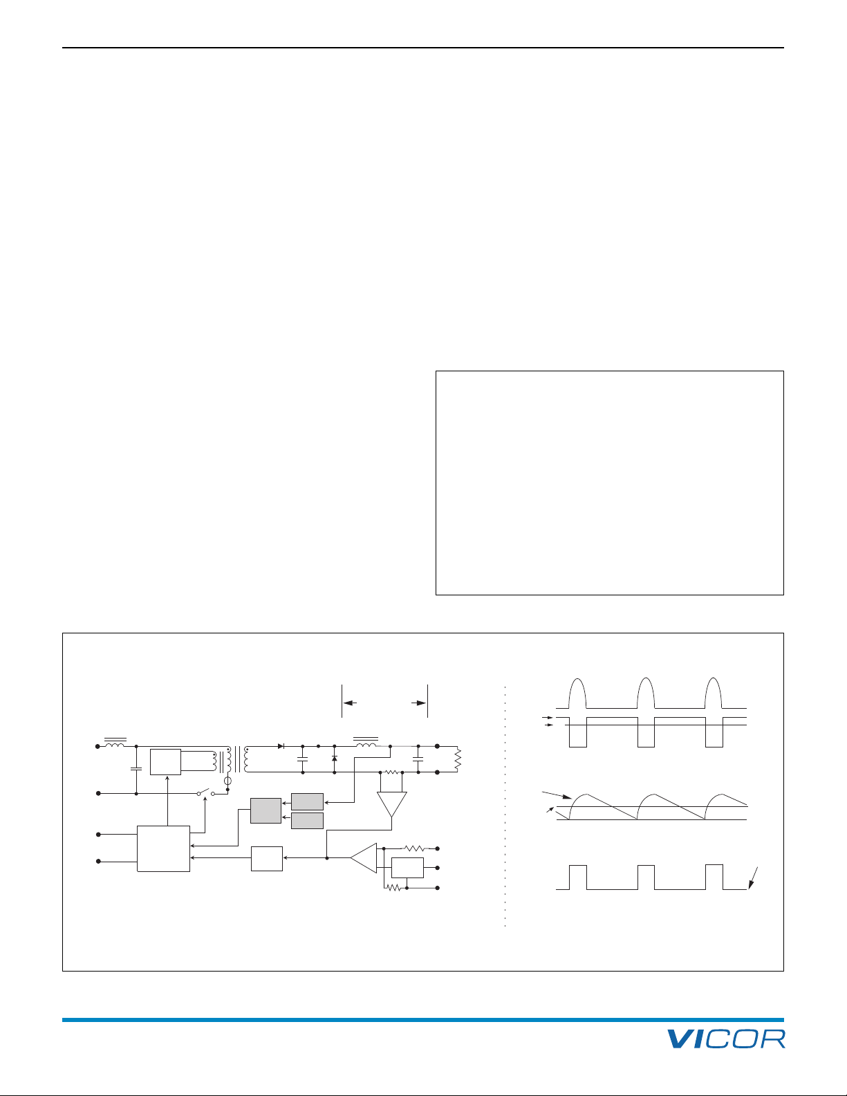
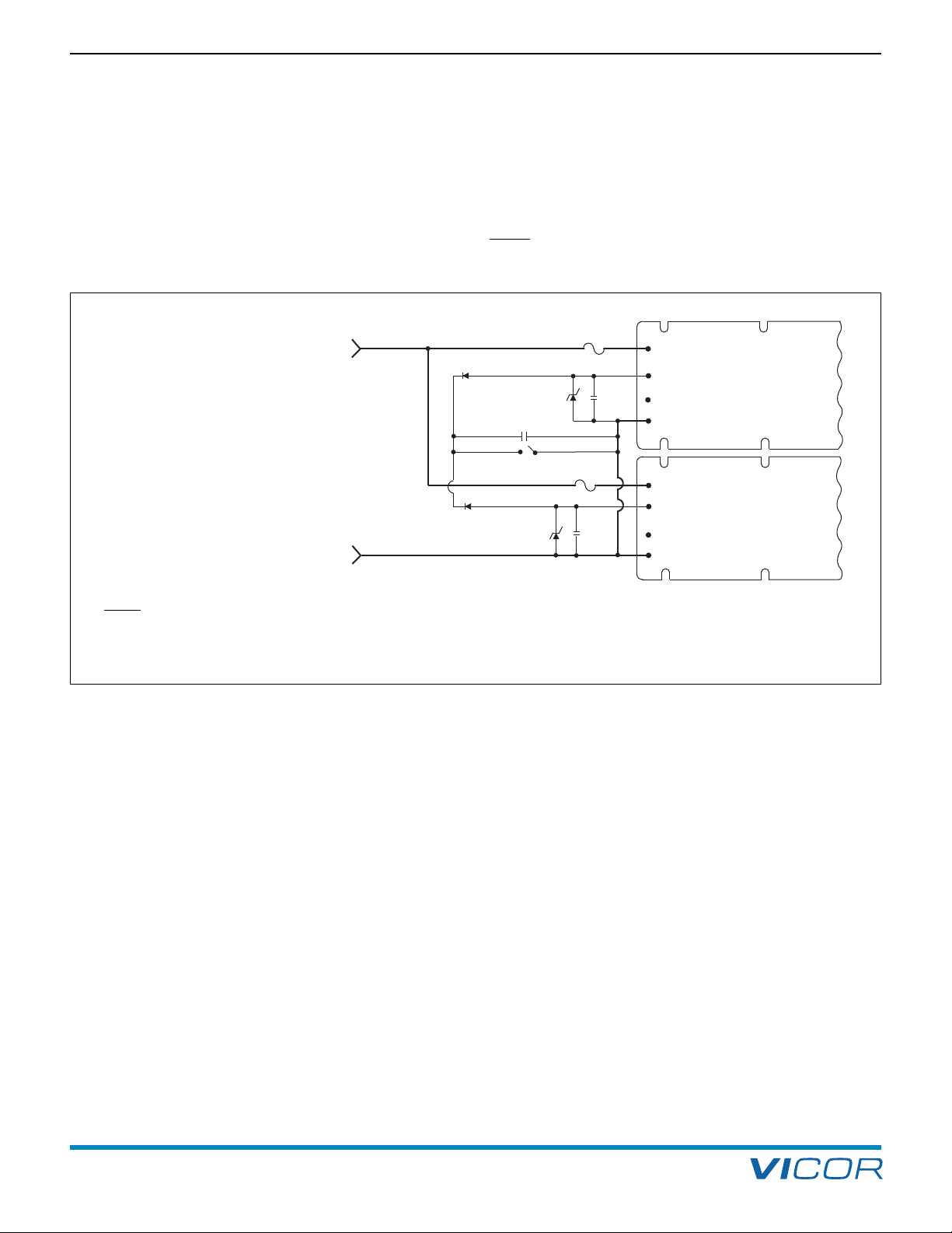
1. Zero-Current-Switching
or VI-200 and VI-J00 Family DC-DC Converters and Configurable Power Supplies
F
Design Guide & Applications Manual
OVERVIEW
Vicor offers RoHS compliant modules. These modules have
a “VE” prefix. The information presented herein applies to
both versions, and “VI” will be the default designation.
he heart of Vicor’s VI-/ MI-200 and VI-/ MI-J00 module
T
technology, zero-current-switching, allows Vicor
converters to operate at frequencies in excess of 1 MHz,
with high efficiency and power density. Depending on
input voltage and load, the converters operate at
frequencies ranging from the low hundreds of kilohertz
(light load, high line) to approximately one megahertz (full
load, low line). Another aspect of the Vicor topology is
that two or more power trains driven at the same
frequency will inherently load-share if their outputs are
tied together. Load sharing is dynamic and is within 5%.
The VI-200 and MI-200 product line offer both Driver and
Booster modules:
• Drivers and Boosters must have identical power trains.
• Drivers close the voltage loop internally, Boosters do not.
• Boosters may be slaved to a Driver, allowing
configurations of multi-kilowatt arrays, which
exhibit dynamic current sharing between modules.
• Only a single control connection is needed between
modules with all module’s power inputs and outputs,
connected together — no trimming, adjustments, or
external components are required to achieve load sharing.
LOSSLESS ENERGY TRANSFER
Referring to Figure and Table 1–1 below, turn-on of the
MOSFET switch transfers a quantized energy packet from
the input source to an LC “tank” circuit, composed of
inherent transformer leakage inductance of T1 and a
capacitive element, C, in the secondary. Simultaneously,
an approximately half-sinusoidal current flows through the
switch, resulting in switch turn-on at zero current and
turn-off when current returns to zero. Resonance, or
bidirectional energy flow, cannot occur because D1 will
only permit unidirectional energy transfer. A low-pass filter
(Lo, Co) following the capacitor produces a low ripple DC
output. The result is a virtually lossless energy transfer
from input to output with greatly reduced levels of
conducted and radiated noise.
Ip: Primary current
Vp: Primary voltage
Vs: Secondary voltage
OVP: Overvoltage protection (output)
OTS: Over temperature shutdown
OC1, OC2: Opto-coupler
E/A: Error amplifier
REF: Bandgap reference
C/L: Current limit amplifier
Table 1–1
Apps. Eng. 800 927.9474 800 735.6200
Figure 1–1 — VI-/MI-200 and VI-/MI-J00 series zero-current-switching block diagram
VI-200 and VI-J00 Family Design Guide Rev 3.5 vicorpower.com
Page 2 of 98
Page 4
Design Guide & Applications Manual
GATE
IN
G
ATE
OUT
+IN
–
OUT
–S
T
+S
+OUT
GATE
IN
GATE
OUT
+IN
–OUT
–S
T
+S
–IN
–IN
+OUT
or VI-200 and VI-J00 Family DC-DC Converters and Configurable Power Supplies
F
Figure 2–1 — VI-/MI-200, VI- / MI-J00
–IN, + IN. DC voltage inputs. See Tables 2–1 and 2–2 for
nominal input voltages and ranges for the VI-/MI-200 and
VI-/MI-J00 Family converter modules (data sheets contain
Low Line, 75% Max. Power and Transient ratings).
VI-200, VI-J00 Input Voltage Ranges
Designator Low Nominal High
0 10 V 12 V 20 V
V 10 V12/24 V 36 V
1 21 V 24 V 32 V
W 18 V 24 V 36 V
2 21 V 36 V 56 V
3 42 V 48 V 60 V
N 36 V 48 V 76 V
4 55 V 72 V 100 V
T 66 V 110 V 160 V
5 100 V 150 V 200 V
6 200 V 300 V 400 V
7 100 V 150/300 V 375 V
Table 2–1 — VI-200, VI-J00 input voltage ranges
MI-200, MI-J00 Input Voltage Ranges
Designator Low Nominal High
2 18 V 28 V 50 V
5 100 V 155 V 210 V
6 125 V 270 V 400 V
7 100 V 165 V 310 V
Table 2–2 — MI-200, MI-J00 input voltage ranges
2. DC-DC Converter Pinouts
GATE IN. The GATE IN pin on a Driver module may be
used as a logic Enable / Disable input. When GATE IN is
pulled low (<0.65 V @ 6 mA, referenced to –Vin), the
odule is turned off; when GATE IN is floating (open
m
collector), the module is turned on. The open circuit
oltage of the GATE IN pin is less than 10 V.
v
–OUT, +OUT. DC output pins. See the Table 2–3 and 2–4
below for output voltages and power levels of VI-/MI-200
and VI-/MI-J00 Family converter modules.
VI-200, VI-J00 Standard Output Voltages
Designator Output Designator Output
Z2V 215 V
Y 3.3 VN18.5 V
05V 324 V
X 5.2 VL28 V
W 5.5 VJ36 V
V 5.8 VK40 V
T 6.5 V448 V
R 7.5 VH52 V
M 10 VF72 V
1 12 VD85 V
P 13.8 VB95 V
Table 2–3 — VI-200, VI-J00 output voltage designators
Output
Voltage
<5 Vdc 10 – 40 A 5 – 20 A 10 – 30 A 5 – 10 A
≥5 Vdc 50 – 200 W 25 – 100 W 50 – 100 W 10 – 50 W
Table 2–4 — Output voltage vs. power level
Special output voltages from 1 – 95 V; consult factory.
T (TRIM). Provides fixed or variable adjustment of the
module output.
Trimming Down. Allows output voltage of the module to
be trimmed down, with a decrease in efficiency. Ripple as
a percent of output voltage goes up and input range
widens since input voltage dropout (loss of regulation)
moves down.
Trimming Up. Reverses the above effects.
Power Level Power Level
VI-200 VI-J00 MI-200 MI-J00
–S, +S (–SENSE, +SENSE). Provides for locating the point
of optimal voltage regulation external to the converter.
GATE OUT. The pulsed signal at the GATE OUT pin of a
regulating Driver module is used to synchronously drive
the GATE IN pin of a companion Booster module to effect
power sharing between the Driver and the Booster. Daisychaining additional Boosters (connecting GATE OUT of
one unit to GATE IN of a succeeding unit) leads to a
virtually unlimited power expansion capability.
Output OVP in VI-/MI-200 will trip if remote sense
compensates output voltage measured at output pins
above 110% of nominal. Discrete wire used for sense
must be tightly twisted pair. Do not exceed 0.25 V drop in
negative return; if the voltage drop exceeds 0.25 V in the
negative return path, the current limit setpoint will increase.
Connect +SENSE to +OUT and –SENSE to –OUT at the
module if remote sensing is not desired.
VI-200 and VI-J00 Family Design Guide Rev 3.5 vicorpower.com
Page 3 of 98
Apps. Eng. 800 927.9474 800 735.6200
(Figure 7–4)
Page 5

3. Module Do’s and Dont’s
or VI-200 and VI-J00 Family DC-DC Converters and Configurable Power Supplies
F
Design Guide & Applications Manual
ELECTRICAL CONSIDERATIONS
GATE IN AND GATE OUT PINS
Logic Disable. When power is applied to the input pins,
the GATE IN pin of a Driver can be pulled low with respect
to the –IN thus turning off the output while power is still
applied to the input. (Figure 7–1)
CAUTION: With offline applications –IN is not
earth ground.
In Logic Disable mode, the GATE IN pin should be driven
from either an “open collector” or electromechanical
switch that can sink 6 mA when on (GATE IN voltage less
than 0.65 V). If driven from an electromechanical switch
or relay, a 1 µF capacitor should be connected from GATE IN
to –IN to eliminate the effects of switch “bounce”. The 1 µF
capacitor may be required in all applications to provide a
“soft start” if the unit is disabled and enabled quickly. Do
not exceed a repetitive on / off rate of 1 Hz to the GATE
IN or input voltage pins.
High Power Arrays. The pulsed signal at the GATE OUT
pin of a regulating Driver module is used to synchronously
drive the GATE IN pin of a companion Booster module to
effect power sharing between the Driver and the Booster.
(Figure 7–5) Daisy-chaining additional Boosters (i.e.,
connecting GATE OUT to GATE IN of a succeeding unit)
leads to a virtually unlimited power expansion capability.
VI-/MI-200 series modules of the same family and power
level can be paralleled (i.e., Driver, VI-260-CU with
Booster, VI-B60-CU).
In general:
• Don’t drive the GATE IN pin from an “analog”
voltage source.
• Don’t leave GATE IN pins of Booster modules
unterminated.
• Don’t overload GATE OUT; limit load to a single Vicor
module GATE IN connection, or 1 kΩ, minimum, in
parallel with 100 pF, maximum.
• Don’t skimp on traces that interconnect module –IN
pins in high power arrays. GATE IN and GATE OUT
are referenced to –IN; heavy, properly laid out traces will
minimize parasitic impedances that could interfere with
proper operation.
• Do use a decoupling capacitor across each module’s
input (see Input Source Impedance that follows).
• Do use an EMI suppression capacitor from +/– input and
output pins to the baseplate.
• Do use a fuse on each module’s + input to prevent fire
in the event of module failure. See safety agency
conditions of acceptability for the latest information on
fusing. Please see the Vicor website
for Safety Approvals.
Input Source Impedance. The converter should be
connected to an input source that exhibits low AC
impedance. A small electrolytic capacitor should be
ounted close to the module’s input pins. (C3, Figure 3–1)
m
This will restore low AC impedance, while avoiding the
otential resonance associated with “high-Q” film
p
capacitors. The minimum value of the capacitor, in
microfarads, should be C (µF) = 400 ÷ Vin minimum.
Example: Vin, minimum, for a VI-260-CV is 200 V. The
minimum capacitance would be 400 ÷ 200 = 2 µF. For
applications involving long input lines or high inductance,
additional capacitance will be required.
The impedance of the source feeding the input of the
module directly affects both the stability and transient
response of the module. In general, the source impedance
should be lower than the input impedance of the module
by a factor of ten, from DC to 50 kHz.
To calculate the required source impedance, use the
following formula:
L
n
L
Z = 0.1(V
)2/ Pi
where: Z is required input impedance
VLL is the low line input voltage
Pin is the input power of the module
Filters, which precede the module, should be well damped
to prevent ringing when the input voltage is applied or
the load on the output of the module is abruptly changed.
Input Transients. Don’t exceed the transient input
voltage rating of the converter. Input Attenuator Modules
or surge suppressors in combination with appropriate
filtering, should be used in offline applications or in
applications where source transients may be induced by
load changes, blown fuses, etc. For applications where the
input voltage may go below low line it is recommended
that an undervoltage lockout circuit be used to pull GATE
IN low to disable the converter module. The undervoltage
lockout circuit should induce a delay of at least one
second before restarting the converter module. Longer
delays will be required if external capacitance is added at
the output to insure the internal soft-start is re-initialized.
NOTE: Do not allow the rate of change of the input
voltage to exceed 10 V/µs for any input voltage deviation.
The level of transient suppression required will depend on
the severity of the transients. A Zener diode, TRANSZORB™
or MOV will provide suppression of transients under 100 µs
and act as a voltage clipper for DC input transients. It may
be necessary to incorporate an LC filter for larger energy
transients. This LC filter will integrate the transient energy
while the Zener clips the peak voltages. The Q of this filter
should be kept low to avoid potential resonance problems.
See Section 14, Input Attenuator Module (IAM / MI-IAM)
for additional information on transient suppression.
VI-200 and VI-J00 Family Design Guide Rev 3.5 vicorpower.com
Page 4 of 98
Apps. Eng. 800 927.9474 800 735.6200
Page 6
Design Guide & Applications Manual
+OUT
+IN
–IN
–OUT
Zero Current
Switching
Converter
C1a
C1b
C2a
C2b
C3
or VI-200 and VI-J00 Family DC-DC Converters and Configurable Power Supplies
F
3. Module Do’s and Dont’s
Output OVP. The VI-/MI-200, with the exception of
I-/ MI-J00s, has an internal overvoltage protection circuit
V
that monitors the voltage across the output power pins. It
is designed to latch the converter off at 115 – 135% of
rated output voltage. It is not a crowbar circuit, and if a
module is trimmed above 110% of rated output voltage,
OVP may be activated. Do not backdrive the output of
the converter module to test the OVP circuit.
CAUTION:
When trimming up VI-/MI-J00 modules,
additional care should be taken as an improper
component selection could result in module failure.
Improper connection of the sense leads on VI-/MI-J00
modules can also result in an excessive overvoltage
condition and module failure.
Input Reverse Voltage Protection. The module may be
protected against reverse input voltages by the addition of
a diode in series with the positive input, or a reverse
shunt diode with a fuse in series with the positive input.
See Section 14, the Input Attenuator Module (IAM/MI-IAM)
provides input reverse voltage protection when used with
a current limiting device (fuse).
THERMAL / MECHANICAL CONSIDERATIONS
Baseplate. Operating temperature of the baseplate, as
measured at the center mounting slot on the –IN, –OUT
side, can not exceed rated maximum. ThermMate or
thermal compound should be used when mounting the
module baseplate to a chassis or heat sink. All six
mounting holes should be used. Number six (#6) machine
screws should be torqued to 5-7 in-lbs, and use of Belville
washers is recommended.
THERMAL AND VOLTAGE HAZARDS
Vicor component power products are intended to be used
ithin protective enclosures. Vicor DC-DC converters
w
work effectively at baseplate temperatures, which could
be harmful if contacted directly. Voltages and high
currents (energy hazard) present at the pins and circuitry
connected to them may pose a safety hazard if contacted
or if stray current paths develop. Systems with removable
circuit cards or covers which may expose the converter(s)
or circuitry connected to the converters, should have proper
guarding to avoid hazardous conditions.
EMC CONSIDERATIONS
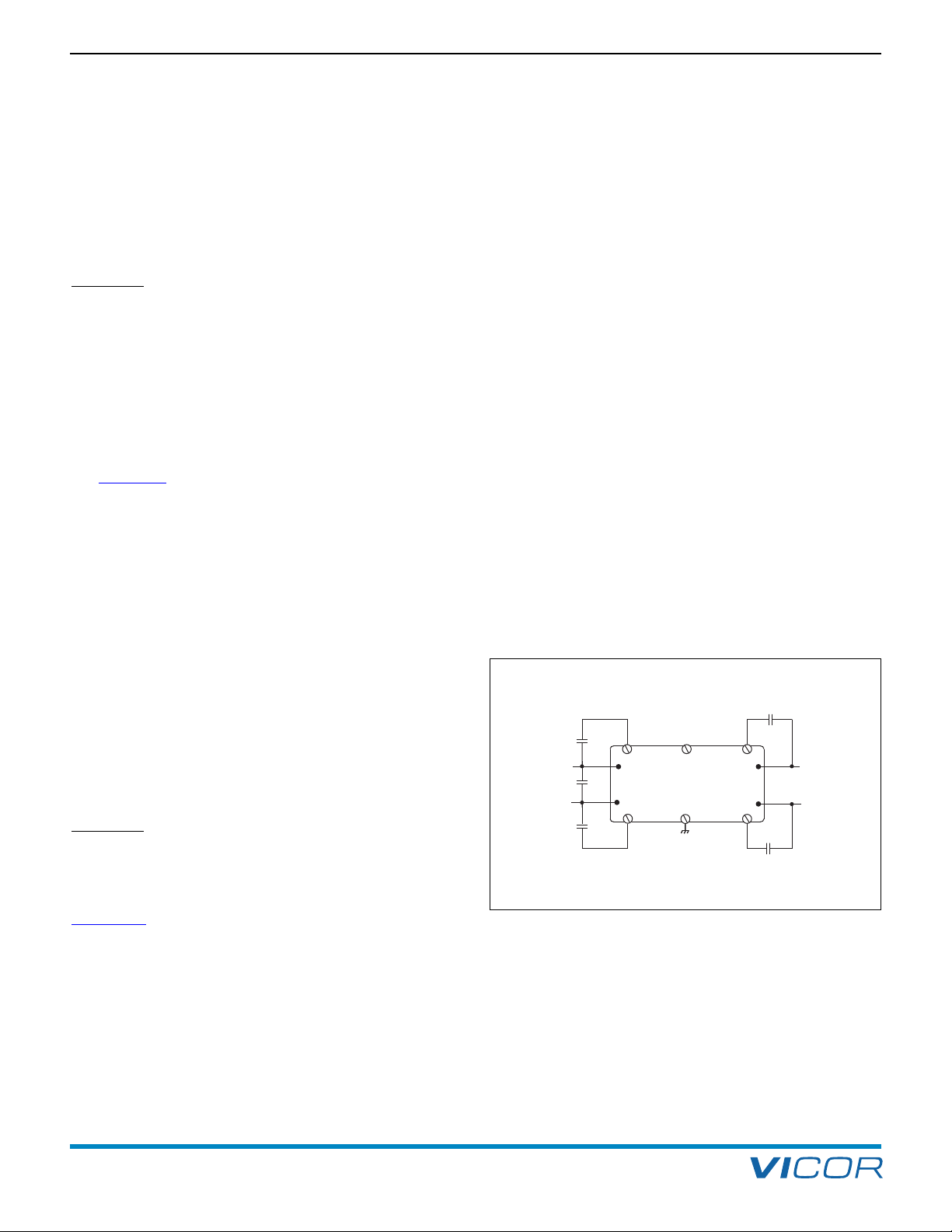
All applications utilizing DC-DC converters must be properly
bypassed, even if no EMC standards need to be met. Bypass
IN and OUT pins to each module baseplate as shown in
Figure 3–1. Lead length should be as short as possible.
Recommended values vary depending on the front end, if
any, that is used with the modules, and are indicated on the
appropriate data sheet. In most applications, C1a – C1b is a
4,700 pF Y-capacitor (Vicor Part # 01000) carrying the
appropriate safety agency approval; C2a – C2b is a 4,700 pF
Y-capacitor (Vicor Part # 01000) or a 0.01 µF ceramic
capacitor rated at 500 V. In PCB mount applications, each of
these components is typically small enough to fit under the
module baseplate flange.
The module pins are intended for PCB mounting either by
wave soldering to a PCB or by insertion into one of the
recommended PCB socket solutions.
CAUTION: Use of discrete wires soldered directly
to the pins may cause intermittent or permanent
damage to the module; therefore, it is not
recommended as a reliable interconnection scheme
for production as a final released product. See
Section 21 for packaging options designed for
discrete wire connections (BusMod, MegaMod).
Figure 3–1 — IN and OUT pins bypassed to the module baseplate
and input cap for low AC impedance
In addition, modules that have been soldered into printed
circuit boards and have subsequently been removed
should not be reused.
VI-200 and VI-J00 Family Design Guide Rev 3.5 vicorpower.com
Page 5 of 98
Apps. Eng. 800 927.9474 800 735.6200
Page 7
3. Module Do’s and Dont’s
SAFETY CONSIDERATIONS
or VI-200 and VI-J00 Family DC-DC Converters and Configurable Power Supplies
F
Design Guide & Applications Manual
Shock Hazard. Agency compliance requires that the
baseplate be grounded.
Fusing. Internal fusing is not provided in Vicor DC-DC
onverters. To meet safety agency conditions, a fuse is
c
required. This fuse should be placed in the positive input
lead, not the negative input lead, as opening of the
negative input lead will cause the GATE IN and GATE OUT
to rise to the potential of the +IN lead, causing possible
damage to other modules or circuits that share common
GATE IN or GATE OUT connections.
Acceptable Fuse Types and Current Rating for the VI-200 and VI-J00 Family of Converters
Package Size Required Fuse Package Size Required Fuse
VI-27x-xx PC-Tron 2.5 A VI-J7x-xx PC-Tron 2.5 A
VI-26x-xx PC-Tron 3 A VI-J6x-xx PC-Tron 3 A
VI-25x-xx PC-Tron 5 A VI-J5x-xx PC-Tron 5 A
VI-2Tx-xx PC-Tron 5A VI-JTx-xx PC-Tron 5A
VI-24x-xx 6 A / 125 V VI-J4x-xx PC-Tron 5A
Safety agency conditions of acceptability require module
input fusing. The VI-x7x, VI-x6x and VI-x5x require the use
of a Buss PC-Tron fuse, or other DC-rated fuse. See below
for suggested fuse ratings.
The safety approvals section of the Vicor website should
always be checked for the latest fusing and conditions of
acceptability information for all DC-DC converters
including the MegaMod family.
VI-2Nx-xx 8A / 125 V VI-JNx-xx PC-Tron 5A
VI-23x-xx 8 A /125 V VI-J3x-xx PC-Tron 5A
VI-22x-xx 8 A / 60 V VI-J2x-xx PC-Tron 5A
VI-2Wx-xx 12 A / 50 V VI-JWx-xx 8 A / 60 V
VI-21x-xx 12 A / 32 V VI-J1x-xx 8 A / 60 V
VI-2Vx-xx 12 A / 32 V VI-J0x-xx 8 A / 60 V
VI-20x-xx 12 A / 32 V
VI-200 and VI-J00 Family Design Guide Rev 3.5 vicorpower.com
Page 6 of 98
Apps. Eng. 800 927.9474 800 735.6200
Page 8
Design Guide & Applications Manual
2 V
V
out
I
c
I
fb
I
max
I
out
I
short circuit
V
out
I
short circuit
I
c
I
max
I
out
or VI-200 and VI-J00 Family DC-DC Converters and Configurable Power Supplies
F
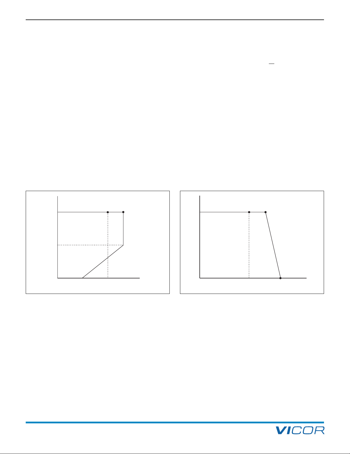
4. Overcurrent Protection
FOLDBACK CURRENT LIMITING
The VI-/MI-200 modules with output voltages of 5 V or
3.3 V incorporate foldback current limiting. (Figure 4–1) In
his mode, the output voltage remains constant up to the
t
current knee, (Ic), which is 5 – 25% greater than full-rated
urrent, (Imax). Beyond Ic, the output voltage falls along
c
the vertical line Ic– Ifb until approximately 2 V. At ≤2 V, the
voltage and current folds back to short circuit current
point (20 – 80% of Imax). Typically, modules will
automatically recover when overcurrent is removed.
When bench testing modules with foldback current limiting,
use a constant resistance load as opposed to a constant
current load. Some constant current loads have the ability
to pull full current at near zero volts. This may cause a
latchup condition. Also when performing a short circuit
test it is recommended to use a mercury wetted relay to
induce the output short as other methods may induce
switch bounce that could potentially damage the converter.
STRAIGHT LINE CURRENT LIMITING
The VI-/MI-200 modules with output voltages greater
than 5 V, 2 V (VI-/MI-200 only) and all
odules incorporate a straight-line type current limit.
m
VI-/MI-J00
(Figure 4–2) As output current is increased beyond Imax,
he output voltage remains constant and within its
t
specified limits up to a point, Ic, which is 5 – 25% greater
than rated current, (Imax). Beyond Ic, the output voltage
falls along the vertical line to Isc. Typically, modules will
automatically recover after overcurrent is removed.
Figure 4–1 — Foldback current limiting
Apps. Eng. 800 927.9474 800 735.6200
VI-200 and VI-J00 Family Design Guide Rev 3.5 vicorpower.com
Page 7 of 98
Figure 4–2 — Straight-line current limiting
Page 9
5. Output Voltage Trimming
+OUT
+SENSE
–OUT
R
3
–
+
C1
Load
[
a]
F
or Vout < 3.3 V, R5 = 3.88 kΩ and internal reference = 0.97 V.
E
rror Amp
R
1 47 Ω Typ.
R4 27 Ω Typ.
R2
R
5 10 kΩ
[
a]
TRIM
R6
–SENSE
R8
R
7
2.5 V
[a]
R6
TRIM
–SENSE
–OUT
R7 10 kΩ POT
R5 10 kΩ
[a]
(internal)
V1
R8
I
R6
2.5 V
[a]
reference
(internal)
[a]
For Vout < 3.3 V, R5 = 3.88 kΩ and internal reference = 0.97 V.
+OUT
+SENSE
–SENSE
OVERVIEW
or VI-200 and VI-J00 Family DC-DC Converters and Configurable Power Supplies
F
Design Guide & Applications Manual
Specifications such as efficiency, ripple and input voltage
range are a function of output voltage settings. As the
output voltage is trimmed down, efficiency goes down;
ripple as a percent of Vout goes up and the input voltage
range widens since input voltage dropout (loss of regulation)
moves down. As the units are trimmed up, the reverse of
the above effects occurs.
All converters have a fixed current limit. The overvoltage
protection setpoint is also fixed; trimming the output
voltage does not alter its setting. As the output voltage is
trimmed down, the current limit setpoint remains constant.
Therefore, in terms of output power, if the unit is trimmed
down, available output power drops accordingly.
The output voltage of most Vicor converters can be
trimmed +10%, –50%. Certain modules have restricted
trim ranges. Consult the latest datasheet for details.
Do not attempt to trim the module output voltage more
than +10%, as overvoltage shut down may occur. Do not
exceed maximum rated output power when the module is
trimmed up.
CAUTION: When trimming up VI- / MI-J00 converter
modules, additional care should be taken as an
improper component selection could result in module
failure. Improper connection of the sense leads on
VI-/ MI-J00 converter modules can also result in an
excessive overvoltage condition and module failure.
Example 1. For trimming –10% to +10% with a standard
off-the-shelf 10 kΩ potentiometer (R7), values for resistors
R6 and R8 need to be calculated.
esistor R6 limits the trim down range. For a given
R
percentage, its value is independent of output voltage.
Refer to
Figure 5–1 — External resistive network for variable trimming
Table 5–1, for limiting resistor values.
TRIMMING DOWN –10%
A 10% drop of the 2.5 V reference at the TRIM pin is
needed to effect a 10% drop in the output voltage.
(Figure 5–2)
The following procedures describe methods for output
voltage adjustment (–10 to +10% of nominal) of the
VI-/MI-200, VI-/MI-J00, ComPAC/MI-ComPAC, FlatPAC
and MegaMod / MI-MegaMod Families.
Modules with nominal 3.3 V outputs and above have
the 2.5 V precision reference and 10 k internal resistor.
For trim resistor calculations on modules with 2.0 V
outputs use 0.97 V in place of the 2.5 V reference
and substitute 3.88 kΩ for the internal 10 kΩ resistor.
Figure 5–2 — Circuit diagram “Trim Down”
Resistors are 0.25 W. When trimming down any module,
always maintain a minimum preload of at least 1% of
rated output power and in some cases up to 10% may be
required. For more specific information on trimming down
Therefore:
a specific module, please consult Vicor’s Applications
Engineering Department at (800) 927-9474.
RESISTIVE ADJUSTMENT PROCEDURE
Since IR5 = IR6 = 25 µA:
To achieve a variable trim range, an external resistor
network must be added. (Figure 5–1)
VI-200 and VI-J00 Family Design Guide Rev 3.5 vicorpower.com
Page 8 of 98
Apps. Eng. 800 927.9474 800 735.6200
This value will limit the trim down range to –10% of
nominal output voltage.
V1 = 2.5 V – 10% = 2.25 V
(2.5 V – 2.25 V)
IR5 =
R6 =
10 kΩ
2.25 V
25 µA
= 25 µA
= 90 kΩ
Page 10
Design Guide & Applications Manual
I
V2
R6 90 kΩ
TRIM
+ SENSE
–
SENSE
– OUT
R
5 10 kΩ
[a]
(internal)
V
1
R
8
R
8
R
7 10 kΩ POT
500 µA
25 µA
2.5 V
[a]
r
eference
(internal)
+ OUT
[a]
For Vout < 3.3 V, R5 = 3.88 kΩ and inter nal reference = 0.97 V.
TRIM
+ OUT
+ SENSE
– SENSE
– OUT
Rd
Ru
Trim Resistor for UP
Programming
Trim Resistor for DOWN
Programming
or
2.5 V
[a]
reference
(internal)
R5 10 kΩ
[a]
(internal)
[a]
For Vout < 3.3 V, R5 = 3.88 kΩ and inter nal reference = 0.97 V.
or VI-200 and VI-J00 Family DC-DC Converters and Configurable Power Supplies
F
5. Output Voltage Trimming
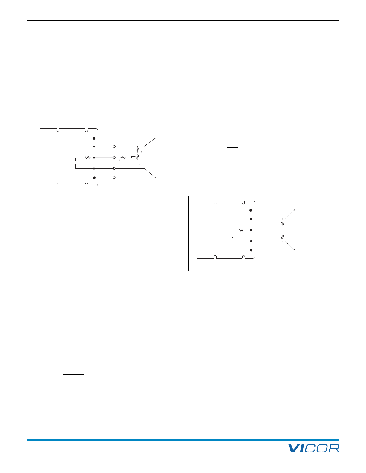
TRIMMING UP +10%
To trim 10% above the nominal output voltage, the
following calculations are needed to determine the value
of R8. This calculation is dependent on the output voltage
of the module. A 12 V output will be used as an example.
(Figure 5–3)
It is necessary for the voltage at the TRIM pin to be 10%
greater than the 2.5 V reference. This offset will cause the
error amplifier to adjust the output voltage up 10% to 13.2 V.
Figure 5–3 — Circuit diagram “Trim Up”
FIXED TRIM
Converters can be trimmed up or down with the addition
of one external resistor, either Ru for programming up or
Rd for programming down. (Figure 5–4)
xample 2. Fixed Trim Up (12 V to 12.6 V).
E
To determine Ru, the following calculation must be made:
2.5 V + 5% = 2.625 V
5
= VT
RIM
R
V
– Vr
ef
VR5= 2.625 – 2.5 = 0.125 V
Knowing this voltage, the current through R5 can be found:
IR5 =
VR5
R5 10 kΩ
=
0.125
= 12.5 µA
VRu = 12.6 V – 2.625 V = 9.975 V
9.975
Ru =
12.5 µA
= 798 kΩ
V1 = 2.5 V + 10% = 2.75 V
(2.75 V – 2.5 V)
IR5 =
10 kΩ
= 25 µA
Since IR5 = IR6 ,
the voltage drop across R6 = (90 kΩ) (25 µA) = 2.25 V.
Figure 5–4 — Fixed trimming
Therefore, V2 = 2.75 V + 2.25 V = 5 V. The current
through R7 (10 kΩ pot) is:
IR7 =
V2
R7 10 k
5
=
= 500 µA
Using Kirchoff’s current law:
R8 = IR7 + IR6 = 525 µA
I
Thus, knowing the current and voltage, R8 can be
determined:
VR8 = (Vout + 10%) – V2 = 13.2 V – 5 V = 8.2 V
R8 =
(8.2 V)
525 µA
= 15.6 kΩ
Connect Ru from the TRIM pin to the +SENSE. Be sure to
connect the resistor to the +SENSE, not the +OUT, or
drops in the positive output lead as a function of load will
cause apparent load regulation problems.
Example 3. –25% Fixed Trim Down (24 V to 18 V).
The trim down methodology is identical to that used in
Example 2, except that it is utilized to trim the output of a
24 V module down 25% to 18 V. The voltage on the
TRIM pin must be reduced 25% from its nominal setting
of 2.5 V. This is accomplished by adding a resistor from
the TRIM pin to –SENSE.
2.5 V – 25% = 1.875 V
This resistor configuration allows a 12 V output module
to be trimmed up to 13.2 V and down to 10.8 V. Follow
this procedure to determine resistor values for other
output voltages.
VI-200 and VI-J00 Family Design Guide Rev 3.5 vicorpower.com
Page 9 of 98
Apps. Eng. 800 927.9474 800 735.6200
VR5 = Vbandgap – VTRIM
= 2.5 V – 1.875 V = 0.625 V
Page 11
5. Output Voltage Trimming
or VI-200 and VI-J00 Family DC-DC Converters and Configurable Power Supplies
F
Design Guide & Applications Manual
Knowing this voltage, the current through R5 can be found:
IR5 =
VR
R5 10 kΩ
=
0.625
= 62.5 µA
5
The voltage across the resistor, Rd, and the current
lowing through it are known:
f
Rd =
(2.5 V – 0.625 V)
= 30 kΩ
62.5 µA
Connect Rd (Figure 5–4) from the TRIM pin to the –SENSE
of the module. Be sure to connect the resistor to the
–SENSE, not the –OUT, or drops in the negative output
lead as a function of load will cause apparent load
regulation problems.
Values for Trim Down by Percentage
Percent Resistance
–5 % 190 kΩ
–10 % 90 kΩ
–15 % 56.7 kΩ
–20 % 40 kΩ
–25 % 30 kΩ
–30 % 23.3 kΩ
–35 % 18.6 kΩ
–40 % 15 kΩ
–45 % 12.2 kΩ
–50 % 10 kΩ
Table 5–1 — Values for trim down by percentage (Refer to product
data sheet for allowable trim ranges at
vicorpower.com)
Fixed Trim Down
Vnom V (Desired) Trim Resistor
5V 4.5 V 90.9 kΩ
3.3 V 19.6 kΩ
2.5 V 10.0 kΩ
15 V 13.8 V 115 kΩ
24 V 20 V 49.9 kΩ
48 V 40 V 49.9 kΩ
36 V 30.1 kΩ
Table 5–2a — Values for fixed trim down by voltage
[a]
DYNAMIC ADJUSTMENT PROCEDURE
Output voltage can also be dynamically programmed by
driving the TRIM pin from a voltage or current source;
programmable power supplies and power amplifier
applications can be addressed in this way. For dynamic
programming, drive the TRIM pin from a source referenced
to the negative sense lead, and keep the drive voltage in
the range of 1.25 – 2.75 V. Applying 1.25 – 2.5 V on the
TRIM pin corresponds to 50 – 100% of nominal output
voltage. For example, an application requires a +10, 0%
(nominal), and a –15% output voltage adjustment for a 48 V
output converter. Referring to the table below, the voltage
that should be applied to the trim pin would be as follows:
VT
RIM
VO
UT
Change from nominal
2.125 40.8 –15%
2.5 48 0
2.75 52.8 +10%
The actual voltage range is further restricted by the
allowable trim range of the converter. Voltages in excess
of 2.75 V (+10% over nominal) may cause overvoltage
protection to be activated. For applications where the
module will be programmed on a continuous basis the
slew rate should be limited to 30 Hz sinusoidal.
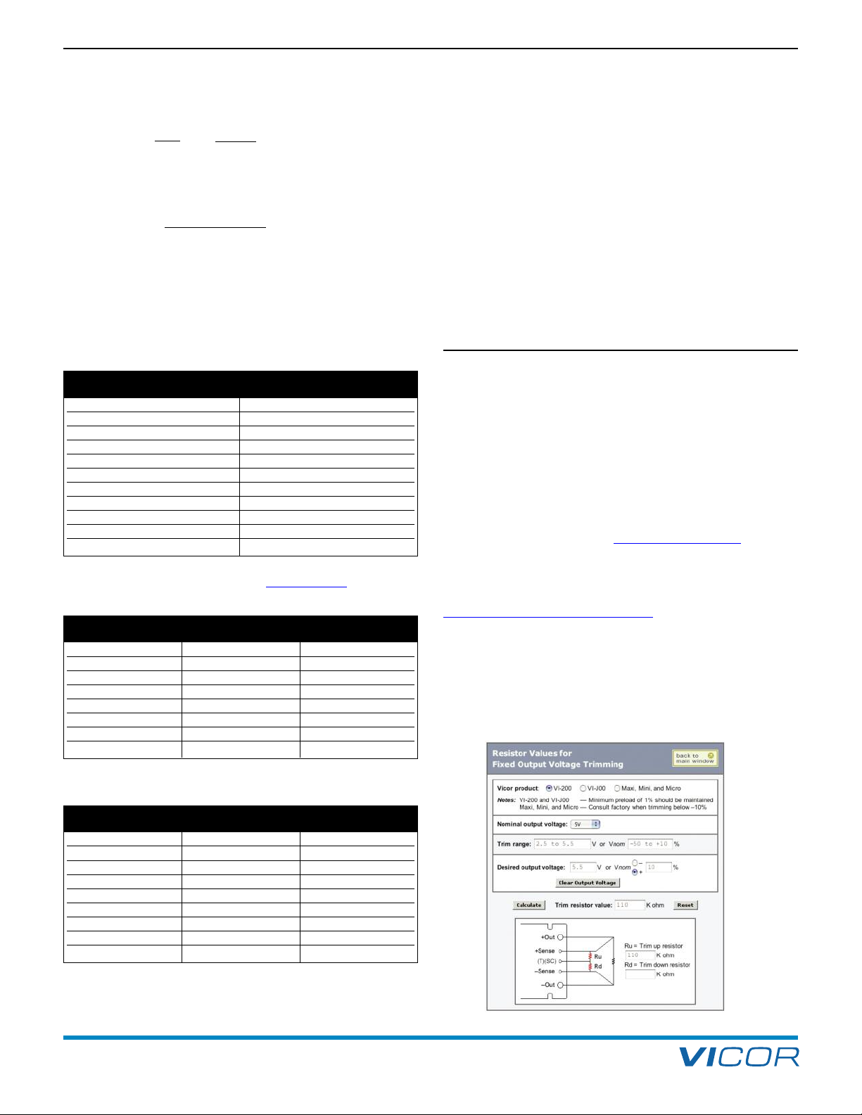
TRIMMING ON THE WEB (VICORPOWER.COM)
Trim values are calculated automatically. Design
Calculators are available on Vicor’s website in the
PowerBenchTMsection at
www.vicorpower.com/powerbench.
Resistor values can be easily determined for fixed trim up,
fixed trim down and for variable trimming applications.
In addition to trimming information, the website also
includes design tips, applications circuits, EMC
suggestions, thermal design guidelines and PDF data
sheets for all available Vicor products.
Fixed Trim Up
Vnom V (Desired) Trim Resistor
5V 5.2 V 261 kΩ
5.5 V 110 kΩ
12 V 12.5 V 953 kΩ
13.2 V 422 kΩ
15 V 15.5 V 1.62 MΩ
16.5 V 562 kΩ
24 V 25 V 2.24 MΩ
48 V 50 V 4.74 MΩ
Table 5–2b — Values for fixed trim up by voltage
[a]
Values listed in the tables are the closest standard 1% resistor values.
VI-200 and VI-J00 Family Design Guide Rev 3.5 vicorpower.com
Page 10 of 98
Apps. Eng. 800 927.9474 800 735.6200
[a]
Page 12
Design Guide & Applications Manual
+IN
–IN
GATE
OUT
GATE
IN
+IN
–IN
GATE
OUT
GATE
IN
Vicor
DC-DC Converter
F1
C1
Z1
C3
SW1
F2
DISABLE
D2
Z2 C2
D1
Vicor
DC-DC Converter
or VI-200 and VI-J00 Family DC-DC Converters and Configurable Power Supplies
F
OVERVIEW
6. Multiple GATE IN Connections
A number of GATE IN pins may be connected for remote
shut down and logic disable. (Figure 6-1) Diodes D1 and
D2 provide isolation and prevent multiple failures if the
GATE IN of a module becomes shorted to the +IN. The
Zener diodes Z1, Z2 and capacitors C1, C2 attenuate
transient voltage spikes caused by differential inductance
in the negative lead. Capacitors C1 and C2 will also
C1, C2, C3 = 1 µF
Z1, Z2 = 15 V (1N5245B)
D1, D2 = Small signal diode (1N4148)
[a]
For bus voltages greater than 75 V,
a 1N4006 diode should be used.
[a]
lengthen turn-on time. SW1 is a mechanical or solid state
switch that is used to disable both Driver modules. C3 is
used to minimize the effects of “switch bounce” associated
with mechanical devices.
NOTE: GATE IN voltage needs to be <0.65 V
referenced to –IN to ensure modules are disabled.
NOTE:
The –IN to –IN input lead should be kept as short as possible to minimize differential inductance.
Heavy lines indicate power connections. Use suitably sized conductors.
Opto-couplers or relays should be used to isolate GATE IN connections, if the converters are on
separate boards or the negative input lead’s impedance is high.
Figure 6–1 — Protection for multiple GATE IN connections
VI-200 and VI-J00 Family Design Guide Rev 3.5 vicorpower.com
Page 11 of 98
Apps. Eng. 800 927.9474 800 735.6200
Page 13
–OUT
–
S
+S
+OUT
+IN
GAT E
IN
G
AT E
OUT
–IN
Z
ero Current
Switching
Converter
Driver
+
–
1
6
TLP798G
Agilent 6N139
Load
2
5
TRIM
1µF
7. Application Circuits / Converter Array Design Considerations
–OUT
–S
TRIM
+S
+OUT
+IN
GATE
IN
GATE
OUT
–IN
Zero Current
Switching
Converter
Driver
+
–
Load
+
–
–OUT
–
S
TRIM
+
S
+OUT
+IN
GATE
IN
GATE
OUT
–IN
Z
ero Current
S
witching
C
onverter
D
river
+
–
L
oad
–OUT
–S
TRIM
+S
+OUT
+IN
GATE
IN
GATE
OUT
–IN
Zero Current
Switching
Converter
Driver
+
–
Load
• • •• • •
• • •• • •
• • •• • •
• • •• • •
or VI-200 and VI-J00 Family DC-DC Converters and Configurable Power Supplies
F
Design Guide & Applications Manual
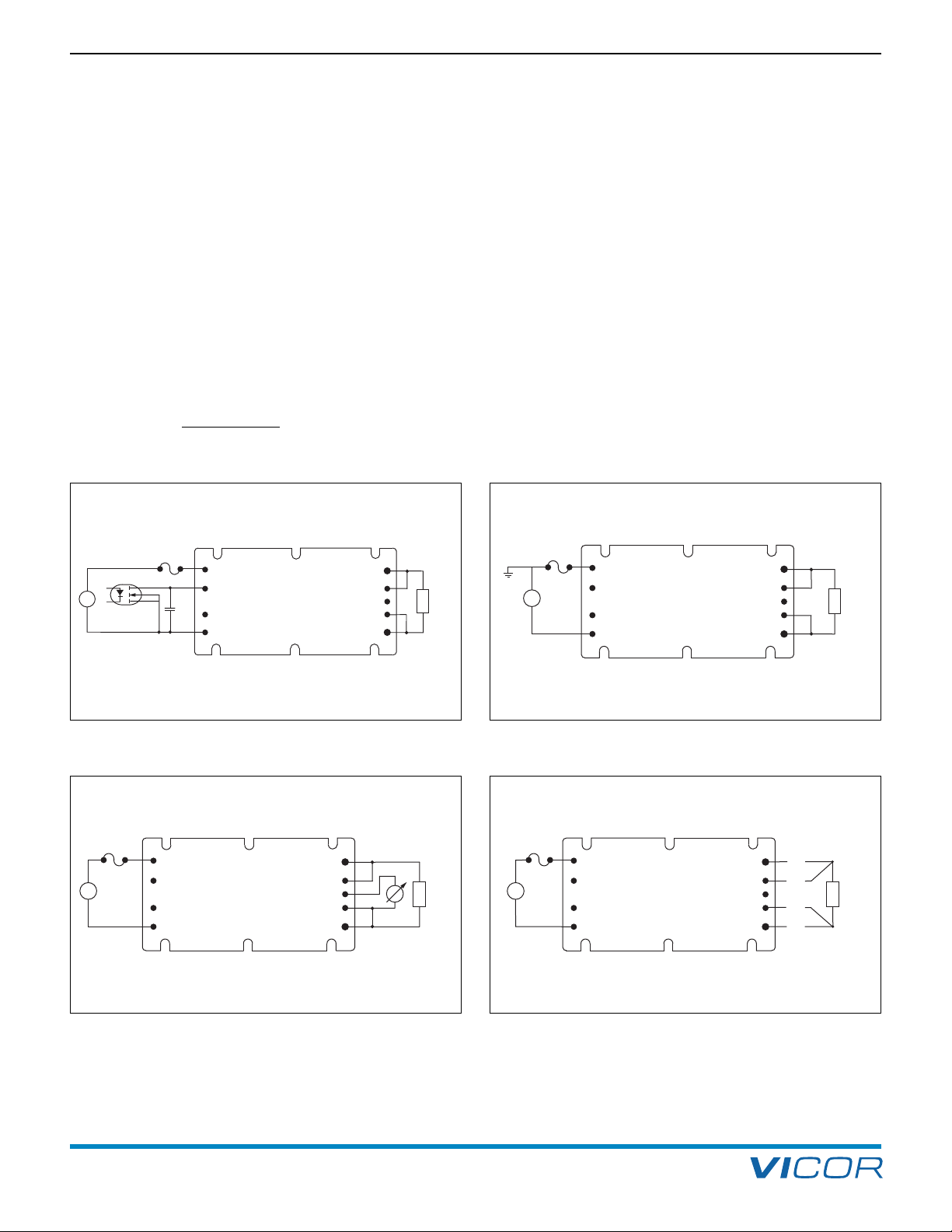
Logic Disable. (Figure 7–1) The GATE IN pin of the
module may be used to turn the module on or off. When
GATE IN is pulled low (<0.65 V @ 6 mA, referenced to
Vin), the module is turned off. When GATE IN is floating
–
(open collector), the module is turned on. The open circuit
oltage of the GATE IN pin is less than 10 V. This applies
v
to VI-/ MI-200, VI-/MI-J00 and MegaMod / MI-MegaMod
Family modules.
Output Voltage Programming. (Figure 7–2) Consult
Vicor’s Applications Engineering Department before
attempting large signal applications at high repetition
rates due to ripple current considerations with the internal
output capacitors. This applies to VI-/ MI-200, VI-/MI-J00,
ComPAC /MI-ComPAC, FlatPAC and MegaMod/
MI-MegaMod Family modules.
Vout =
Vtrim x Vnom
2.5
Negative Inputs (with positive ground). (Figure 7–3)
Vicor modules have isolated inputs and outputs making
negative input configurations easy. Fusing should always
e placed in the positive lead.
b
Remote Sensing. (Figure 7–4) Output voltage between
+OUT and –OUT must be maintained below 110% of
nominal. Do not exceed 0.25 V drop in negative return as
the current limit setpoint is moved out proportionately.
The sense should be closed at the module if remote
sensing is not desired. Applies to VI-/ MI-200, VI-/ MI-J00,
ComPAC /MI-ComPAC, FlatPAC and MegaMod/
MI-MegaMod Family modules. Excessively long sense leads
and / or excessive external capacitance at the load may
result in module instability. Please consult Vicor
Applications Engineering for compensation methods.
Figure 7–1 — Logic disable
Figure 7–2 — Output voltage programming
VI-200 and VI-J00 Family Design Guide Rev 3.5 vicorpower.com
Page 12 of 98
Apps. Eng. 800 927.9474 800 735.6200
Figure 7–3 — Negative inputs (with positive ground)
Figure 7–4 — Remote sensing
Page 14
Design Guide & Applications Manual
–OUT
–S
T
RIM
+S
+OUT
+IN
GATE
IN
GATE
O
UT
–IN
Zero Current
S
witching
C
onverter
#1
Driver
VI-2xx-xx
+
–
–OUT
–S
TRIM
+S
+OUT
+IN
GATE
IN
GATE
OUT
–IN
Zero Current
Switching
Converter
#n
Booster
VI-Bxx-xx
Load
–OUT
-S
TRIM
+S
+OUT
+IN
GATE
IN
GATE
OUT
–IN
Zero Current
Switching
Converter
Driver
+
–
Load
V Control
0.1 V/A
1K
OP
AMP
–
+
1K
1K
0.05 Ω
1K
0.01
I
10 µF
–OUT
–S
TRIM
+S
+OUT
+IN
GATE
IN
GATE
OUT
–IN
Zero Current
Switching
Converter
Driver
+
–
Load requiring
positive output
–OUT
–S
T
RIM
+S
+OUT
+
IN
GATE
IN
GATE
OUT
–IN
Z
ero Current
S
witching
C
onverter
Driver
+
–
Load requiring
negative output
or VI-200 and VI-J00 Family DC-DC Converters and Configurable Power Supplies
F
7. Application Circuits / Converter Array Design Considerations
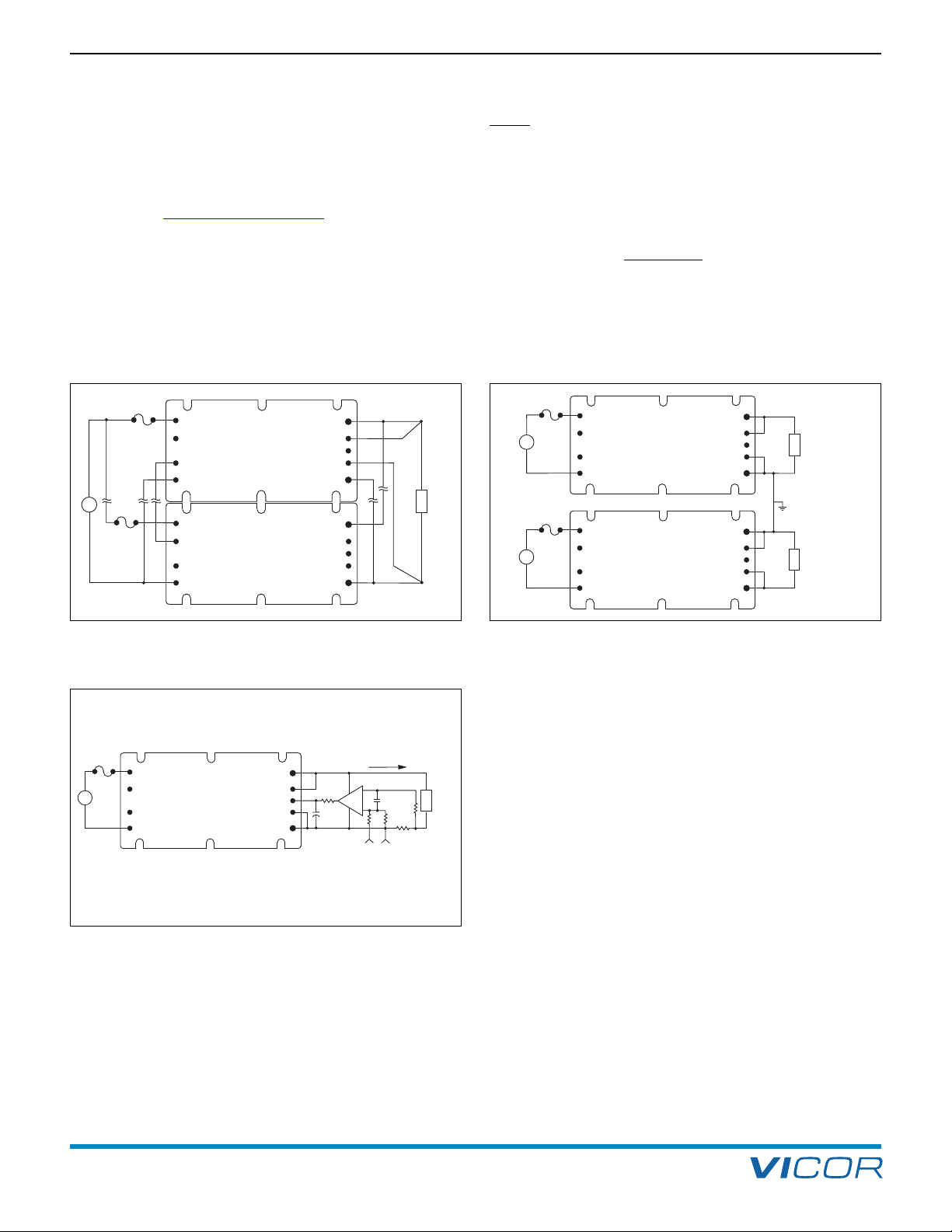
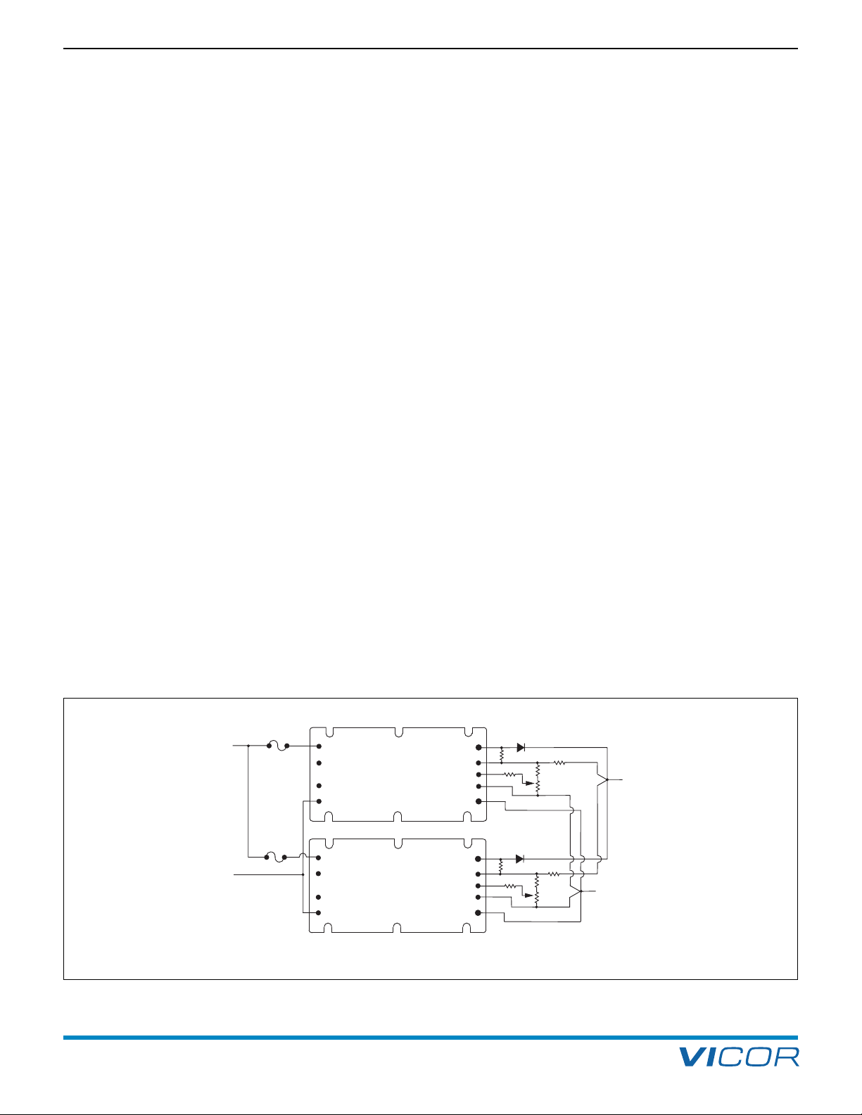
Parallel Boost. (Figure 7–5) U.S. Patent #4,648,020 —
other patents pending. To retain accurate power sharing
between a Driver and (n) number of Boosters, provide
dequate input and output power bussing. This applies to
a
VI-/MI-200 and MegaMod / MI-MegaMod Family
odules. See
m
odule Do’s and Don’tsfor recommended
M
external components. (Section 3)
Programmable Current Source. (Figure 7–6) Module
output voltage should not exceed the rated voltage of the
operational amplifier. This applies to VI-/ MI-200,
VI-/MI-J00, ComPAC/ MI-ComPAC, FlatPAC and
MegaMod/MI-MegaMod Family modules.
: When using a VI-J00 module, the TRIM pin
NOTE
voltage should be clamped to 2.75 V to avoid
damage to the module. This corresponds to the
aximum trim up voltage. This circuit or functional
m
equivalent must be used when charging batteries.
o not exceed the nominal current ratings of the
D
converter. Example,
Pout
Vnominal
Dual Output Voltages. (Figure 7–7) Vicor modules have
isolated outputs so they can easily be referenced to a
common node creating positive and / or negative rails.
Figure 7–5 — Parallel boost. U.S. Patent #4,648,020 — other
Figure 7–7 — Dual output voltages
patents pending.
Figure 7–6 — Programmable current source
VI-200 and VI-J00 Family Design Guide Rev 3.5 vicorpower.com
Page 13 of 98
Apps. Eng. 800 927.9474 800 735.6200
Page 15
INPUT
LOAD
+S
TRIM
–S
–OUT
+IN
GATE
IN
GATE
OUT
–IN
+S
TRIM
–S
–OUT
+IN
GATE
IN
GATE
OUT
–IN
+S
TRIM
–S
–OUT
+IN
GATE
IN
GATE
OUT
–IN
+
–
Zero-Current-
Switching
Driver
VI-2xx-xx
Zero-Current-
Switching
Booster
VI-Bxx-xx
Zero-Current-
Switching
Booster
VI-Bxx-xx
+OUT
+OUT
+OUT
8. Using Boosters and Parallel Arrays
or VI-200 and VI-J00 Family DC-DC Converters and Configurable Power Supplies
F
Design Guide & Applications Manual
OVERVIEW
The VI-/MI-200 Family of DC-DC converters are available
as Driver or Booster modules. The Driver can be used as a
stand alone module, or in multi-kilowatt arrays by adding
parallel Boosters. Booster modules do not contain
feedback or control circuitry, so it is necessary to connect
the Booster GATE IN pin to the preceding Driver or
Booster GATE OUT, to synchronize operation. Drivers and
Boosters have identical power trains, although Drivers
close the voltage loop internally while Boosters do not.
The concept behind Driver / Booster operation is that two
or more ZCS power trains driven at the same frequency
will inherently load-share if their inputs and outputs are
tied together. Slaved modules require only one connection
between units when their outputs are connected
together; no trimming, adjustments or external
components are required to achieve load sharing. The
load sharing is dynamic and typically within 5%.
For additional information, refer to Electrical Considerations
– High Power Arrays in the Module Do’s and Don’ts.
(Section 3)
IMPORTANT: It is important to remember that when
using Boosters, the input voltage, output voltage and
output power of the Boosters must be the same as
the Driver.
Whenever power supplies or converters are operated in a
parallel configuration—for higher output power, fault
tolerance, or both—current sharing is an important
consideration. Most current-sharing schemes employed
with power converters involve analog approaches. One
analog method artificially increases the output impedance
f the converter modules, while another actually senses
o
the output current of each module and forces all of the
urrents to be equal by feedback control.
c
Synchronous current sharing offers an alternative to
analog techniques. In a synchronous scheme, there is no
need for a current-sensing or current-measuring device on
each module. Nor is there a need to artificially increase
output impedance, which compromises load regulation.
There are advantages and disadvantages associated with
each approach to current sharing. In choosing the best
approach for a given application, designers should be
aware of the tradeoffs as well as tips for implementing a
successful design.
Most paralleled power components, such as transistors,
rectifiers, power conversion modules, and offline power
supplies, will not inherently share the load. With power
converters, one or more of the converters will try to
assume a disproportionate or excessive fraction of the
load unless forced current-sharing control is designed into
the system.
One converter, typically the one with the highest output
voltage, may deliver current up to its current limit setting,
which is beyond its rated maximum. Then, the voltage will
drop to the point where another converter in the array—
the one with the next highest voltage—will begin to
deliver current. All of the converters in an array may
Figure 8–1 — Parallel array
VI-200 and VI-J00 Family Design Guide Rev 3.5 vicorpower.com
Page 14 of 98
Apps. Eng. 800 927.9474 800 735.6200
Page 16

Design Guide & Applications Manual
or VI-200 and VI-J00 Family DC-DC Converters and Configurable Power Supplies
F
8. Using Boosters and Parallel Arrays
deliver some current, but the load will be shared unequally.
With built-in current limiting, one or more of the converters
will deliver current up to the current limit (generally 15 or
0% above the module’s rated maximum), while other
2
converters in the array supply just a fraction of load.
Consider a situation where one module in a two-module
array is providing all of the load. If it fails, the load on the
second module must go from no load to full load. During
that time, the output voltage is likely to droop temporarily.
This could result in system problems, including shutdown
or reset.
On the other hand, if both modules were sharing the load
and one failed, the surviving module would experience a
much less severe transient (one-half to full load). Also, the
output voltage would be likely to experience no more
than a slight momentary droop. The dynamic response
characteristic of all forward converters, resonant or pulsewidth modulated, is degraded when the load is stepped
from zero (no load) where the output inductor current is
discontinuous.
In the same two-module array example, the module
carrying all of the load also is generating all of the heat.
That results in a much lower mean time between failure
for that module. An often-quoted rule of thumb says that
for each 10°C increase in operating temperature, average
component life is cut in half.
In a current-sharing system, the converters or supplies all
run at the same temperature. This temperature is lower
than that of the hot-running (heavily loaded) modules in
a system without current sharing. Furthermore, sametemperature operation means that all of the modules in
a current-sharing arrangement age equally.
Current sharing, then, is important because it improves
system performance. It optimizes transient and dynamic
response and minimizes thermal problems, which improves
reliability and helps extend the lifetimes of all of the
modules in an array. Current sharing is an essential
ingredient in most systems that use multiple power supplies
or converters to achieve higher output power or fault
tolerance.
When parallel supplies or converters are used to increase
power, current sharing is achieved through a number of
approaches. One scheme simply adds resistance in series
with the load. A more practical variant of that is the
“droop-share” method, which actively causes the output
voltage to drop in response to increasing load.
Nevertheless, the two most commonly used approaches
to paralleling converters for power expansion are Driver /
Booster arrays and analog current-sharing control. They
appear to be similar, but the implementation of each is
quite different.
Driver / Booster arrays usually contain one intelligent
module or Driver, and one or more power-train-only
modules or Boosters. Analog current-sharing control
nvolves paralleling two or more identical modules, each
i
containing intelligence.
One of the common methods of forcing load sharing in
an array of parallel converters is to sense the output
current of each converter and compare it to the average
current. Then, the output of a given converter is adjusted
so that its contribution is equal to the average. This is
usually accomplished by current-sense resistors in series
with the load, a sensing amplifier for each converter
module, and a summing amplifier. Load sharing is
accomplished by actively trimming the output voltage
using TRIM or SENSE pins.
Occasionally, a designer is tempted to avoid the expense
of a current-sense resistor by using the IR drops in the
wire as a means of sensing the current. Unfortunately,
there are a number of negative issues associated with
that idea. First of all, there’s the temperature coefficient
of copper. As the wire heats up, its resistance increases,
negating its value as a stable current-sensing device.
Second, there are oxidation and corrosion issues, which
also cause parametric changes. Consequently, a highprecision current-sensing device, such as a precision
resistor, is a must.
The resistor values typically range from a few milliohms
up to about 100 mΩ, depending on the power level or
current range of operation. Selecting the right value
requires a tradeoff between power dissipation and
sensitivity (signal-to-noise ratio or noise immunity). The
larger the resistor value, the better the noise immunity—
and the greater the power dissipation.
Determining the size of the resistor needed to generate a
signal above the noise can be a bit tricky. Another
potential pitfall with this (or, for that matter, any other)
approach is the need for good electrical and mechanical
design and layout. This requires adequate trace widths,
minimized trace lengths, and decoupling to reduce noise.
An experienced designer should have no difficulty with
this, but it is an area rich with opportunities for error.
The droop-share method artificially increases the output
impedance to force the currents to be equal.
It’s accomplished by injecting an error signal into the
control loop of the converter, causing the output voltage
to vary as a function of load current. As load current
increases, output voltage decreases. All of the modules
will deliver approximately the same current because they
are all being summed into one node.
If one supply is delivering more current than another
supply, its output voltage will be slightly forced down so
VI-200 and VI-J00 Family Design Guide Rev 3.5 vicorpower.com
Page 15 of 98
Apps. Eng. 800 927.9474 800 735.6200
Page 17
–OUT
–S
TRIM
+S
+OUT
+IN
GATE
IN
GATE
OUT
–IN
–OUT
–S
TRIM
+S
+OUT
+IN
GATE
IN
GATE
OUT
–IN
Return
Zero Current
Switching
Converter
#1
Driver
Zero Current
Switching
Converter
#n
Driver
+V
IN
+V
OUT
–V
IN
8. Using Boosters and Parallel Arrays
or VI-200 and VI-J00 Family DC-DC Converters and Configurable Power Supplies
F
Design Guide & Applications Manual
that it will be delivering equal current for an equal voltage
at the summing node. A simple implementation of the
droop-share scheme uses the voltage dropped across an
Ring diode, which is proportional to current, to adjust
O
the output voltage of the associated converter. (Figure 8–2)
Droop share has advantages and disadvantages. One of
the advantages is that it can work with any topology. It’s
also fairly simple and inexpensive to implement. Though, a
major drawback is that it requires that the current be
sensed. A current-sensing device is needed in each of the
converters or power supplies. Additionally, a small penalty
is paid in load regulation, though in many applications this
isn’t an issue.
In general, mixing and matching converters isn’t
recommended—especially those with incompatible
current-sharing schemes. The droop-share method,
however, is more forgiving in this regard than any of the
other techniques. With a little external circuitry, current
sharing can be achieved using arrays constructed from
different converter models or even from different suppliers.
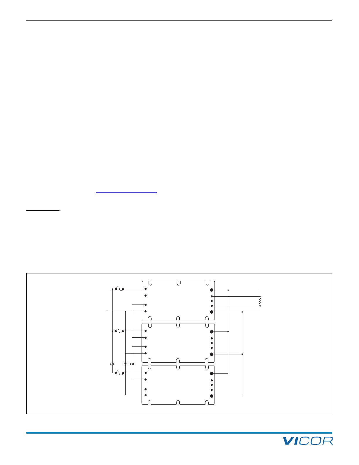
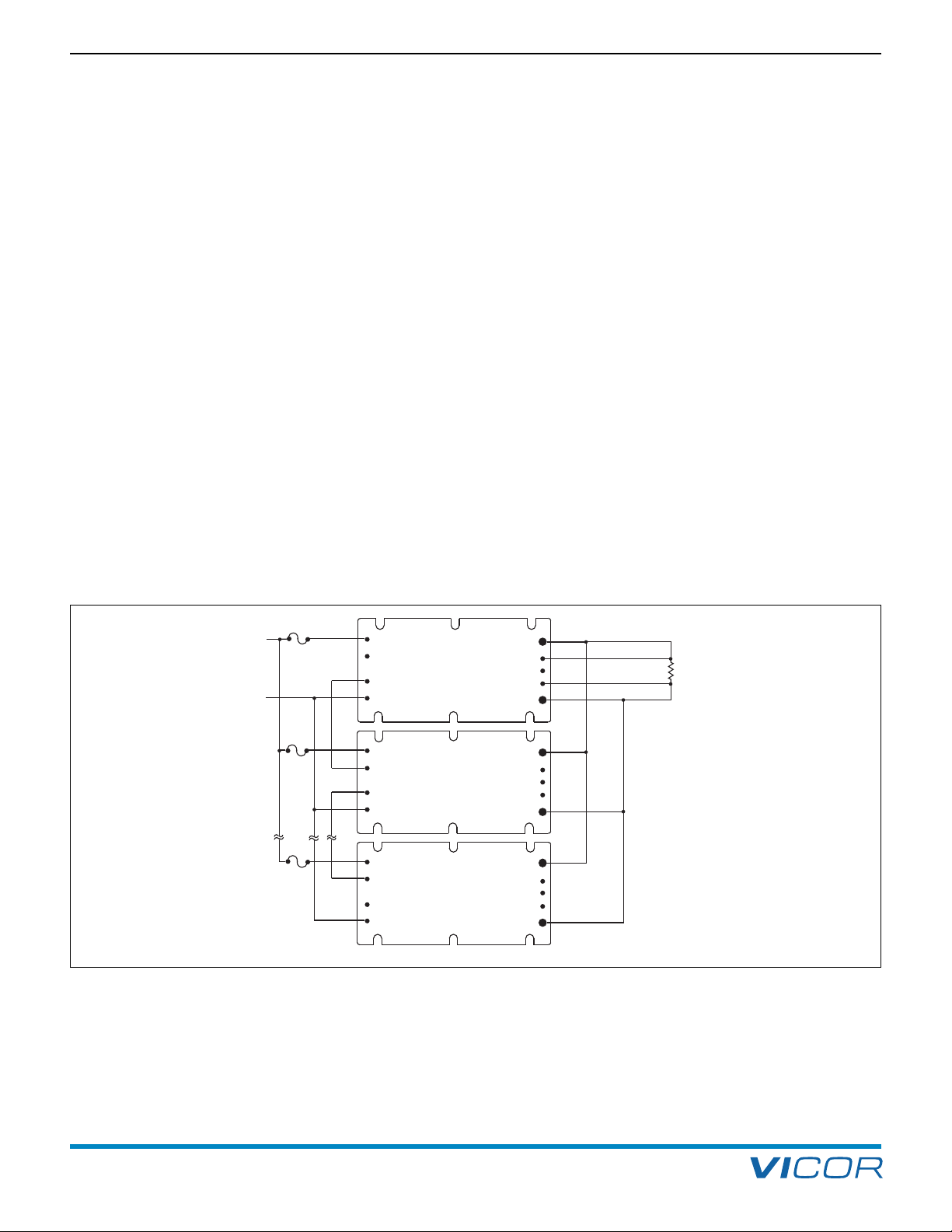
Most systems can employ the Driver / Booster (or master /
slave) array for increased power. (Figure 8–3) The Driver is
used to set and control output voltage, while Booster
modules, as slaves to the master, are used to extend
output power to meet system requirements.
Driver / Booster arrays of quasi-resonant converters with
identical power trains inherently current share because the
per-pulse energy of each converter is the same. If the
inputs and outputs are tied together and the units operate
at the same frequency, all modules will deliver equal
current (within component tolerances).
The single intelligent module in the array determines the
transient response, which does not change as modules
are added. Slaved modules require only one connection
etween units when their outputs are connected. No
b
trimming, adjustments, or external components are
equired to achieve load sharing. The load sharing is
r
dynamic and usually guaranteed within 5%. It’s important
to remember that when using Boosters, the input and
output voltage and output power specifications of the
Boosters must be the same as the Driver.
Driver / Booster arrays have two advantages. They have
only a single control loop, so there are no loop-within-aloop stability issues. And, they have excellent transient
response. However, this arrangement isn’t fault tolerant.
If the Driver module fails, the array won’t maintain its
output voltage.
Analog current-sharing control involves paralleling two or
more identical modules, each containing intelligence. The
circuit actively adjusts the output voltage of each supply
so the multiple supplies deliver equal currents. This method,
though, has a number of disadvantages. Each converter in
the array has its own voltage regulation loop, and each
requires a current-sensing device and current-control loop.
Analog current-sharing control does support a level of
redundancy. But it’s susceptible to single-point failures
within the current-sharing bus that at best can defeat
current sharing, and at worst can destroy every module in
the array. The major reason for this is the single-wire
galvanic connection between modules.
Current sharing is an essential element in fault-tolerant
arrays. Yet regardless of the approach, there is an inherent
Figure 8–2 — Droop-share current sharing artificially increases converter output impedance to force the currents to be equal. Diodes on the
output of each converter provide current sensing and fault protection.
VI-200 and VI-J00 Family Design Guide Rev 3.5 vicorpower.com
Page 16 of 98
Apps. Eng. 800 927.9474 800 735.6200
Page 18
Design Guide & Applications Manual
INPUT
LOAD
+ Sense
T
rim
–Sense
GATE
IN
–
IN
Zero-Current-
Switching Driver
+
OUT
GATE
OUT
+IN
–OUT
+Sense
Trim
–Sense
–IN
Zero-Current-
Switching Booster
+OUT
+IN
–OUT
+Sense
Trim
–Sense
–IN
Zero-Current-
Switching Booster
+OUT
+IN
–OUT
+V
I
N
-V
IN
GATE
IN
GATE
OUT
GATE
IN
GATE
OUT
or VI-200 and VI-J00 Family DC-DC Converters and Configurable Power Supplies
F
8. Using Boosters and Parallel Arrays
cost incurred by the addition of at least one redundant
onverter or supply.
c
ncidentally, most applications today that require fault
I
tolerance or redundancy also require Hot-Swap capability
to ensure continuous system operation. Hot-swappable
cards must be designed so the operator won’t come in
contact with dangerous potentials and currents.
It’s also essential that when a module fails, the failure is
detected and identified by an alarm or notice to provide
service. A Hot-Swap system must ensure that during
swap-out, there is minimal disturbance of the power bus.
Specifically, the affected voltage bus must not drop
enough to cause errors in the system, either on the input
bus or the output bus.
A power-supply failure can cripple an entire system, so the
addition of a redundant converter or supply is often
justified by the need to keep the system operating.
Adding an extra module (N+1) to a group of paralleled
modules will significantly increase reliability with only a
modest increase in cost.
The implementation of redundant converters is
determined in part by the available space and cost
requirements. For example, two 200 W full-size modules
could be used to provide a 400 W output with an
dditional 200 W module for 2+1 redundancy (a total of
a
600 W in a volume of about 16.5 in
3
).
Alternatively, four 100 W half-size modules might be used
with a fifth 100 W module to provide 4+1 redundancy (a
total of 500 W and 14 in3). Although the second solution
uses less space, it increases the accumulated failure rate
because it employs more converters, more ORing diodes,
more monitoring circuitry, and more assembly.
ORing diodes may be inserted in series with the output
of each module in an N+1 array to provide output fault
tolerance. (Figure 8–2) They’re important in a redundant
power system to maintain fault isolation. Without them,
a short-circuit failure in the output of one converter could
bring down the entire array.
But ORing diodes add losses to the power system,
reducing overall efficiency and decreasing reliability. To
ameliorate the negative effect on efficiency, ORing diodes
should run hot, thereby reducing forward voltage drop
and increasing efficiency. Reverse leakage current will be
an issue only if the output of a converter shorts and the
diode is reverse biased. This is an important consideration
with regard to operating temperature.
Figure 8–3 — Most converters can use the Driver / Booster array to increase output power. Driver / Booster arrays usually contain one
intelligent module or Driver, and one or more power-train-only modules or Boosters.
VI-200 and VI-J00 Family Design Guide Rev 3.5 vicorpower.com
Page 17 of 98
Apps. Eng. 800 927.9474 800 735.6200
Page 19
+IN
GATE
IN
GATE
OUT
–IN
+OUT
+S
TRIM
–S
–OUT
C2
C1
C2
C3
C3
C1 = 100 µF
C2 = 4,700 pF
C3 = 0.01 µF
Conditions:
Light Load = 3 A
Nominal Line = 48 V Nominal Load = 15 A
Full Load = 30 A
9. EMC Considerations
or VI-200 and VI-J00 Family DC-DC Converters and Configurable Power Supplies
F
Design Guide & Applications Manual
CONDUCTED NOISE
Conducted noise is the AC current flowing between the
source voltage and the power supply. It includes both
common-mode and differential-mode noise. Vicor zero-
urrent-switching converters are 20 – 40 dB lower in
c
conducted noise than a traditional board-mounted PWM
converter; however, if a specific EMC specification such as
FCC or VDE must be met, additional filtering may be required.
Since the noise generated is ten to a hundred times lower
than fixed frequency converters, an existing filter should
provide equal or better performance when the conditions
in the Module Do’s and Don’ts section are followed.
(Section 3)
In the event the system does not contain an existing filter,
the following will provide valuable information relative to
the attainment of system conducted noise objectives.
System requirements, such as Tempest (military) or UL544/
EN60601 (medical), require a somewhat different approach.
Medical requirements vary as a function of the application
and country — please contact Vicor Applications
Engineering for additional details.
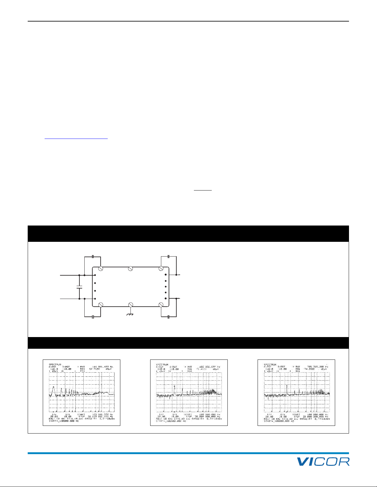
Common-Mode Noise with No Additional Filtering.
Common mode conducted noise current is the
unidirectional (in phase) component in both the +IN and
–IN pins to the module. This current circulates from the
converter via the power input leads to the DC source and
returns to the converter via the grounded baseplate or
output lead connections. This represents a potentially
large loop cross-sectional area which, if not effectively
controlled, can generate magnetic fields. Common-mode
noise is a function of the dv/dt across the main switch in
the converter and the effective input to baseplate and
input to output capacitance of the converter.
The most effective means to reduce common-mode current
is to bypass both input leads to the baseplate with
Y-capacitors (C2), keeping the leads short to reduce
parasitic inductance. Additionally, a common-mode choke
(L1) is usually required to meet FCC/ VDE A or B. (Figure
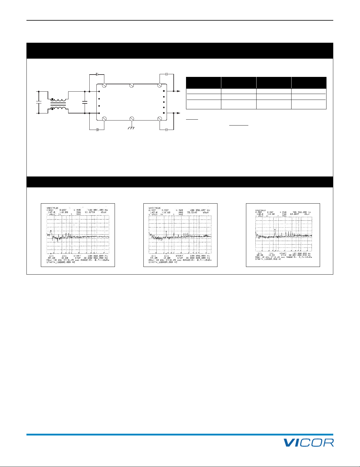
9–2)
NOTE:
Acoustic Noise. Audible noise may be emitted
from the module under no load, light load, or
dynamic loading conditions. This is considered
normal operation of the module.
Typical Vicor Module
48 V Input, 5 V Output (VI-230-CV)
Conducted Noise vs. Load
3 Amp Load 15 Amp Load 30 Amp Load
Figure 9–1 — Conducted input noise, no additional filtering
VI-200 and VI-J00 Family Design Guide Rev 3.5 vicorpower.com
Page 18 of 98
Apps. Eng. 800 927.9474 800 735.6200
Page 20
Design Guide & Applications Manual
+IN
–IN
+OUT
–
OUT
C1 = 2.2 µF
C2 = 100 µF
C3 = Internal
C4 = Internal
L1 = 3 mH
Conditions:
L
ight Load = 3 A
Nominal Load = 15 A
Full Load = 30 A
C1
L1
C
2
C3
C3
C4
C4
Nominal Line = 48 V
C
M
or VI-200 and VI-J00 Family DC-DC Converters and Configurable Power Supplies
F
9. EMC Considerations
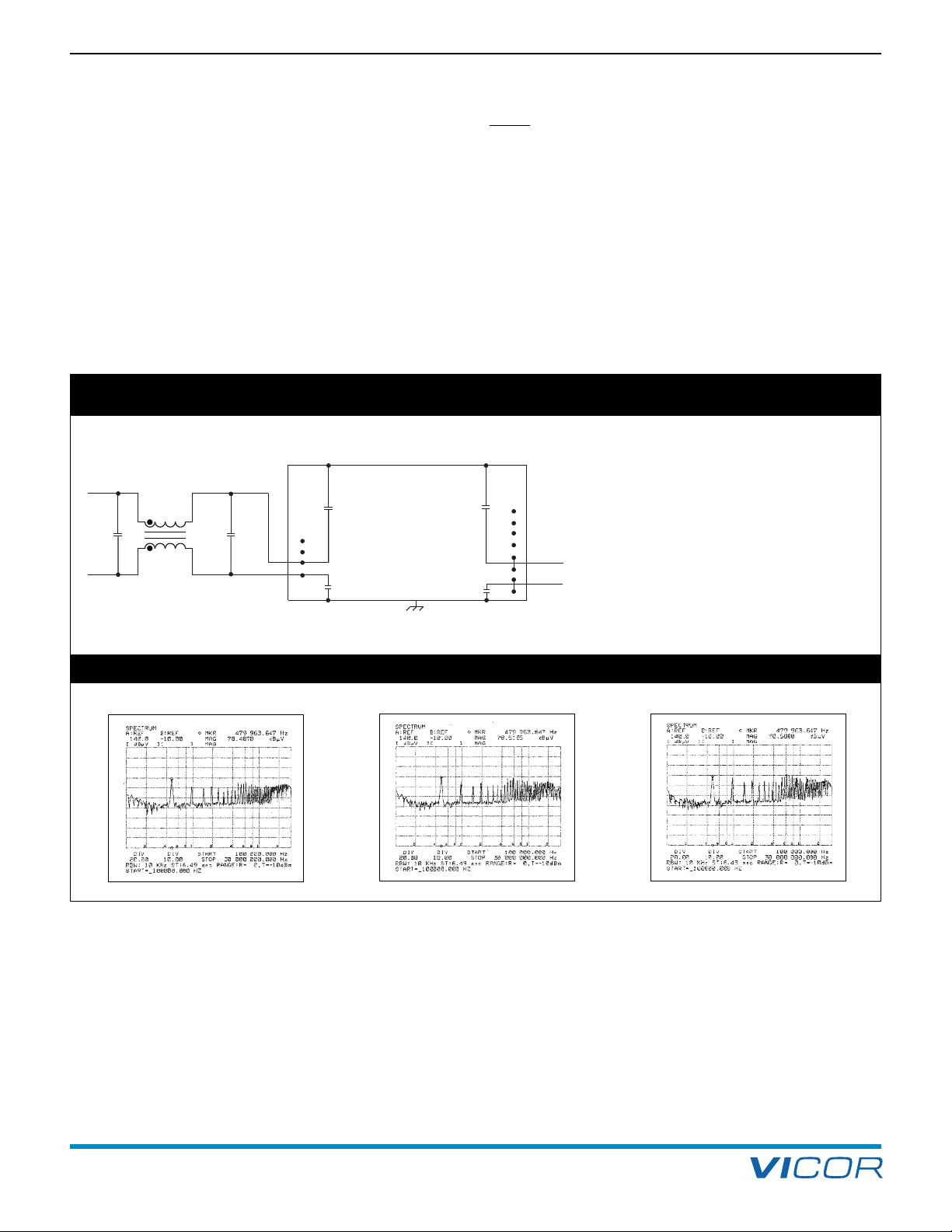
Common-Mode Noise with Common-Mode Choke.
There are no special precautions that must be exercised in
the design of input filters for Vicor converters. In fact, if
he system contains an EMC filter designed for typical
t
fixed frequency converters, it should be sufficient as is
although not optimal in terms of size), as zero-current-
(
switching converters inherently generate significantly less
conducted noise.
The plots in Figure 9–2 are representative of fixed
frequency converters with input filtering.
Typical Fixed Frequency Converter (PWM)
48 V Input, 5 V Output
: In most cases, a fixed frequency converter
NOTE
generates more input conducted noise with a filter
than Vicor’s zero-current-switching converter without
filter. Also note that fixed frequency converters
a
using a construction technique involving control
ircuitry on the same metal plate as power processing
c
components will generate significantly more input
noise than shown.
Conducted Noise vs. Load
3 Amp Load 15 Amp Load 30 Amp Load
Figure 9–2 — Conducted input noise, typical fixed frequency converter with filter
VI-200 and VI-J00 Family Design Guide Rev 3.5 vicorpower.com
Page 19 of 98
Apps. Eng. 800 927.9474 800 735.6200
Page 21
9. EMC Considerations
C
4
C1 = 100 µF
C2
a –
C
2
b
= 4,700 pF (Vicor Part # 01000)
C3
a
–
C3
b
= 0.01 µF
(Vicor Part # 04872)
C4 = 2.2
µF
L1 = 3,000
µH
(Vicor Part # 31742)
Conditions
L
ight Load = 3 A
Nominal Load = 15 A
Full Load = 30 A
+IN
GATE
I
N
GATE
OUT
–IN
+
OUT
+
S
T
RIM
–
S
–OUT
C
2
a
C
1
C
2
b
C
3
b
C
3
a
L1
CM
or VI-200 and VI-J00 Family DC-DC Converters and Configurable Power Supplies
F
Typical Vicor Module (VI-230-CV)
48 V Input, 5 V Output
Three common-mode chokes are offered as standard accessories.
Part Inductance Maximum Resistance
Number Each Winding DC Current Each Winding
31743 1,000 µH 12 Amperes 6.5 mΩ
31742 3,000 µH 7 Amperes 18 mΩ
31943 2,163 µH 1 Ampere 42 mΩ
: Common-mode filters may be common to one or
NOTE
more modules, but only one
interconnected via GATE IN’s or, GATE OUT to GATE IN. As
an example, Driver / Booster arrays or Drivers with GATE IN’s
tied together to provide a common disable function.
Conducted Noise vs. Load
Design Guide & Applications Manual
should be used with modules
3 Amp Load 15 Amp Load 30 Amp Load
Figure 9–3 — Conducted input noise, with common-mode choke
VI-200 and VI-J00 Family Design Guide Rev 3.5 vicorpower.com
Page 20 of 98
Apps. Eng. 800 927.9474 800 735.6200
Page 22
Design Guide & Applications Manual
+IN
GATE
IN
G
ATE
OUT
–IN
+OUT
+S
T
–S
–OUT
Load 1
Load 2
L
2
C4
L1
C1
a
C
2
a
C2
d
C2
c
C2
b
C3
a
C3
b
C3
c
C3
d
C1
b
+IN
GATE
IN
GATE
OUT
–IN
+OUT
+S
T
–S
–OUT
C1a – C1b = 47 µF
C2a – C2d = 4,700 pF (Vicor Part # 01000)
C3a – C3d = 0.01 µF (Vicor Part # 04872)
C4 = 2.2 µF
L1 = 3,000 µH (Vicor Part # 31742)
L2 = 20 µH
C
onditions
Light Load = 3 A
Nominal Load = 15 A
Full Load = 30 A
CM
or VI-200 and VI-J00 Family DC-DC Converters and Configurable Power Supplies
F
9. EMC Considerations
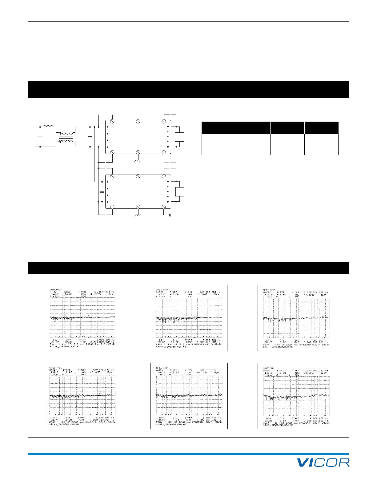
Differential and Common-Mode Filter with More
than One Module. No special precautions are needed
when using two or more modules. The filter required will
ave the same characteristics as a single module filter,
h
Differential and Common-Mode Filter with More than One Module
48 V Inputs, 5 V Outputs (Two Vicor VI-230-CV Modules)
however the wire size on the magnetics will need to
reflect the increased input current. Shown below is the
input conducted noise for two modules sharing a
ommon input source.
c
Three common-mode chokes are offered as standard accessories.
Part Inductance Maximum Resistance
Number Each Winding DC Current Each Winding
31743 1,000 µH 12 Amperes 6.5 mΩ
31742 3,000 µH 7 Amperes 18 mΩ
31943 2,163 µH 1 Ampere 42 mΩ
: Common-mode filters may be common to one or
NOTE
more modules, but only one should be used with modules
interconnected via GATE IN’s or, GATE OUT to GATE IN. As
an example, Driver / Booster arrays or Drivers with GATE IN’s
tied together to provide a common disable function.
Conducted Noise vs. Load
3 Amp / 3 Amp Load
15 Amp / 15 Amp Load
Figure 9–4 — Conducted noise, multiple zero-current-switching converters
3 Amp / 6 Amp Load
3 Amp / 30 Amp Load
15 Amp / 30 Amp Load 30 Amp / 30 Amp Load
VI-200 and VI-J00 Family Design Guide Rev 3.5 vicorpower.com
Page 21 of 98
Apps. Eng. 800 927.9474 800 735.6200
Page 23
9. EMC Considerations
C2
a
C
1
C2
b
C3
b
C3
a
L1
C
4
L2
C1 = 100 µF
C 2a – C2b = 4,700 pF (Vicor Part # 01000)
C 3a – C3b = 0.01 µF (Vicor Part # 04872)
C4 = 2.2 µF
L1 = 20 µH
L2 = 20 µH
+
IN
GATE
IN
GATE
OUT
–IN
+OUT
+S
T
RIM
–
S
–OUT
C
onditions
Light Load = 3 A
Nominal Load = 15 A
Full Load = 30 A
or VI-200 and VI-J00 Family DC-DC Converters and Configurable Power Supplies
F
Design Guide & Applications Manual
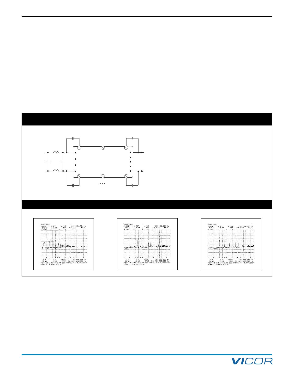
Differential-Mode Noise Filter. Differential-mode
conducted noise current is the component of current,
at the input power pin, which is opposite in direction or
hase with respect to the other input power pin.
p
All Vicor converters have an internal differential-mode LC
filter which, in conjunction with a small external capacitor
C1 (minimum value in µF) = 400 / Vin,
reduces differential-mode conducted noise. The external
capacitor should be placed close to the module to reduce
loop cross-sectional area.
Differential-Mode Filter
Typical Vicor Module (VI-230-CV) 48 V Input, 5 V Output
Care should be taken to reduce the loop cross-sectional
area of differential-mode current flowing between the
source and C1. Since differential-mode input current is by
efinition opposite in phase, twisting the input leads
d
causes noise cancellation. PCB power planes can reduce
adiated noise if the traces are on opposite sides of the
r
PCB directly over one another. If differential mode inductance
is used, it may be common to one or more modules.
Conducted Noise vs. Load
3 Amp Load 15 Amp Load 30 Amp Load
Figure 9–5 — Conducted noise, differential-mode filtering
VI-200 and VI-J00 Family Design Guide Rev 3.5 vicorpower.com
Page 22 of 98
Apps. Eng. 800 927.9474 800 735.6200
Page 24

L
C
Vs
Ip
+IN
–IN
Vp
+
OUT
–
OUT
Ceramic
Parasitic
Capacitance
Baseplate
Rectifier
Ceramic
FET
ShieldShield
Design Guide & Applications Manual
or VI-200 and VI-J00 Family DC-DC Converters and Configurable Power Supplies
F
RADIATED NOISE
Radiated noise may be either electric field or magnetic
field. Magnetic radiation is caused by high di/dt and is
generally what is measured by FCC, VDE or MIL-STD-461.
Vicor converters utilize zero-current-switching, with the
advantage over PWM non-zero-current-switching being
that zero-current-switching topologies contain minimal
discontinuities in the switched current waveforms,
resulting in lower di/dt’s. Electric field radiation (caused by
dv/dt) is “near-field,” i.e., it decays rapidly as a function of
distance and as a result does not typically affect radiated
measurements.
Figure 9–6 — Basic zero-current-switching converter topology
Radiation can be minimized by proper board layout. Keep
(VI-200 / VI-J00)
all leads with AC current short, twisted or routed as
overlapping planes to minimize loop cross-sectional area.
Also keep in mind the effects of capacitive coupling —
even when not expected. Do not put an unshielded filter
on the opposite side of the PCB from the module.
Conducted noise can be capacitively coupled around the
filter. Do not route input and output leads in the same
cable bundle. Again, no special precautions, just good
design practice.
Since the energy in every pulse is related to the square of
the applied voltage (CV
as approximately the square of the line voltage. For
example, a 300 V input unit can vary from 200 – 400 V,
or a factor of two, therefore it follows that the repetition
rate must vary by approximately a factor of four to regulate
the output. As previously established, the current in the
primary is a half-wave rectified sine wave, but the voltage
on the primary is a square wave. Since this voltage is a
square wave, it contains harmonics of the fundamental
NOISE CONSIDERATIONS
switching frequency. It also includes frequencies, that extend
to 70 MHz.
All switchmode power supplies generate a certain amount
of “noise”, yet it remains one of the least understood
parameters in power conversion.
These frequencies can be of interest in the following
circumstances. Rapidly changing voltages (high dv/dt) can
generate E-fields (primarily near-field) which do not usually
VI-200s and VI-J00s both use the same topology, so their
operation is very similar. These products are zero-currentswitching converters — i.e., the current is zero when the
main switch is turned on or off. While the switch is on,
the current through the switch or the primary of the
transformer is a half-wave rectified sine wave. Similar in
operation to a resonant converter, these products are
commonly referred to as quasi-resonant converters. The
LC resonant frequency is fixed so the on-time of the
switch is about 500 ns. When the switch turns on, energy
builds up in the leakage inductance of the transformer (L)
and then “transferred” into the capacitor on the
secondary side of the module. (C, Figure 9–6) The energy
processed in each pulse is fixed, and is ultimately the
2
energy stored in this capacitor, 1/2 CV
. Since the energy
cause system noise problems since they significantly
decrease as a function of distance. For this reason, E-fields
are not measured by agencies such as the FCC or VDE.
These agencies do, however, measure the magnetic
radiation caused by high frequency currents in a conductor.
The half-wave rectified sine wave in the transformer is an
example of this, but since there are minimal discontinuities
in the current waveform and the loop cross-sectional area
is very small, the resultant E-field is very small. E-fields can
be a problem if sensitive circuitry is located near the
module. In this case, a shield can be positioned under the
label side of the module as a discrete element or as a
ground plane on the PCB. The other effect that occurs as
a result of the 50 – 70 MHz component on the main
switch is common-mode noise. (Figure 9–7)
in every pulse is fixed, the repetition rate of the pulse train
is varied as a function of load to regulate the output
voltage. Maximum repetition rate occurs at minimum line,
full load and is approximately twice the LC time period or
1 µs. If the load drops by 50%, then the repetition rate is
approximately one-half of maximum (since the energy in
every pulse is fixed). Therefore the pulse repetition rate
varies linearly with load, to a first order approximation.
VI-200 and VI-J00 Family Design Guide Rev 3.5 vicorpower.com
Page 23 of 98
Apps. Eng. 800 927.9474 800 735.6200
Figure 9–7 — The shield layer serves to reduce the capacitance
9. EMC Considerations
2
), the pulse repetition rate varies
Page 25
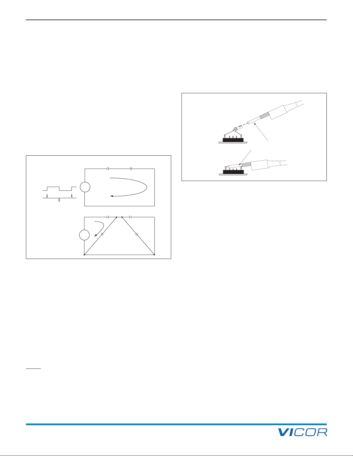
C
FET
C
Rectifier
I
CM
C
FET
C
Rectifier
C
External
C
External
I
CM
Primary Secondary
V
p
V
p
V
p
Baseplate
I
DM
Y
caps Ycaps
9. EMC Considerations
To Scope
Ground Ring on Probe
T
o Scope
or
I
nsert probe into female receptacle
(Vicor P/N 06207) for proper output
d
ifferential noise measurement technique
or VI-200 and VI-J00 Family DC-DC Converters and Configurable Power Supplies
F
Design Guide & Applications Manual
The dv/dt of the switch (FET) is a noise generator. This
FET is mounted on a two layer insulating and shielding
assembly which is attached to the baseplate. Since ceramic
s a dielectric, there is capacitance from the FET to the
i
baseplate. (Figure 9–7) The output rectifiers are also tied
o the baseplate with ceramic insulators, adding additional
t
capacitance. The dv/dt of the FET is differentiated by these
two series capacitors, resulting in a spike of noise current
at 50 – 70 MHz that flows from primary to secondary.
(Figure 9–8) This noise current is common-mode as opposed
to differential, and therefore should not affect the operation
of the system. It should be noted, however, that oscilloscopes
have a finite ability to reject common-mode signals, and
these signals can be abnormally emphasized by the use of
long ground leads on the scope probe.
have very short leads since the frequency is high. It must
also be a good capacitor (i.e., ceramic or other material
that has a low ESR / ESL). This type of capacitor is most
mportant on high input voltage units since the “dv”
i
is larger, but is required for all units. For off-line
pplications this capacitor must have the appropriate
a
safety agency approvals.
Figure 9–9 — Output ripple measurement technique
A capacitor from +/–Vout to the baseplate, is required
since the output rectifier has a changing voltage on it,
and, like the FET, can generate common-mode noise.
This capacitor is similarly recommended for high output
voltage units (48 V).
Figure 9–8 — Noise coupling model
MEASURING OUTPUT NOISE
Long ground leads adversely impact the common-mode
rejection capability of oscilloscopes because the ground
lead has inductance not present on the signal lead. These
differing impedances take common-mode signals and
convert them to differential signals that show up on the
trace. To check for common-mode noise, place the
oscilloscope probe on the ground lead connection of the
probe while the ground lead is tied to output return.
(Figure 9–9) If the noise is common-mode, there will still
be “noise” observed at the same test point.
: The output return must be at the same relative
NOTE
potential as the earth ground of the oscilloscope or
ground lead.
Capacitors are required from the +/–IN to the baseplate
damaging current may flow through the oscilloscope
thereby shunting common-mode current, thus reducing
noise current on the input power lines. The capacitor must
Common-mode noise is not differential with respect to
the output. It does, however, flow in both input and
output leads of the power supply and is a noise parameter
that is measured by the FCC or VDE. It can cause power
systems to fail radiated emission tests, so it must be dealt
with. Bypass capacitors to the baseplate with a commonmode filter on the input of the module or the main input
of the power supply is required.
The common-mode filter is typically placed on the input as
opposed to the output. Theoretically, since this current
flows from primary to secondary, the choke could be
placed in either the input or the output, but is preferably
placed in the input leads for the following reasons:
1) input currents are smaller since the input voltage is
usually higher;
2) line regulation of the module can correct for voltage
drops across the choke; and
3) if the choke is on the output and the senses are
connected to the other side of it, the stability of the
loop may be impacted.
Differential output noise is the AC component of the
output voltage that is not common to both outputs. The
noise is comprised of both low frequency, line-related
noise (typically 120 Hz) and high frequency switching noise.
VI-200 and VI-J00 Family Design Guide Rev 3.5 vicorpower.com
Page 24 of 98
Apps. Eng. 800 927.9474 800 735.6200
Page 26
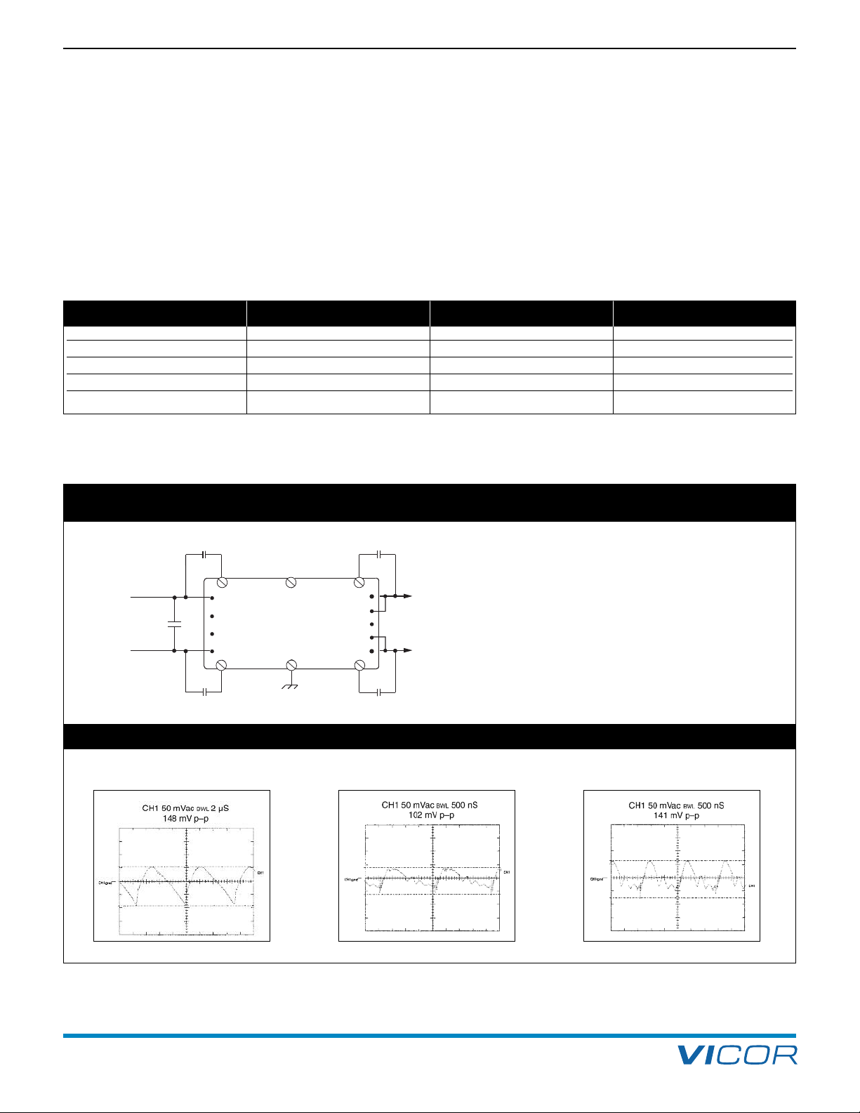
Design Guide & Applications Manual
+IN
–IN
+OUT
–OUT
C2
a
C1
C3
a
C2
b
C3
b
GATE
OUT
GATE
IN
+S
TRIM
–S
C1 = 100 µF
C2a – C2b = 4,700 pF (Vicor Part # 01000)
C3a – C3b = 0.01 µF (Vicor Part # 04872)
Conditions
Light Load = 3 A
Nominal Load = 15 A
Full Load = 30 A
or VI-200 and VI-J00 Family DC-DC Converters and Configurable Power Supplies
F
9. EMC Considerations
High Frequency Switching Noise. Peak-to-peak output
voltage ripple is typically 2% or less (1% for 12 V outputs
and above). Hence additional output filtering is generally
ot required. Digital systems rarely need additional
n
filtering. However some analog systems, such as
ltrasound systems, will probably require additional output
u
filtering. See additional output filter choices in Table 9–1.
Line Related Output Noise. Line related output noise
can be determined from the converter specification —
Input Ripple Rejection. As an example, a VI-260-CV
(300 Vin to 5 Vout) has a rejection specification at 120 Hz
of 30 + 20 Log (Vin / Vout). Vin = 300 and Vout = 5,
hence its rejection is 30 + 35.56 = 65.56 dB, which
rovides an attenuation factor of 1.89 k. Therefore, if the
p
input to the converter has 30 V p-p of ripple, the output
-p ripple would be 15.8 mV. It is not practical to
p
attenuate this component further with passive filtering
due to its low frequency, hence active filtering is required.
The RAM contains both a passive filter for high frequency
noise and an active filter for low frequency noise.
5 V Outputs 12 – 15 V Outputs 24 – 48 V Outputs
No Additional Filter 2% p-p (Typical) 1% p-p (Typical) 0.2% p-p (Typical)
Low ESR Output Cap. 1% p-p (Typical) 0.5% p-p (Typical) 0.1% p-p (Typical)
LC Output Filter 0.4% p-p (Typical) 0.2% p-p (Typical) 0.05% p-p (Typical)
RAM Filter (VI-200) <3 mV p-p (Maximum) <3 mV p-p (Maximum) <3 mV p-p (Maximum)
RAM Filter (VI-J00) <10 mV (Maximum) <10 mV (Maximum) <10 mV (Maximum)
Table 9–1 — Output filter options and output voltage and ripple
Differential Output Filtering
Typical Vicor Module (VI-230-CV) 48 V Input, 5 V Output
Output Ripple vs. Load
3 Amp Load 15 Amp Load 30 Amp Load
Figure 9–10 — Output noise, no additional output filtering
VI-200 and VI-J00 Family Design Guide Rev 3.5 vicorpower.com
Page 25 of 98
Apps. Eng. 800 927.9474 800 735.6200
Page 27
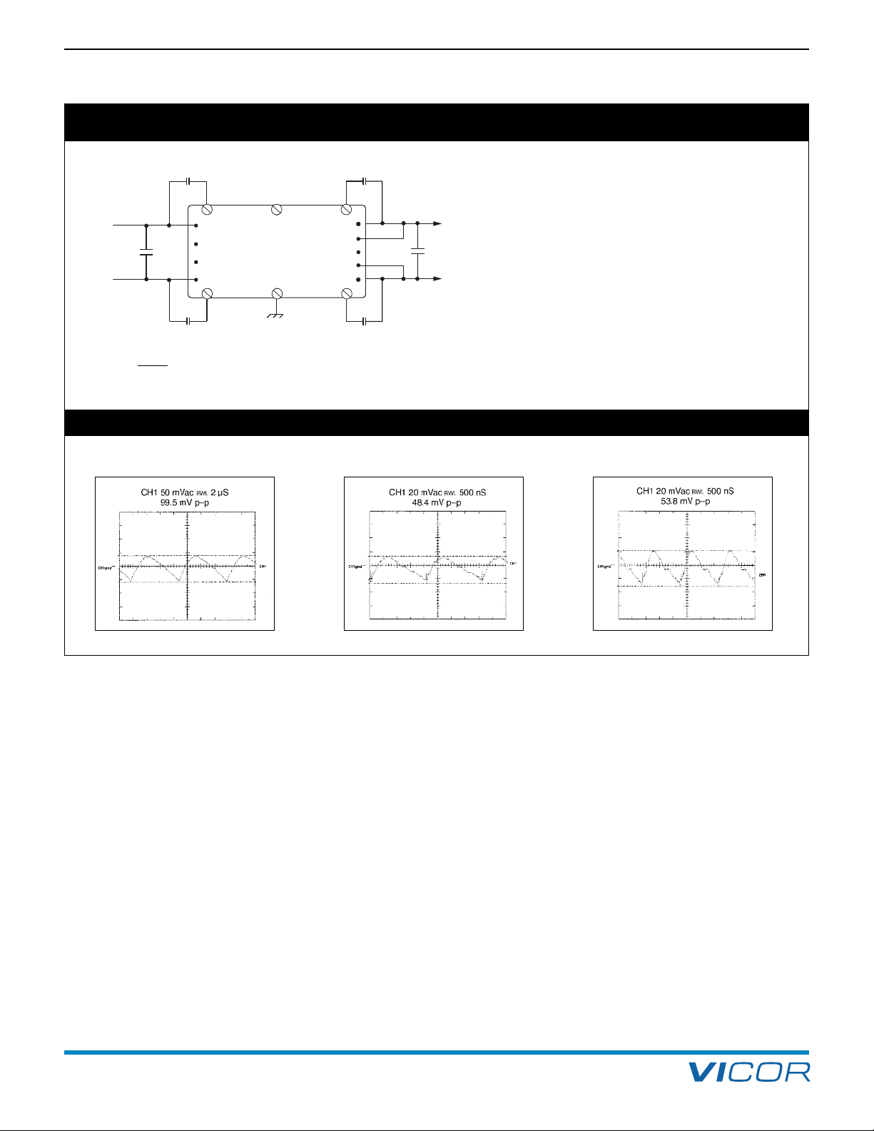
9. EMC Considerations
+
IN
–
IN
+OUT
–OUT
C3
a
G
AT E
IN
GAT E
OUT
+
S
TRIM
–
S
C4
C
2
a
C1
C
2
b
C3
b
C1 = 100 µF
C 2a – C2b = 4,700 pF (Vicor Part # 01000)
C 3
a
– C3
b
=
0.01 µF (Vicor Part # 04872)
C4 = 270 µF (Tant.)
Conditions
Light Load = 3 A
Nominal Load = 15 A
Full Load = 30 A
NOTE: A low ESR capacitor should be used on the output, preferably tantalum.
or VI-200 and VI-J00 Family DC-DC Converters and Configurable Power Supplies
F
Addition of Output Capacitor
Typical Vicor Module (VI-230-CV) 48 V Input, 5 V Output
Output Ripple vs. Load
Design Guide & Applications Manual
3 Amp Load 15 Amp Load 30 Amp Load
Figure 9–11 — Output noise, additional output capacitance
Apps. Eng. 800 927.9474 800 735.6200
VI-200 and VI-J00 Family Design Guide Rev 3.5 vicorpower.com
Page 26 of 98
Page 28
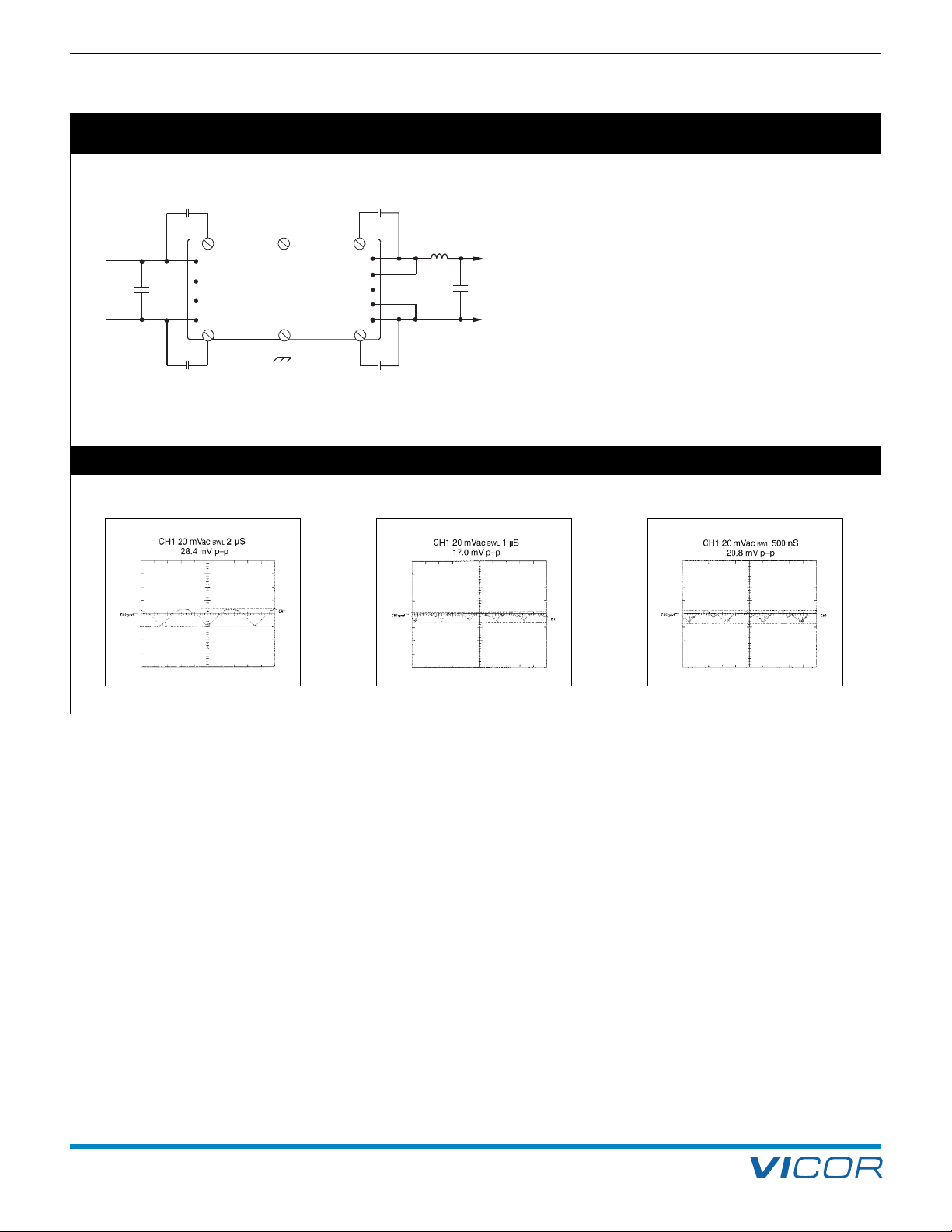
Design Guide & Applications Manual
C1 = 100 µF
C2a – C2b = 4,700 pF (Vicor Part # 01000)
C3a – C3b = 0.01 µF (Vicor Part # 04872)
C4 = 270 µF (Ta n t .)
L1 = 200 nH (Vicor Part # 30268)
Conditions
Light Load = 3 A
Nominal Load = 15 A
Full Load = 30 A
+
IN
–
IN
+OUT
–OUT
C3
a
GATE
I
N
GATE
OUT
+
S
T
RIM
–S
C2
a
C1
C
2
b
C3
b
C
4
L
1
or VI-200 and VI-J00 Family DC-DC Converters and Configurable Power Supplies
F
Typical Vicor Module (VI-230-CV) 48 V Input, 5 V Output
9. EMC Considerations
LC Output Filter
Output Ripple vs. Load
3 Amp Load 15 Amp Load 30 Amp Load
Figure 9 –12 — Output noise, additional output inductor and capacitor (L-C Filter)
VI-200 and VI-J00 Family Design Guide Rev 3.5 vicorpower.com
Page 27 of 98
Apps. Eng. 800 927.9474 800 735.6200
Page 29
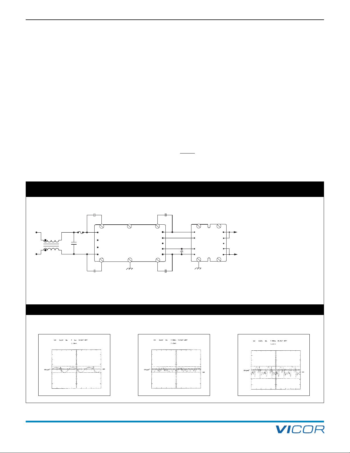
9. EMC Considerations
C1 = 100 µF
C2a – C2b = 4,700 pF (Vicor Part # 01000)
C3a – C3b = 0.01 µF (Vicor Part # 33643)
C4 = 220 µF (Electrolytic)
Conditions
Light Load = 3 A
Full Load = 15 A
Overload Condition = 30 A
+IN
–IN
+OUT
–OUT
C3
a
C3
b
GATE
IN
GATE
OUT
+S
TRIM
–S
C2
a
C2
b
C1
+IN
–IN
–OUT
–S IN
+S IN
+OUT
RAM
+S
–S
+
–
L1
C4
+
CM
RAM / MI-RAM OPERATION
or VI-200 and VI-J00 Family DC-DC Converters and Configurable Power Supplies
F
Design Guide & Applications Manual
The RAM / MI-RAM attenuates output noise in two ways.
First, an LC filter in the RAM/ MI-RAM attenuates high
frequency components associated with the switching
frequency. Secondly, the RAM/ MI-RAM contains an active
filter that attenuates low frequency components associated
with the input to the converter. These frequencies are on
the order of 60 – 120 Hz and harmonics would require
very large output LC if a passive approach were to be
used. Essentially, the active circuit looks at the output
ripple from the converter, multiplies it by –1 (inverts) and
adds it to the output. This effectively cancels out the low
frequency components.
The RAM does not contain any common-mode filtering,
so whatever common-mode noise is present is passed
through. It only provides differential filtering of noise that
is present on one output pin relative to the other.
RAM Output Filter
Typical Vicor Module (VI-230-CV) 48 V Input, 5 V Output with VI-RAM-C2
The use of the RAM / MI-RAM is very straightforward, but
a couple of precautions should be noted. The LC filter is in
the positive output lead, so if that lead is shorted then the
high frequency attenuation is compromised. The active
circuit is in the negative output lead, so if that lead is
shorted the low frequency attenuation is compromised.
The RAM must be used with a common-mode choke at
the input of the converter.
The RAM is intended to be used with the Vicor VI-200 /
VI-J00, and the MI-RAM is intended to be used with Vicor
MI-200/ MI-J00 Family of DC-DC converter modules. It is
also available in a chassis mounted version as VI-LRAM-xx
(MegaMod package) or VI-RAM-xx-B1 (BusMod package).
NOTE: Do not use if load is inductive as instability
may result. The addition of the RAM will increase the
converter’s current limit setpoint by ~ 14%.
Output Ripple vs. Load
3 Amp Load 15 Amp Load
Figure 9–13 — Output noise, with Ripple Attenuator Module (RAM)
VI-200 and VI-J00 Family Design Guide Rev 3.5 vicorpower.com
Page 28 of 98
Apps. Eng. 800 927.9474 800 735.6200
30 Amp Load
(Overload Condition)
Page 30
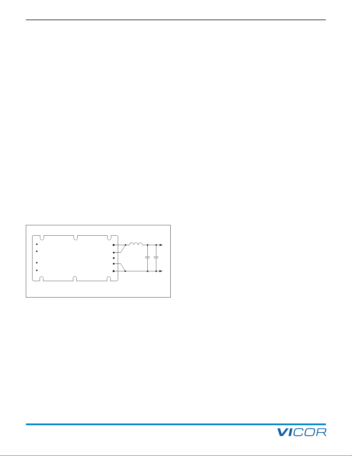
Design Guide & Applications Manual
–OUT
–S
+S
+
OUT
+
IN
GATE
I
N
GATE
OUT
–IN
TRIM
L1
C1
C2
or VI-200 and VI-J00 Family DC-DC Converters and Configurable Power Supplies
F
10. Optional Output Filters
OVERVIEW
The LC filter design below is a comparatively simple solution
for reducing ripple on the outputs of Vicor’s VI-200 and
VI-J00 Family converter modules. These components are
mall and provide significant peak-to-peak noise attenuation.
s
Since an output filter capacitor is already present in the
DC-DC converter, adding an inductor and capacitor to the
output creates a pi filter. It is important that the inductor
wire be of a size sufficient to carry the load current,
including a safety factor, and that the core does not
saturate. LC filters are generally needed only where very
accurate analog signals are involved.
The RAM/MI-RAM (Ripple Attenuator Module) should be
used if greater attenuation of output ripple is required, or
where additional AC power line ripple frequency rejection
is required.
All standard outputs will function with either remote sense
or local sense, with the recommended capacitance. Lower
ESR is achieved with capacitors in parallel. Ripple data
measured at 20 MHz bandwidth limit.
Adding excessive amounts of external filtering may
compromise the stability of the converter and result in
oscillation.
FILTER COMPONENTS FOR 5 V OUTPUT
• L1 — Vicor P/N 30268 or Micrometals #T38-26/90 core
with 2T #14 wire (200 nH)
C1, C2 — Vicor P/N 30800, 270 µF / 10 V,
•
solid tantalum, ESR 90 m
Ω typical
• Typical data at high line input:
With full load, ripple ~ 11 mV p-p
With 50% load, ripple ~ 8 mV p-p
FILTER COMPONENTS FOR 12 V AND 15 V OUTPUTS
• L1 — Vicor P/N 30268 or Micrometals #T38-26/90 core
with 2T #14 wire (200 nH)
• C1, C2 — Vicor P/N 30506, 120 µF / 20 V,
solid tantalum, ESR 90 mΩ typical
• Typical data at high line input:
With full load, ripple ~ 5 mV p-p
With 10% load, ripple ~ 15 mV p-p
FILTER COMPONENTS FOR 24 V AND 28 V OUTPUTS
• L1 — Vicor P/N 30268 or Micrometals #T38-26/90 core
with 2T #14 wire (200 nH)
Figure 10 –1 — Recommended LC output filter
• C1, C2 — Vicor P/N 30507, 68 µF / 30 V,
solid tantalum, ESR 160 mΩ typical
• Typical data at high line input:
With full load, ripple ~ 6 mV p-p
With 10% load, ripple ~ 18 mV p-p
VI-200 and VI-J00 Family Design Guide Rev 3.5 vicorpower.com
Page 29 of 98
Apps. Eng. 800 927.9474 800 735.6200
Page 31

DC Input
BatMod
GATE
IN
GATE
OUT
+OUT
–OUT
+IN
–IN
External
C
ontrol
Functions
+
–
L
oad
TRIM
V
TRIM
I
MON
I
DC Input
BatMod
GATE
IN
GATE
OUT
+OUT
–OUT
V
I
MON
+IN
–IN
External
Control
Functions
GATE
IN
GATE
OUT
+OUT
–OUT
+IN
–IN
BatMod
Booster
GATE
IN
GATE
OUT
+OUT
–OUT
+IN
–IN
Enable/
Disable
+
–
Load
TRIM
TRIM
I
BatMod
Booster
11. Battery Charger (BatMod)
OVERVIEW
or VI-200 and VI-J00 Family DC-DC Converters and Configurable Power Supplies
Design Guide & Applications Manual
F
The BatMod is a programmable current source module
that is intended for battery charging or simular current
source applications. It can be controlled externally to meet
a wide range of charging parameters: voltage, current,
charge rate and charge time.
The BatMod is comparable to the VI-200 voltage source
module but with a variable current limit. It has three
output pins that differ from the VI-200 converters:
Current Control (IT
RIM
), Voltage Adjust (VT
RIM
) and Current
Monitor (IMON). All of these pins are referenced to the
–OUT pin.
Although the BatMod is primarily intended for battery
charge applications it can be used as a programmable
current source for resistive loads or CW laser diodes. The
BatMod will not function properly at zero output voltage
and current simultaneously. It follows therefore that the
current can not be adjusted to zero with a resistive load.
Refer to Safe Operating Area Curves on the BatMod data
sheet, which can be found at vicorpower.com.
PINOUT DESCRIPTION
Current Control (ITRIM). An input which can receive an
analog control voltage from 1 – 5 V for adjustment of the
sourced current from zero to maximum rating of the BatMod.
5 Vdc 100% of Rating
=
1 Vdc 0 Amps
ON
M
Current Monitor (I
). An output that indicates the
amount of current being sourced. It is a linear voltage /
current relationship where one volt corresponds to 0%
of sourced current and 5 V corresponds to 100% of
sourced current.
5 Vdc 100% of Rating
=
1 Vdc 0 Amps
For DC input / current source applications (Figure 11–1),
the BatMod has a similar wide range input rating as the
VI-200 Family of voltage converters for 48 and 300 V
inputs. BatMods can be used for higher current source
applications with a Driver / Booster approach. (Figure 11–2)
NOTE: Inductance to the load should be limited to
20 µH to avoid possible loop instabilities.
Figure 11–1 — DC input single module
Voltage Adjust (VTRIM). An input for controlling or
setting the output setpoint, this is similar to the trim
function on the VI-200. (Section 5) A maximum voltage
can be set by a fixed resistor or adjusted with an external
voltage source. A source voltage referenced to –OUT
adjusted from 1.25 – 2.5 V will program a 50 – 100% of
rated voltage setting.
2.5 Vdc Max. V
out
=
1.25 Vdc 50% of V
It is important to note the nominal output voltage for
each BatMod type untrimmed.
out
12 Vout Part # = 15 V actual
24 Vout Part # = 30 V actual
VI-200 and VI-J00 Family Design Guide Rev 3.5 vicorpower.com
Page 30 of 98
48 Vout Part # = 60 V actual
Apps. Eng. 800 927.9474 800 735.6200
Figure 11–2 — DC input high power array
Page 32

Design Guide & Applications Manual
or VI-200 and VI-J00 Family DC-DC Converters and Configurable Power Supplies
F
DESIGNING A BATTERY CHARGER
11. Battery Charger (BatMod)
Vicor’s BatMod (current source module) enables designers
to easily build a compact, lightweight battery charging
system with commonly available parts. The BatMod
provides programmable output current and output voltage
capability. Since the BatMod allows the output voltage
and the charge current to be set independently, the
system design is greatly simplified.
Basic Battery Charger. Figure 11–3, shows a basic
charging circuit with a BatMod for the following
system requirements:
Battery voltage: 12 V
Float voltage: 13.8 V
Charge current: Adjustable 0 – 14.5 A
Setting the Float Voltage. Since the open circuit output
of a 12 V BatMod (VI-2x1-CU-BM) is 15 V, a trim resistor
(R3) is necessary to set the float voltage of 13.8 V.
Steps to determine the value of R3:
Solve for VTRIM:
Solve for VR5:
VFLOAT
VNOM
(
13.8 V
(
VREF – VTRIM = VR5
2.5 V – 2.3 V = 0.2 V
15 V
VREF =VTRIM
)
2.5 V = 2.3 V
)
Setting the Charge Current. The charge current can
be programmed from 0 to maximum (14.5 A) by applying
1 – 5 V to the I
to produce a particular charge current, 10 A for example,
use the following formula:
4
4
To set the input voltage at IT
potentiometer (R2) appropriately.
In Figure 11–3 the configuration will charge the battery
at a maximum of 10 A with a 13.8 V float voltage. Other
charge rates and float voltages may be similarly calculated.
If a fixed charge current is desired, the potentiometer can
be replaced with two fixed resistors. In applications requiring
tight control over the charging current, D1 can be replaced
with a precision reference.
Advanced Battery Charger. Many new battery technologies
require sophisticated charging and monitoring systems to
preserve their high performance and to extend their life.
The Bat Mod serves as an ideal building block for
constructing an advanced battery management system,
which typically incorporates a microprocessor-based
control circuit that is easily adapted for a variety of battery
chemis tries and monitoring functions. (Figure 11–4)
TRIM pin. To determine the voltage required
Desired Charge Current
Maximum Output Current
(
10 A
14.5 A
(
+1=3.76 V
)
RIM
+1=IT
)
to 3.76 V, adjust the
RIM
voltage
Solve for IR5:
VR5=0.2 V
IR5 =
R5 10 kΩ
Solve for R3:
VTRIM
= R3
IR5
2.3 V
20 µA
A 13.8 V output requires a 115 kΩ resistor.
VI-200 and VI-J00 Family Design Guide Rev 3.5 vicorpower.com
Page 31 of 98
= 115 kΩ
= 20 µA
Apps. Eng. 800 927.9474 800 735.6200
To maintain the optimum charge on the battery, the
control circuit independently adjusts the float voltage and
charge current in response to conditions during the
charge: the battery’s voltage, current, temperature and
pressure, and other pertinent parameters. It can also relay
battery status information such as capacity, charge and
discharge history, and cause of failure.
NOTE: A redundant control or monitoring circuit
must be included if failure of the BatMod or its
control circuit will result in uncontrolled charging of
the battery. Many new battery types are sensitive to
these conditions and may result in fire or explosion.
With its wide range of outputs, the BatMod offers
designers a simple, cost-effective solution to battery
charging for all major battery types.
Page 33

V
TRIM
I
TRIM
I
M
ON
+OUT
–OUT
To Front End:
AIM,
H
AM,
IAM, or
Off-Line
Front End
+
IN
–
IN
GATE
I
N
G
ATE
OUT
BatMod VI-2x1-CU-BM
Error
A
mp
R5
10 kΩ
REF
2.5 V
R
ITRIM
≈ 50 kΩ
10 mA
R
1
820 Ω
D1
5
.1 V
Zener
1 mA
R
2
5 kΩ
R3
115 kΩ
1
2 V
V
T
RIM
I
T
RIM
I
MON
Control Circuitry
• Voltage
• Battery Temp.
• Ambient Temp.
• Other
+OUT
–OUT
System
Status
11. Battery Charger (BatMod)
Figure 11–3 — Basic charging circuit using a current source module (BatMod)
or VI-200 and VI-J00 Family DC-DC Converters and Configurable Power Supplies
Design Guide & Applications Manual
F
Figure 11–4 — The BatMod in an advanced battery charging system
VI-200 and VI-J00 Family Design Guide Rev 3.5 vicorpower.com
Page 32 of 98
Apps. Eng. 800 927.9474 800 735.6200
Page 34

Design Guide & Applications Manual
EMI
Filter
10 V
U2
U1
OC
O
V
V
ref
2
V
ref 1
+
OUT
–
OUT
G
ATE IN
GATE OUT
PARALLEL
Q
1
Q
2
Level
Shift
D2
D
1
C2
L1
L2/N
L1
L2/N
+IN
–IN
+OUT
–OUT
+OUT
–OUT
VI-AIM
DC-DC CONVERTER
C1
[a]
AC IN
LOAD
P
IM
P
OM
0.47 µF
[a]
C1 is a hold-up capacitor necessary for proper operation of the AIM.
Hold-up capacitors are available at vicorpower.com.
or VI-200 and VI-J00 Family DC-DC Converters and Configurable Power Supplies
F
OVERVIEW
12. AC Input Module (AIM/MI-AIM)
In combination with VI-200 and VI-J00 Family of DC-DC
converter modules, the Alternating Input Module (AIM)
provides a high density, low profile, universal AC input
off-line switching power supply for systems requiring
up to 200 W of total output power. The AIM accepts
85 – 264 Vac, with a DC output voltage proportional to
the peak value of the AC line. The input voltage required
for the AIM to start operating is between 82 V and 90 Vrms
(non-distorted sinusoid).
The DC output of the AIM is the peak rectified line
(Vac RMS X 2 ), thus, 85 Vac corresponds to 120 Vdc
√
and 264 Vac corresponds to 373 Vdc. Since the DC
output range is wide, a “7” (100 – 375 V) designator for
input voltage in the part number of the DC-DC converter
is required. However, the “5” (100 – 200 V) designator
for the DC-DC converter part number is available for
domestic AC inputs only and the “6” (200 – 400 V)
designator for European AC inputs only, potentially
reducing the number of modules required in some
applications, based on output power capability.
SUMMARY OF COMPATIBLE DOWNSTREAM
DC-DC CONVERTERS
Input overvoltage conditions cause the GATE IN pin of the
AIM to disable the converters when the output bus voltage
is in the range of 406 – 423 Vdc. Input undervoltage
conditions cause the GATE IN to disable the converters
when the output bus voltage drops within the range of
68 – 89 Vdc.
CAUTION
: The AIM is not isolated. Do not place scope
probes on input and output of AIM simultaneously. Do
not connect the output of the AIM to earth ground.
The GATE OUT of the AIM must be connected to the
GATE OUT of only one DC-DC converter. This input signal
to the AIM controls a charge pump (D1, D2, C2) that
biases the gate of Q1, 10 V above its source, which turns
on Q1 to shunt out a PTC thermistor that limits inrush.
Multiple DC-DC converters operating from an AIM may
make it difficult to guarantee a 10% load on the DC-DC
converter that provides the GATE OUT signal to the AIM.
In this instance, other DC-DC converters can charge pump
the FET through the PARALLEL pin, with the addition of
two diodes and a capacitor to each Driver module.
(Figure 12–4)
Use VI-x7x for inputs of 85–264 Vac; VI-x6x for inputs of
170–264 Vac; or VI-x5x for inputs of 85–135 Vac. EMC
filtering specifications of FCC Level A are met by adding
a 0.47 µF “X-type” capacitor to the input of the AIM
(Vicor Part #03047); “Y-type” bypass capacitors must also
be added from the +/– inputs of the DC-DC converters to
their respective baseplates, which are grounded (Vicor
Part #01000, 4,700 pF). To select the hold-up capacitor
appropriate for your application, (refer to Selecting
Capacitors for AIM Modules section that follows).
The output ripple of the AIM is a function of output load.
It is necessary to keep the ripple less than 20 V p-p to
ensure the under / overvoltage protection circuits will not
trigger. A fully loaded AIM (200 W of module output
power) requires a minimum of 680 µF of capacitance;
hold-up requirements can be met with this capacitor and
maximum total capacitance should not exceed 1,200 µF
(refer to Selecting Capacitors for AIM Modules section
that follows). The voltage rating of this capacitor will be
determined by the input operating voltage.
It is necessary to connect all “Driver” DC-DC converter
GATE IN pins to the GATE IN pin of the AIM . This GATE IN
to GATE IN connection is used to disable the converters at
turn-on to allow proper start-up of the AIM. The DC-DC
converters are then enabled through the GATE IN pin when
the output bus voltage is in the range of 113 – 123 Vdc.
VI-200 and VI-J00 Family Design Guide Rev 3.5 vicorpower.com
Page 33 of 98
Figure 12–1 — Block diagram, AIM /MI-AIM
Figure 12–2 — System block diagram (supervisory connections
Apps. Eng. 800 927.9474 800 735.6200
not shown)
Page 35

RECTIFIED
A
C
T0 T1 T2 T3 T4
Vp
V
v
Vdo
TIME
T
5
12. AC Input Module (AIM/MI-AIM)
SELECTING CAPACITORS FOR AIM MODULES
or VI-200 and VI-J00 Family DC-DC Converters and Configurable Power Supplies
F
Design Guide & Applications Manual
Hold-up Time. For maximum flexibility, an external
capacitor (Figure 12–2, C1) is used to set the system’s
hold-up requirements. Hold-up time, for purposes of this
application note, is defined as the time interval from loss
of AC power to the time a DC-DC converter begins to
drop out of regulation (Figure 12–3, T4 to T5). Hold-up
time is a function of line voltage, hold-up capacitance,
output load, and that point on the AC waveform where
the line drops out. For example, if the AC line fails just
after the hold-up capacitors were recharged, hold-up time
will be much greater (Figure 12–3, T3 to T5) than if the
AC line fails just prior to another recharge (Figure 12–3,
T4 to T5).
The basic equations involved in calculating hold-up time are:
1
XC1X
22
Vp2–
1
C1XVd
X
2
o
M
=PI
(T5 – T3) (1)
X
solving for C1:
C1 = 2 X
PIMx (T5 – T3)
2
Vp2 – Vd
o
(2)
Where PIM is power delivered from the AIM:
Module Output Power
PIM=
=
PO
M
(3)
Module Efficiency Eff. % / 100
The energy (Joules) delivered from the AIM from the time
power is lost (T4), until loss of an output (Figure 12–2, T5):
Energy (Joules) = PIM x (T5 - T4) (Watt – Seconds) (4)
Figure 12–3 — AC waveforms
where: POM = Output power from all the modules
PIM = Input power to the modules
(output power from the AIM)
Eff = Weighted average efficiency of all modules
The input power to the converter(s) during normal operation
is supplied from the AC line during the conduction time
of the rectifiers (T2 to T3) internal to the AIM and by the
energy stored in C1 when the rectifiers in the AIM are
reverse biased (T1 to T2). In the event of an AC failure
(T4), C1 must continue to provide energy to the converters
until either AC returns or the converter drops out (T5).
The energy stored in C1 at the peak of the AC is:
1
C1xVp2=Joules (5)
x
2
The energy stored in C1 when the converter drops out of
regulation is:
1
x
C1xVdo2= Joules (6)
2
The energy delivered by C1 to the converters during
normal operation is:
PIMx(T2 – T1) = Joules (7)
VI-200 and VI-J00 Family Design Guide Rev 3.5 vicorpower.com
Page 34 of 98
Apps. Eng. 800 927.9474 800 735.6200
Page 36

Design Guide & Applications Manual
or VI-200 and VI-J00 Family DC-DC Converters and Configurable Power Supplies
F
12. AC Input Module (AIM/MI-AIM)
CHOOSING APPROPRIATE VALUES FOR AIM MODULES
Sample calculation:
Converter output power (POM) = 100 W
ine frequency = 60 Hz
L
Line range = 105 – 264 Vac
Efficiency = 82%
Desired hold-up time = 5 ms (minimum)
therefore:
PIM=
100
= 122 W
0.82
T5 – T3 = 5 ms + 8.3 ms = 13.3 ms
(minimum hold-up time plus half cycle)
Vp = 105 X 2 = 148 V
√
Vdo = 100 V
and:
2 X 122 X 0.0133
C1 =
1482– 100
2
C1 = 270 µF
where:
VP = The peak of the rectified AC line or 2 X Vacin.
√
For an input range of 85 – 264 Vac, this voltage
will vary from 120 – 373 V.
VV = The low point of the rectified AC line under
normal operating conditions. This “valley” voltage
is a function of C1, PIM and line frequency. The
peak-to-peak ripple across C1 is VP – VV and
determines the ripple current in C1.
NOTE: It is important to verify the rms ripple
current in C1 with a current probe.
do = Voltage at which the DC-DC converter(s) begin(s) to
V
drop out of regulation. This voltage is from the data
sheet of the appropriate module, which for the
VI-270 Family is 100 Vdc. Under normal operating
conditions, VV must exceed Vdo.
T1 = The peak of the rectified AC line or the point at
which C1 is fully charged. For an input range of
85 – 264 Vac, this voltage will vary from 120 – 373 V.
T2 = The low point of the rectified AC line under
normal operating conditions and the point at
which C1 is about to be “recharged”. This is the
point of lowest energy in C1.
T4 = The low point of the rectified AC line; the point
of lowest energy in C1; the point at which if the
AC line fails, hold-up time is shortest, i.e., “worst
ase”.
c
T5 = The time at which the converter(s) drop out of
regulation.
T5 – T4 = Minimum hold-up time. Actual hold-up time
may vary up to a maximum of T5 – T3.
(T3 – T1) X 2 = One line cycle.
The following values are calculated in a similar manner.
Module(s) 60 Hz 50 Hz
Delivered Power 90 Vac 105 Vac 90 Vac 105 Vac
50 W 270 µF 135 µF 300 µF 150 µF
75 W 400 µF 200 µF 440 µF 230 µF
100 W 525 µF 270 µF 600 µF 300 µF
150 W 800 µF 400 µF 890 µF 455 µF
200 W 1,000 µF 540 µF 1,180 µF 600 µF
Table 12–1 — Hold-up capacitor values for use with VI-270 /VI-J70
and the VI-250 / VI-J50 DC-DC converters.
C1 values as a function of line voltage, frequency and
delivered power, for use with the “7” input designator
DC-DC converters (AIM input of 90–264 Vac) or “5” input
designator (AIM input of 90–132 Vac) DC-DC converters.
NOTE
: With “7” input DC-DC converters operated
from the AIM input range of 90 – 264 Vac, 400 V
capacitors must be used (Vicor Part #30240). With
“5” input DC-DC converters used over the AIM input
range of 90 – 132 Vac, 200 V capacitors may be used
(Vicor Part #30769).
Module(s) 60 Hz 50 Hz
Delivered Power 180 Vac 210 Vac 180 Vac 210 Vac
50 W 66 µF 34 µF 74 µF 38 µF
75 W 100 µF 50 µF 110 µF 60 µF
100 W 130 µF 67 µF 150 µF 75 µF
150 W 200 µF 100 µF 220 µF 115 µF
200 W 262 µF 135 µF 300 µF 150 µF
Table 12–1 — Hold-up capacitor values for use with VI-260 /VI-J60
DC-DC converters.
C1 values as a function of line voltage, frequency and
delivered power, for use with the “6” input designator
DC-DC converters (AIM input of 180 – 264 Vac).
NOTE: With “6” input DC-DC converters operated
from the AIM input range of 180 – 264 Vac,
400 V capacitors must be used (Vicor Part #30240).
VI-200 and VI-J00 Family Design Guide Rev 3.5 vicorpower.com
Page 35 of 98
Apps. Eng. 800 927.9474 800 735.6200
Page 37

D1
D2
D2
C2
C2
–
OUT
–S
TRIM
+S
+OUT
+
IN
GAT E
IN
GAT E
OUT
–IN
–OUT
–
S
TRIM
+S
+OUT
+
IN
GATE
IN
GATE
OUT
–
IN
–OUT
–S
TRIM
+S
+OUT
+IN
GATE
I
N
GATE
OUT
–
IN
AIM
G
ATE OUT
PA R
G
ATE IN
+OUT
–OUT
L2/N
NC
N
C
L1
D1, D2: 1N4148
C2: 470 pf / 500 V
D3: 1N4006
D1
Universal
AC In
Bussman Fuses,
PC Tron
0.47 µF
C1
[a]
Driver
Driver
D
river
[
a]
Refer to Selecting Capacitors for
AIM Modules in the begining of this
Section. Refer to Typical application
for Vic or co nverter with AIM,
Figure 12–5, for recommended
external components.
D3
D3
D3
Y-capacitors not shown for clarity
Universal
AC In
AIM
GATE OUT
PA R
GATE IN
+OUT
–OUT
L2/N
NC
NC
L1
0.47 µF
–OUT
–S
TRIM
+S
+OUT
+IN
GATE
IN
GATE
OUT
–IN
VI-200/J00
Driver
Load
F2
0.01 µF (Two 4,700 pF)
Y-Rated Capacitors
0.01 µF (Two 4,700 pF)
Y-Rated Capacitors
0.01 µF Ceramic
0.01 µF Ceramic
C1
[a]
F1
[a]
Consult factory or refer to Selecting Capacitors for AIM Modules at the begining of this section.
Z1: MOV Part #30076
Fuse 1: 6.3A/250V (IEC 5X20 mm) Buss GDB-6.3 or 7 A / 250 V (3AG 1/4" x 1 1/4") Littlefuse 314-007
Fuse 2: For VI-X7X-XX — Buss PC-Tron 2.5 A (250 V)
For VI-X6X-XX — Buss PC-Tron 3 A (250 V)
For VI-X5X-XX — Buss PC-Tron 5 A
Z1
12. AC Input Module (AIM/MI-AIM)
Figure 12–4 — AIM connection diagram, multiple Driver DC-DC converters
or VI-200 and VI-J00 Family DC-DC Converters and Configurable Power Supplies
Design Guide & Applications Manual
F
Figure 12–5 — Typical application for Vicor converter with AIM
VI-200 and VI-J00 Family Design Guide Rev 3.5 vicorpower.com
Page 36 of 98
Apps. Eng. 800 927.9474 800 735.6200
Page 38

Design Guide & Applications Manual
Note:
Non-Isolated
Output
Gate In
Gate Out
ZCS
Boost
Converter
Inrush
& Short
Circuit
Protection
High Frequency
Control
Voltage
Waveform
Current
Sense
AC
Line
Control
& House-
keeping
Circuitry
Output Voltage
Module Enable
Power OK
DC
Out
Recti-
fier
Aux. Supply
+
–
NOTE: No input to output isolation.
Input Voltage
V
RMS
Rated Output Power
O
utput Voltage
Output Power (W)
Output Voltage (Vdc)
3
50
400
450
500
550
600
650
85
190
260
330
4
00
3
65
435
295
225
95
105
115
125
135
1
45
155
165
1
75
185
1
95
205
215
225
235
2
45
255
265
110 Vac
700
d
e
r
a
t
e
o
u
t
p
u
t
p
o
w
e
r
8
W
/
V
f
o
r
V
in
<1
1
0
V
a
c
or VI-200 and VI-J00 Family DC-DC Converters and Configurable Power Supplies
F
13. AC Input Harmonic Attenuator Module (HAM)
THE HARMONIC ATTENUATOR MODULE
COMPATIBLE WITH VI-26x AND VI-J6x FAMILIES
The Harmonic Attenuation Module (HAM) consists of a
full-wave rectifier, a high-frequency zero-current-switching
(ZCS) boost converter, active inrush current limiting, shortcircuit protection, control, and housekeeping circuitry
(Figure 13–1). The incoming AC line is rectified and fed to
the boost converter. The control circuitry varies the
operating frequency of the boost converter to regulate
and maintain the output voltage of the HAM above the
peak of the incoming line, while forcing the input current
to follow the waveshape and phase of the line voltage. A
power factor better than 0.99 is achieved (Figure 13–2).
Operating efficiency of the boost converter is optimized
at any incoming line voltage by an adaptive output
voltage control scheme.
The output voltage of the HAM varies as a function of
incoming AC line voltage (Figure 13-3). On a nominal 120
Vac line the output voltage of the HAM is 260 Vdc — well
within the input operating voltage range of Vicor VI-26x
and VI-J6x converters. As input line increases, so does the
HAM output voltage; at 220 Vac the delivered voltage will
be about 350 V. For any given input line voltage, the HAM
maintains enough headroom between the output voltage
and peak input voltage to ensure high quality active
power factor correction without unnecessarily sacrificing
operating efficiency.
Figure 13–2 — Input voltage and current wave forms, without and
with power factor correction.
The HAMD version does not contain an internal bridge
rectifier and is intended for configuring higher power arrays
with Booster versions, referred to as the VI-BAMD
(Figure 13–5).
Figure 13–1 — HAM block diagram (HAMD version has the rectifier
block deleted.)
VI-200 and VI-J00 Family Design Guide Rev 3.5 vicorpower.com
Page 37 of 98
Figure 13–3 — Output voltage and power rating vs. input voltage
L1 and L2/N (HAM) Pin. An appropriate line filter is
required to limit conducted emissions and ensure reliable
operation of the HAM, see page 40. Connect single phase
AC mains to the input of the line filter via a 10 A, 250 V
fuse. Connect the output of the filter to L1 and L2/N of
the HAM. Do not put an X-capacitor across the input of
the HAM or use a line filter with an X-capacitor on its
output as power factor correction may be impacted.
+IN, –IN (HAMD, BAMD) Pin. These pins are connected
to the output of the external bridge rectifier in HAMD /
BAMD configurations (Figure 13–5).
GATE IN (HAM) Pin. The user should not make any
connection to this pin.
Apps. Eng. 800 927.9474 800 735.6200
GATE IN (HAMD) Pin. This pin provides line voltage
envelope and phase information for power factor
correction. This connection must be made through the
synchronization diodes between the line filter and bridge
rectifier (Figure 13–5).
Page 39

13. AC Input Harmonic Attenuator Module (HAM)
or VI-200 and VI-J00 Family DC-DC Converters and Configurable Power Supplies
F
Design Guide & Applications Manual
GATE IN (BAMD) Pin. The Gate In pin is an interface pin
to the Gate Out pin of a HAMD or BAMD depending on
configuration. The user should not make any other
connection to this pin.
GATE OUT Pin. The Gate Out pin is a synchronization pin
or HAMD/BAMD arrays; the user should not make any
f
other connection to this pin.
+OUT and -OUT Pin. Connect the +OUT of the HAM to
the +IN of the respective Vicor DC-DC converters with the
recommended fuse. Connect the -OUT of the HAM to the
-IN of the converters. In addition, an external hold-up
capacitor of 1,000 µF with a minimum voltage rating of
450 Vdc, is required (across the output of the HAM) for
16 ms ride through time at full power (500 µF for half
power, etc). This capacitor must be in close proximity to
the HAM. Do not exceed 3,000 µF of total output
capacitance. Lower values of capacitance may be used for
reduced hold up requirements, but not less than 500 µF.
Lower capacitance values may degrade power factor
specifications.
Auxiliary Supply (A/S) Pin. The HAM provides a low
voltage non isolated output Auxiliary Supply (A/S) that
may be used to power primary side control and
monitoring circuitry. This output is 19 – 23 Vdc,
referenced to -OUT, at 3 mA max. Do not overload or
short this output as the HAM will fail. A typical use for
A/S is to power an optical coupler that isolates the Power
OK signal (Figure 13–6).
E/O signal of the HAM. This provides sufficient time for
the converters to turn on and their output(s) to stabilize
prior to P/OK being asserted (Figure 13–9). For momentary
nterruptions of AC power, the HAM will provide at least
i
16 ms of ride through or hold up time (with 1,000 µF
utput capacitor). On loss of power or brownout, (when
o
the HAM output voltage drops below 230 Vdc) the P/OK
signal will go to an open circuit state (see Figure 13–7),
signaling an impending loss of input power to the
converter modules. P/OK will provide power fail warning
at least 1 ms prior to converter shut down. When the
HAM output voltage drops below 195 Vdc the converters
are disabled via Enable Output (E/O).
NOTE:
Acoustic Noise. Audible noise may be emitted
from the module under no load, light load, or
dynamic loading conditions. This is considered
normal operation of the module.
SAFETY NOTES
Each HAM, HAMD or BAMD module must be
preceded by a safety agency recognized fast-blow
10A 3AG fuse.
The HAM is not isolated from the line – either input
or output; a line isolation transformer must be used
when making scope measurements. HAMs do not
provide input to output isolation. Differential probes
should be used when probing the input and output
simultaneously to avoid destructive ground loops.
Enable Output (E/O) Pin. The Enable Output (E/O) is
used to inhibit the DC-DC converters at start up until the
hold up capacitors are charged, at which time Enable is
asserted high (open state, Figure 13–8). If the AC line
fails, E/O goes low when the DC output of the HAM
drops below 195 Vdc.
E/O must be connected to the Gate Input of all VI-26x and
VI-J6x drivers (Figure 13–4); failure to do so may cause the
converters to toggle on and off. It is not necessary to
connect this pin to boosters as they are controlled by their
respective driver. If an external load is connected directly
to the output of the HAM, do not apply the load until the
output hold up capacitor(s) are fully charged.
The E/O pin ancillary circuitry illustrated in Figures 13–4 and
13–5 provides transient immunity. The illustrated circuitry is
the minimum required, see Figures 13–4 and 13–5.
Power OK (P/OK) Pin. Power OK is a monitor signal that
indicates the status of the AC mains and the DC output
voltage of the HAM. P/OK is asserted (active low) when
the output bus voltage is within normal operating range
20 – 25 ms after DC-DC converters are enabled by the
PROTECTIVE FEATURES
Over Temperature Shut Down. The HAM is designed to
shut down when the temperature of the baseplate
exceeds 90°C. Do not operate the HAM above its
maximum operating temperature of 85°C.
Short Circuit Protection. The HAM contains output short
circuit protection. Operation of this function does not
clear the input fuse and the output will resume normal
operation after removal of the fault.
A short period of time may be required to allow for
cooling of an internal temperature sensor.
Output Over Voltage Protection. The HAM contains
output over voltage protection. In the event the output
voltage exceeds approximately 420 Vdc, the boost will
decrease to maintain 420 Vdc on the output. When the
peak of the AC line exceeds 420 V (approximately
293 Vac) the boost will have been reduced to zero and
the E/O line will be pulled low shutting down the
converters. Beyond this the protection circuit will be
enabled and the output voltage will decrease.
VI-200 and VI-J00 Family Design Guide Rev 3.5 vicorpower.com
Page 38 of 98
Apps. Eng. 800 927.9474 800 735.6200
Page 40

Design Guide & Applications Manual
Component Description Vicor
Designation Part Number
C1 0.1 µF ceramic, 50 V
C2, C3 0.01 µF ceramic, 50 V
C4 Hold up capacitor, Available as a HUB
1000 to 6,000 µF from Vicor (see
adjoining table)
C5–C8 4,700 pF Y2 cap. 01000
C9,C10 0.2 µF, 500 V Film or Ceramic
D1 1N4691
zener, 6.2 V
D2, D3 1N4006
diode, 800 V
00670
D4, D5 1N5817
schottky diode, 20 V 26108
F1, F2 Use recommended fusing for specific
DC-DC Converters
F3 20 A, 250 V
R1 50 KΩ
R4** 100 KΩ, 2 W
V1 275 V MOV 30076
Z1, Z2 130 V Transorb 1.5KE130CA
Z3 150 V Transorb 1.5KE150CA
+IN
VI-26x or VI-J6x DC-DC Converters
GATE IN
GATE OUT
-IN
-IN
F
2
+IN
F
1
R
1
D1
D
2
D4
C
2
C
4
C
5
C6
C7
C
8
JMK Filter
P/N 1319-13
12.6 A*
+IN
GATE IN
GATE OUT
-IN
+OUT
-OUT
P
/OK
E/O
A/S
VI-HAMD-xM
GATE IN
GATE OUT
-IN
+IN
+OUT
-OUT
VI-BAMD-xM
I
nput
Bridge
Rectifier
Vicor P/N 30660
L1
GND
L2/N
L1
L2/N
1N4006
1N4006
F3
R4**
C
1
V1
C9
C10
* Consult Vicor's Applications Engineering for specific
HAMD / BAMD filtering information.
** A 100 KΩ, 2 W resistor is used for every 1,000 µF
of hold up capacitance.
Z1
Z2
Z3
10 A
10 A
Hold up Box (HUB)
2000 µF HUB1000-P 1200 W
GATE IN
GATE OUT
Driver
Booster (N)
+IN
-IN
L2/N
G
ATE OUT
GATE IN
L1
– OUT
E/O
+ OUT
A/S
P/OK
VI-HAM-xM
-
IN
Y-Capacitor
Y
-Capacitor
F2
+IN
L
1
GND
L2/N
L1
LOAD
L2/N
Vicor
Line Filter
P/N 30205
6.3 A
L
INE
F
1
G
ATE IN
GATE OUT
Hold up Box (HUB)
R
1
C3
D3
D
5
D
1
D
4
C
2
C
5
C6
C7
C8
C1
R
4*
C
4
D2
F
3
Driver
Component Description Vicor
D
esignation Part Number
C
1 0.1
µ
F
ceramic, 50 V
C2, C3 0.01
µ
F ceramic, 50 V
C4 Hold up capacitor, Available as a HUB
500 to 3,000
µ
F
from Vicor (see
adjoining table)
R1 50 KΩ
C9, C10 0.2
µF to 500 V
R4* 100 KΩ, 2 W
D
1 1N4691 zener, 6.2 V
D2, D3 1N4006 diode, 800 V 00670
D
4, D5 1N5817 schottky diode, 20V 26108
V1 275 V MOV 30076
C5–C8 4,700 pF Y2 cap. 01000
F1, F2 Use recommended fusing for specific
DC-DC Converters
F3 10 A, 250 V
V
1
µ
µ
µ
Input
C
9
C10
VI-26x or VI-J6x DC-DC Converters
GATE IN
GATE OUT
Driver
or VI-200 and VI-J00 Family DC-DC Converters and Configurable Power Supplies
F
13. AC Input Harmonic Attenuator Module (HAM)
Figure 13–4 — Connection diagram HAM / DC-DC converter
Figure 13–5 — Connection Diagram, HAMD / BAMD / VI-26x or VI-J6x DC-DC Converters
HAMD-CM Driver HAM: No internal bridge rectifier or synchronization diodes.
BAMD-CM Booster HAM: Companion module to HAMD-CM used for additional output power. No internal bridge rectifier.
VI-200 and VI-J00 Family Design Guide Rev 3.5 vicorpower.com
Page 39 of 98
Apps. Eng. 800 927.9474 800 735.6200
Page 41

13. AC Input Harmonic Attenuator Module (HAM)
LINE
LOAD
R
C
x
C
y
C
y
D
1
D2
D3
HAM Filter P/N 30205
R = 235 K
Ω D1,2 = 1.5KE130CA D3 = 1.5KE150CA
M
OV
*
P/N 30076
Cx = 1.5 uF(x2)SH Cy = 0.01 uF, Y2 type LC = 6.9 mH LD = 0.72 mH
*MOV required external to filter to meet normal mode transient surge requirements
CM
DM
+OUT
P/OK
–OUT
E/O
A/S
18 kΩ, 1/4 W
"Power OK" Status
Low = OK
LOGIC
P/OK
–
OUT
+
OUT
E
/O
S
G
D
A/S
LOGIC
E
/O
–OUT
+
OUT
P
/OK
A/S
S
G
D
Outputs
DC-DC Converter(s)
Rectified Line
Enable Output (E/O)
DC Output
of HAM
Power OK (P/OK)
AC Mains
120 Vrms
Boost Voltage
195 Vdc
240 Vdc
Off at 195 Vdc
Off at 230 Vdc
230 Vdc
25 ms
10 ms
Off below 195 Vdc
A
/S
E/O
P/OK
+OUT
–OUT
I
AS
≤ 3 mA
19 – 23 V
+
–
DO NOT OVERLOAD
or directly connect a capacitor
to the A/S terminal.
or VI-200 and VI-J00 Family DC-DC Converters and Configurable Power Supplies
Design Guide & Applications Manual
F
Figure 13–6 — Auxiliary Supply (A/S)
Figure 13–8 — Enable Output (E/O)
LINE FILTER FOR HIGH BOOST HAM
A line filter is required to provide attenuation of
conducted emissions generated by the HAM module and
to protect it from line transients. It also presents a well
defined high frequency AC line impedance to the input of
the HAM. To meet the listed specifications, Vicor’s P/N
30205 line filter/transient suppressor or equivalent must
be used (Figure 13–10). The addition of a MOV external
to this filter is required to meet normal mode transient
surge requirements.
For applications using HAMD + BAMD or where the user
desires to construct a custom HAM filter, the filter should
be designed following Figure 13–10, the schematic of
Vicor’s P/N 30205 filter. The current carrying capability of
the inductors must be scaled proportionally to the number
of HAM modules used. Inductance values must be
selected according to Table 13–1. These limits are to
ensure proper operation of the HAM and do not
guarantee a system will meet conducted emissions
specifications.
For applications requiring magnetic field shielding, do not
place a ferrous EMI shield over the plastic cover of the
HAM module. This can cause thermal problems due to
induction heating effects.
VI-200 and VI-J00 Family Design Guide Rev 3.5 vicorpower.com
Page 40 of 98
Figure 13–7 — Power OK (P/OK)
Figure 13–9 — Start-up / shut-down timing diagram
Figure 13–10 — Recommended HAM filter
Parameter Min Typ Max Unit
Differential Mode
Inductance (LD)
Common Mode
Inductance (LC)
Table 13-1 — HAM filter inductance range
Apps. Eng. 800 927.9474 800 735.6200
0.2 0.35 0.75 mH
36 mH
Page 42

Design Guide & Applications Manual
90
80
70
60
50
40
OPERATING TEMP (DEG C)
CURRENT (AMPS)
RATED CURRENT VS AMBIENT TEMPERATURE
1.0 2.0 3.0 4.0 5.0 6.0 7.0
90
80
70
60
50
40
30
20
10
0
DM
CM
0.01 0.04 0.1 0.4 1 4 10 40 100
0.02 0.07 0.2 0.7 2 7 20 70
FREQUENCY (MEGAHERTZ)
INSERTION LOSS (db)
'
0'
FACE MAY BE
BOWED 0.04 MAX
4-40 INSERT
0.25 DP 4 PL
ø0.080 PIN
6 PLACES
LOAD
LINE
0.900
0.100
1.200
0.500
0.500
4.60 ±0.02
0.060
1.00
MAX
0.13 ±0.02
1.45
±0.02
2.800
2.50
2.00
0
.30 ±0.02
1
.800
2.40±0.02
or VI-200 and VI-J00 Family DC-DC Converters and Configurable Power Supplies
F
13. AC Input Harmonic Attenuator Module (HAM)
Figure 13–11 — HAM filter mechanical diagram
Figure 13–12 — HAM filter’s current rating vs. temperature
Figure 13–13 — HAM filter insertion loss vs. frequency
Parameter Min Typ Max Unit
Operating voltage 85 250 Vac
Operating temperature (See Fig.13-12) –20 50 °C
Leakage current at 264 Vac, 63 Hz
(Either line to earth)
Operating current 6.3 A
Dielectric withstand (line – case) 1500 Vac
Residual voltage after 1 sec. 34 V
Operating frequency 50 60 Hz
1.2 mA
Table 13-2 — HAM filter part #30205 specifications
VI-200 and VI-J00 Family Design Guide Rev 3.5 vicorpower.com
Page 41 of 98
Apps. Eng. 800 927.9474 800 735.6200
Page 43

13. AC Input Harmonic Attenuator Module (HAM)
HAM DO’S AND DON’TS
or VI-200 and VI-J00 Family DC-DC Converters and Configurable Power Supplies
F
Design Guide & Applications Manual
The following cautions should be observed before applying
power to the HAM.
• It is important that the output of the HAM not be
oaded until the input voltage has exceeded 85 Vac and
l
the output has begun to boost to 260 Vdc. This means
that if the load on the HAM is a Vicor converter, the
ENABLE Output of the HAM must be connected to the
GATE IN of all Driver modules. The HAM will then disable
the module output until the input exceeds 85 Vac and
the output has been boosted to 260 Vdc. If an external
load is connected directly to the output of the HAM, do
not apply the load until the output of the HAM is
stabilized in boost mode.
• Although the efficiency of the HAM is quite high, it still
dissipates significantly more power than a VI-26x
DC-DC converter. Care should be taken to cool it. Do
not rely on the internal overtemperature shut down to
take the place of adequate planning relative to the
cooling of the HAM. Thermal compound should be
used between the heat sink and baseplate of the HAM,
HAMD and BAMD.
• Power factor is 0.997 at 120 Vac and 0.995 at 240 Vac.
Harmonic content at 240 Vac is therefore somewhat
higher than at 120 Vac. Remember that harmonic
content measured cannot be any lower than the
harmonic content of the AC mains. A precision AC
source is required for accurate power factor measurements.
• The input voltage range of the HAM is 85 – 264 Vac;
however it may not start boosting until the AC mains
has exceeded 87 Vac. Once the HAM has started, it will
operate down to 85 Vac. The HAM contains 2.5 – 6 V
of input hysteresis, therefore if the AC line impedance is
high, i.e., when using a variable autotransformer, the
HAM may start, but the AC line may then fall enough
to drop below undervoltage lockout. When this
happens the AC line will go up, the HAM starts and the
cycle repeats. Therefore avoid soft AC lines at or near
low line.
VI-200 and VI-J00 Family Design Guide Rev 3.5 vicorpower.com
Page 42 of 98
Apps. Eng. 800 927.9474 800 735.6200
Page 44

Design Guide & Applications Manual
10V
U2
U1
OC
OV
Vref
2
Vref 1
+OUT
–OUT
Level
Shift
–IN
+IN
–IN
+IN
GATE IN
GATE OUT
PARALLEL
Q1
Q2
EMI Filter
D1
D2
C2
or VI-200 and VI-J00 Family DC-DC Converters and Configurable Power Supplies
F
14. Input Attenuator Module (IAM/MI-IAM)
OVERVIEW
The IAM is a component-level, DC input front-end filter
that when used in conjunction with the Vx-200 and
Vx-J00 Family of DC-DC converters provides a highly
efficient, high density power system with outputs from
1 – 95 Vdc and power expansion from 25 – 800 W.
There are five input attenuator modules available for the
commercial market that comply with telecommunication
and industrial control EMC specifications: Refer to data
sheets for applicable standards at vicorpower.com.
Model
VI-A11-xU 24 V (21 – 32 V) 200 W
VI-AWW-xU 24 V “W” (18 – 36 V) 200 W
VI-A33-xQ 48 V (42 – 60 V) 400 W
VI-ANN-xQ 48 V “N” (36 – 76 V) 400 W
VI-A66-xQ 300 V (200 – 400 V) 400 W
[a]
Based on DC-DC converters with 5 V outputs or higher.
Table 14–1 — Output power capability
Input Maximum Output Power
Voltage Range of Converter Combinations
[a]
There are two input attenuator modules available for the
defense market that comply with military EMC specifications,
transient specifications and spike specifications. Refer to
product data sheet for applicable standards at vicorpower.com.
Model
MI-A22-xU 28 V (16 – 50 V) 200 W
MI-A66-xU 270 V (125 – 400 V) 200 W
Table 14–2 — Output power capability
Input Maximum Output Power
Voltage Range of Converter Combinations
EMC
EMC performance is guaranteed when the IAM is used in
conjunction with the recommended Vicor converters
within the permissible power rating and in accordance
with the recommended installation procedure. (Figure14–3)
The capacitor shown across the input of the converter and
bypass capacitors shown on the –IN and +IN of the DC-DC
converters to ground are required to meet EMC specifications.
The capacitors should be Y-rated (interference suppression).
Y capacitors have high voltage breakdown ratings to meet
the isolation characteristics of the module’s input to
baseplate specification, self-healing properties, and safety
agency approvals.
INPUT REVERSE POLARITY PROTECTION
A Zener diode in the EMC filter provides reverse polarity
protection when used with a properly rated fuse external
to the IAM. The characteristics of the recommended input
line fuses permit normal full load operation with
protection in the event of a reverse polarity by clearing of
the fuse. (Table 4–3).
INPUT TRANSIENT PROTECTION
A Zener diode, inductor and capacitor in the EMC filter
protect against short term transients. Transient voltages
that persist beyond these limits are dropped across an
N-channel enhancement FET, Q1. It is necessary that the
FET be kept in saturation mode during normal operation.
Thus it is necessary to connect the DC-DC converters’
GATE OUT to the IAM’s GATE OUT to charge pump the
Figure 14–1 — Block diagram of Input Attenuator Module (IAM)
VI-200 and VI-J00 Family Design Guide Rev 3.5 vicorpower.com
Page 43 of 98
Apps. Eng. 800 927.9474 800 735.6200
Page 45

14. Input Attenuator Module (IAM/MI-IAM)
0.1 1 10ms 100 1000
100V
Normal Operating Area
I.S.W.
Full Load
100V
Standard Wide Range
24 V Inputs
0.1 1 10ms 100 1000
800V
Normal Operating Area
I.S.W.
Full Load
300 V Input
S.D.
160V
0.1 1 10ms 100 1000
Normal Operating Area
I.S.W.
Full Load
48 V Input
R.E.
276V
Normal Operating Area
I.S.W.
Full Load
0.1 1 10ms 100 1000
48 V Wide Range Input
R.E.
S.D.
R.E.
R.E.
32V
21V
36V
18V
S.D.
76V
125V
60V
100V
42V
500V
400V
200V
36V
S.D.
S.D.
100V
500ms
500ms
VOLTS-PEAK VALUE OF SPIKE VOLTAGE
TIME (SECONDS)
1s
0
10
100ms
-1
10
10ms
-2
10
1ms
-3
10
-4
10
-5
10
-6
10
-600
-500
-
400
-300
-200
-100
0
100
200
300
400
500
600
Ratings Exceeded
Reverse Polarity
50V
O
VP
VOLTS-PEAK VALUE OF SPIKE VOLTAGE
TIME (SECONDS)
1s
0
10
100ms
-1
10
10ms
-2
10
1ms
-3
10
-4
10
-5
10
-6
10
600
400
200
0
200
400
600
800
Ratings Exceeded
Reverse Polarity
500
OVP
400
or VI-200 and VI-J00 Family DC-DC Converters and Configurable Power Supplies
F
INPUT CURRENT
Design Guide & Applications Manual
gate of the FET to a voltage in excess of its source. In the
case where multiple DC-DC Driver modules are connected
to one IAM, an external charge pump through the PARALLEL
pin (connected to the gate of the FET) must be added to
ensure that the FET remains enhanced in the event GATE
OUT enhancement is lost (Figure 14 –4). The additional
circuitry, C2, D1 and D2 are added externally to charge
pump through the PARALLEL pin.
Shut down of the DC-DC converters is accomplished by
saturating Q2 during an input overvoltage to prevent
possible damage to the converters. The IAM will automatically
restart when the input overvoltage is reduced to within
the input voltage range.
If the long term transient withstand specifications are
exceeded, the recommended external fuse will clear.
Input Voltage Recommended Fuse
24 V 20 A / 32 V (AGC-20)
24 V “W” 20 A / 36 V (AGC-20)
48 V 20 A / 60 V (3AB-20)
48 V “N” 20 A / 80 V (3AB-20)
300 V 5 A / 250 V Bussman PC-Tron
28 V 20 A / 250 V (3AB-20 or F03A, 125 V, 20 A)
270 V 5 A / 250 V Bussman PC-Tron or F03A, 250 V, 4 A
Inrush current is a function of the number of DC-DC
converters that are connected to the input attenuator
module (modules are not gated off at turn-on) and the
amount of external capacitance added between the Input
Attenuator Module and the DC-DC converter. The inrush
current specification is 125% of steady state input current
for 10 ms. To avoid excessive dissipation in the element
controlling the inrush (Q1), the following maximum values
of external capacitance must be adhered to.
Input Voltage Maximum Capacitance
24 Vdc (21 – 32 V) 470 µF
24 Vdc (18 – 36 V) 470 µF
28 Vdc (18 – 50 V) 390 µF
48 Vdc (42 – 60 V) 220 µF
48 Vdc (36 – 76 V) 120 µF
270 Vdc (125 – 400 V) 27 µF
300 Vdc (200 – 400 V) 27 µF
[a]
Capacitance should be distributed across the input of each
DC-DC converter. (C1, Figure 14–3)
Table 14–4 — Recommended distributed capacitance on input of
DC-DC converter(s)
[a]
Table 14–3 — Recommended fusing based on input voltage
Safe Operating Area
(1% duty cycle max., Zs = 0.5Ω, for short duration transient capability refer to specifications)
I.S.W.: Input surge withstand (no disruption of performance)
R.E.: Ratings exceeded
S.D.: Shut down
Figure 14–2 — Safe operating area based on input voltage of IAM
VI-200 and VI-J00 Family Design Guide Rev 3.5 vicorpower.com
Page 44 of 98
28 Vdc Input
270 Vdc Input
Apps. Eng. 800 927.9474 800 735.6200
Page 46

Design Guide & Applications Manual
Driver/
Booster
C1
+IN
–IN
GATE
O
UT
GATE
I
N
Connection to module baseplate
or ground plane
connected to baseplate
4
,700 pF
4,700 pF
+
OUT
–OUT
–S
+
S
T
RIM
To IAM
D1
D2
D2
C2
C2
IAM
GATE OUT
PAR
GATE IN
+OUT
–OUT
–IN
–IN
+IN
+IN
D1, D2, D3: 1N4148
[a]
C2: 470 pF/500V
D1
–Out
–S
Trim
+S
+OUT
+IN
GATE
IN
GATE
OUT
–IN
Driver
+
–
[a]
For bus voltages greater than 75 V,
a 1N4006 diode should be used for
the diodes (D3) connected to the
GATE IN pins.
–OUT
–S
TRIM
+S
+OUT
+IN
GATE
IN
GATE
OUT
–IN
Driver
–OUT
–S
TRIM
+S
+OUT
+IN
GAT E
IN
GATE
OUT
–IN
Driver
D3
D3
D3
or VI-200 and VI-J00 Family DC-DC Converters and Configurable Power Supplies
F
OUTPUT OVERCURRENT / SHORT CIRCUIT PROTECTION
14. Input Attenuator Module (IAM/MI-IAM)
Output overcurrent protection is a foldback type, followed
by a timed latched shut down should the overcurrent
persist beyond 2 ms. If the overcurrent condition is
removed before the timeout interval, auto restart shall
occur. Should latched shut down occur, input power must
be recycled to restart.
Output Overcurrent Threshold
24 Vin “W”, 28 Vin, 48 Vin “N” 20 A
24 Vin, 48 Vin 15 A
270 Vin, 300 Vin 4 A
Table 14–5 — IAM overcurrent
EXPANSION CAPABILITIES
The Input Attenuator Module incorporates a PARALLEL pin
permitting power expansion as long as the total output
power from the DC-DC converters does not exceed the
power rating of each Input Attenuator Module (EMC
specifications are guaranteed for up to two input
attenuators in parallel). It is necessary to include a 100 Ω,
1/4 W resistor between the negative outputs of
the Input Attenuator Modules to ensure equal potential at
these points when paralleling Input Attenuator Modules,
so as not to impact the effectiveness of the internal
common-mode choke.
Figure 14–3 — External x,y capacitors for EMC requirements
Figure 14–4 — IAM multiple Driver interconnection
VI-200 and VI-J00 Family Design Guide Rev 3.5 vicorpower.com
Page 45 of 98
Apps. Eng. 800 927.9474 800 735.6200
NOTE: x,y capacitors not shown for clarity
Page 47

IAM
+
–
IAM
C
2
Diodes: 1N4148
[a]
C2: 470 pf / 500 V
100Ω
C2
VI-200
D
river
+IN
–IN
G
ATE
O
UT
GATE
IN
VI-200
Booster
+IN
–IN
GATE
OUT
G
ATE
I
N
VI-200
Booster
+IN
–
IN
GATE
OUT
G
ATE
I
N
VI-200
Driver
+IN
– IN
GATE
OUT
G
ATE
IN
VI-200
Driver
+IN
– IN
G
ATE
O
UT
GATE
IN
+OUT
–OUT
–S
+S
TRIM
+OUT
–OUT
–S
+S
TRIM
+OUT
–OUT
–
S
+S
TRIM
+
OUT
–OUT
–S
+
S
TRIM
+OUT
–OUT
–S
+
S
T
RIM
+
IN
–
IN
+OUT
–OUT
GATE IN
+
IN
G
ATE OUT
–
IN
P
AR
[a]
For bus voltages greater than 75 V,
a 1N4006 diode should be used for the
diodes connected to the GATE IN pins.
+IN
–IN
+OUT
–OUT
GATE IN
+IN
GATE OUT
–IN
PAR
14. Input Attenuator Module (IAM/MI-IAM)
SAFETY CONSIDERATIONS
or VI-200 and VI-J00 Family DC-DC Converters and Configurable Power Supplies
Design Guide & Applications Manual
F
Shock Hazard. Agency compliance requires that the
baseplate be grounded or made inaccessible.
Fusing. Safety agency conditions of acceptability require
module input fusing. See Table 14–3 for recommended
fuse ratings.
Figure 14–5 — Paralleling connections for the IAM
VI-200 and VI-J00 Family Design Guide Rev 3.5 vicorpower.com
Page 46 of 98
NOTE: x,y capacitors not shown for clarity
Apps. Eng. 800 927.9474 800 735.6200
Page 48

Design Guide & Applications Manual
VI-/ MI-200
+OUT
–OUT
–S
+ S
+IN
–IN
TRIM
+
–
+IN
– IN
+OUT
–OUT
+S OUT
+ S IN
– S OUT
– S IN
N/C
RAM
Load
L1
GATE
IN
GATE
OUT
0.22 µF
220 µF
CM
60 db
55 db
25 db
30 db
35 db
40 db
45 db
50 db
10 MHz1 MHz100 KHz10 KHz1 KHz
100 Hz
10 Hz
Frequency
Attenuation
+S
+IN
–IN
–S
+S
+OUT
–OUT
–S
or VI-200 and VI-J00 Family DC-DC Converters and Configurable Power Supplies
F
OVERVIEW
15. Ripple Attenuator Module (RAM/MI-RAM)
The RAM / MI-RAM is an accessory product for VI- /MI-200,
VI-/ MI-J00, MegaMod/MI-MegaMod, ComPAC/MIComPAC and FlatPAC. It reduces line frequency related
ripple and converter switching noise to less than 3 mV p-p
10 mV p-p on the VI-J00).
(
Features include:
• Reduced differential noise (<3 mV p-p at loads up
to 20 A). The input of the RAM must be between
5 – 50 Vdc.
• Active and passive filtering
• Attenuation of low frequency input power source
harmonics and high frequency switching components
from DC-20 MHz
• Remote sense, trim, overvoltage protection and
overcurrent protection features retained
Applications for the RAM include medical diagnostic and
automated test equipment, radio receivers, transmitters
and communication products, and other products requiring
the noise performance of a linear supply. Refer to the
RAM
operation in Section 9.
The RAM is a combination active / passive filter. A simplified
schematic is shown in Figure 15–2. The output of the
switcher feeds directly into a high frequency passive filter
which attenuates the switching noise. Low frequency, line
related ripple attenuation is via a FET series regulator that
maintains a constant average forward voltage drop of
about 350 mV. The FET gate is modulated to maintain the
AC component of the FET drain-source voltage equal to
the ripple component of the incoming DC voltage,
effectively cancelling it out.
The power supply’s sense leads feed through the RAM for
connection at the RAM output, for local sense, or at the
load, for remote sense (converter compensation is
0.5 V maximum). The attenuation and insertion loss are
onstant up to 10 A or 20 A, depending on model. In
c
overload (above 10 A or 20 A), the voltage drop will
increase as the current increases. A single RAM can be
used on any output from 5 – 50 Vdc and will maintain the
original output setpoint of the converter within 0.5% at
the SENSE connection. Care should be taken not to
connect IN to OUT pins (i.e., through scope probe returns,
grounds, etc.) as attenuation will be adversely affected.
Inserting the RAM into the output leads of a Vicor
VI-200/VI-J00 converter adds phase shift to the converter’s
control loop. This occurs because voltage is sensed at the
output of the RAM’s internal filter. The 220µF capacitor
between –S IN and –IN (See Figure 15-1) provides additional
high frequency bypassing for the sense leads to ensure
stability of the converter and RAM. It may be possible to
reduce its value or remove it in applications where
transient response is important. If it is removed a network
analyzer should be used to verify stable operation.
Figure 15–2 — Basic RAM schematic
Figure 15 –1 — RAM with optional trimming circuit and
recommended common-mode choke
VI-200 and VI-J00 Family Design Guide Rev 3.5 vicorpower.com
Page 47 of 98
Apps. Eng. 800 927.9474 800 735.6200
Figure 15–3 — Attenuation vs. frequency (typical)
Page 49

16. Offline Front End
INPUT OUTPUT
Ground all baseplates
to Earth Ground
USE #4 HARDWARE
TORQUED @ 5 in.-lbs.
(4 PLACES)
C
ONNECT
ST1 TO ST2
FOR 115 Vac
OPEN FOR
230 Vac
EARTH
GROUND
A.C. MAINS
F1
E
arth Ground
L1 (Phase)
L2 (Neutral)
S
T1
ST2
B
US-OK
V
DC–
VDC+
Fn
F2
F3
F
4
+V
AC-OK+
AC-OK–
(500 W, 750 W front end only)
Vce sat.
<0.4 V @
1
.5 mA
<70 V
–
IN
G
ATE IN
VI-x6x
Module
+IN
–
IN
GATE IN
VI-x6x
Module
+IN
–IN
G
ATE IN
VI-x6x
Module
+IN
–IN
GATE IN
VI-x6x
Module
+IN
FUSING INFORMATION
F
OR SAFE OPERATION, REPLACE ONLY
WITH RECOMMENDED FUSES
250 W — FUSE 1: 6.3 A / 250 V (IEC 5 x 20 mm) BUSSMAN
GDB-6.3 OR 7 A / 250 V (3AG 1/4" x 1 1/4") LITTLEFUSE
314-007 OR BUSSMAN MTH-7 OR ABC-7
FUSES 2,3,4...n: 3 A / 250 V BUSSMAN PC-TRON
5
00 W — FUSE 1: 12A/250V BUSSMAN ABC-12,
LITTLEFUSE 314-012
FUSES 2,3,4...n: 3 A / 250 V BUSSMAN PC-TRON
750 W — FUSE 1: 15 A / 250 V BUSSMAN ABC-15,
LITTLEFUSE 314-015
FUSES 2,3,4...n: 3 A / 250 V BUSSMAN PC-TRON
SINGLE PHASE FRONT ENDS
or VI-200 and VI-J00 Family DC-DC Converters and Configurable Power Supplies
Design Guide & Applications Manual
F
Vicor’s single phase non-isolated AC front ends are
available in both PCB and chassis mount versions, and
deliver reliable DC bus voltage to VI-x6x converter
odules or Mega Modules at power levels up to 250,
m
500 and 750 W. These front ends are strappable to
provide operation from either 115 Vac or 230 Vac single
phase lines, and provide conducted EMC filtering to VDE /
FCC Level B. They also offer transient surge
protection, active inrush limiting, AC-OK (AC fail
indicator), and a BUS-OK status output suitable for
controlling Vicor modules via the GATE IN pin.
Vicor’s front ends have been designed to comply with
the requirements of major safety agencies when used
in conjunction with recommended mains switching
and input fusing.
Figure 16–1 — 250 W, 500 W, 750 W front ends
NOTES
• Ambient temperature must be less than 50˚C in
• Do not obstruct vent holes.
• Observe module installation requirements (refer to
• Minimize length of all unshielded line cord.
• Minimum conductor size for supply is 16 AWG
• If the DC output bus is shorted before application
• If wire distance from front end to modules is
VI-200 and VI-J00 Family Design Guide Rev 3.5 vicorpower.com
Page 48 of 98
:
free air. Temperature may exceed 50˚C with moving
air. (refer to derating curves in Figure 16–2)
Module Do & Don’ts, Section 3).
(250 W), 14 AWG (500 W) and 12 AWG (750 W)
including the 115/230 strap.
of AC power, the fuse may not blow, and the unit
will not turn on.
greater than 3 feet, (0.91 m) install a TRANSZORB
(Part #1.5KE400A) across the input of each module.
Apps. Eng. 800 927.9474 800 735.6200
NOTE: x,y capacitors not shown for clarity
• If unit is strapped for 115 V operation and 230 V is
applied, the input fuse will clear. Replace fuse,
strap correctly and reapply power.
• To control EMC most effectively, the return path to
ground from either the front end or modules
should be made via a good RF ground (i.e., a
braided wire) if possible.
• The BUS-OK, Vdc– and Vdc+ lines should be run in
close proximity to one another or as a twisted
group between the front end and modules.
• Bypass the baseplates of the modules to –IN and
–OUT (refer to
EMC Considerations, Section 9).
Page 50

Design Guide & Applications Manual
40
80
7
0
6
0
50
500400300200100
0
Airflow (LFM)
Ambient Temperature ° C
600
40
80
70
60
50
500400300200100
0
A
irflow (LFM)
Ambient Temperature ° C
600
40
80
70
60
50
600500400300200100
0
Airflow (LFM)
Ambient Temperature ° C
or VI-200 and VI-J00 Family DC-DC Converters and Configurable Power Supplies
F
THERMAL CONSIDERATIONS
16. Offline Front End
Free Convection Derating.
• 250 W: Derate output power linearly at 7.2 W/°C
over 50°C.
• 500 W: Derate output power linearly at 14.3 W/°C
over 50°C.
• 750 W: Derate output power linearly at 18.8 W/°C
over 45°C.
Forced Convection. The curves to the right represent
worst case data for chassis mounted (enclosed) front
ends; i.e., low line, full load. System conditions such as
higher line voltage, lighter load or PC mount versions of
the front ends will increase reliability if the following data
is used as the nominal design criteria.
The sigmoid shape of the curves at low airflow is due to
the chassis mount cover restricting the airflow to the
inboard components. When an airflow of approximately
200 LFM is achieved, the velocity of air rushing over the
cover causes air to be pulled in through the side
perforations, resulting in a rapid improvement in the
cooling of internal components.
250 W
500 W
Figure 16–2 — Maximum ambient temperature vs. airflow (LFM)
over cover (full load, 90 Vac Input, chassis mount)
VI-200 and VI-J00 Family Design Guide Rev 3.5 vicorpower.com
Page 49 of 98
Apps. Eng. 800 927.9474 800 735.6200
750 W
Page 51

+V
<70 V
AC
MAINS
Vdc–
Vdc+
MOD ENBL
AC-OK –
AC-OK +
B
US-OK +
B
US-OK –
L3
L2
L1
N
GND
+
IN
G
ATE IN
–
IN
V
I-x6x
Module
+IN
GATE IN
–
IN
V
I-x6x
M
odule
F
2
F3
F4
Fn
V
ce sat.<0.4 V
@
1.5 mA
+V
<70 V
EARTH
GROUND
+IN
GATE IN
–IN
V
I-x6x
M
odule
+
IN
GATE IN
–IN
VI-x6x
Module
+V
<70 V
Vdc–
Vdc+
AC-OK –
AC-OK +
BUS-OK +
BUS-OK –
L3
L2
L1
N
GND
F2
F3
F4
Fn
Vce sat.<0.4V
@ 1.5 mA
+V
<70 V
MOD ENBL
AC
MAINS
EARTH
GROUND
+IN
GATE IN
–IN
VI-x6x
Module
+IN
GATE IN
–IN
VI-x6x
Module
+IN
GATE IN
–IN
VI-x6x
Module
+IN
GATE IN
–IN
VI-x6x
Module
16. Offline Front End
3-PHASE FRONT ENDS
or VI-200 and VI-J00 Family DC-DC Converters and Configurable Power Supplies
Design Guide & Applications Manual
F
Vicor’s 3-phase front-ends are available as chassis mount
products that deliver reliable DC bus voltage to VI-x6x
Family (nominal 300 Vdc input) converters up to 1.5 kW,
kW and 5 kW.
3
Front ends operate from 3-phase (4-wire delta or 4 or
5-wire wye) AC mains input and provide conducted EMC
filtering to VDE/FCC Class A, transient surge protection,
inrush current limiting and ENABLE output suitable for
controlling an array of Vicor converters via the GATE IN
CAUTION: External capacitors connected to +Vdc and –Vdc will
significantly increase inrush current. Also these capacitors are
subject to AC ripple voltages of approximately 40 V at full load.
pin. Isolated AC-OK and BUS-OK outputs are also provided
for advance warning of DC bus dropout due to AC line
failure and indication of internal DC bus integrity in the
ser system, respectively.
u
These front ends have been designed to comply with
the requirements of major safety agencies when used in
conjunction with the recommended mains switching and
input fusing.
Ground all baseplates to Earth Ground
[a]
[a] To control EMC most effectively, the return path to
ground from either the front-end or modules should be made
via a good RF ground (i.e., a braided wire) if possible.
NOTE: x,y capacitors not shown for clarity
Figure 16–3 — 1.5, 3.0 kW Front-end
CAUTION: External capacitors
connected to +Vdc and –Vdc
will significantly increase inrush
current. Also these capacitors are
subject to AC ripple voltages of
approximately 40 V at full load.
[a] To control EMC most effectively, the return path to
Figure 16–4 — 5.0 kW Front-end
ground from either the front-end or modules should be made
via a good RF ground (i.e., a braided wire) if possible.
VI-200 and VI-J00 Family Design Guide Rev 3.5 vicorpower.com
Page 50 of 98
Apps. Eng. 800 927.9474 800 735.6200
NOTE
Ground All Baseplates to Earth Ground
[a]
: x,y capacitors not shown for clarity
Page 52

Design Guide & Applications Manual
or VI-200 and VI-J00 Family DC-DC Converters and Configurable Power Supplies
F
16. Offline Front End
FUSING INFORMATION
• 1.5 kW front end: 7 A / 250 V normal blow in all
three phases of the AC line (Bussman ABC-7 or
Littlefuse 314-007).
• 3 kW front end: 12 A / 250 V normal blow in all
three phases of the AC line (Bussman ABC-12 or
Littlefuse 314-012).
• 5 kW front end: 20 A / 250 V normal blow in all
three phases of the AC line (Bussman ABC-20).
ENVIRONMENTAL DATA
• Operating temperature (no load to full load):
–20˚C to +50˚C, free convection
• Non operating temperature: –40˚C to +80˚C
• Operating / non-operating humidity:
95% relative, non-condensing
ELECTRICAL DATA — AC LINE INPUT VOLTAGE
CONNECTIONS (PHASE TO PHASE)
• 3-phase delta (4 wire): 208 Vac (nominal) +20% / –10%.
Connect the three phases (L1, L2, L3) and GND (earth)
to the five terminal barrier block marked as such.
DC OUTPUT CONNECTIONS AND MODULE ENABLE
A three terminal barrier block labeled Vdc–, Vdc+ and
MOD EN provides both the DC input enable and enable
control line for Vicor converters.
• Vdc–: Negative DC input terminal to all Vicor converters.
• Vdc+: Positive DC input terminal to all Vicor converters.
• MOD EN: Connect to the GATE IN terminal of all Driver
modules. This connection must be made to guarantee
proper enabling of the converter array on power-up and
proper shut down of the converter array on power loss,
loss of phase or output fault.
CAUTIONS
• This product is designed to operate with Vicor VI-x6x
Family (300 Vdc input) converters, Mega Modules and
the 300 Vin Maxi, Mini and Micro converters.
• This product is not intended for use with European
380 – 415 Vac three phase distribution.
• This product is an offline AC-DC power supply.
It is not isolated from the AC mains.
• Proper grounding is mandatory for safe operation.
• 3-phase wye distribution (5-wire): 208 Vac (nominal)
+20% / –10%. Connect the three phases (L1, L2, L3),
N (neutral), and GND (earth) to the five terminal barrier
block marked as such.
• Line frequency: 47 – 440 Hz
VI-200 and VI-J00 Family Design Guide Rev 3.5 vicorpower.com
Page 51 of 98
Apps. Eng. 800 927.9474 800 735.6200
Page 53

17. DC Input Power System (ComPAC /MI-ComPAC Family)
F
OVERVIEW
or VI-200 and VI-J00 Family DC-DC Converters and Configurable Power Supplies
Design Guide & Applications Manual
The ComPAC is a low profile, highly efficient, high density
configurable DC-DC power solution with EMC filtering,
transient protection and reverse polarity protection. It has
n isolated master disable input for remote shutdown, and
a
provides outputs from 1 – 95 Vdc and power-up to 600 W.
There are five input voltages available which comply with
telecommunication and industrial control EMC specifications.
Refer to data sheet for applicable standards at vicorpower.com.
Nominal Input Input Voltage
Input Voltage Designator Range
24 V 1 21.7 – 32
24 V (wide) W 18.7 – 36
48 V 3 42 – 60
48 V (wide) N 36 – 76
300 V 6 200 – 400
There are two military input voltages available which comply
with military EMC specifications and the transient and spike
specifications. Refer to data sheet for applicable standards
at vicorpower.com.
Nominal Input Input Voltage
Input Voltage Designator Range
28 V 2 18 – 50
270 V 6 125 – 400
EMC Performance, Conducted EMC. The ComPAC will
conform to the following conducted EMC specifications
on the input power leads:
Telecom (24 V, 48 V inputs): Bellcore TR-TSY-000513,
•
Issue 2 July 1987 and Rev. 1, December 1988.
British Telecom Document BTR2511, Issue 2.
• Commercial (300 V input): FCC Pt. 15 Subpt. J,
Class A / VDE 0871 Class A.
• Military (28 V, 270 V): MIL-STD-461C
Conducted Emissions: CE01, CE03, CE07
Conducted Susceptibility: CS01, CS02, CS06
Radiated EMC. The ComPAC will conform to the
following radiated specifications:
• Military: Radiated Emissions: RE02; Radiated
Susceptibility: MIL-STD-461C, RS02, RS03.
Input Transient Protection. The input transient
protection will suppress short term transients appearing
on the input line. Refer to data sheet for applicable
standards at vicorpower.com.
Input Surge Withstand. The 24 V, 48 V and 300 V input
ComPAC shall withstand, without damage or interruption
of power, an input line surge shown below for a duration
of 100 ms from a source impedance of 500 milliohms.
ComPACs can be configured in 1-up, 2-up or 3-up
packages with total output power limited to the
maximum power of individual VI-200 or MI-200 series
converters. Output voltages may be trimmed by the user.
Output Power. The maximum total power which is
delivered from the ComPAC is:
Nominal Total Output Power
Input Voltage
24 V and 24 V (wide) 150 W 300 W 450 W
28 V, 270 V (military) 100 W 200 W 300 W
48 V and 48 V (wide), 300 V 200 W 400 W 600 W
1-Up 2-Up 3-Up
Weight.
1-Up: 1.2 lbs (540 g)
2-Up: 2.4 lbs (1,080 g)
3-Up: 3.6 lbs (1,630 g)
Operating Case Temperature.
E-Grade: –10˚C to +85˚C
C-Grade: –25˚C to +85°C
I-Grade: –40˚C to +85°C
M-Grade: –55˚C to +85°C
Overall Efficiency. The overall efficiency of the ComPAC is
approximately 1% less than the efficiency of the Vicor
DC-DC converters (typical efficiencies: 77% for 2 V output,
81% for 5 V output and 83% for 12 – 48 V output).
Extended Input OV Shut Down. Surge protection shall
also shut down the ComPAC in the presence of sustained
input surges (100 – 1,000 ms) which would cause
excessive dissipation or damage. The ComPAC will auto
restart when the input overvoltage is removed.
Input Reverse Polarity Protection. The ComPAC’s input
is protected against reverse polarity. No damage will occur
provided that external current limiting is present (i.e., fuse).
Output Short Circuit Protection. Output short circuit
protection is provided by the current limiting of the Vicor
DC-DC converters.
Undervoltage Lockout. The ComPAC incorporates an
undervoltage lockout which will inhibit the output of all
converters until the input line exceeds the brownout
voltage specified for the converter input range.
Nominal UV Lockout
Input Voltage (Vdc, Typical)
24 V 19
24 V (wide) 17
28 V (military) 17
48 V 41
48 V (wide) 35
270 V (military) 121
300 V 188
Following startup, the undervoltage lockout will inhibit the
converter output(s) should the input drop roughly
8 – 10 V below the UV lockout limits stated above.
VI-200 and VI-J00 Family Design Guide Rev 3.5 vicorpower.com
Page 52 of 98
Apps. Eng. 800 927.9474 800 735.6200
Page 54

Design Guide & Applications Manual
20 mA Max.
Disable
DIS+
DIS–
+
V
EXTE RNAL TOOTH
LOCKWASHE R
#10 T ERMI NAL
RETAINING NUT
#10 NUT PLATE
USER OUTPUT
TERMINALS
#10 BRASS STUD
HELICAL
LOCKWASHER
(FITS WITHIN
OPENING PROVIDED)
TERMINAL COVER
NEGATIVE
or VI-200 and VI-J00 Family DC-DC Converters and Configurable Power Supplies
F
17. DC Input Power System (ComPAC /MI-ComPAC Family)
RECOMMENDED INPUT LINE FUSING
The ComPAC must be fused externally. The table below
lists the fuse ratings for one, two and three-up units
(maximum output 200, 400 and 600 W).
Nominal
Input Voltage
24 V 10 A/32 V 20 A/32 V 30 A/32 V
24 V (wide) 12 A/32 V 20 A/32 V 30 A/32 V
28 V (military) 10 A/250 V 20 A/250 V 30 A/125 V
48 V 8 A/60 V 15 A/60 V 25 A/60 V
48 V (wide) 6 A/100 V 15 A/100 V 25 A/100 V
270 V (military) 2 A/250 V 4 A/250 V 6 A/250 V
300 V 2 A/250 V 4 A/250 V 6 A/250 V
1-Up 2-Up 3-Up
Fuse Rating
RECOMMENDED INPUT WIRING AND TORQUE
1-Up #16 AWG 10 in-lb
2-Up #14 AWG 15 in-lb
RECOMMENDED OUTPUT WIRING
Use the output wire gauge that corresponds to the output
current of the ComPAC unit:
DISABLE CURRENT
• 4 mA DC minimum for 1-up ComPAC
• 8 mA DC minimum for 2-up ComPAC
• 12 mA DC minimum for 3-up ComPAC
TRIMMING
The nominal output voltage of the ComPAC can be
adjusted from 110% to 50% of nominal voltage. Refer to
Output Voltage Trimming, Section 5, for external resistor
values. DO NOT trim the outputs higher than 110% of
their nominal output power (output overvoltage protection
may trigger). When the output is trimmed up, do not
exceed its maximum rated output power.
NOTE
: 10 V, 12 V, and 15 V outputs, standard trim
range ±10%, 3.3 V output trim range 2.20 to 3.63 V.
REMOTE SENSING
+SENSE and –SENSE must be connected locally or remotely.
105 A – 160 A: #4 26 A – 40 A: #10 7 A – 10 A: #16
66 A – 104 A: #6 16 A – 25 A: #12 4 A – 6 A: #18
41 A – 65 A: #8 11 A – 15 A: #14 0 A – 3 A: #20
Long cable runs, or wires in large bundles will require
heavier cable to avoid excessive voltage drops or overheating.
GROUNDING
For safe operation, the ComPAC unit must be grounded.
Connect a ground lead to the terminal marked (GND). Use
the same wire gauge as that specified for your ComPAC
unit’s input voltage connections.
MASTER DISABLE
The ComPAC incorporates an optically isolated Master
Disable input which will shut down the ComPAC output
when a current is driven through the disable terminals.
OUTPUT TERMINAL CONNECTIONS
A hardware kit with parts for output terminal connections is
provided with each ComPAC unit. The following drawing
shows the assembly of those parts for the proper
connection of metal power terminals. Assembly for PCB
power terminals is the same except that they do not require
an external tooth lockwasher. See Figure 17–2 for the
recommended torque level for each stud size.
Terminal and Terminal Stud Recommended
Product Model Style Size Torque
–OUT, +OUT Terminals
LC, PC, RC Series PCB 8-32 UNC 10 in-lbs (1.1 N-m)
MC and NC Series Metal 10-32 UNC 15 in-lbs (1. 7 N-m)
QC Series
PCB 8-32 UNC 10 in-lbs (1.1 N-m)
Metal 10-32 UNC 15 in-lbs (1.7 N-m)
+ / – SENSE, TRIM Terminals
Figure 17–1 — ComPAC module disable
VI-200 and VI-J00 Family Design Guide Rev 3.5 vicorpower.com
Page 53 of 98
Apps. Eng. 800 927.9474 800 735.6200
All Models Sized to accept Amp Faston©insulated
receptacle #2-520184-2.
Figure 17–2 — Output terminal connections
Page 55

17. DC Input Power System (ComPAC /MI-ComPAC Family)
F
THERMAL DATA
or VI-200 and VI-J00 Family DC-DC Converters and Configurable Power Supplies
Design Guide & Applications Manual
Operating Ambient Temperature. Depends on factors
such as output power, availability of forced air, and
mounting technique. DO NOT allow the ComPAC to
xceed its maximum operating temperature, which is
e
reached when the case is 85˚C. Temperature measured at
center of heat sink. (Full power can be delivered up to this
temperature.) Refer to Section 20,
Thermal Curves, to
determine the maximum ambient temperature for your
application.
NOTE: To ensure proper heat transfer from the
internal module(s) to the heat sink, the mounting
holes through the heat sink must be properly
torqued at all times during operation. If the unit is
operated unmounted, insert a #6 or metric M3.5
flathead screw through each hole from below and
secure with a nut on top, torqued to 6 lb-in (0.83 N-m).
Thermal Impedance, Free Convection.
Thermal resistance baseplate to air (˚C/W):
Type of
Mounting 1-Up 2-Up 3-Up
Vertical 2.44 1.17 0.76
Horizontal 3.60 1.70 1.35
Forced Convection. Thermal resistance baseplate to air
(horizontal mount):
Thermal Resistance (°C / W)
1-Up 2-Up 3-Up
3.6 1.7 1.35 0
2.7 1.4 1.26 50
2.3 1.3 1.11 100
1.6 0.97 0.82 250
1.15 0.70 0.58 500
0.9 0.54 0.46 750
0.78 0.45 0.38 1,000
Airflow (LFM)
NOTE: A 1.37" (34,8 mm) heat sink, option H1,
is also available.
VI-200 and VI-J00 Family Design Guide Rev 3.5 vicorpower.com
Page 54 of 98
Apps. Eng. 800 927.9474 800 735.6200
Page 56

Design Guide & Applications Manual
or VI-200 and VI-J00 Family DC-DC Converters and Configurable Power Supplies
F
OVERVIEW
18. AC Input Power System (FlatPAC Family)
Vicor’s FlatPAC consists of an offline single phase AC front
end and one, two or three VI-26x / VI-B6x Family DC-DC
converter modules (1-up, 2-up, 3-up), combined in an
ntegrated mechanical assembly. This assembly provides a
i
complete, high efficiency, offline switching power supply
delivering power up to 600 W. The offline front end
provides rectification and filtering of the AC input,
delivering a nominal unregulated 300 Vdc bus as input to
the VI-26x / VI-B6x Family converter modules. The front
end control circuit will automatically strap the bridge as a
voltage doubler for 115 Vac operation or as a full bridge
for 230 Vac operation.
CIRCUIT OPERATION
AC line voltage is applied via an agency-approved terminal
block providing AC mains (L1, L2/N and GND). Current in
the L1 lead is applied to a 15 A / 250 V fuse for the 3-up
FlatPAC, a 12 A / 250 V fuse for the 2-up FlatPAC and a
8 A / 250 V fuse for the 1-up FlatPAC. This current is
interrupted only in the event of a catastrophic failure
of a main power component internal to the FlatPAC.
The input current beyond the fuse is passed through an
EMC filter designed to meet conducted noise limits of
FCC Part 15 EN55022 Class B for the 2-up and 3-up
versions. At start-up, AC inrush current is limited by a
PTC thermistor prior to being passed to the main energy
storage capacitors. This PTC thermistor serves as both an
inrush current limiter on power-up and a current limiting
shutdown device in the event of a line overvoltage
condition. The PTC is shunted out shortly after initial
power-up by a pair of inverse parallel SCRs on the 3-up
FlatPAC (TRIAC for the 1-up and 2-up FlatPAC), controlled
by an opto-TRIAC coupler driven by a DC bus voltage
sense circuit. The main rectifiers and filter capacitors are
arranged in a conventional selectable configuration and
act as either a full wave bridge or voltage doubler,
delivering a nominal 300 Vdc to the converter modules.
At initial power-up, the front end is configured for 230 V
operation and the PTC inrush limiter permits the main
storage capacitors to charge up at a controlled rate
toward full operating DC bus potential. If the bus voltage
is below the operating threshold for the converter, the
unit will autostrap for 115 V operation. The autostrapping
function is performed by a control circuit and TRIAC (dual
SCRs on 3-up unit) which configures the front end from a
full wave bridge to a voltage doubler. Once the unit
autostraps for 230 V operation, it will be necessary to
recycle the AC power to allow operation at 115 V. If the
unit is operating in the 115 V mode and a long duration
transient is applied to the FlatPAC (>150 Vac for 50 ms),
the unit will autostrap for 230 V operation.
The control circuit maintains the converter GATE IN pins
low, the PTC shunt inactive and the AC-OK and BUS-OK
outputs in FAIL status until the DC bus potential reaches a
inimum threshold at which full power and hold-up can
m
be delivered. The GATE IN terminals of all Driver modules
internal to the FlatPAC are FET-controlled by a logical
replica of the BUS-OK status line, and as such will inhibit
converter operation at power-up until the DC bus potential
has settled to full operating level. The converters are then
enabled and the PTC shunt activated.
The AC-OK and BUS-OK status lines go to their respective
active states almost simultaneously on initial power-up.
AC-OK will de-assert prior to BUS-OK on loss of AC input,
providing advance warning of impending DC failure should
the AC line not return prior to the expiration of the ridethrough time (a function of both load and line voltage).
The front-end output is bled down automatically after loss
of AC input, as the logic circuit operating power is derived
from a bleed path across the DC output bus. Wait two
minutes before reapplying input after shutdown. Input
voltage to the converters is made via fast-acting 3 A / 250
V Buss PC-Tron fuses in each positive input lead. The fuse
will clear rapidly and protect the front-end from damage
in the event of a module input short.
Input overvoltage sensing and protection is performed by
a voltage sensing circuit connected across the DC bus. In
the event of an overvoltage condition, a SCR / PTC
combination will simultaneously disable the drive for the
TRIAC / SCR PTC shunt, disable the converters and apply a
load across the DC bus. Normal operation resumes when
the input voltage falls within the normal operating range
when operated from a 230 Vac source.
A Master Disable function is incorporated in the 2-up and
3-up FlatPAC (MOD DIS+, MOD DIS–). This optically
isolated input will disable the output of all converters
simultaneously. Applying a current to this input will
disable the converters. This disable current should be
limited to 30 mA maximum by an external control element.
FLATPAC AC-OK AND BUS-OK STATUS OUTPUTS,
MOD-DIS INPUT (2-UP AND 3-UP ONLY)
The BUS-OK and AC-OK outputs provide the user with
both an optically isolated status indication of the internal
DC bus condition and advance warning of pending DC
bus drop-out due to AC line loss. These outputs, in system
applications, can provide power supply status, switch in
(standby) backup sources or initiate “power-down”
sequences to save volatile memory contents in the event
of AC line loss. The MOD-DIS input is an optically coupled
VI-200 and VI-J00 Family Design Guide Rev 3.5 vicorpower.com
Page 55 of 98
Apps. Eng. 800 927.9474 800 735.6200
Page 57

18. AC Input Power System (FlatPAC Family)
MOD-DIS –
MOD-DIS +
A
C-OK –
AC-OK +
BUS-OK –
B
US-OK +
Internal
Supervisory
C
ircuits
(
Optocouplers)
AC Mains
E
arth Ground
L1
L2/N
GND
2-Up
a
nd
3-Up
1
-Up
V
+
r
AC-OK
+
–
1.5 mA
max.
V
+
r
BUS-OK
+
–
30 mA max.
Disable
MOD-DIS
V
+
+
–
1.5 mA
max.
FlatPAC
or VI-200 and VI-J00 Family DC-DC Converters and Configurable Power Supplies
F
Design Guide & Applications Manual
input and allows for remote disabling of the outputs of
2-up and 3-up FlatPACs.
BUS-OK. An internal replica of BUS-OK is wired to the
GATE IN input of all internal Driver modules. The modules
ill be disabled (no DC output) during initial power-up of
w
the FlatPAC until the internal DC input bus voltage to the
DC-DC converters is sufficient to support fully-loaded
operation. The BUS-OK status output reflects the status of
this inhibit function. This same logic circuit will shut down
the converters when the internal DC bus voltage is
insufficient to support proper loaded operation. This shut
down will occur during normal power down, AC line
dropouts of duration exceeding the hold-up time, or
internal faults causing the internal DC bus voltage at the
input of the converters to collapse.
AC-OK. This output is provided primarily as an advance
warning of a potential DC BUS-OK shut down due to loss
of AC line or an internal fault. A minimum advance
warning time of 5 ms is provided at 90 Vac and full load.
MOD-DIS+, MOD-DIS–
The Module Disable function will disable the output(s) of
the 2-up and 3-up FlatPACs. The supply is disabled by
applying current to the MOD-DIS+ / MOD-DIS– input. The
minimum input current for disabling the supplies is 1 mA.
The maximum allowable current is 30 mA.
detect assertion of logic outputs, or a separate source of
bias supply voltage (i.e., backup batteries) to provide a
safe pull-up voltage source regardless of the AC line status.
NOTE: Product is internally fused
Figure 18–1 — AC mains and supervisory connections
MOD-DIS Input. Apply a current of 1 – 30 mA to disable
output. Forward voltage drop of internal opto diode is
1.65 V max. at 30 mA max.
AC-OK and BUS-OK Status Outputs. Outputs low when
OK. Vce sat. = < 0.4 V @ 1.5 mA. Maximum external
pullup is 70 Vdc. AC-OK and BUS-OK signals are isolated
and can have different reference levels.
ELECTRICAL CONNECTIONS
Status output pairs AC-OK+, AC-OK– and BUS-OK+,
BUS-OK– are the collectors (+) and emitters (–) of NPN
optoisolator output transistors (one optoisolator per status
signal). The collector terminals AC-OK+ and BUS-OK+ of
the optocouplers, in a typical application, can be
connected via current limiting resistors to a source no
greater than 70 Vdc. These resistors should limit the
maximum current to the optocoupler output transistors to
1.5 mA. The emitter terminals AC-OK– and BUS-OK– are
connected to the return of the external source. The status
OK condition will set the optocoupler output transistors in
saturation and are capable of sinking up to 1.5 mA with a
Vce saturation voltage of 0.4 V. Users should be cautioned
that although the output of the FlatPAC can be used as
the pull-up source, shortly after BUS-OK changes from OK
(saturated) to NOT OK (high Z), the pull-up voltage will be
shut down. It is thus advisable to provide a capacitive
reservoir, if the pull-up source is one of the FlatPAC’s
outputs, in order to maintain the pull-up potential after
loss of DC current output. Use edge sensing logic to
VI-200 and VI-J00 Family Design Guide Rev 3.5 vicorpower.com
Page 56 of 98
Apps. Eng. 800 927.9474 800 735.6200
Figure 18–2 — External supervisory functions (2-up and 3-up
models only)
Page 58

Design Guide & Applications Manual
V
LINE
> 90 (180)Vac
AC Line
Interrupted
AC
Line
AC-OK
BUS-OK
T0
T1 T2
T3
T4
Conditions: Full Load 90 (180)Vac , AC Line
R2
10K
R1
+ V
OUT
V
OUT
RTN
+OUT
+SENSE
TRIM
–SENSE
–OUT
Load
+
–
Battery
Charger
External
Control
Functions
Programmable Current
or Vol tage Source
12 – 48 V
Battery
+
–
+OUT
V
TRIM
I
TRIM
I
MON
–OUT
External
Control
Functions
+OUT
V
TRIM
I
TRIM
I
MON
–OUT
or VI-200 and VI-J00 Family DC-DC Converters and Configurable Power Supplies
F
18. AC Input Power System (FlatPAC Family)
Input Voltage Connections. Connect the line voltage
to L1 (hot) and L2N (neutral). For 1-up FlatPAC models
(max. output 200 W), use #16 AWG input wire; for 2-up
nd 3-up models (max. output 400 W and 600 W), use #14
a
AWG input wire. Recommended connector screw torque is
to 7 in-lbs (0.5 to 0.8 N-m). Recommended strip length is
5
8 mm. Use your FlatPAC model only with the correspond ing
input voltages and frequencies shown in the table below.
Time Interval Min Typ Max Units Notes
T1 – T0 0 0.1 1.0 ms
T3 – T2 0– –ms Ride-through time
T4 – T2 5– –ms Hold-up time
T4 – T3 5– –ms AC fail warning time
Figure 18–3 — Timing diagram – status signals (2-up and 3-up
models only)
NOTE:+SENSE and –SENSE must be connected locally or
remotely (shown).
Resister Values for Trimming Standard Output Voltages
Nom. Output
Voltage Range
5 V 12 V 15 V 24 V 28 V 48 V
R1 (KΩ) 0.953 15.8 22.1 41.2 48.7 90.9 +10%, –10%
R2 (KΩ) 90 90 90 90 90 90 +10%, –10%
Trim
Figure 18–4 — Output SENSE and TRIM (all models with VI-200s)
Product Grade Model 90 – 132 Vac 180 – 264 Vac
C-Grade VI-xU-Cx 47 – 63 Hz 47 – 63 Hz
I-Grade VI-xU-Ix 47 – 440 Hz 47 – 440 Hz
Output Wire Gauge. Use the output wire gauge that
corre sponds to the output current of your Autoranging
FlatPAC unit, below: Do not loosen bottom nut.
100 A–160 A: #2 AWG 30 A–50 A: #8 AWG 10 A–15 A: #14 AWG
75 A–100A: #4 AWG 20A–30 A: #10AWG 6A–10A: #16 AWG
50 A–75 A: #6 AWG 15A–20 A:#12 AWG 0 A – 6 A: #18 AWG
Long cable runs, or wires in large bundles will require
heavier cable to avoid excessive voltage drops or overheating.
Output Voltage Trimming. Do not trim the outputs
higher than 110% of their nominal output voltage. When
an output is trimmed up, do not exceed its maximum
rated output power. (refer to
Section 5)
Operating Temperature. Do not allow the FlatPAC to
exceed its maximum operating temperature, which is
reached when the heat sink is 85°C. (Full power can be
delivered up to this temperature.) Heat sink temperature is
a function of the output power and voltage of the supply,
ambient temperature, and airflow across the heat sink.
Always use worst-case conditions when calculating
operating temperature.
Figure 18–5 — Typical applications (models with BatMods only)
Fusing. The FlatPAC’s internal fuses are not user-replaceable.
Please return the unit to vendor if servicing is necessary.
Grounding. To satisfy IEC950 Class I grounding requirements,
connect a ground lead to the terminal marked (GND).
For 1-up FlatPAC models (max. output 200 W), use 1.5 mm
/ #16 AWG wire; for 2-up and 3-up models (max. output
400 W and 600 W), use 2.5 mm2/ #14 AWG wire.
VI-200 and VI-J00 Family Design Guide Rev 3.5 vicorpower.com
Page 57 of 98
NOTE 1: To ensure proper heat transfer from the
internal module(s) to the heat sink, the mounting
holes through the heat sink (two, three, and four
holes on 1-up, 2-up, and 3-up models, respectively)
must contain torqued screws at all times during
operation, whether or not the unit is mounted. If the
unit is operated unmounted, insert a #6 or M3.5
panhead screw through each hole from below and
secure with a nut on top, torqued to 6 in-lbs (0.7 N-m).
NOTE 2: All FlatPAC models are available with a
conduction cooled flat plate instead of the top heat
sink. Go to vicorpower.com for outline drawings.
Input / Output Retrofit Connections. A hardware kit,
2
available from Vicor, allows the input and output
supervisory terminals to be connected in the same manner
as for the earlier style FlatPAC (2-up model only). The
retrofit output terminals are sized to accept AMP Faston
insulated receptacle #2-520184-2.
Apps. Eng. 800 927.9474 800 735.6200
®
Page 59

19. AC Input Power System (PFC FlatPAC)
AC Mains
Earth Ground
L1
L2/N
GND
+Out
+Sense
Trim
–Sense
–Out
+ V
O
UT
V
OUT
RTN
R2
R1
10K
Vin (Vrms)
Pout (W)
340
360
380
4
00
420
4
40
4
60
480
5
00
520
540
560
5
80
600
85 105 125 145 165 185 205 225 245 265
or VI-200 and VI-J00 Family DC-DC Converters and Configurable Power Supplies
F
Design Guide & Applications Manual
OVERVIEW - PFC FLATPAC
The PFC FlatPAC consists of a universal input (85-264 Vac)
AC front end and one Maxi DC-DC converter in an
integrated mechanical assembly providing up to 575 W of
power. Using Vicor’s Harmonic Attenuator Module (HAM)
and integrated filtering, the PFC FlatPAC meets
EN61000-3-2 harmonic current limits and 0.99 power
factor. The internal filtering provides compliance to
EN55022-A conducted EMI.
The PFC FlatPAC will accept an input voltage of 85-264 Vac,
derate power at 9W/Vrms as shown in Figure 19–1.
Fusing. The PFC FlatPAC’s internal fuse is not
user-replaceable.
Grounding. To satisfy IEC950 Class I grounding
requirements, connect a ground lead to the terminal
2
#14 AWG wire.
arked (GND). Use 2.5 mm
m
/
Input Voltage Connections. Connect the line voltage to
L1 (hot) and L2N (neutral). Use #14AWG input wire.
Recommended connector screw torque is 5 to 7 in-lbs
(0.5 to 0.8 N-m). Recommended strip length is 8 mm.
Refer to Figure 19–2.
Output Wire Gauge. Use the output wire gauge that
corresponds to the output current of your FlatPAC unit,
below: Do not loosen bottom nut. Long cable runs, or
wires in large bundles will require heavier cable to avoid
excessive voltage drops or overheating.
100 A–160 A : #2 AWG 30 A–50 A : #8 AWG 10 A–15 A : #14 AWG
75 A–100 A : #4 AWG 20 A–30 A : #10 AWG 6 A–10 A : #16 AWG
50 A–75 A : #6 AWG 15 A–20 A : #12 AWG 0 A–6 A : #18 AWG
Table 19–1
Output Voltage Trimming. The Maxi converters used in
the PFC FlatPAC have a wide trim range of +10% to 90%. See the Maxi, Mini, Micro design guide for details.
Figure 19–1 — PFC FlatPAC output power vs. input voltage
CIRCUIT OPERATION
AC line voltage is applied via an agency-approved terminal
block providing AC mains (L1, L2/N and GND). Current in
the L1 lead is applied to a 15 A / 250 V internal fuse This
current is interrupted only in the event of a catastrophic
failure of a main power component internal to the PFC
FlatPAC.
The input current beyond the fuse is passed through an
EMC filter designed to meet conducted noise limits of
FCC Part 15 EN55022 Class A. At start-up, AC inrush
current is limited by the HAM’s internal circuitry prior to
being passed to the main energy storage capacitors.
The DC-DC converter is held off until the internal DC bus
potential has settled to full operating level. The converter
is then enabled.
NOTE: +Sense and –Sense must be connected locally or
remotely (shown). See calculator for output voltage trimming
at vicorpower.com
Figure 19–3 — Output sense and trim
Operating Temperature. Do not allow the PFC FlatPAC
to exceed its maximum operating temperature, which is
reached when the heat sink is 85°C. (Full power can be
delivered up to this temperature.) Heat sink temperature is
a function of the output power and voltage of the supply,
ambient temperature, and airflow across the heat sink.
Always use worst-case conditions when calculating
operating temperature.
NOTE: Product is internally fused.
Figure 19–2 — AC mains connections
VI-200 and VI-J00 Family Design Guide Rev 3.5 vicorpower.com
Page 58 of 98
Apps. Eng. 800 927.9474 800 735.6200
Page 60

Design Guide & Applications Manual
0
100
200
300
400
500
600
20 25 30 35 40 45 50 55 60 65 70 75 80 85
Ambient Temperature (°C)
Output Power (W)
80
6
0
70
5
0
Cold Plate
T
emp (°C)
3
00
350
400
450
5
00
5
50
6
00
8
5110135160185210235260
In pu t Vol tage (Vac)
Output Power (Watts)
or VI-200 and VI-J00 Family DC-DC Converters and Configurable Power Supplies
F
19. AC Input Power System (PFC FlatPAC)
Figure 19–4 — Power de-rating conduction cooled option Figure 19–5 — Output power start-up de-rating @ –30° C
(I-Grade only). 5 minute warm up required before full power (see
Figure 19–1) is available.
NOTE 1: To ensure proper heat transfer from the internal
modules to the heat sink, the mounting holes through the
heat sink (three holes on 2-up models) must contain
torqued screws at all times during operation, whether or
not the unit is mounted. If the unit is operated
unmounted, insert a #6 or M3.5 panhead screw through
each hole from below and secure with a nut on top,
torqued to 6 in-lbs (0.7 N-m).
NOTE 2: All PFC FlatPAC models are available with a
conduction cooled flat plate instead of the top heat sink.
Go to vicorpower.com for outline drawings. Refer to
Figure 19–4 for additional deratings for the -cc variants.
VI-200 and VI-J00 Family Design Guide Rev 3.5 vicorpower.com
Page 59 of 98
Apps. Eng. 800 927.9474 800 735.6200
Page 61

92%
88%
84%
80%
20%
50%
75%
100%
12 V, 15 V, 24 V and 48 V Models
5 V Model s
Percentage of Load
Efficiency
Load
+
–
Input
Source
Power Input = Power Dissipated as Heat + Power Output
Power Dissipated = Power Output X
Power Input x Efficiency (η) = Power Output
1
n
)
)
–1
20. Thermal and Module Mounting Considerations
OVERVIEW
or VI-200 and VI-J00 Family DC-DC Converters and Configurable Power Supplies
F
Design Guide & Applications Manual
Simplified thermal management is one of the benefits of
using Vicor converters. High operating efficiency minimizes
heat loss, and the low profile package features an easily
ccessible, electrically isolated thermal interface surface.
a
Proper thermal management pays dividends in terms of
improved converter and system MTBFs, smaller size and
lower product life-cycle costs. The following pages provide
guidelines for achieving effective thermal management of
Vicor converters.
EFFICIENCY AND DISSIPATED POWER
A DC-DC converter takes power from an input source and
converts it into regulated output power for delivery to a
load. Not all of the input power is converted to output
power however; some is dissipated as heat within the
converter. The ratio of delivered output power to
converter input power is defined as the converter’s
efficiency. Efficiency is a basic figure of merit that can be
used to relate power dissipation directly to converter
output power, as illustrated in Figures 20–1a and 20–1b.
The first step in evaluating cooling requirements is to
calculate worst-case dissipation based on converter
efficiency and worst-case anticipated load power. Clearly,
igher efficiency will translate into lower power dissipation
h
and simplify the cooling problem. Vicor converters are
among the most efficient converters available, with full
load efficiencies typically in excess of 80%.
REMOVING HEAT FROM VICOR CONVERTERS
Heat is removed from Vicor converters through the flat
metal baseplate on top of the module. The baseplate is
thermally coupled to, but electrically isolated from, all
internal heat-generating components. The basic thermal
design problem is to transfer heat from the baseplate into
the surrounding environment as a means of maintaining
baseplate temperature at or below rated maximum.
Heat energy is transferred from regions of high temperature
to regions of low temperature via three basic mechanisms;
radiation, conduction and convection.
Radiation. Electromagnetic transfer of heat between
masses at different temperatures.
Figure 20–1a — Module efficiency
Figure 20–1b — Dissipated power
Conduction. Transfer of heat through a solid medium.
Convection. Transfer of heat through the medium of a
fluid; typically air.
All three of these heat transfer mechanisms are active to
some degree in every application. Convection will be the
dominant heat transfer mechanism in most applications.
Nondominant effects will provide an added contribution
to cooling; in some cases, however, they may result in
undesirable and unanticipated thermal interactions
between components and subassemblies.
All three of these mechanisms should be given consideration
when developing a successful cooling strategy.
RADIATION
Radiant heat transfer occurs continuously between objects
at different temperatures that are exposed to each other.
The net effect on the temperature of an individual part is
dependent on a great many factors, including its temperature
relative to other parts, relative part orientations, surface
finishes and spacing. The difficulty in quantifying many of
these factors, combined with the universal presence of
radiant energy exchange, makes calculation of radiational
temperature effects both a complex and generally
imprecise task.
VI-200 and VI-J00 Family Design Guide Rev 3.5 vicorpower.com
Page 60 of 98
Apps. Eng. 800 927.9474 800 735.6200
Page 62

Design Guide & Applications Manual
Baseplate
Heat Flow
Mating Member
at Tem perature = T
s
S
urface Irregularities
Pro duce Tem perature
D
rop in the Interface
θ
b
s
= Interfac e Thermal Resistance (°C/Watt)
(+)
T
b
(–)
P
d
iss
Power
Dissipated
b
y Converter
(Watts)
Tb = Baseplate Temperature
= Ts + P
d
iss
x
b
s
Temperature
o
f Mating
Surface (°C)
+
T
s
–
bs
θ
θ
Thermal Resistance of Conducting Member ( m)
m =
KA
K = Thermal Conductivity
A = Cross Sectional Area
L = Length
L
bm
Interface
Resistance
ms
Interface
Resistance
Cooling
Surface at
Temperature
= T
s
L
A
θ
θ
θ
θ
(+)
T
b
(–)
P
diss
Power
Dissipated
by Converter
(Watts)
Tb = Baseplate Temperature
= Ts + ( bm + m + ms) x P
diss
Temperature
of Cooling
Surface (°C)
+
T
s
–
bm
ms
m
θ
θ
θ
θ
θ
θ
or VI-200 and VI-J00 Family DC-DC Converters and Configurable Power Supplies
F
20. Thermal and Module Mounting Considerations
Temperature differentials encountered in practical
applications of Vicor converters are never large enough
to cause radiational cooling to be the dominant heat
transfer mechanism. Radiation will account for less than
10% of total heat transfer in the majority of cases. For
these reasons, the presence of radiant cooling is often
assumed to provide safety margins over and above the
dominant cooling mechanism, and detailed consideration
of its effects are neglected. A valid assumption, in most
cases, is that the converter will be warmer than its
surroundings and radiant energy transfer will aid cooling.
In some cases, however, nearby objects (PC boards, power
resistors, etc.) may be much hotter than the converter and
net radiant energy transfer may actually increase the
converter’s temperature.
Surveying the relative positions and estimated temperatures
of converters and surrounding parts is advisable as a means
of anticipating the potential effects of radiant transfer. In
cases where hot components are in close proximity to the
converter, the use of interposing barriers can generally
moderate undesirable radiational heating effects.
CONDUCTION
rise is dependent on controlling interface resistance, as
described above, and controlling the thermal resistance of
the transfer member through appropriate material
selection and dimensioning.
Figure 20–2 — Baseplate thermal considerations
In most applications, heat will be conducted from the
baseplate into an attached heat sink or heat conducting
member. Heat conducted across the interface between the
baseplate and mating member will result in a temperature
drop which must be controlled. As shown in Figure 20–2,
the interface can be modeled as a “thermal resistance” in
series with the dissipated power flow. The baseplate
temperature will be the sum of the temperature rise in the
interface and the temperature of the member to which
the baseplate is attached.
Temperature rise across a surface interface can be
significant if not controlled. The area of the interface
should be as large as possible, and the surface flatness of
the attached member should be within 5 mils. Thermal
compound or a thermal pad should be used to fill surface
irregularities. Thermal resistance across surface interfaces
can be held to under 0.1˚C /Watt with proper measures.
Many applications require that heat be conducted from
the baseplate of the converter to a “remote” dissipative
surface via a thermally conductive member. The resulting
baseplate temperature will be the sum of the temperature
of the dissipative surface, the temperature rise in the heat
conducting member, and the rises across the two surface
interfaces. The thermal resistance of the conductive
proportional to both its cross-sectional area and thermal
conductivity (Figure 20–3). Minimizing total temperature
VI-200 and VI-J00 Family Design Guide Rev 3.5 vicorpower.com
Page 61 of 98
member is proportional to its length, and inversely
Figure 20–3 — Interface thermal considerations
Apps. Eng. 800 927.9474 800 735.6200
Page 63

20. Thermal and Module Mounting Considerations
(+)
T
b
(–)
P
diss
P
ower
Dissipated
by Converter
(
Watts)
Tb = Baseplate Temperature
b
s
= Baseplate – Heatsink Interface Resistance
sa
= Heatsink-to-Air Thermal Resistance
Tb = Ta + (
b
s
+
s
a
) x P
d
iss
Ambient Air
T
emperature
+
T
a
–
b
s
s
a
θ
θ
θ
θ
θ
θ
Surrounding Air Temperature (Ta)
Heat Flow
Heatsink
B
aseplate
To select a suitable heat sink for free convection cooling,
follow these steps:
1. Determine the power to be dissipated by the heat sink.
or VI-200 and VI-J00 Family DC-DC Converters and Configurable Power Supplies
F
Design Guide & Applications Manual
This should be based upon converter efficiency and
orst-case converter power output using the formula
w
given in the section on Module Efficiency and Dissipated
Power. (Figures 20–1a and 20–1b)
Figure 20–4 — Heat sink thermal considerations
CONVECTION
Convective heat transfer into air is a common method for
cooling Vicor converters. “Free” or “natural” convection
refers to heat transfer from a dissipative surface into a
cooler surrounding mass of otherwise still air; forced
convection refers to heat transfer into a moving air stream.
The convection cooling model is shown in Figure 20-4.
Baseplate temperature depends on the temperature of the
air, total dissipated power and the values of two thermal
resistances; the thermal resistance of the surface interface
between the baseplate and the heat sink, and the heat
sink-to-air thermal resistance. Surface interface resistance
can be minimized as discussed under Conduction. The
heat sink-to-air resistance is dependent on a variety of
factors including heat sink material and geometry, air
temperature, air density and air flow rate. Fortunately,
thermal resistance data is available for a very wide range
of standard heat sinks for use in both free and forced
convection applications. The following sections will
provide guidelines for both free and forced convection
cooling of Vicor converters and configurables.
FREE CONVECTION
The benefits of free convection include low cost of
implementation, no need for fans, and the inherent
reliability of the cooling process. Compared to forced air
cooling, however, free convection will require more heat
sink volume to achieve an equivalent baseplate temperature.
VI-200 and VI-J00 Family Design Guide Rev 3.5 vicorpower.com
Page 62 of 98
Power Dissipated = Power Output X
1
– 1
(
)
n
2. Estimate or experimentally determine the surface
interface thermal resistance. Use of thermal compound
or a thermal pad is recommended to minimize this
resistance. An estimate of 0.2˚C/Watt should provide
an adequate safety margin.
3. Referencing Figure 20–4, we can derive the following
formula for heat sink-to-air thermal resistance:
Tb – Ta
θsa =
(
Pdiss
)
– θbs
Ta = Worst case anticipated operating ambient
air temperature.
θbs = Surface interface thermal resistance, from Step 2.
Pdiss = Worst-case power dissipation, from Step 1.
Tb = Baseplate temperature.
Start with a value of Tb = 85˚C (or 100˚C, VI-J00) to
determine the maximum acceptable heat sink-to-air
thermal resistance.
4. Select several heat sinks that appear physically
acceptable for the application. Using data provided,
obtain values for their free convection thermal
resistance, preferably at worst-case ambient
temperature, Ta. If values obtained are less than the
value calculated in Step 3, go on to Step 5. If the
values are greater, then either a physically larger heat
sink will be required or a different cooling method will
need to be used (i.e., forced air, etc.).
5. Select the heat sink with the lowest available thermal
resistance consistent with space and cost limits. Keep
in mind that small reductions in baseplate temperature
produce dramatic improvements in MTBF.
6. Baseplate temperature can be estimated by using the
following formula:
Apps. Eng. 800 927.9474 800 735.6200
7. Test to verify that performance is in line with expectations.
Tb = Ta + Pdiss x (θbs + θsa)
Page 64

Design Guide & Applications Manual
4 2
5
3
1
6
4
2
3
1
8
4
12
5
1
9
1
8
5
4
3
1
1
6
2
1
0
7
2
3
6
7
or VI-200 and VI-J00 Family DC-DC Converters and Configurable Power Supplies
F
20. Thermal and Module Mounting Considerations
Heat sink data is almost always given for vertical fin
orientation. Orienting the fins horizontally will reduce
cooling effectiveness. If horizontal mounting is mandatory,
obtain relevant heat sink performance data or use forced
convection cooling.
Free convection depends on air movement caused by
heat-induced density changes. Thermal resistance data is
dependent on the heat sink fins being completely exposed
to the ambient air without any significant interference to
air flow at the ends of or along the length of the fins. If
packaging will tend to block or baffle air movement over
the fins, a larger heat sink might be required. In the worst
case, free convection may be ineffective. Make sure that
the fins are well exposed to ambient air.
It is not necessary to limit the size of the heat sink to the
size of the baseplate. Heat sinks with footprints larger
than the baseplate area can often be used to advantage.
In the latter case, heat must be conducted along the base
surface of the heat sink to get to the outer fins, so don’t
count on achieving full cooling capability. Also, several
modules can be mounted to a common heat sink, but
cooling calculations must now take into account total
power dissipation with consideration given to possible
localized overheating if worst-case converter power
dissipations are greatly imbalanced. When securing a PC
board containing two or more converters to a heat sink,
it is good practice to use sockets on the converter pins
to allow for mechanical alignment. If sockets are not
used, be sure to mount the converters first mechanically,
then solder the units in place. A fixture should be used
to maintain alignment if soldering must be performed
before attachment.
When mounting heat sinks to Vicor modules, use #6 or
M3.5 screws torqued uniformly through the mounting
slots provided. The following tightening sequence should
be used:
• Lightly finger-tighten all screws
• Torque screws to 6 in-lbs (0.7 N – m) per Figure 20–5.
Multiple Modules Using Common Fasteners. The
following mounting scheme should be used to attach
modules to a heat sink for two or more modules. A large,
heavy washer should be used on the common fasteners to
distribute the mounting force equally between modules.
The torquing sequence shown in Figure 20–6 can easily
be expanded from two to any number of modules. An
array of three is shown.
Figure 20–6 — Torquing sequence, multiple VI-200 / VI-J00 converters
FORCED CONVECTION
Forced air can make a great difference in cooling
effectiveness. Heat sink-to-air thermal resistance can be
improved by as much as an order of magnitude when
compared to free convection performance, by using
suitable heat sinks. Consider the following data for
baseplate-to-air thermal resistance (no heat sink) of a
VI-200 or VI-J00 module at various airflow rates:
VI-200 VI-J00
Airflow Baseplate to Air Baseplate to Air
Thermal Resistance Thermal Resistance
Free Air 5.1˚C/W 8.1˚C/W
200 LFM 2.8˚C/W 5.1˚C/W
400 LFM 1.8˚C/W 2.7˚C/W
600 LFM 1.4˚C/W 2.3˚C/W
800 LFM 1.2˚C/W 1.7˚C/W
1,000 LFM 1.0˚C/W 1.4˚C/W
Table 20–1 — Baseplate-to-airflow thermal resistance (no heat sink)
Forced air implies the use of fans. Many applications
require that fans be used to achieve some desired
Figure 20–5 — Heat sink torquing sequence VI-200 / VI-J00
VI-200 and VI-J00 Family Design Guide Rev 3.5 vicorpower.com
Page 63 of 98
Apps. Eng. 800 927.9474 800 735.6200
combination of overall system reliability and packaging
density. Industrial environments will require filters that must
Page 65

20. Thermal and Module Mounting Considerations
Airflow
(CFM)
H
eatsink
Curve
Fan
Curve
Operating
Airflow
Airflow
(CFM)
Thermal Resistance
at Operating Airflow
Heatsink to Air
Thermal Resistance
(˚C/Watt)
X
Pressure
(in. H O)
2
Cooling Airflow is Air Which
Flows Through the Shaded
Cooling Cross-Sectional Area
Area = (N - 1) x H x S
S
H
S = Fin Spacing
H = Fin Height
N = No. of Fins
or VI-200 and VI-J00 Family DC-DC Converters and Configurable Power Supplies
F
Design Guide & Applications Manual
be changed regularly to maintain cooling efficiency, and
neglecting to change a filter or the failure of the fan could
cause the system to shut down or malfunction.
The steps involved in selecting a heat sink / fan
ombination for forced convection are essentially the
c
same as those followed for free convection, with the
additional requirement that the heat sink and fan be
matched to achieve desired heat sink-to-air thermal
resistance. Attention must also be paid to proper
channeling of fan airflow so that maximum utilization of
its cooling capability is realized. Selection of a heat sink /
fan combination involves the following three steps:
1. Determine maximum acceptable heat sink-to-air
thermal resistance by following the first three steps
of the heat sink selection procedure given in the
Free Convection section.
2. Selection of a heat sink / fan combination requires that
forced convection data for both the heat sink and fan
be available. Forced convection characteristics for heat
sinks define both heat sink-to-air thermal resistance
and pressure drop through the heat sink as a function
of airflow. Fan characteristics define airflow as a function
of pressure drop. The intersection point of the airflow
versus pressure curves for the fan and heat sink will
define the operating airflow through the heat sink.
(Figure 20–7) The heat sink-to-air thermal resistance
for this airflow may be read directly off the airflow
versus resistance curve for the heat sink.
Heat sink airflows may be given either in CFM or LFM
(linear feet per minute). The conversion between LFM
and CFM is dependent on the cross-sectional area
through which air is flowing: CFM = LFM X Area
he cross-sectional area between the fins is the area
T
through which the total airflow must pass. (Figure 20–8)
Correct interpretation of heat sink data requires that
only the airflow through this area be considered.
Simply pointing a fan at a heat sink will clearly not
result in all of the flow going through the cooling
cross-section of the sink; some channeling of air is
usually required to get the full benefit of fan output.
The fan curves give output in CFM versus pressure
drop. Fan pressure drop is the total of all drops
encountered by the fan airflow. The heat sink, any
ducting that is used, and air entry and exit channels all
contribute to pressure drop. Pressure drop represents
the work done by the fan in moving air through a
region, so care should be taken to minimize unproductive
pressure losses. Ensure that air entry and exit locations
and internal air channels are not unduly constricted,
and avoid sharp turns in airflow paths.
Figure 20–8 — Heat sink cross section
The thermal resistance that was determined by
overlapping the fan and heat sink curves will represent
an optimistic estimate since it assumes that all the fan
output flows through the heat sink cooling cross section,
and that all the pressure drop occurs along the heat
Figure 20–7 — Airflow vs. resistance
sink. If the estimated thermal resistance is close to the
minimum value determined in Step 1, then it is likely
that a larger fan or different heat sink is required. This
Finding and interpreting the operating point requires
consideration of the following:
Units of pressure drop are generally given in inches of
water. Units of fan airflow are in cubic feet per minute
(CFM). Occasionally metric units are used, but conversion
is straightforward.
VI-200 and VI-J00 Family Design Guide Rev 3.5 vicorpower.com
Page 64 of 98
Apps. Eng. 800 927.9474 800 735.6200
will not be a problem in most cases; relatively modest
heat sinks and fans usually provide ample cooling.
Careful channeling and ducting of airflow as a means
of both maximizing flow through the cooling crosssection of the heat sink and minimizing extraneous
flow of air around the sink is well worth the small
extra design effort required. Every degree of
Page 66

Design Guide & Applications Manual
or VI-200 and VI-J00 Family DC-DC Converters and Configurable Power Supplies
F
20. Thermal and Module Mounting Considerations
improvement in baseplate temperature results in
significant improvement in MTBF. If you are paying for
a fan, you may as well leverage it for all that it is worth.
3. Steps 5 through 7 in the Free Convection section will
omplete the heat sink selection process. Select the fan
c
/ heat sink combination with the lowest thermal resistance
consistent with cost and space constraints, calculate the
estimated baseplate temperature and test to verify.
NOTE
: The values of θsa incorporating add-on or
integral heat sinks include the baseplate-to-heat sink
thermal resistance θba. When using heat sinks from
other sources, the thermal impedance baseplate-to-air
will be the sum of the thermal impedance heat sinkto-air specified by the heat sink manufacturer and the
baseplate-to-heat sink impedance from the following
Thermal Impedance Charts that follow.
Thermal Impedance Table (°C/W)
TABLE USAGE: The forced convection thermal impedance data shown in the tables below assumes airflow
through the heat sink fins. Actual airflow through the fins should be verified. For purposes of heat sink
calculation, assume efficiencies of 81% for 5 V outputs and 85% for 12 V and above.
VI-200
MI-200
θbs = 0.2
Free Air 5.10 3.40 4.08 2.70 2.60 3.15 3.80 5.40 5.00 3.70
200 LFM 2.80 1.50 1.80 1.10 1.00 1.28 1.55 3.20 2.40 1.80
400 LFM 1.80 1.00 1.20 0.80 0.60 0.93 1.13 2.20 1.50 1.20
600 LFM 1.40 0.80 0.96 0.60 0.50 0.70 0.84 1.60 1.10 0.90
800 LFM 1.20 0.60 0.72 0.50 0.40 0.58 0.70 1.30 0.90 0.70
1,000 LFM 1.00 0.50 0.60 0.40 0.30 0.47 0.56 1.20 0.80 0.60
Baseplate 0.9"L Fins
θsa θsa θsa θsa θsa θsa θsa θsa θsa θsa
Part #30089 Part #30775 Part #30090 Part #30780 Part #30193 Part #30194
(22,86 mm) (17,78 mm) (22,86 mm) (36,83 mm) (17,78 mm) (10,16 mm)
a]
[
0.7"L Fins 0.9"T Fins
b]
[
1.45"L Fins 0.7"T Fins 0.4"T Fins SlimMod
Table 20–2a — Thermal impedance for VI-200/MI-200
FinMod FinMod
–F1 / –F3 –F2 / –F4
VI-J00
MI-J00
θbs = 0.4
Free Air (H) 8.10 4.20 4.00 5.63 8.50 8.00 7.00
Free Air (V) 7.60 4.00 3.90 5.49 8.40 7.30 6.70
200 LFM 5.10 1.60 1.60 2.25 5.50 5.00 2.70
400 LFM 2.70 1.30 1.30 1.83 3.60 2.50 1.50
600 LFM 2.30 0.90 0.90 1.27 2.90 2.10 1.20
800 LFM 1.70 0.70 0.70 0.99 2.30 1.30 0.80
1,000 LFM 1.40 0.60 0.60 0.84 2.00 1.10 0.70
Baseplate 0.9" L Fins 0.9" T Fins 0.4" T Fins SlimMod
θsa θsa θsa θsa θsa θsa θsa
Part #30191 Part #30771 Part #30140
(22,86 mm) (22,86 mm) (10,16 mm)
FinMod FinMod
–F1 / –F3 –F2 / –F4
Table 20–2b — Thermal impedance for VI-J00/MI-J00
Configurables
(also applies to MI-ComPAC
and MI-MegaMod)
Free Air 2.1 1.3 1.0 3.6 1.7 1.4 4.4 2.1 1.7
50 LFM 1.5 1.1 0.9 2.7 1.4 1.3 3.3 1.7 1.6
100 LFM 1.2 0.9 0.7 2.3 1.3 1.1 2.8 1.6 1.3
250 LFM 0.7 0.5 0.4 1.6 1.0 0.8 2.0 1.2 1.0
500 LFM 0.4 0.3 0.3 1.2 0.7 0.6 1.5 0.9 0.7
750 LFM 0.3 0.2 0.2 0.9 0.5 0.5 1.1 0.6 0.6
1,000 LFM 0.2 0.2 0.2 0.8 0.4 0.4 1.0 0.5 0.5
[c]
1-Up 2-Up 3-Up 1-Up 2-Up 3-Up 1-Up 2-Up 3-Up
FlatPAC
θbm θbm θbm θbm θbm θbm θbm θbm θbm
0.1 0.05 0.03 0.1 0.05 0.03 0.1 0.05 0.03
θsa θsa θsa θsa θsa θsa θsa θsa θsa
ComPAC
[c]
MegaMod
Table 20–2c — Thermal impedance for FlatPAC, ComPAC/MI-ComPAC and MegaMod/MI-MegaMod Families
[a]
Longitudinal fins
[b]
Transverse fins
[c]
Assumes uniform loading of two and three output units.
[c]
VI-200 and VI-J00 Family Design Guide Rev 3.5 vicorpower.com
Page 65 of 98
Apps. Eng. 800 927.9474 800 735.6200
Page 67

20. Thermal and Module Mounting Considerations
or VI-200 and VI-J00 Family DC-DC Converters and Configurable Power Supplies
F
Design Guide & Applications Manual
DEFINITIONS
Tmax = maximum baseplate temperature
(Available from converters data sheet, which can
be found on vicorpower.com.)
Ta = ambient temperature
(Assume efficiencies of 81%
ut
η = efficiency =
θ
bs = baseplate-to-heat sink thermal resistance
(From thermal impedance tables)
θsa= heatsink-to-air sink thermal resistance
(From thermal impedance tables)
THERMAL EQUATIONS
iss
Pd
= dissipated power = Po
Airflow (LFM) =
Maximum output power =
Po
Pi
CFM
(
Area
for 5 V outputs and 85%
n
for 12 V out and above.)
1
ut
– 1
η
(
)
Tmax – Ta
1
θsa
(
– 1
η
)
)
TYPICAL EXAMPLES
Example 1. Determine the maximum output power for a
100 W, VI-200 converter, no heat sink, delivering 5 V in
400 LFM at a maximum ambient temperature of 45°C.
Maximum output power =
Tmax= 85°C
Ta = 45°C
θsa = 1.8°C/W
η = 81% = (0.81)
Maximum output power =
= 95 W max.
Example 2. Determine the maximum thermal impedance
of a 50 W, VI-J00 converter, no heat sink, delivering 24 V
at 45 W in free air convection at 55°C ambient.
Maximum thermal impedance =
Tmax = 100°C
Tmax– Ta
1
a
θs
η
(
85 – 45
1.8
(
0.81
– 1
1
– 1
Tmax – Ta
Pout
)
)
1
– 1
η
(
)
Ta = 55°C
Tmax – Ta
Maximum thermal impedance =
Maximum ambient temperature = Tmax – θsa x Pout
Temperature rise = θ
Thermal drop = θ
VI-200 and VI-J00 Family Design Guide Rev 3.5 vicorpower.com
Page 66 of 98
sa x Pout
bm x Pout
1
(
η
1
– 1
(
η
Pout
– 1
1
– 1
η
(
)
1
– 1
(
η
Maximum thermal impedance =
)
)
)
Apps. Eng. 800 927.9474 800 735.6200
Pout = 45 W
η = 85% = (0.85)
= 5.7˚C/W
100 – 55
45
(
1
0.85
– 1
)
Page 68

Design Guide & Applications Manual
or VI-200 and VI-J00 Family DC-DC Converters and Configurable Power Supplies
F
Example 3. Determine the maximum ambient temperature
of a 3-up FlatPAC delivering 12 V at 600 W in 500 LFM
with no additional conduction cooling to the chassis.
1
Maximum ambient temp. = Tmax– θsax Po
Tmax= 85°C
θsa= 0.3°C/W
Pout= 600 W
η = 85% = (0.85)
ut
(
η
20. Thermal and Module Mounting Considerations
– 1
)
Maximum ambient temp. = 85 – 0.3 x 600
= 53°C
Example 4. Determine the temperature rise of a
150 W, VI-200 converter delivering 5 V at 132 W
with a Part #30090 heat sink in 200 LFM.
Temperature rise = θsa x Pout
θsa = 1.1°C/W
Pout = 132 W
η = 81% = (0.81)
Temperature rise = 1.1 x 132
= 34˚C Over ambient temperature
(
1
η
(
0.81
– 1
1
)
– 1
1
(
0.85
)
– 1
)
Example 5. Determine the baseplate to coldplate thermal
drop for an MI-200 converter delivering 5 V at 50 W with
a thermal pad.
Thermal drop = θ
bs = 0.2°C/W
θ
P
out = 50 W
η = 81% = 0.81
Temperature rise = 0.2 x 50
= 2.34˚C
VI-200 and VI-J00 Family Design Guide Rev 3.5 vicorpower.com
Page 67 of 98
bs x Pout
1
– 1
(
η
(
0.81
1
)
– 1
)
Apps. Eng. 800 927.9474 800 735.6200
Page 69

0
2
5
50
75
100
1
25
150
1
75
200
0510152025303540455055606570758085
Amb ient Tem perature (°C)
Output Power (Watts)
0
25
50
75
100
125
150
1
75
200
0510152025303540455055606570758085
Amb ient Tem perature (°C)
Output Power (Watts)
F
REE AIR
2
00 LFM
4
00 LFM
6
00 LFM
8
00 LFM
1
000 LFM
0
2
5
50
75
100
125
1
50
175
2
00
0510152025303540455055606570758085
A
mbi ent Temp erature (°C)
Output Power (Watts)
0
25
50
75
100
125
150
175
2
00
0
510152025303540455055606570758085
Amb ient Tem perature (°C)
Output Power (Watts)
21. Thermal Curves
0
25
50
75
100
125
150
175
200
0510152025303540455055606570758085
Amb ient Tem perature (°C)
Output Power (Watts)
0
25
50
75
100
125
150
175
200
0510152025303540455055606570758085
Amb ient Tem perature (°C)
Output Power (Watts)
or VI-200 and VI-J00 Family DC-DC Converters and Configurable Power Supplies
F
OTE:Use as a design guide only. Verify final design by actual temperature measurement.
N
Design Guide & Applications Manual
VI-200 Family
Figure 21–1 — VI-200 Family baseplate-to-air (no heat sink)
5 V output
Figure 21–3 — VI-200 Family, Part #30089 heat sink
5 V output
Figure 21–2 — VI-200 Family baseplate-to-air (no heat sink)
12 – 48 V output
Figure 21–4 — VI-200 Family, Part #30089 heat sink
12 – 48 V output
Figure 21–5 — VI-200 Family, Part #30194 heat sink
VI-200 and VI-J00 Family Design Guide Rev 3.5 vicorpower.com
Page 68 of 98
5 V output
Figure 21–6 — VI-200 Family, Part #30194 heat sink
Apps. Eng. 800 927.9474 800 735.6200
12 – 48 V output
Page 70

Design Guide & Applications Manual
0
2
5
50
7
5
100
125
150
175
200
0510152025303540455055606570758085
Amb ient Tem perature (°C)
Output Power (Watts)
0
2
5
50
75
100
125
1
50
175
200
0510152025303540455055606570758085
Amb ient Tem perature (°C)
Output Power (Watts)
F
REE AIR
2
00 LFM
4
00 LFM
6
00 LFM
8
00 LFM
1
000 LFM
0
2
5
50
75
1
00
1
25
150
1
75
200
0510152025303540455055606570758085
A
mbi ent Temp erature (°C)
Output Power (Watts)
0
25
50
75
100
1
25
150
175
200
0510152025303540455055606570758085
Amb ient Tem perature (°C)
Output Power (Watts)
or VI-200 and VI-J00 Family DC-DC Converters and Configurable Power Supplies
F
21. Thermal Curves
NOTE: Use as a design guide only. Verify final design by actual temperature measurement.
VI-200 Family
Figure 21–7 — VI-200 Family, Part #30090 heat sink
5 V output
Figure 21–9 — VI-200 Family, Part #30775 heat sink
5 V output
Figure 21–8 — VI-200 Family, Part #30090 heat sink
12 – 48 V output
Figure 21–10 — VI-200 Family, Part #30775 Heat sink
12 – 48 V output
VI-200 and VI-J00 Family Design Guide Rev 3.5 vicorpower.com
Page 69 of 98
Apps. Eng. 800 927.9474 800 735.6200
Page 71

0
10
20
30
40
50
60
70
80
90
100
05101520253035404550556065707580859095100
Amb ient Tem perature (°C)
Output Power (Watts)
0
10
20
30
40
50
60
70
80
90
100
05101520253035404550556065707580859095100
Amb ient Tem perature (°C)
Output Power (Watts)
0
10
20
30
40
50
60
70
80
9
0
100
05101520253035404550556065707580859095100
Amb ient Tem perature (°C)
Output Power (Watts)
0
10
20
30
40
50
6
0
70
80
90
100
05101520253035404550556065707580859095100
Amb ient Tem perature (°C)
Output Power (Watts)
0
1
0
2
0
3
0
40
50
60
70
80
90
100
05101520253035404550556065707580859095100
A
mbi ent Temp erature (°C)
Output Power (Watts)
0
10
20
30
40
50
60
70
80
90
100
05101520253035404550556065707580859095100
A
mbi ent Temp erature (°C)
Output Power (Watts)
F
REE AIR, H
F
REE AIR, V
2
00 LFM
4
00 LFM
6
00 LFM
8
00 LFM
1
000 LFM
21. Thermal Curves
or VI-200 and VI-J00 Family DC-DC Converters and Configurable Power Supplies
F
Design Guide & Applications Manual
NOTE: Use as a design guide only. Verify final design by actual temperature measurement.
VI-J00 Family
Figure 21–11 — VI-J00 Family baseplate-to-air (no heat sink)
5 V output
Figure 21–13 — VI-J00 Family, Part #30191 heat sink
5 V output
Figure 21–12 — VI-J00 Family baseplate-to-air (no heat sink)
12 – 48 V output
Figure 21–14 — VI-J00 Family, Part #30191 heat sink
12 – 48 V output
Figure 21–15 — VI-J00 Family, Part #30771 heat sink
5 V output
VI-200 and VI-J00 Family Design Guide Rev 3.5 vicorpower.com
Page 70 of 98
Figure 21–16 — VI-J00 Family 30771 heat sink
12 – 48 V output
Apps. Eng. 800 927.9474 800 735.6200
Page 72

Design Guide & Applications Manual
F
REE AIR, H
F
REE AIR, V
2
00 LFM
4
00 LFM
6
00 LFM
8
00 LFM
1
000 LFM
0
10
2
0
30
40
50
60
70
80
90
100
05101520253035404550556065707580859095100
Amb ient Tem perature (°C)
Output Power (Watts)
0
10
20
30
40
50
60
7
0
80
90
100
05101520253035404550556065707580859095100
Amb ient Tem perature (°C)
Output Power (Watts)
or VI-200 and VI-J00 Family DC-DC Converters and Configurable Power Supplies
F
21. Thermal Curves
NOTE: Use as a design guide only. Verify final design by actual temperature measurement.
VI-J00 Family
Figure 21–17 — VI-J00 Family, Part #30140 heat sink
5 V output
Figure 21–18 — VI-200 Family, Part #30140 heat sink
12 – 48 V output
VI-200 and VI-J00 Family Design Guide Rev 3.5 vicorpower.com
Page 71 of 98
Apps. Eng. 800 927.9474 800 735.6200
Page 73

FREE AIR
2
00 LFM
4
00 LFM
6
00 LFM
8
00 LFM
1
000 LFM
0
25
50
75
100
125
150
1
75
200
0510152025303540455055606570758085
Amb ient Tem perature (°C)
Output Power (Watts)
0
25
50
75
100
125
150
1
75
200
0510152025303540455055606570758085
A
mbi ent Temp erature (°C)
Output Power (Watts)
21. Thermal Curves
0
25
50
75
100
125
1
50
175
2
00
0510152025303540455055606570758085
Amb ient Tem perature (°C)
Output Power (Watts)
0
25
50
75
100
125
150
1
75
200
0510152025303540455055606570758085
Amb ient Tem perature (°C)
Output Power (Watts)
or VI-200 and VI-J00 Family DC-DC Converters and Configurable Power Supplies
F
Design Guide & Applications Manual
NOTE: Use as a design guide only. Verify final design by actual temperature measurement.
FinMod VI-200 Family
Figure 21–19 — FinMod VI-200 Family F1/F3 configuration
5 V output
Figure 21–21 — FinMod VI-200 Family F2 / F4 configuration
5 V output
Figure 21–20 — FinMod VI-200 Family F1/ F3 configuration
12 – 48 V output
Figure 21–22 — FinMod VI-200 Family F2 / F4 configuration
12 – 48 V output
VI-200 and VI-J00 Family Design Guide Rev 3.5 vicorpower.com
Page 72 of 98
Apps. Eng. 800 927.9474 800 735.6200
Page 74

Design Guide & Applications Manual
F
REE AIR, H
F
REE AIR, V
2
00 LFM
4
00 LFM
6
00 LFM
8
00 LFM
1
000 LFM
0
10
2
0
30
4
0
50
60
70
80
90
100
05101520253035404550556065707580859095100
Amb ient Tem perature (°C)
Output Power (Watts)
0
1
0
2
0
3
0
4
0
50
60
70
80
9
0
100
05101520253035404550556065707580859095100
Amb ient Tem perature (°C)
Output Power (Watts)
0
1
0
20
30
40
50
60
70
80
90
100
0
5101520253035404550556065707580859095100
Amb ient Tem perature (°C)
Output Power (Watts)
0
10
20
30
40
50
60
70
80
9
0
100
0
5101520253035404550556065707580859095100
Amb ient Tem perature (°C)
Output Power (Watts)
or VI-200 and VI-J00 Family DC-DC Converters and Configurable Power Supplies
F
21. Thermal Curves
NOTE: Use as a design guide only. Verify final design by actual temperature measurement.
FinMod VI-J00 Family
Figure 21–23 — FinMod VI-J00 Family F1/ F3 configuration
5 V output
Figure 21–25 — FinMod VI-J00 Family F2/F4 configuration
5 V output
Figure 21–24 — FinMod VI-J00 Family F1/F3 configuration
12 – 48 V output
Figure 21–26 — FinMod VI-J00 Family F2 / F4 configuration
12 – 48 V output
VI-200 and VI-J00 Family Design Guide Rev 3.5 vicorpower.com
Page 73 of 98
Apps. Eng. 800 927.9474 800 735.6200
Page 75

0
10
20
30
40
50
6
0
70
80
90
100
05101520253035404550556065707580859095100
Amb ient Tem perature (°C)
Output Power (Watts)
0
10
20
30
40
50
60
7
0
80
90
100
05101520253035404550556065707580859095100
Amb ient Tem perature (°C)
Output Power (Watts)
0
25
50
75
100
125
150
175
2
00
0510152025303540455055606570758085
Amb ient Tem perature (°C)
Output Power (Watts)
0
25
5
0
75
100
125
150
175
200
0510152025303540455055606570758085
Amb ient Tem perature (°C)
Output Power (Watts)
21. Thermal Curves
FREE AIR
2
00 LFM
4
00 LFM
6
00 LFM
8
00 LFM
1
000 LFM
FREE AIR, H FREE AIR, V 200 LFM 400 LFM 600 LFM
800 LFM 1000 LFM
or VI-200 and VI-J00 Family DC-DC Converters and Configurable Power Supplies
F
Design Guide & Applications Manual
NOTE: Use as a design guide only. Verify final design by actual temperature measurement.
SlimMod VI-200 Family
Figure 21–27 — SlimMod VI-200 Family
5 V output
Figure 21–29 — SlimMod VI-J00 Family
5 V output
Figure 21–28 — SlimMod VI-200 Family
12 – 48 V output
SlimMod VI-J00 Family
Figure 21–30 — SlimMod VI-J00 Family
12 – 48 V output
VI-200 and VI-J00 Family Design Guide Rev 3.5 vicorpower.com
Page 74 of 98
Apps. Eng. 800 927.9474 800 735.6200
Page 76

Design Guide & Applications Manual
0
2
5
50
75
100
1
25
150
175
200
0510152025303540455055606570758085
A
mbi ent Temp erature (°C)
Output Power (Watts)
0
2
5
5
0
75
100
125
150
175
200
0510152025303540455055606570758085
Amb ient Tem perature (°C)
Output Power (Watts)
F
REE AIR, H
F
REE AIR, V
2
00 LFM
4
00 LFM
6
00 LFM
8
00 LFM
1
000 LFM
0
50
100
1
50
200
2
50
300
3
50
400
0
510152025303540455055606570758085
Amb ient Tem perature (°C)
Output Power (Watts)
0
50
100
150
200
250
300
350
400
0510152025303540455055606570758085
A
mbi ent Temp erature (°C)
Output Power (Watts)
0
75
150
225
300
375
450
525
600
0510152025303540455055606570758085
Amb ient Tem perature (°C)
Output Power (Watts)
0
75
150
225
300
375
450
525
600
0510152025303540455055606570758085
Amb ient Tem perature (°C)
Output Power (Watts)
or VI-200 and VI-J00 Family DC-DC Converters and Configurable Power Supplies
F
21. Thermal Curves
NOTE: Use as a design guide only. Verify final design by actual temperature measurement.
ComPAC Family
Figure 21–31 — 1-Up ComPAC
5 V output
Figure 21–33 — 2-Up ComPAC
5 V output
Figure 21–32 — 1-Up ComPAC
12 – 48 V output
Figure 21–34 — 2-Up ComPAC
12 – 48 V output
Figure 21–35 — 3-Up ComPAC
5 V output
VI-200 and VI-J00 Family Design Guide Rev 3.5 vicorpower.com
Page 75 of 98
Figure 21–36 — 3-Up ComPAC
12 – 48 V output
Apps. Eng. 800 927.9474 800 735.6200
Page 77

0
75
150
225
300
375
450
525
600
0510152025303540455055606570758085
Amb ient Tem perature (°C)
Output Power (Watts)
0
75
150
225
300
375
450
525
600
0510152025303540455055606570758085
Amb ient Tem perature (°C)
Output Power (Watts)
0
50
100
150
2
00
250
300
350
400
0510152025303540455055606570758085
Amb ient Tem perature (°C)
Output Power (Watts)
0
50
100
150
200
250
300
350
400
0510152025303540455055606570758085
A
mbi ent Temp erature (°C)
Output Power (Watts)
0
2
5
50
7
5
100
125
150
175
2
00
0510152025303540455055606570758085
A
mbi ent Temp erature (°C)
Output Power (Watts)
0
25
5
0
75
100
125
150
1
75
200
0510152025303540455055606570758085
Amb ient Tem perature (°C)
Output Power (Watts)
21. Thermal Curves
F
REE AIR, H
F
REE AIR, V
2
00 LFM
4
00 LFM
6
00 LFM
8
00 LFM
1
000 LFM
or VI-200 and VI-J00 Family DC-DC Converters and Configurable Power Supplies
F
Design Guide & Applications Manual
NOTE: Use as a design guide only. Verify final design by actual temperature measurement.
FlatPAC Family
Figure 21–37 — 1-Up FlatPAC
5 V output
Figure 21–39 — 2-Up FlatPAC
5 V output
Figure 21–38 — 1-Up FlatPAC
12 – 48 V output
Figure 21–40 — 2-Up FlatPAC
12 – 48 V output
Figure 21–41 — 3-Up FlatPAC
5 V output
VI-200 and VI-J00 Family Design Guide Rev 3.5 vicorpower.com
Page 76 of 98
Figure 21–42 — 3-Up FlatPAC
12 – 48 V output
Apps. Eng. 800 927.9474 800 735.6200
Page 78

Design Guide & Applications Manual
0
24
48
72
96
120
144
168
192
216
240
264
0510 15 20 25 30 35 40 45 50 55 60 65 70 75 80 85
Ambient Temperature (°C)
Output Power (Watts)
2
5
75
125
175
225
275
325
375
4
25
4
75
525
5
75
0
5 10 15 20 25 30 35 40 45 50 55 60 65 70 75 80 85
Output Power (Watts)
Ambient Temperature (°C)
0
Output Power (Watts)
Ambient Temperature (°C)
0
5
0
1
00
150
200
250
3
00
3
50
400
0 5 10 15 20 25 30 35 40 45 50 55 60 65 70 75 80 85
F
REE AIR
2
00 LFM
4
00 LFM
6
00 LFM
8
00 LFM
1
000 LFM
or VI-200 and VI-J00 Family DC-DC Converters and Configurable Power Supplies
F
21. Thermal Curves
NOTE: Use as a design guide only. Verify final design by actual temperature measurement.
PFC FlatPAC Family
Figure 21–43 — Output power derating vs. temperature, Vout ≥ 12 V Figure 21–44 — Output power derating vs. temperature, Vout = 5 V
Figure 21–45 — Output power derating vs. temperature, Vout = 3.3 V
VI-200 and VI-J00 Family Design Guide Rev 3.5 vicorpower.com
Page 77 of 98
Apps. Eng. 800 927.9474 800 735.6200
Page 79

22. Recommended Soldering Methods, Lead Free Pins (RoHS)
or VI-200 and VI-J00 Family DC-DC Converters and Configurable Power Supplies
F
OVERVIEW
he following chapters contain soldering information for
T
the following Vicor product families; Maxi, Mini, Micro;
VE-200, VE-J00; VI BRICK
®
, and similar package filters and
front-ends. This document is intended to provide guidance
for making high-quality solder connections of RoHScompliant Vicor power modules to printed circuit boards.
This application note applies to lead-free soldering of
Vicor’s RoHS- compliant modules. The following provides
an outline for appropriate soldering procedures and the
evaluation of solder joints to ensure an optimal
connection to the power module. Common soldering
defects will be examined and direction will be provided for
detecting and handling them. Vicor’s manufacturing
facilities use the IPC-A-610 standards for establishing
quality solder joints. It is recommended that
manufacturing processes using Vicor modules refer to
these same standards, which can be found, along with
supporting documentation, at www.ipc.org.
egardless of whether they are soldered by hand, by
r
fountain, or by wave.
In examining a solder joint, be sure that there is no solder
connecting one pad to another. This is known as a solder
bridge and will be discussed later.
Design Guide & Applications Manual
ANALYSIS OF A GOOD SOLDER JOINT
The IPC-A-610 standard requires that solder fill at least
75% of the barrel to ensure a solid connection. Ideally, all
connections should have a 100% fill. To accomplish this,
the solder applied to both the barrel and the pin must
exhibit a process known as wetting. Wetting occurs when
liquid solder on a surface is heated to the point that it
loses a significant amount of latent surface tension and
evenly coats the surface via capillary action (both cohesion
and adhesion).
During the soldering process wetting can be identified by
an even coating of solder on the barrel and pin. In
addition, coating the surface of barrel and pin, the solder
will gather at the intersection of the two and produce a
trailing fillet along each surface. Once wetting has occurred,
then upon solidification it will bond appropriately to both
components, producing a quality connection.
Figure 22–1 shows a side profile of a good solder joint
with a power module. Notice that the solder forms a
concave meniscus between pin and barrel. This is an
example of a properly formed fillet and is evidence of
good wetting during the soldering process. The joint
between solder and pin as well as solder and pad should
always exhibit a feathered edge. In Figure 22–1 it can also
be seen that the solder covers a good deal of the surface
area of both the pin and the pad. This is also evidence of
good wetting. (Notice also that the solder joint is dull
compared to leaded processing). This is evidence of good
immobilization of the joint during cooling as well as good
cleaning of the board prior to soldering. All soldering
connections should exhibit similar characteristics
Figure 22–1 — Side profile of Maxi or Mini module’s RoHS solder joint.
SOLDERING PROCEDURES
Hand Soldering. Before soldering, make sure that the
PCB is clean and free of debris, chemical residue, or liquid.
It is not recommended that additional flux other than
what is contained in the solder be used during soldering
because it potentially leaves a residue that cannot be
removed without potentially damaging or compromising
the power module. Also, the presence of these residues
on the modules may cause harm or improper operation.
The pins on Vicor modules are optimized to provide a lowresistance electrical connection. The final mounting
scheme for any module should be designed to minimize
any potential mechanical stress on the pins and solder
joints. Modules with heat sinks or modules used in
systems that are subject to shock or vibration should use
standoffs to minimize stress on the pins. It is not
recommended that discrete wires or connectors be
soldered directly onto a module.
Also necessary for a good solder connection is pin protrusion
from the PCB. It is not possible to create a good solder
joint without some protrusion of module pins from the
PCB. If the PCB is too thick to allow good pin protrusion,
consider using Vicor module accessories such as sockets to
allow proper mounting. Before soldering, the module
should be mechanically affixed or immobilized with
VI-200 and VI-J00 Family Design Guide Rev 3.5 vicorpower.com
Page 78 of 98
Apps. Eng. 800 927.9474 800 735.6200
Page 80

Design Guide & Applications Manual
or VI-200 and VI-J00 Family DC-DC Converters and Configurable Power Supplies
F
22. Recommended Soldering Methods, Lead Free Pins (RoHS)
respect to the PCB to ensure no movement during the
soldering process. The standoffs can be used for this
process. Vicor power modules contain two types of pins:
ower pins (which deliver the power to the load and are
p
typically sized according to the rated output current) and
ignal pins (which typically carry very little current and are
s
of a uniform size across a given product family). The larger
the pin, the more soldering time required to form an
adequate connection. In addition to the sizing of the pin,
the time required to create a robust connection will vary
depending on several parameters:
1. PCB Thickness. The thicker the printed circuit board,
the more heat it is able to dissipate, and will require
more soldering time.
2. Copper Trace Area. Power pins require large copper
traces to minimize resistive power losses in carrying the
power to the load. Since the copper tends to conduct
heat well, the actual sizes of these copper traces
directly affect the amount of time necessary to heat
the PCB socket.
3. Copper Trace Thickness. As above, the thickness of the
copper trace is a function of output current of the
module, and has a direct impact on the amount of
soldering time. Typically, PCB copper thickness is
specified in terms of weight per square foot, typically
2 oz. or 3 oz. copper for current-carrying planes.
4. Soldering Iron Power. A higher power soldering iron
can source more heat and thus take less time to heat a
PCB trace. As a soldering iron is heating a point on the
board, everything that is adjacent to this point is being
heated as well, including the Vicor power module.
A large copper trace, because it conducts heat very
well, will exhibit less of a thermal gradient, and thus a
low-power soldering iron will have to heat the whole
trace to a higher temperature before the area close to
the iron is hot enough to flow solder. Because the
trace and board are both dissipating and conducting
thermal energy, some irons may not have enough
power to heat a trace to the temperature that will
allow proper soldering.
5. Tip Temperature. Typical SAC-type solder melts at
419 – 491°F (215 – 225°C). Pb-free soldering requires
a tip temperature of about 800°F. A higher tip
temperature will bring the barrel and pin above the
melting point of solder faster. However, a higher tip
temperature may cause damage to the pad, printed
circuit board, or module pin.
6. Type of Lead-free Solder. The actual melting point of
the solder varies depending on the type of solder used
and affects the necessary temperature of the pad and
in for flow. Vicor recommends SAC305 SnAgCu
p
solder for use on Vicor power modules.
7. Tip Size. A larger tip will be able to heat a larger
surface area, thus lowering soldering time.
Since there are so many factors that influence soldering
time, listing actual times is difficult. In general, it is
recommended that the joint be examined post-process to
insure a quality soldering joint. If necessary, different
parameters can then be varied in order to ensure a solid
process. The soldering times listed in Table 22–1 can be
used as a guideline for establishing more application and
process specific parameters. Below are some recommendations for general practice:
1. Do not
run tip temperature above 810°F (430°C). This
will greatly increase the risk of damaging the pads,
traces, printed circuit board, or Vicor power module.
Check with the printed circuit board manufacturer that
the boards are RoHS capable and for any additional
recommendations in regard to temperature.
2. Apply the soldering iron to one side of the pin and pad
and apply the solder to the other, allowing the heat
from the pin and pad to melt the solder. Do not apply
solder to the soldering iron and subsequently attempt
to transfer it to the pad and pin. Melting the solder by
applying it directly to the soldering iron does not
guarantee adequate wetting on the joint and is not
considered good technique.
3. Do not apply excessive pressure with the soldering iron
to the printed circuit board, barrel, or pad. This could
result in breaking a trace, dislodging a barrel, or
damaging the PCB, which becomes noticeably softer
when heated.
4. Do not apply the soldering iron to a connection for an
extended period of time or damage to the module
could result. If the soldering times exceed the upper
limit listed in Table 22–1, consider using a larger tip or
a higher power soldering iron.
5. Make sure PCB pads and holes are clean before to
soldering.
6. Solders with no-clean flux may be used to facilitate
soldering.
7. Keep the tip of the soldering iron clean and free from
resin. Apply a small amount of solder directly to the tip
of the iron. This process is known as tinning.
VI-200 and VI-J00 Family Design Guide Rev 3.5 vicorpower.com
Page 79 of 98
Apps. Eng. 800 927.9474 800 735.6200
Page 81

22. Recommended Soldering Methods, Lead Free Pins (RoHS)
or VI-200 and VI-J00 Family DC-DC Converters and Configurable Power Supplies
F
Design Guide & Applications Manual
8. Be careful not to jar the module or PCB while the
solder is cooling. This could result in a cold solder
joint, a void in the barrel, or a cracked joint.
9. If it is necessary to re-solder a joint, remove all existing
solder from the pad and pin before reapplying solder.
10. Use of a soldering gun is not recommended for
soldering Vicor modules.
11. It is not recommended that Maxi / Mini / Micro module
pins be trimmed under any circumstances.
As a procedural benchmark, given an 800°F (427ºC)
temperature on a 60 W iron with a 3 mm tip, approximate
times to solder a Vicor power module to a 0.062 (1,5 mm)
thick PCB board with an appropriately sized copper trace
would be in the range of Table 22–1.
Converter Family Pin Type
VE-200 / VE-J00 Signal 3 – 5 seconds
VE-200 Power 5 – 8 seconds
VE-J00 Power 4 – 7 seconds
Maxi/ Mini / Micro Signal 3 – 5 seconds
Maxi Power 5 – 8 seconds
Mini Power 4 – 7 seconds
Micro Power 3 – 5 seconds
VI BRICK Input & Signal 3 – 5 seconds
VI BRICK Power 4 – 7 seconds
Also relevant for similar packaged accessory modules
Table 22–1 — Recommended pin soldering times for RoHS
family modules
Soldering
Time (range)
Again, please note that soldering for significantly longer
periods of time than those listed above could result in
damage to the module. Table 22–1 should not be used
without verifying that the times will produce a quality
soldering joint as defined in the previous sections.
Wave Soldering. Vicor modules achieve an adequate
solder connection on a wave-soldering machine with
conveyor speeds from three to seven feet per minute. As
with hand soldering, times and parameters vary with the
properties of the PCB and copper traces. As a standard
benchmark, the parameters below may be used. As with
hand-soldered boards, the results should be examined to
ensure a quality soldering joint and a sound process.
Wave Soldering Profile.
1. Bottom-side preheaters: Zone 1: 350°F (177°C),
Zone 2: 300°F (149°C), Zone 3: 675°F (357°C)
2. Top-side preheaters: 220 – 235°F (104 – 113°C)
3. Wave temperature: 510°F (266°C)
Preheating of the PCB is generally required for wave
soldering operations to ensure adequate wetting of the
solder to the PCB. The recommended temperature for PCB
opside is 203 – 248°F (95 – 120°C) prior to the molten
t
wave. Thick, multilayer PCBs should be heated toward the
pper limit of this range, while simple two-layer PCBs
u
should be heated to the lower limit. These parameters are
consistent with generally accepted requirements for
circuit-card assembly. The power module is often much
more massive than other components mounted to the
PCB. During wave solder preheating, the pins will
dissipate much of their absorbed heat within the module;
therefore, adjustments to preheaters alone will not
improve module soldering significantly. A more effective
way to improve the soldering of the module is to lower
the conveyor speed and increase the dwell time in the molten
wave. Approximately 5 seconds of exposure to the molten
wave is required to achieve an acceptable solder joint for
a Maxi / Mini / Micro power module. The VE-200 / VE-J00/
®
VE-HAM and VI BRICK
modules should solder in
approximately 4 seconds of molten wave exposure.
Post Solder Cleaning. Vicor modules are not hermetically
sealed and must not be exposed to liquid, including but
not limited to cleaning solvents, aqueous washing
solutions or pressurized sprays. Cleaning the backside of
the PCB is acceptable provided no solvent contacts the
body of the module.
When soldering, it is recommended that no-clean flux
solder be used, as this will ensure that potentially
corrosive mobile ions will not remain on, around, or
under the module following the soldering process.
If the application requires the PCB to be subject to an
aqueous wash after soldering, then it is recommended
that Vicor module accessories such as through-hole or
surface-mount sockets be used. These sockets should be
mounted to the PCB, and the modules subsequently
inserted following the aqueous washing sequence.
De-soldering Vicor Modules. Vicor modules should not
be re-used after desoldering for the following reasons:
1. Most de-soldering procedures introduce damaging
mechanical and thermal stresses to the module.
2. Devices or processes that may be capable of
desoldering a Vicor module from a printed-circuit
board without causing damage have not been
qualified for use with Vicor modules.
For applications that require removal of a module with the
intent of reuse, use Vicor socketing systems.
4. Wave type: 4.25 in (107,95 mm) standard laminar wave
VI-200 and VI-J00 Family Design Guide Rev 3.5 vicorpower.com
Page 80 of 98
Apps. Eng. 800 927.9474 800 735.6200
Page 82

Design Guide & Applications Manual
or VI-200 and VI-J00 Family DC-DC Converters and Configurable Power Supplies
F
22. Recommended Soldering Methods, Lead Free Pins (RoHS)
Index of Common Soldering defects.
1. Solder Bridge. A short circuit between two electrically
inadvertently forming a “bridge” or connection between
the two points.
ecommended Solution. Use a smaller soldering tip,
R
or hold the tip at a different angle when soldering, so
as to contact only one pad at a time.
2. Cold Solder. An incomplete or poor connection
caused by either the barrel or the pin not being
heated to the flow temperature of solder. A cold
solder joint will typically exhibit a convex meniscus
with possibly a dark spot around the barrel or pad.
Also, a cold solder joint will not be shiny, but will
typically have a “dirty” appearance.
CAUTION: A cold solder joint is not necessarily
an open connection electrically, and cannot be
diagnosed by a simple continuity check. A cold
solder joint is frequently an electrically intermittent connection and is best diagnosed by
way of visual inspection. A cold solder joint will
likely become electrically open following a period
of temperature cycling.
Recommended Solution. Increase soldering iron
temperature, soldering time, or use a soldering iron
with a higher output wattage if hand soldering. If
wave soldering, lower conveyor speed or increase
preheat temperature.
4. De-wetting. The solder initially appears to wet but
then pulls back to expose the pad surface. More
common in wave-soldering.
Recommended Solution. Make sure the PCB is clean
prior to soldering.
5. Dry Joint. The solder has a dull gray appearance as
opposed to a bright silver surface. The solder joint may
have a mottled look as well, with jagged ridges. It is
caused by the solder joint moving before it has
completely cooled.
Recommended Solution. Immobilize the module
with respect to the PCB to ensure that the solder joint
cools properly.
6. Icicles. Jagged or conical extensions from solder fillet.
These are caused by soldering with the temperature too
low, or soldering to a highly heat absorbent surface.
Recommended Solution. Increase the soldering
temperature, but not outside the recommended limits.
If necessary, use a higher power soldering iron.
7. Pinholes. Small or large holes in surface of solder
joint, most commonly occurring in wave solder systems.
Recommended Solution. Increase preheat or
topside heater temperature, but not outside the
recommended limits.
3. PC Board Damage. An intermittent or poor connection
caused by damage to a trace, pad, or barrel. A damaged
pad is best identified by a burn mark on the PCB,
or a trace pad that moves when prodded with a
mechanical object.
Recommended Solution. Lower the soldering iron
temperature or the soldering time. If damage persists,
use a lower power iron, or consult with the manufacturer
of the PCB for recommended soldering guidelines.
VI-200 and VI-J00 Family Design Guide Rev 3.5 vicorpower.com
Page 81 of 98
Apps. Eng. 800 927.9474 800 735.6200
Page 83

22. Recommended Soldering Methods, Lead Free Pins (RoHS)
or VI-200 and VI-J00 Family DC-DC Converters and Configurable Power Supplies
F
Design Guide & Applications Manual
References
Organizations
ww.ipc.org
w
Commercial
www.aimsolder.com
www.alphametals.com
www.kester.com
www.multicore-association.org
Maxi / Mini / Micro Standoff Kits for Solder Mounted Modules
Board Mounting Slotted Through-Hole Threaded
Thickness Options Baseplate Baseplate Baseplate
Nom. Mounting Pin Through-Hole Threaded Through-Hole Threaded Through-Hole
(Min/Max) Style Style Heat Sink Heat Sink Heat Sink Heat Sink Heat Sink
0.062"
(0.055"/0.071")
1,5 mm
(1,4 mm / 1,8 mm)
0.093
"
(0.084"/0.104")
2,4 mm
(2,1 mm / 2,6 mm)
In-Board F
On-Board G
In-Board G
Kit-18150 Kit-18151 Kit-18146 Kit-18147 Kit-18146
Bag-19126 Bag-19127 Bag-19122 Bag-19123 Bag-19122
Kit-18156 Kit-18157 Kit-18150 Kit-18152 Kit-18150
Bag-19132 Bag-19133 Bag-19126 Bag-19128 Bag-19126
Kit-18150 Kit-18151 Kit-18146 Kit-18147 Kit-18146
Bag-19126 Bag-19127 Bag-19122 Bag-19123 Bag-19122
Table 22–2 — Standoff Kits for solder mounted modules
Kits include six (6) standoffs and screws. Mini and Micro modules require a minimum of four (4) standoffs.
Bags contain 100 standoffs only (#4-40 screws required).
VI BRICK Standoff Kits
Standoffs Description Part No.
(includes M3 x 5 mm and M3 x 6 mm screws)
F-F Standoff
0.287” long
M-F Standoff
0.287” long
Bags contain 100 standoffs only (M3 screws required).
12 pc Kit for 0.125” PCB
12 pc Kit for 0.062” PCB
(includes M3 x 5 mm screws)
100 pc bag 34709
12 pc Kit
(includes M3 x 6 mm screws)
100 pc bag 34710
34717
34718
34719
VI-200 and VI-J00 Family Design Guide Rev 3.5 vicorpower.com
Page 82 of 98
Apps. Eng. 800 927.9474 800 735.6200
Page 84

Design Guide & Applications Manual
or VI-200 and VI-J00 Family DC-DC Converters and Configurable Power Supplies
F
OVERVIEW
he following chapters contain soldering information for
T
the following Vicor product families; Maxi, Mini, Micro;
®
VI-200, VI-J00; VI BRICK
, and similar package filters and
front-ends. This document is intended to provide guidance
in utilizing soldering practices to make high-quality
connections of Vicor power modules to printed circuit
boards. Some care will be taken to outline appropriate
soldering procedures as well as the evaluation of solder
joints in a manner that enables the customer to ensure
that the end application has an optimal connection to the
power module. Common soldering defects will be
examined and direction will be provided for detecting and
handling the common defects.
Vicor’s manufacturing facilities use the IPC-A-610C
standards as a means of establishing quality solder joints.
It is recommended that manufacturing processes using
Vicor modules refer to these same standards, which can
be found, along with supporting documentation, at
www.ipc.org.
23. Recommended Soldering Methods,
Tin Lead Pins, and InMate Sockets
imilar characteristics regardless of whether they are
s
soldered by hand or wave soldered.
Figure 23–1 — Side profile of a Mini module solder joint
ANALYSIS OF A GOOD SOLDER JOINT
The IPC-A-610C standard requires that solder fill at least
75% of the barrel in order to ensure a solid connection.
Ideally, all connections should have a 100% fill. In order to
accomplish this, the solder applied to both the barrel and
the pin must exhibit a process known as wetting. Wetting
occurs when liquid solder on a surface is heated to the
point that it loses a significant amount of latent surface
tension and evenly coats the surface via capillary action
(both cohesion and adhesion).
During the soldering process wetting can be identified by
an even coating of solder on the barrel and pin. In
addition to coating the surface of barrel and pin, the
solder will gather at the intersection of the two and
produce a trailing fillet along each surface. Once wetting
has occurred, then upon solidification it will bond
appropriately to both components, producing a quality
connection. Figure 23–1 shows a side profile of a good
solder joint with a Mini power module. Notice that for
both examples the solder forms a concave meniscus
between pin and barrel. This is an example of a properly
formed fillet and is evidence of good wetting during the
soldering process. The joint between solder and pin as
well as solder and pad should always exhibit a feathered
edge. In Figure 23–1 it can also be seen that the solder
covers a good deal of the surface area of both the pin
and the pad. This is also evidence of good wetting. Notice
also that the solder joint has a smooth surface with a
silver color. This is evidence of good immobilization of the
joint during cooling as well as good cleaning of the board
prior to soldering. All soldering connections should exhibit
Figure 23–2 — Maxi / Mini output power pin and Sense pin
Figure 23–2 is a top view of the signal and power pin of a
Maxi or Mini module properly soldered to a printed circuit
board. Notice that both the joint and the area around the
joint are clean and free from resin and solder residue. Also
the pad and printed circuit board adjacent to the barrel
are not burnt or discolored and are solidly attached to
each other. In examining a solder joint, be sure that there
is no solder connecting one pad to another. This is known
as a solder bridge and will be discussed further along with
other potential soldering defects.
VI-200 and VI-J00 Family Design Guide Rev 3.5 vicorpower.com
Page 83 of 98
Apps. Eng. 800 927.9474 800 735.6200
Page 85

23. Recommended Soldering Methods,
Tin Lead Pins, and InMate Sockets
SOLDERING PROCEDURES
and Soldering. Before soldering, make sure that the
H
PCB is clean and free of debris, chemical residue, or liquid.
It is not recommended that additional flux other than
what is contained in the solder be used during soldering
as it potentially leaves a residue that cannot be removed
without potentially damaging or compromising the power
module. Also, the presence of these residues themselves
on the modules may cause harm or improper operation.
The pins on Vicor modules are optimized in design for
providing a low-resistance electrical connection. The final
mounting scheme for any module should be designed so
as to minimize any potential mechanical stress on the pins
and solder joints. Modules with heat sinks or modules used
in systems that are subject to shock or vibration should
use standoffs to minimize stress on the pins. Tin / lead
pins are specifically designed for soldering applications
while gold pin options are specified for socketed
applications (see SurfMate or InMate mounting systems).
It is not recommended that discrete wires or connectors
be soldered directly onto a module.
Also necessary for a good solder connection is pin
protrusion from the PCB. It is not possible to create a
good solder joint without some protrusion of module pins
from the PCB. If the PCB is too thick to allow good pin
protrusion, consider using Vicor module accessories such
as sockets to allow proper mounting.
Before soldering, the module should be mechanically
affixed or immobilized with respect to the PCB to ensure
no movement during the soldering process. The standoffs
can be used for this process.
Vicor power modules contain two types of pins: power
pins (which deliver the power to the load and are typically
sized according to the rated output current) and signal
pins (which typically carry very little current and are of a
uniform size across a given product family). The larger the
pin, the more soldering time required to form an
adequate connection. In addition to the sizing of the pin
the time required to create a robust connection will vary
depending on several parameters:
or VI-200 and VI-J00 Family DC-DC Converters and Configurable Power Supplies
F
. Copper Trace Thickness. As above, the thickness of
3
Design Guide & Applications Manual
the copper trace is a function of output current of the
module, and has a direct impact on the amount of
soldering time. Typically, PCB copper thickness is
specified in terms of weight per square foot, typically
2 oz. or 3 oz. copper for current-carrying planes.
4. Soldering Iron Power. A higher power soldering iron
can source more heat and thus take less time to heat
a PCB trace. When a soldering iron is heating a point
on the board, everything that is adjacent to this point
is being heated as well, including the Vicor power
module. A large copper trace, because it conducts
heat very well, will exhibit less of a thermal gradient
and thus a low-power soldering iron will have to heat
the whole trace to a higher temperature before the
area close to the iron is hot enough to flow solder.
Because the trace and board are both dissipating and
conducting thermal energy, some irons may not have
enough power to heat a trace to the temperature that
will allow proper soldering.
5. Tip Temperature. Typical 63 / 37 solder melts at 392°F
(200°C). A higher tip temperature will bring the barrel
and pin above the melting point of solder faster.
However, a higher tip temperature may cause damage
to the pad, printed circuit board, or module pin.
6. Type of Solder. The actual melting point of the solder
varies depending on the type of solder used and
affects the necessary temperature of the pad and pin
for flow. Vicor recommends 63 / 37 SnPb solder for
use on Vicor power modules.
7. Tip Size. A larger tip will be able to heat a larger
surface area, thus lowering soldering time.
1. PCB Thickness. The thicker the printed circuit board is,
the more heat it is able to dissipate, and thus it will
require more soldering time.
2. Copper Trace Area. Power pins require large copper
traces to minimize resistive power losses in carrying
the power to the load. Since the copper tends to
conduct heat rather well, the actual size of these
copper traces directly affect the amount of time
necessary to heat the PCB socket.
VI-200 and VI-J00 Family Design Guide Rev 3.5 vicorpower.com
Page 84 of 98
Apps. Eng. 800 927.9474 800 735.6200
Page 86

Design Guide & Applications Manual
or VI-200 and VI-J00 Family DC-DC Converters and Configurable Power Supplies
F
23. Recommended Soldering Methods,
Tin Lead Pins, and InMate Sockets
Since there are so many factors that influence soldering
time, listing actual times is difficult. In general, it is
recommended that the joint be examined post-process to
nsure a quality soldering joint. If necessary, different
e
parameters can then be varied in order to ensure a solid
rocess. The soldering times listed in Table 23–1 can be
p
used as a guideline for establishing more application and
process-specific parameters. Below are some recommendations for general practice:
1. Do not run tip temperature above 750°F (400°C)
because it will greatly increase the risk of damaging
the pads, traces, printed circuit board, or Vicor power
module. Check with the printed circuit board
manufacturer for any additional recommendations
with regards to temperature.
2. Apply the soldering iron to one side of the pin and
pad and apply the solder to the other, allowing the
heat from the pin and pad to melt the solder. Do not
apply solder to the soldering iron and subsequently
attempt to transfer it to the pad and pin. Melting the
solder by applying it directly to the soldering iron does
not guarantee adequate wetting on the joint and is
not considered good technique.
3. Do not apply excessive pressure with the soldering
iron to the printed circuit board, barrel, or pad. This
could result in breaking a trace, dislodging a barrel or
damaging the PCB, which becomes noticeably softer
when heated.
4. Do not apply the soldering iron to a connection for an
extended period of time or damage to the module
could result. If the soldering times exceed the upper
limit listed in Table 23–1, consider using a larger tip or
a higher power soldering iron.
5. Make sure PCB pads and holes are clean prior to
soldering.
6. Solders with no-clean flux may be used to facilitate
soldering.
7. Keep the tip of the soldering iron clean and free from
resin. Apply a small amount of solder directly to the
tip of the iron. This process is known as tinning.
8. Be careful not to jar the module or PCB while the
solder is cooling. This could result in a cold solder
joint, a void in the barrel, or a cracked joint.
9. If it is necessary to re-solder a joint, remove all
existing solder from the pad and pin prior to
reapplying solder.
10. Use of a soldering gun is not
recommended for
soldering Vicor modules.
11. It is not
recommended that Maxi, Mini, Micro module
pins be trimmed under any circumstances.
12. The caps of the InMate socket are designed to repel
solder. It is normal for this surface to be free of solder.
s a procedural benchmark, given a 750°F (400°C)
A
temperature on a 60 W iron with a 0.19 in (3 mm) tip,
approximate times to solder a Vicor power module to a
0.062 (1,5 mm) thick PCB board with an appropriately
sized copper trace would be in the range of Table 14–1.
Converter Family Pin Type
VI-200 / VI-J00 Signal 3 – 5 seconds
VI-200 Power 5 – 8 seconds
VI-J00 Power 4 – 7 seconds
Maxi/ Mini / Micro Signal 3 – 5 seconds
Maxi Power 5 – 8 seconds
Mini Power 4 – 7 seconds
Micro Power 3 – 5 seconds
Table 23–1 — Recommended pin soldering times for Vicor modules
Soldering
Time (range)
Again, please note that soldering for significantly longer
periods of time than the time listed above could result in
damage to the module. The time listed in Table 23–1 should
not be used without verifying that the times will produce
a quality soldering joint as defined in the previous sections.
Wave Soldering. Vicor modules achieve an adequate
solder connection on a wave soldering machine with
conveyor speeds from three to seven feet per minute. As
with hand soldering, times and parameters vary with the
properties of the PCB and copper traces. As a standard
benchmark the parameters below may be used. As with
hand-soldered boards, the results should be examined to
ensure a quality soldering joint and a sound process.
Wave Soldering Profile.
1. Bottom-side preheaters: Zone 1: 650°F (343°C),
Zone 2: 750°F ( 398°C)
2. Top-side preheaters: 203 – 248°F (95 – 120°C)
3. Wave temperature: 500°F (260°C)
4. Wave type: 4.25 in (107,9 mm) standard laminar wave
Preheating of the PCB is generally required for wave
soldering operations to ensure adequate wetting of the
solder to the PCB. The recommended temperature for PCB
topside is 203 – 248°F (95 – 120°C) prior to the molten
wave. Thick, multilayer PCBs should be heated toward the
upper limit of this range, while simple two-layer PCBs
should be heated to the lower limit. These parameters are
consistent with generally accepted requirements for
circuit-card assembly.
VI-200 and VI-J00 Family Design Guide Rev 3.5 vicorpower.com
Page 85 of 98
Apps. Eng. 800 927.9474 800 735.6200
Page 87

23. Recommended Soldering Methods,
Tin Lead Pins, and InMate Sockets
or VI-200 and VI-J00 Family DC-DC Converters and Configurable Power Supplies
F
Design Guide & Applications Manual
The power module is often much more massive than
ther components mounted to the PCB. During wave
o
solder preheating, the pins will dissipate much of their
bsorbed heat within the module. Adjustments to
a
preheaters alone, therefore, will not improve module
soldering significantly.
A more effective way to improve the soldering of the module
is to lower the conveyor speed and increase the dwell time
in the molten wave. Approximately 5 seconds of exposure
to the molten wave is required to achieve an acceptable
solder joint for a Maxi, Mini, or Micro power module.
Post Solder Cleaning. Vicor modules are not hermetically
sealed and must not be exposed to liquid, including but
not limited to cleaning solvents, aqueous washing
solutions, or pressurized sprays. Cleaning the backside of
the PCB is acceptable provided no solvent contacts the
body of the module.
When soldering, it is recommended that no-clean flux
solder be used, as this will ensure that potentially
corrosive mobile ions will not remain on, around, or under
the module following the soldering process.
If the application requires the PCB to be subject to an
aqueous wash after soldering, then it is recommended
that Vicor module accessories such as through-hole or
surface-mount sockets be used. These sockets should be
mounted to the PCB and the modules subsequently
inserted following the aqueous washing sequence.
De-soldering Vicor Modules. Vicor modules should not
be re-used after desoldering for the following reasons:
Index of Common Soldering defects.
1. Solder Bridge. A short circuit between two electrically
nconnected points caused by a piece of solder
u
inadvertently forming a “bridge” or connection
between the two points.
Recommended Solution. Use a smaller soldering tip,
or hold the tip at a different angle when soldering, so
as to only contact one pad at a time.
2. Cold Solder. An incomplete or poor connection
caused by either the barrel or the pin not being
heated to the flow temperature of solder. A cold
solder joint will typically exhibit a convex meniscus
with possibly a dark spot around the barrel or pad.
Also a cold solder joint will not be shiny, but will
typically have a “dirty”appearance.
CAUTION
: A cold solder joint is not necessarily an
open connection electrically, and cannot be
diagnosed by a simple continuity check. A cold
solder joint is frequently an electrically intermittent connection and is best diagnosed by visual
inspection. A cold solder joint will likely become
electrically open following a period of temperature cycling.
Recommended Solution. Increase soldering iron
temperature, soldering time, or use a soldering iron
with a higher output wattage if hand soldering. If
wave soldering, lower conveyor speed or increase
preheat temperature.
1. Most de-soldering procedures introduce damaging
mechanical and thermal stresses to the module.
2. Devices or processes that may be capable of
de-soldering a Vicor module from a printed circuit
board without causing damage have not been
qualified for use with Vicor modules. For applications
that require removal of a module with the intent of
reuse, use Vicor socketing systems.
3. PC Board Damage. An intermittent or poor
connection caused by damage to a trace, pad, or
barrel. A damaged pad is best identified by a burn
mark on the PCB, or a trace of pad that moves when
prodded with a mechanical object.
Recommended Solution. Lower the soldering iron
temperature or the soldering time. If damage persists
use a lower power iron, or consult with the manufacturer
of the PCB for recommended soldering guidelines.
4. De-wetting. The solder initially appears to wet but
then pulls back to expose the pad surface, more
common in wave soldering.
Recommended Solution. Make sure the PCB is clean
prior to soldering.
VI-200 and VI-J00 Family Design Guide Rev 3.5 vicorpower.com
Page 86 of 98
Apps. Eng. 800 927.9474 800 735.6200
Page 88

Design Guide & Applications Manual
or VI-200 and VI-J00 Family DC-DC Converters and Configurable Power Supplies
F
23. Recommended Soldering Methods,
Tin Lead Pins, and InMate Sockets
5. Dry Joint. The solder has a dull gray appearance as
opposed to a bright silver surface. The solder joint
may have a mottled look as well, with jagged ridges.
t is caused by the solder joint moving before
I
completely cooled.
7. Pinholes. Small or large holes in surface of solder
joint, most commonly occurring in wave-solder systems.
Recommended Solution. Increase preheat or
topside heater temperature, but not outside the
recommended limits.
Recommended Solution. Immobilize the module
with respect to the PCB to ensure that the solder joint
cools properly.
References
6. Icicles. Jagged or conical extensions from solder fillet.
These are caused by soldering with the temperature
too low, or soldering to a highly heat-absorbent surface.
Recommended Solution. Increase the soldering
temperature, but not outside the recommended
limits. If necessary, use a higher power soldering iron.
Organizations
www.ipc.org
Commercial
www.aimsolder.com
www.alphametals.com
www.kester.com
www.multicore-association.org
Maxi / Mini / Micro Standoff Kits for Solder Mounted Modules*
Board Mounting Slotted Through-Hole Threaded
Thickness Options Baseplate Baseplate Baseplate
Nom. Mounting Pin Through-Hole Threaded Through-Hole Threaded Through-Hole
(Min/Max) Style Style Heat Sink Heat Sink Heat Sink Heat Sink Heat Sink
0.062"
(0.055"/ 0.071")
(1,5 mm)
(1,4 mm / 1,8 mm)
"
0.093
(0.084"/ 0.104")
2,4 mm
(2,1 mm / 2,6 mm)
In-Board
On-Board L
In-Board L
Short
Tin/Lead
Kit-18150 Kit-18151 Kit-18146 Kit-18147 Kit-18146
Bag-19126 Bag-19127 Bag-19122 Bag-19123 Bag-19122
Kit-18156 Kit-18157 Kit-18150 Kit-18152 Kit-18150
Bag-19132 Bag-19133 Bag-19126 Bag-19128 Bag-19126
Kit-18150 Kit-18151 Kit-18146 Kit-18147 Kit-18146
Bag-19126 Bag-19127 Bag-19122 Bag-19123 Bag-19122
Table 23–2 — Standoff kits for solder mounted modules
* Kits include six (6) standoffs and screws. Mini and Micro modules require a minimum of four (4) standoffs.
100 piece bags contain standoffs only (#4-40 screws required).
VI-200 and VI-J00 Family Design Guide Rev 3.5 vicorpower.com
Page 87 of 98
Apps. Eng. 800 927.9474 800 735.6200
Page 89

24. Module Packaging Options
or VI-200 and VI-J00 Family DC-DC Converters and Configurable Power Supplies
F
Full Size
Figure 24–1 — Full and half-size SlimMods Figure 24–3 — BusMod module housing assembly
Design Guide & Applications Manual
Half Size
SlimMod
Vicor’s PCB mount power components are available in
flangeless “SlimMod” package configurations that provide
users with narrower width 1.8'' (45,7 mm) for tight
printed circuit mount applications.
To order the SlimMod configuration, add the suffix “S” to
the standard part number. Example: VI-260-CV-S.
SlimMod clips are available for grounding the baseplate to
the PCB ground plane.
Figure 24–2 — Longitudinal and transverse FinMods
BusMod
The BusMod is a rugged module housing assembly that
combines convenient chassis mounting with a screw / lug
wiring interface for all electrical connections. To order the
BusMod option, add “–B1” to the standard part number.
NOTE: The BusMod may be used with any of Vicor’s
VI-/ MI-200, VI-/ MI-J00, IAM, or VI- /MI-RAM modules,
with the exception of the HAM.
Figure 24–4 — MegaMods housing assembly
FinMod
Vicor’s PCB mount power components are also available in
flangeless “FinMod” package configurations with integral
finned heat sinks. FinMods eliminate the need for secondary
heat sink assembly operations.
The full-size and half-size module components are
available with heat sink heights of 0.25'' (6,35 mm) and
0.5'' (12,7 mm) longitudinal or transverse fin versions. To
order the longitudinal fin configurations add the suffix
“F1” 0.25'' (6,35 mm) or “F2” 0.5'' (12,7 mm) to the
standard part number.
[a]
For transverse fins, add the suffix
“F3” 0.25'' (6,35 mm) or “F4” 0.5'' (12,7 mm) to the
standard part number.
VI-200 and VI-J00 Family Design Guide Rev 3.5 vicorpower.com
Page 88 of 98
Apps. Eng. 800 927.9474 800 735.6200
MegaMod/MI-MegaMod DC-DC Converter Family
MegaMod/MI-MegaMod and MegaMod/MI-MegaMod Jr.
DC-DC converters incorporate one, two, or three Vicor
VI-/MI-200 or VI-/ MI-J00 DC-DC converters in a modular
package to provide a chassis-mounted alternative to boardmounted power supplies. MegaMod/ MI-MegaMods offer
50 – 600 W of power from 1 – 3 outputs. MegaMod /MIMegaMod Jr.’s offer a total of 25 – 300 W from 1 – 3
outputs. Each output may be independently sensed,
adjusted, and sequenced using the procedures outlined
for VI-/ MI-200 and VI- /MI-J00 DC-DC converters.
[a]
FinMod clips are available for grounding the baseplate
to the PCB ground plane.
Page 90

Design Guide & Applications Manual
or VI-200 and VI-J00 Family DC-DC Converters and Configurable Power Supplies
F
25. Product Weights
Typical Weights for Vicor Products
Weight
Product
DC-DC
VI-/MI-200 Family 170 g / 6.0 oz.
(Including SlimMod)
VI-/MI-J00 Family 85 g / 3.0 oz.
BatMod 170 g / 6.0 oz.
BusMod
VI-2XX-XX-B1 357 g / 12.6 oz.
MI-2XX-XX-B1 357 g / 12.6 oz.
VI-JXX-XX-B1 181 g / 6.4 oz.
MI-JXX-XX-B1 181 g / 6.4 oz.
FinMod
VI-2XX-XX-F1,MI-2XX-MX-F1 198 g / 7.0 oz.
VI-2XX-XX-F2, MI-2XX-MX-F2 213 g / 7.5 oz.
VI-JXX-XX-F1, MI-JXX-MX-F1 99 g / 3.5 oz.
VI-JXX-XX-F2, MI-JXX-MX-F2 113 g / 4.0 oz.
MegaMod/MI-MegaMod Family
L Family (1-up) 255 g / 9.0 oz.
M and P Family (2-up) 545 g / 1.2 lbs.
N, Q, R Family (3-up) 772 g / 1.7 lbs
MegaMod/MI-MegaMod Jr. Family
L Family (1-up) 127 g / 4.5 oz.
P Family (2-up) 250 g / 8.8 oz.
R Family (3-up) 377 g / 13.3 oz.
ComPAC/ MI-ComPAC Family –CC –H1
LC Family (1-up) 545 g / 1.2 lbs. 636 g / 1.4 lbs. 590 g / 1.3 lbs.
MC Family (2-up 1.248 kg / 2.4 lbs. 1.27 kg / 2.8 lbs. 1.23 kg / 2.7 lbs.
NC Family (3-up) 1.633 kg / 3.6 lbs. 1.91 kg / 4.2 lbs. 1.82 kg / 4.0 lbs.
AC-DC
AC Input Module (AIM / MI-AIM) 85 g / 3.0 oz.
Harmonic Attenuator Module (HAM) 170 g / 6.0 oz.
FlatPAC – CC
LU Family (1-up) 652 g / 1.4 lbs. 817 g / 1.8 lbs.
PU, MU Family (2-up) 1.248 kg / 2.75 lbs. 1.59 kg / 3.5 lbs.
NU, QU, RU Family (3-up) 1.843 kg / 4.0 lbs. 2.32 kg / 5.1 lbs.
Offline Front Ends (Includes Industrial Grade)
VI-FPE6-CUX (250 W PC Mount) 184 g / 6.5 oz.
VI-FKE6-CUX (250 W Chassis Mount) 340 g / 12.0 oz.
VI-FPE6-CQX (500 W PC Mount 391 g / 13.8 oz.
VI-FKE6-CQX (500 W Chassis Mount) 610 g / 1.3 lbs.
VI-FPE6-CMX (750 W PC Mount) 496 g / 1.1 lbs.
VI-FPE6-CMX (750 W Chassis Mount) 737 g / 1.6 lbs.
3-Phase Front Ends
VI-TKY6-CHX (1500 W) 862 g / 1.9 lbs.
VI-TKY6-CEX (3000 W) 1.497 kg / 3.3 lbs.
VI-TRY6-CCX (5000 W) 2.857 kg / 6.3 lbs.
Filters
Input Attenuator Module (IAM /MI-IAM) 91 g / 3.2 oz.
Ripple Attenuator Module (RAM /MI-RAM) 79 g / 2.8 oz.
HAM Filter Part #30205 85 g / 13.6 oz.
Standard Heatsink Options
VI-200 and VI-J00 Family Design Guide Rev 3.5 vicorpower.com
Page 89 of 98
Apps. Eng. 800 927.9474 800 735.6200
Page 91

26. Glossary of Technical Terms
A
or VI-200 and VI-J00 Family DC-DC Converters and Configurable Power Supplies
F
Design Guide & Applications Manual
AC-OK Signal. The signal used to indicate the loss of AC
input voltage from the 115 / 230 V line.
ltitude Testing. Generally performed to determine the
A
proper functionality of equipment in airplanes and other
flying objects. MIL-STD-810.
Ambient Temperature. The temperature of the
environment, usually the still air in the immediate
proximity of the power supply.
Apparent Power. A value of power for AC circuits that
is calculated as the product of rms current times rms
voltage, without taking power factor into account.
B
Bandwidth. A range of frequencies over which a certain
phenomenon is to be considered.
Baseplate. All modular products have an aluminum
mounting base at which Vicor specifies operating
temperatures and which should be affixed to a thermally
conductive surface for cooling.
Bellcore Specification. A telecommunications industry
standard developed by Bellcore.
Bipolar Transistor. A transistor that operates by the
action of minority carriers across a PN junction; and is a
current controlled device as opposed to a voltage
controlled device.
Bleeder Resistor. A resistor added to a circuit for the
purpose of providing a small current drain, to assure
discharge of capacitors.
Bobbin. A device upon which the windings of a
transformer or inductor are wound, it provides a form for
the coil and insulates the windings from the core.
Booster Converter. A “slave” module in a Driver /
Booster combination, where the Driver is the master.
Several Boosters can be paralleled with a Driver module
for higher output power.
Breakdown Voltage. A voltage level at which dielectric
insulation fails by excessive leakage current or arcing. In
reference to power supplies the breakdown voltage is the
maximum AC or DC voltage that can be applied from
input to output and / or chassis.
Bridge Converter. A DC-DC converter topology
(configuration) employing two or four active switching
components in a bridge configuration across a power
transformer.
Bridge Rectifier. A full wave rectifier circuit employing
four rectifiers in a bridge configuration.
ritish Telecom Standards. A telecommunications
B
industry standard developed by the British PTT authorities.
Brownout. A reduction of the AC mains distribution
voltage, usually caused deliberately by the utility company
to reduce power consumption when demand exceeds
generation or distribution capacity.
Burn-In. Operating a newly manufactured power supply,
usually at rated load, for a period of time in order to force
component infant mortality failures or other latent defects.
C
Capacitive Coupling. Coupling of a signal between two
circuits, due to discrete or parasitic capacitance between
the circuits.
Center Tap. An electrical connection made at the center
of a transformer or inductor winding, usually so as to result
in an equal number of turns on either side of the tap.
Centralized Power Architecture (CPA). One of the
oldest power systems architectures, generates all system
voltages at a central location and distributes them to load
locations via distribution buses. This can be effective if the
voltages are high and the currents low or if the distances
between the power supply and the loads are small.
C-Grade. Industry standard where the operating
temperature of a device does not drop below –20°C.
Chassis Mount Configuration. A configuration where the
modules or AC front ends are mounted directly to the chassis.
Common-Mode Noise. Noise present equally on two
conductors with respect to some reference point; often
used specifically to refer to noise present on both the hot
and neutral AC lines with respect to ground.
ComPAC. A Vicor DC input power supply that provides
EMC filtering and transient suppression for industrial,
military and telecommunications markets.
Constant Current Power Supply. A power supply
designed to regulate output current for changes in line,
load, ambient temperature and drift resulting from time.
Constant Voltage Power Supply. A power supply
designed to regulate output voltage for changes in line,
load, ambient temperature and drift resulting from time.
Control Circuit. A circuit in a closed-loop system, typically
containing an error amplifier, that controls the operation
of the system to achieve regulation.
VI-200 and VI-J00 Family Design Guide Rev 3.5 vicorpower.com
Page 90 of 98
Apps. Eng. 800 927.9474 800 735.6200
Page 92

Design Guide & Applications Manual
or VI-200 and VI-J00 Family DC-DC Converters and Configurable Power Supplies
F
26. Glossary of Technical Terms
Converter. An electrical circuit that accepts a DC input
and generates a DC output of a different voltage usually
achieved by high frequency switching action employing
nductive and capacitive filter elements.
i
Crest Factor. In an AC circuit, the mathematical ratio of
the peak to rms values of a waveform. Crest factor is
sometimes used for describing the current stress in AC
mains supply wires, since for a given amount of power
transferred, the rms value, and hence the losses, become
greater with increasing peak values. Crest factor gives
essentially the same information as power factor, and is
being replaced by power factor in power supply technology.
Cross Regulation. The effect of a load change on one
output to the regulation of another output. It usually only
applies to non postregulated (quasi) outputs.
Crowbar. An overvoltage protection method that shorts
the power supply output to ground in order to protect the
load when an overvoltage fault is detected.
CSA. Canadian Standards Association. Defines the
standards and safety requirements for power components.
Current Limiting. An overload protection circuit that
limits the maximum output current of a power supply in
order to protect the load and / or the power supply.
Current Mode. A control method for switch-mode
converters where the converter adjusts its regulating
pulsewidth in response to measured output current and
output voltage, using a dual loop control circuit.
Current Monitor. An analog power supply signal that is
linearly proportional to output current flow.
D
DC-OK Signal. Signal used to monitor the status of the
DC output.
Derating. A reduction in an operating specification to
improve reliability. For power supplies it is usually a
specified reduction in output power to facilitate operation
at higher temperatures.
Design Life. The expected lifetime of a power supply
during which it will operate to its published specifications.
Differential-Mode Noise. Noise that is measured
between two lines with respect to a common reference
point excluding common-mode noise. The resultant
measurement is the difference of the noise components of
the two lines. The noise between the DC output and DC
return is usually measured in power supplies.
Distributed Power Architecture (DPA). A power
distribution architecture that replaces multiple central
power sources with a single bulk supply that is converted
o the end-use voltages by DC-DC converters located at
t
the point of need. The growth of this design technique is
emonstrated by the size of the DC-DC converter market.
d
Distributed power can reduce the system size, reduce the
system weight, provide better operation with battery
power, and deliver more efficient sub-system isolation and
redundancy.
Drift. The change in an output voltage, after a warm-up
period, as a function of time when all other variables such
as line, load, and operating temperature are held constant.
Driver Module. The controlling module in a standalone
or Driver / Booster configuration. The Driver module
contains all the control circuitry.
Dropout. The lower limit of the AC input voltage where
the power supply just begins to experience insufficient
input to maintain regulation. The dropout voltage for
linears is largely line dependent, whereas for most
switchers it is largely load dependent, and to a smaller
degree line dependent.
Dynamic Load Regulation. The delta in output voltage
when the output load is rapidly changed.
E
Efficiency. The ratio of total output power to input power
expressed as a percentage.
Electronic Load. An electronic device designed to provide
a load to the outputs of a power supply, usually capable
of dynamic loading, and frequently programmable or
computer controlled.
EMC. Electromagnetic Compatibility. Relating to
compliance with electromagnetic emissions and
susceptibility standards.
EMI. Electromagnetic Interference. The generation of
unwanted noise during the operation of a power supply
or other electrical or electronic equipment.
ESR. Equivalent Series Resistance. The value of resistance
in series with an ideal capacitor that duplicates the
performance characteristics of a real capacitor.
VI-200 and VI-J00 Family Design Guide Rev 3.5 vicorpower.com
Page 91 of 98
Apps. Eng. 800 927.9474 800 735.6200
Page 93

26. Glossary of Technical Terms
F
or VI-200 and VI-J00 Family DC-DC Converters and Configurable Power Supplies
F
Design Guide & Applications Manual
Factorized Power Architecture (FPA). A power
distribution architecture that is inherently more granular
and leverages an allocation of the DC-DC converter
unctions consistent with efficient power distribution
f
principles. An optimal power distribution architecture
should efficiently support demanding low voltage, high
current loads. FPA is a higher level power architecture that
offers dramatic improvements in onboard power distribution
systems, in performance, reliability and economy.
Fault Tolerant Configuration. A method of parallel
operation, using output Oring diodes, in which the failure
of a single supply (module) will not result in a loss of
power. The total current of the parallel system must not
exceed the load requirements to a point where the failure
of a single unit will not result in a system overload.
FET. Field Effect Transistor. A majority carrier-voltage
controlled transistor.
FinMod. A flangeless /finned packaging option available
on Vicor’s VI-/MI-Family converters and accessory modules.
FlatPAC. A Vicor AC-DC switcher available with one, two
or three outputs, with total power rating from 50 – 600 W.
Floating Output. An output of a power supply that is
not connected or referenced to any other output, usually
denoting full galvanic isolation. Floating outputs can
generally be used as either positive or negative outputs.
Non floating outputs share a common return line and are
hence DC referenced to one another.
Foldback Current Limiting. A type of protection circuit
where the output current decreases as the overload
increases. The output current reaches a minimum as the
load approaches a short circuit condition.
Forward Converter. A switching power supply in which
the energy is transferred from the input to the output
during the “on” time of the primary switching device.
G
GATE IN. The GATE IN pin of the module may be used to
turn the module on or off. When GATE IN is pulled low,
the module is turned off. When GATE IN is floating (open
collector) the module is turned on. The open circuit voltage
of the GATE IN pin is less than 10 V, referenced to –Vin.
A GATE OUT / GATE IN connection is necessary to run
Driver / Booster configurations.
GATE OUT. The GATE OUT pin is the clock pulse of the
converter. It is used to synchronize Booster modules to a
Driver module for high power arrays.
Ground. An electrical connection to earth or some
other conductor that is connected to earth. Sometimes
the term “ground” is used in place of “common,” but
uch usage is not correct unless the connection is also
s
connected to earth.
Ground Loop. An unintentionally induced feedback
loop caused by two or more circuits sharing a common
electrical ground.
H
Haversine. A waveform that is sinusoidal in nature, but
consists of a portion of a sine wave superimposed on
another waveform. The input current waveform to a
typical offline power supply has the form of a haversine.
Headroom. Used in conjunction with series pass
regulators, headroom is the difference between the input
and output voltages.
Heat Sink. A medium of high thermal mass that can
absorb (sink) heat indefinitely with negligible change in
temperature. Heat sinks are not necessarily needed with
Vicor modules, and their use is highly dependent on the
individual application, power and ambient temperature.
High Line Input. The maximum steady-state input
voltage on the input pin.
Hipot. Abbreviation for high potential, and generally
refers to the high voltages used to test dielectric
withstand capability for regulatory agency electrical safety
requirements.
Hold-Up Capacitor. A capacitor whose energy is used to
provide output voltage for a period after the removal of
input voltage.
Hold-Up Time. The length of time a power supply can
operate in regulation after failure of the AC input. Linears
have very short hold-up times due to the energy stored
on the low-voltage secondary side output capacitors.
Switchers have longer times due to higher-voltage
primary-side energy storage capacitors.
Hot Swap. Insertion and extraction of a power supply
into a system while power is applied.
I
I-Grade. Industry standard where the operation
temperature of a device does not drop below –40°C.
VI-200 and VI-J00 Family Design Guide Rev 3.5 vicorpower.com
Page 92 of 98
Apps. Eng. 800 927.9474 800 735.6200
Page 94

Design Guide & Applications Manual
or VI-200 and VI-J00 Family DC-DC Converters and Configurable Power Supplies
F
26. Glossary of Technical Terms
Impedance. The ratio of voltage to current at a specified
frequency.
Induced Noise. Noise generated in a circuit by varying a
magnetic field produced by another circuit.
nput Line Filter. An internally or externally mounted
I
lowpass or band-reject filter at the power supply input
that reduces the noise fed into the power supply.
Inrush Current. The peak current flowing into a power
supply the instant AC power is applied. This peak may be
much higher than the steady state input current due to
the charging of the input filter capacitors.
Inrush Current Limiting. A circuit that limits the amount
of inrush current when a power supply is turned on.
Isolation. Two circuits that are completely electrically
separated with respect to DC potentials, and almost
always AC potentials. In power supplies, it is defined
as the electrical separation of the input and output via
the transformer.
Isolation Voltage. The maximum AC or DC test voltage
that may be applied from input to output and / or chassis
of a power supply. Usually this has a time limit per
preregulatory agency such as EN60950.
Line Voltage (Mains). The sine wave voltage provided to
the power supply, usually expressed in volts rms.
Load Regulation. The change in output voltage when
the load on the output is changed.
ocal Sensing. Using the voltage output terminals of the
L
power supply as sense points for voltage regulation.
Long Term Stability. Power supply output voltage
change due to time with all other factors held constant.
This is expressed in percent and is a function of
component aging.
Low Line. The minimum steady state voltage that can be
applied between the +IN and –IN pins of a converter and
still maintain output regulation.
M
Mains. The utility AC power distribution wires.
Margining. Adjusting a power supply output voltage
up or down from its nominal setting in order to verify
system performance margin with respect to supply
voltage. This is usually done electrically by a systemgenerated control signal.
Intermediate Bus Architecture (IBA). A power
distribution architecture that relies on non-isolated pointof-load regulators (niPOLs), reducing the POL function to
regulation and transformation. The niPOLs operate from
an intermediate bus voltage provided by upstream isolated
converters. However, IBA has inherent limitations that
require tradeoffs between distribution and conversion loss
that limit responsiveness to rapid load changes. IBA has
proven effective as an interim method of containing
power system cost while addressing the trend toward a
proliferation of lower load voltages.
L
Leakage Current. A term relating to current flowing
between the AC supply wires and earth ground. The term
does not necessarily denote a fault condition. In power
supplies, leakage current usually refers to the 60 Hz
current that flows through the EMC filter capacitors
connected between the AC lines and ground (Y caps).
Linear Regulator. A regulating technique where a
dissipative active device such as a transistor is placed
in series with a power supply output to regulate the
output voltage.
Line Regulation. The change in output voltage when
the AC input voltage is changed from minimum to
maximum specified.
MegaMod. A chassis mount packaging option that
incorporates one, two or three VI- / MI-200 Family
converters for single, dual or triple outputs having a
combined power of up to 600 W.
M-Grade. An industry standard where the operating
temperature of a device does not drop below –55°C.
MIL-SPECS. Military standards that a device must meet to
be used in military environments.
MiniMod. A junior size (VI- / MI-J00) version of the
VI-/MI-200 Family of DC-DC converters offering up
to half the power in a 2.28" x 2.4" x 0.5" (57,9 x 61,0 x
12,7 mm) package.
Minimum Load. The minimum load current / power
that must be drawn from the power supply in order for
the supply to meet its performance specifications. Less
frequently, a minimum load is required to prevent the
power supply from failing.
Module Evaluation Board. A test fixture used to
evaluate Vicor DC-DC converters.
MTBF (Mean Time Between Failure). MTBF is the point
at which 63% of a given population no longer meet
specification. It can either be calculated or demonstrated.
The usual calculation is per MIL-STD-217 Rev. E. Demonstrated
reliability is usually determined by temperature accelerated
life testing and is usually greater than calculated MTBF.
VI-200 and VI-J00 Family Design Guide Rev 3.5 vicorpower.com
Page 93 of 98
Apps. Eng. 800 927.9474 800 735.6200
Page 95

26. Glossary of Technical Terms
N
or VI-200 and VI-J00 Family DC-DC Converters and Configurable Power Supplies
F
Design Guide & Applications Manual
Nominal Input. The center value for the input voltage
range.
ominal Value. A usual, average, normal, or expected
N
operating condition. This stated value will probably not be
equal to the value actually measured.
O
Offline. A power supply that receives its input power
from the AC line, without using a 50 / 60 Hz power
transformer prior to rectification and filtering, hence
the term “offline” power supply.
Open Frame. A power supply where there is no external
metal chassis; the power supply is provided to the end
user essentially as a printed circuit board that provides
mechanical support as well as supporting the components
and making electrical connections.
Operating Temperature. The range of temperatures in
which a unit can operate within specifications.
Optoisolator. An electro-optical device that transmits a
signal across a DC isolation boundary.
ORing Diodes. Diodes used to isolate supplies from one
another under a fault condition.
Output Filtering. Filter used to reduce switching power
supply noise and ripple.
Output Good. A power supply status signal that indicates
the output voltage is within a certain tolerance. An output
that is either too high or too low will deactivate the
Output Good signal.
Output Impedance. The ratio of change in output
voltage to change in load current.
Output Noise. The AC component that may be present
on the DC output of a power supply. Switch-mode power
supply output noise usually has two components: a lower
frequency component at the switching frequency of the
converter and a high frequency component due to fast
edges of the converter switching transitions. Noise should
always be measured directly at the output terminals with
a scope probe having an extremely short grounding lead.
Output Power Rating. The maximum power in watts
that the power supply can provide and still maintain safety
agency approvals.
Output Voltage Accuracy. See Setpoint Accuracy.
Overload Protection. A power supply protection circuit
that limits the output current under overload conditions.
Overshoot. A transient output voltage change exceeding
the high limit of the voltage accuracy specification caused
by turning the power supply on or off, or abruptly
hanging line or load conditions.
c
Overtemp Warning. A TTL compatible signal that indicates
an overtemperature condition exists in the power supply.
Overvoltage Protection (OVP). A circuit that either
shuts down the power supply or crowbars the output
in the event of an output overvoltage condition.
P
Parallel Boost. VI-/MI-200 Family Booster modules may
be added to a Driver to create multi-kilowatt arrays.
Boosters do not contain any feedback or control circuitry.
Parallel Operation. Connecting the outputs of two or
more power supplies together for the purpose of
obtaining a higher output current. This requires power
supplies specially designed for load sharing.
PARD. Periodic And Random Deviation. Referring to the
sum of all ripple and noise components on the DC output
of a power supply, regardless of nature or source.
Peak Power. The absolute maximum output power that a
power supply can produce without immediate damage.
Peak power capability is typically well beyond the
continuous output power capability and the resulting
average power should not exceed rated specifications.
Pi Filter. A commonly used filter at the input of a
switching supply or DC-DC converter to reduce reflected
ripple current. The filter usually consists of two shunt
capacitors with inductance between them.
Post Regulator. A secondary regulating circuit on an
auxiliary output of a power supply that provides regulation
on that output.
Power Fail. A power supply interface signal that gives a
warning that the input voltage will no longer sustain full
power regulated output.
Power Factor. The ratio of true power to apparent power
in an AC circuit. In power conversion technology, power
factor is used in conjunction with describing AC input
current to the power supply.
Preload. A small amount of current drawn from a power
supply to stabilize its operation.
Primary. The input section of an isolated power supply, it
is connected to the AC mains and hence has dangerous
voltage levels present.
VI-200 and VI-J00 Family Design Guide Rev 3.5 vicorpower.com
Page 94 of 98
Apps. Eng. 800 927.9474 800 735.6200
Page 96

Design Guide & Applications Manual
or VI-200 and VI-J00 Family DC-DC Converters and Configurable Power Supplies
F
26. Glossary of Technical Terms
Product Grade. The environmental and acceptance tests
performed on Vicor products.
Pulse Width Modulation (PWM). A switching power
conversion technique where the on-time (or width) of a
duty cycle is modulated to control power transfer for
regulating power supply outputs.
Push-Pull Converter. A switch-mode power supply
topology that utilizes a center-tapped transformer and
two power switches. The two switches are alternately
driven on and off.
Q
Quasi-Regulated Output. The regulation of an auxiliary
output that is accomplished by regulation of the main
output. A transformer turns ratio, commensurate with the
desired auxiliary output voltage, is used in conjunction
with the output around which the main control loop is
closed. Quasi-regulated outputs are significantly affected
by second order effects in the converter.
R
Remote Sense. Wires connected in parallel with power
supply output cables such that the power supply can
sense the actual voltage at the load to compensate for
oltage drops in the output cables and / or isolation devices.
v
Return. The designation of the common terminal for
the power supply outputs. It carries the return current
for the outputs.
Reverse Voltage Protection. A protection circuit that
prevents the power supply from being damaged in the
event that a reverse voltage is applied at the input or
output terminals.
RFI. Radio Frequency Interference. Undesirable noise
produced by a power supply or other electrical or
electronic device during its operation. In power supply
technology, RFI is usually taken to mean the same
thing as EMC.
Ripple and Noise. The amplitude of the AC component
on the DC output of a power supply usually expressed
in millivolts peak-to-peak or rms. For a linear power
supply it is usually at the frequency of the AC mains.
For a switching power supply, it is usually at the
switching frequency of the converter stage.
Rated Output Current. The maximum load current that
a power supply can provide at a specified ambient
temperature.
Reflected Ripple Current. The rms or peak-to-peak AC
current present at the input of the power supply that is a
result of the switching frequency of the converter.
Regulation. The ability of a power supply to maintain an
output voltage within a specified tolerance as referenced
to changing conditions of input voltage and / or load.
Regulation Band. The total error band allowable for an
output voltage. This includes the effects of all of the types
of regulation: line, load, temperature and time.
Regulatory Agencies. CSA: Canadian Standards
Association; FCC: Federal Communications Commission;
FTZ: Fernmelde Technisches Zentralamt; TÜV: Technischer
Überwachungs Verein; U.L.: Underwriters Laboratory; VDE:
Verband Deutscher Electrotechniker.
Remote Inhibit. A power supply interface signal, usually
TTL compatible, that commands the power supply to shut
down one or all outputs.
Remote On/Off. Enables power supply to be remotely
turned on or off. Turn-on is typically performed by open
circuit or TTL logic “1”, and turn-off by switch closure or
TTL logic “0”.
S
Safety Ground. A conductive path to earth that is
designed to protect persons from electrical shock by
shunting away any dangerous currents that might occur
due to malfunction or accident.
Secondary. The output section of an isolated power
supply, it is isolated from the AC mains and specially
designed for safety of personnel who might be working
with power on the system.
SELV. An acronym for Safety Extra Low Voltage, a term
generally defined by the regulatory agencies as the
highest voltage that can be contacted by a person and
not cause injury. It is often specifically defined as 30 Vac
or 42.4 Vdc.
Setpoint Accuracy. Ratio of actual to specified output
voltage.
Sequencing. The technique of establishing a desired
order of activating the outputs of a multiple output
power supply.
Soft Start. A technique for gradually activating a power
supply circuit when the power supply is first turned on.
This technique is generally used to provide a gradual rise
in output voltages and inrush current limiting.
VI-200 and VI-J00 Family Design Guide Rev 3.5 vicorpower.com
Page 95 of 98
Apps. Eng. 800 927.9474 800 735.6200
Page 97

26. Glossary of Technical Terms
or VI-200 and VI-J00 Family DC-DC Converters and Configurable Power Supplies
F
Design Guide & Applications Manual
Soft Line. A condition where there is substantial impedance
present in the AC mains feeding input power to a power
supply. The input voltage to the power supply drops
ignificantly with increasing load.
s
Split Bobbin Winding. A transformer winding technique
where the primary and secondary are wound side-by-side
on a bobbin with an insulation barrier between them.
Standby Current. The input current drawn by a power
supply when shut down by a control input (remote inhibit)
or under no load.
Stiff Line. A condition where there is no significant
impedance present in the AC mains feeding input power
to a power supply. The input voltage to the power supply
does not change appreciably with load.
Switching Frequency. The rate at which the DC voltage
is switched on and off in a switching power supply.
T
Temperature Coefficient. The average output voltage
change expressed as a percent per degree Celsius of
ambient temperature change. This is usually specified for
a predetermined temperature range.
U
Undershoot. A transient output voltage change which
does not meet the low limit of the voltage accuracy
specification and is caused by turning the power supply
on or off, or abruptly changing line or load conditions.
Universal Input. An AC input capable of operating from
major AC lines worldwide, without straps or switches.
V
®
VI Chip
(VIC). VI Chips are the smallest power
components available today — about the size of a 1/16
brick and very power dense. They can be used as building
blocks to replace existing circuits (quarter bricks and silver
box power supplies). VI Chips offer flexible thermal
management: a low thermal impedance package and the
design of the package simplifies heat sink design.
Voltage Balance. The difference in magnitudes, in
percent, of two output voltages that have equal
nominal voltage magnitudes but opposite polarities.
Voltage Mode. A method of closed loop control of a
switching converter to correct for changes in the output
voltage.
Temperature Derating. Reducing the output power of a
power supply with increasing temperature to maintain
reliable operation.
Thermal Pad. A phase change material (ThermMate)
used as a thermal interface between the converter and
a heat sink or chassis.
Thermal Protection. A power supply protection circuit
that shuts the power supply down in the event of
unacceptably high internal temperatures.
Topology. The design type of a converter, indicative of
the configuration of switching transistors, utilization of
the transformer, and type of filtering. Examples of
topologies are the Flyback, Forward, Half Bridge, Full
Bridge, Resonant and Zero-Current-Switching.
Tracking. A characteristic in a multiple output power
supply where any changes in the output voltage of one
output caused by line, load, and / or temperature are
proportional to similar changes in accompanying outputs.
Transient Recovery Time. The time required for an
output voltage to be within specified accuracy limits after
a step change in line or load conditions.
W
Warm-Up Drift. The initial change in the output voltage
of a power supply in the time period between turn-on
and when the power supply reaches thermal equilibrium
at 25°C, full load and nominal line.
Warm-Up Time. The time required after initial turn-on for
a power supply to achieve compliance to its performance
specifications.
X
X-Capacitor. A capacitor connected across the supply
lines to suppress normal mode interference.
True Power. In an AC circuit, true power is the actual
power consumed. It is distinguished from apparent power
by eliminating the reactive power component that may
be present.
VI-200 and VI-J00 Family Design Guide Rev 3.5 vicorpower.com
Page 96 of 98
Apps. Eng. 800 927.9474 800 735.6200
Page 98

Design Guide & Applications Manual
or VI-200 and VI-J00 Family DC-DC Converters and Configurable Power Supplies
F
Y
Y-Capacitor. Power conversion modules generally require
bypass capacitors from line to chassis (earth ground) to
shunt common-mode noise currents and keep them local
to the converter. In cases where the converters are
operating from rectified AC line voltage, the failure of a
bypass capacitor could result in excessive leakage current
to the equipment chassis thus creating a ground fault and
shock hazard. For this reason, a special classification of
capacitor, referred to as a Y-capacitor, is recommended.
These capacitors contain a dielectric with unique “selfhealing” properties to help prevent against excessive
leakage.
To meet general EMC requirements (Section 9), Vicor
recommends the use of Y-capacitors with all power
conversion modules. Y-capacitors meet IEC384-14,
EN132400, and UL1283 standards.
Z
26. Glossary of Technical Terms
Zero-Current-Switching. The turn-on and turn-off of a
switching device at zero current, resulting in essentially
lossless switching. The zero-current-switching topology
allows Vicor converters to operate at frequencies up to
1 MHz, with efficiencies higher than 80% and power
densities greater than conventional topologies.
Zero-Voltage-Switching. This technique significantly
minimizes the switching losses and dv/dt noise due to the
discharge of the switching MOSFET junction capacitance
and reverse recovery of the diode, and enables switch
mode converters to operate at higher frequencies.
VI-200 and VI-J00 Family Design Guide Rev 3.5 vicorpower.com
Page 97 of 98
Apps. Eng. 800 927.9474 800 735.6200
Page 99

or VI-200 and VI-J00 Family DC-DC Converters and Configurable Power Supplies
F
Design Guide & Applications Manual
Vicor’s comprehensive line of power solutions includes high density AC-DC
and DC-DC modules and accessory components, fully configurable AC-DC
and DC-DC power supplies, and complete custom power systems.
Information furnished by Vicor is believed to be accurate and reliable. However, no responsibility is assumed by Vicor
for its use. Vicor components are not designed to be used in applications, such as life support systems, wherein a
failure or malfunction could result in injury or death. All sales are subject to Vicor’s Terms and Conditions of Sale,
which are available upon request.
Specifications are subject to change without notice.
Intellectual Property Notice
Vicor and its subsidiaries own Intellectual Property (including issued U.S. and Foreign Patents and pending
patent applications) relating to the products described in this data sheet. Interested parties should contact
Vicor's Intellectual Property Department.
Vicor Corporation
25 Frontage Road
Andover, MA, USA 01810
Tel: 800-735-6200
Fax: 978-475-6715
email
Customer Service:
Technical Support: apps@vicorpower.com
custserv@vicorpower.com
vicorpower.com
VI-200 and VI-J00 Family Design Guide Rev 3.5 vicorpower.com
Page 98 of 98
Apps. Eng. 800 927.9474 800 735.6200
P/N 23784 12/2013
 Loading...