

Page 1
USER GUIDE | UG:001
VI Chip® BCM® Evaluation Board
Contents Page
Introduction 1
Features 1
Set Up 3
+IN, –IN 3
+ OUT, –OUT 3
Output Voltage
Measurement Jack (J1) 3
Paralleling 3
Input Current
Measurement 4
Efficiency Measurement 4
Recommended Hardware 5
Thermal 5
Caution 5
Ordering Information 5
Introduction
The evaluation board offers a convenient means to evaluate the performance of the Vicor BCM bus
converter and has been optimized for user convenience. Refer to the appropriate BCM data sheet for
performance and operating limits. The data sheets are available for downloading at:
www.vicorpower.com.
It is important to remember the fast response of most BCMs can readily show the limitations of the
source, load and associated wiring connected to the evaluation board. Care should be exercised to
minimize stray source and load impedances in order to fully exercise the BCM.
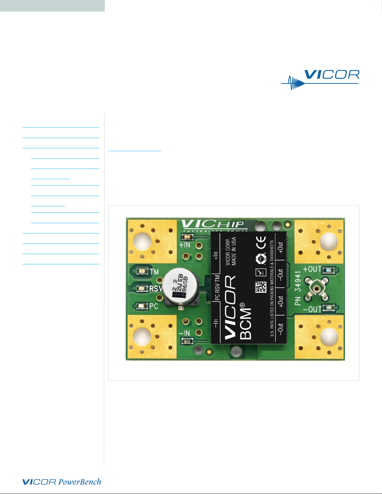
Please refer to Figure 1 for locations of the input and output connections as viewed from the
component side. Wires may be soldered directly to the pads instead of ring lugs if desired to minimize
circuit impedances.
Features
Oscilloscope probe jack for output voltage and ripple measurements
Simple to use
Ring lug or solder connections
Parallelable
UG:001 Page 1
Page 2
–
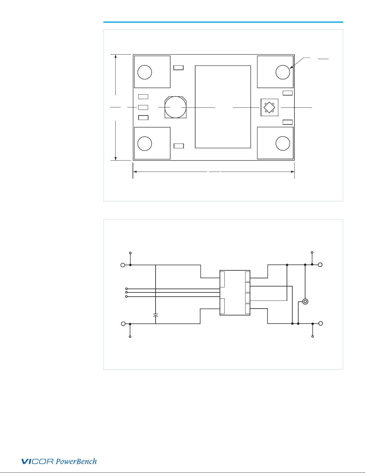
Figure 1
BCM® evaluation board
demo layout and dimensional
drawing, component side
1.65
41.9
TP2
TP1
TM
RSV
PC
+IN
C1
–IN
TP5
TP4
2.52
64,0
BCM
+OUT
J1
– OUT
TP7
TP6
Ø 0.20 Typ
5.08
C
L
Figure 2
BCM evaluation
board schematic
+IN
IN
TM
RSV
PC
C1
2.2 µF
450 V
+OUT
TP5
+In
TM
BCM
RSV
TP2
PC
TP1
TP4
-In
+Out
-Out
+Out
-Out
TP7
TP6
J1
–OUT
UG:001 Page 2
Page 3

Set Up
The evaluation board should be set up as follows.
Note: Care should be taken to avoid reversing polarities if connecting to the opposite (solder) side of the board.
+IN, –IN
Connect a high-quality, low-noise power supply to the +IN and –IN terminals of the evaluation board.
The interconnect leads should be heavy gauge and as short as possible. Additional capacitance may
have to be added on the evaluation board to make up for impedances in the interconnect leads as
well as deficiencies in the source. It is important to remember that noise from the source, as well as
any input source voltage drops, will appear at the output of the BCM® multiplied by its K factor. Test
points 4 (–IN) and 5 (+IN) can be used to monitor the input and are located on the PCB adjacent to the
input terminals.
+ OUT, –OUT
An electronic or passive load should be connected to +OUT and –OUT terminals of the evaluation
board with short heavy-gauge leads. Most commercially available electronic loads do not have current
slew rates capable of fully exercising the BCM. The evaluation board can be connected directly to
the application for which the BCM is intended. However, the interconnect impedances between
the evaluation board and the application can greatly affect the transient response. For applications
where transient response is critical, the user should consider mounting the BCM directly to the target
application PCB. Test points 6 (–OUT) and 7 (+OUT) can be used to monitor the output and are located
on the PCB adjacent to the output terminals.
Output Voltage Measurement Jack (J1)
This connector is provided to make accurate measurements of the output voltage of the BCM. Many
types of scope probes may be directly connected to this point if the probe is equipped with a removable
plastic sheath. To avoid creating ground loops when making measurements of the output or input
voltage, these measurements should be made separately.
Paralleling
The paralleling and current sharing capability of the devices can be demonstrated by stacking multiple
evaluation boards and interconnecting the inputs and outputs with standoffs of sufficient current
handling capability to create a 3-dimensional array. See Figure 3. When paralleling BCMs, the PC ports
should be connected together to ensure the outputs turn on simultaneously.
UG:001 Page 3
Page 4

Figure 3
BCM® evaluation:
paralleling connections of two
BCM evaluation boards
+IN
–IN
+OUT
–OUT
Input Current Measurement
A current probe can be passed around the +IN lead connected to the BCM. Input capacitors on the
evaluation board are downstream of this measurement point.
TM: Do not connect, for factory use only.
VC: Do not connect, for factory use only.
Primary Control (PC)
The PC can be used to disable the BCM, monitor status or provide a primary-referenced bias supply.
a. Connecting PC to the –IN will disable the BCM.
b. Connecting a DVM or oscilloscope between PC (positive) and –IN (negative) will indicate the
status of the BCM. Please note that the BCM does not have active current-sinking capability.
c. Connecting a load between PC (positive) and –IN (negative) will provide a
primary-referenced bias supply.
Efficiency Measurement
As the BCM can deliver and consume large currents, the effect of the PCB must be considered when
making an efficiency measurement. Be certain to accurately measure the voltage directly at the BCM
using the appropriate pair of contact points located at the corners of the BCM.
UG:001 Page 4
Page 5

Recommended Hardware
Table 1
Hardware
Quantity
4 ring lug Panduit LCA56-10-L
4 #10-32 screw
4 #10 flat washer
4 #10 lock washer
4 #10 hex nut
All hardware is stainless steel except the ring lug.
Kit # 26647 is included with the evaluation board.
Description Manufacturer P/N Vicor P/N
Kit #26647
}
Thermal
For most lab environments a fan blowing across the evaluation board is recommended.
See Application Note AN:008 or contact Vicor Applications Engineering for assistance.
Caution
The BCM® and evaluation board can comfortably operate at surface temperatures which may pose a
thermal hazard to the operator. Be careful not to touch any exposed surface. Certain BCMs may operate
at potentially dangerous voltages, use care in such cases. The evaluation board is not intended for use in
end item equipment.
Ordering Information
The BCM evaluation boards can be ordered from the Vicor website:
www.vicorpower.com.
To order the demo boards, substitute BCM with BCD in BCM part number.
See http://www.vicorpower.com/dc-dc/isolated-fixed-ratio/lv-bus-converter-module
for part number listing.
UG:001 Page 5
Page 6

Limitation of Warranties
Information in this document is believed to be accurate and reliable. HOWEVER, THIS INFORMATION
IS PROVIDED “AS IS” AND WITHOUT ANY WARRANTIES, EXPRESSED OR IMPLIED, AS TO THE
ACCURACY OR COMPLETENESS OF SUCH INFORMATION. VICOR SHALL HAVE NO LIABILITY FOR THE
CONSEQUENCES OF USE OF SUCH INFORMATION. IN NO EVENT SHALL VICOR BE LIABLE FOR ANY
INDIRECT, INCIDENTAL, PUNITIVE, SPECIAL OR CONSEQUENTIAL DAMAGES (INCLUDING, WITHOUT
LIMITATION, LOST PROFITS OR SAVINGS, BUSINESS INTERRUPTION, COSTS RELATED TO THE REMOVAL
OR REPLACEMENT OF ANY PRODUCTS OR REWORK CHARGES).
Vicor reserves the right to make changes to information published in this document, at any time
and without notice. You should verify that this document and information is current. This document
supersedes and replaces all prior versions of this publication.
All guidance and content herein are for illustrative purposes only. Vicor makes no representation or
warranty that the products and/or services described herein will be suitable for the specified use without
further testing or modification. You are responsible for the design and operation of your applications
and products using Vicor products, and Vicor accepts no liability for any assistance with applications or
customer product design. It is your sole responsibility to determine whether the Vicor product is suitable
and fit for your applications and products, and to implement adequate design, testing and operating
safeguards for your planned application(s) and use(s).
VICOR PRODUCTS ARE NOT DESIGNED, AUTHORIZED OR WARRANTED FOR USE IN LIFE SUPPORT,
LIFE-CRITICAL OR SAFETY-CRITICAL SYSTEMS OR EQUIPMENT. VICOR PRODUCTS ARE NOT CERTIFIED
TO MEET ISO 13485 FOR USE IN MEDICAL EQUIPMENT NOR ISO/TS16949 FOR USE IN AUTOMOTIVE
APPLICATIONS OR OTHER SIMILAR MEDICAL AND AUTOMOTIVE STANDARDS. VICOR DISCLAIMS
ANY AND ALL LIABILITY FOR INCLUSION AND/OR USE OF VICOR PRODUCTS IN SUCH EQUIPMENT OR
APPLICATIONS AND THEREFORE SUCH INCLUSION AND/OR USE IS AT YOUR OWN RISK.
Terms of Sale
The purchase and sale of Vicor products is subject to the Vicor Corporation Terms and Conditions of Sale
which are available at: (http://www.vicorpower.com/termsconditionswarranty)
Export Control
This document as well as the item(s) described herein may be subject to export control regulations.
Export may require a prior authorization from U.S. export authorities.
Contact Us: http://www.vicorpower.com/contact-us
Vicor Corporation
25 Frontage Road
Andover, MA, USA 01810
Tel: 800-735-6200
Fax: 978-475-6715
www.vicorpower.com
10/18
email
Customer Service: custserv@vicorpower.com
Technical Support: apps@vicorpower.com
©2018 Vicor Corporation. All rights reserved. The Vicor name is a registered trademark of Vicor Corporation.
All other trademarks, product names, logos and brands are property of their respective owners.
Rev 1.2 Page 6
Page 7

Mouser Electronics
Authorized Distributor
Click to View Pricing, Inventory, Delivery & Lifecycle Information:
Vicor:
BCD384F120T300A00
 Loading...