

Page 1
Cool-Power
®
PI33XX-XX
Multi-Phase Design Guide
1
out
in
in
in
R1
out
out
PGD
out
in
in
R1
out
PGD
1
2
3
2
(a) (b)
Description
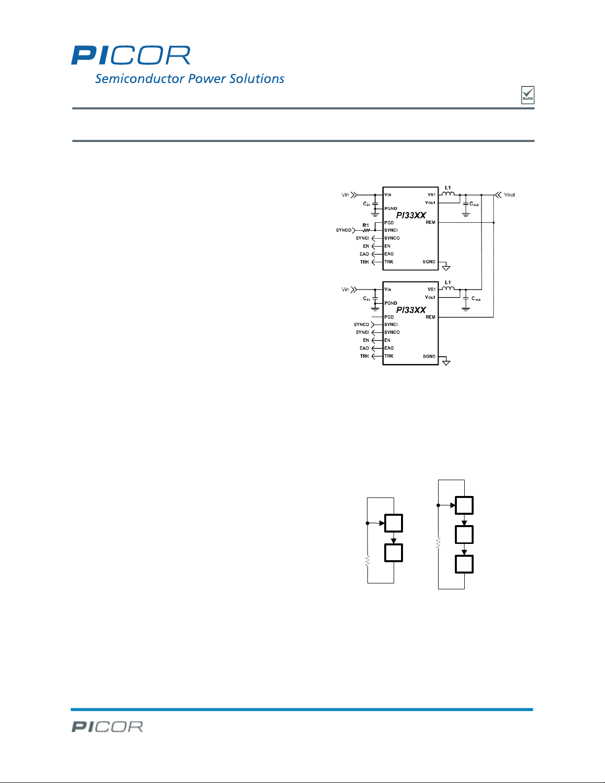
The Multi-Phase Design Guide provides an overview
to paralleling two or three PI33XX-XX devices
together without any change required to the basic
single-phase power stage or compensation design.
Paralleling multiple PI33XX modules increases the
output current capability and reduces the output
voltage ripple. For information on paralleling more
than three regulators, please contact Picor.
Basic Connections
The PI33XX family of Cool-Power products employs a
ZVS topology which operates exclusively in
discontinuous and critical conduction mode.
Therefore, to derive real-time output current
information, each device’s error amplifier output
(EAO) is trimmed to a nominal level (2.2V) when
supporting the maximum rated output load. This will
allow the EAO to track the output load. By trimming
the EAO this way, additional regulators can be
connected in parallel to deliver equal amount of
current to a single regulated point by linking each
regulator’s EAO pin together. The basic pin
connections needed to parallel two or three
regulators are shown in Figure 1. The SYNCO pins are
for phase synchronization, TRK is for soft-start and
fault shutdown tracking. EAO is for current sharing
between phases.
Figure 1 – Basic Connections for Parallel Operation
This method will allow the regulators to remain in
synchronization when the system’s operational
frequency stretches at high output loads. Figure 2
shows the basic synchronization connections and the
phase requiring delays in red.
Two and Three Phases
The PI33XX-2X can be synchronized in a closed loop
configuration to up to three phases by adding an
additional 2.5kΩ (R1) feedback resistor to the design
and incorporating the PGD pin.
vicorpower.com Rev 1.0 Cool-Power®
800 735.6200 11/2012 Page 1 of 4
Figure 2 - SYNCI (In) and SYNCO (Out) Connection for
Two and Three Phase Design
Page 2
Multi-Phase Design Guide
Sync Delay and Code
Regulator
1 2 3
2-phase
- -
3-phase
-
0Eh
1/3
0Eh
1/3
A[5]
A[4]
A[3]
A[2]
A[1]
A[0]
R/W
ADR1
ADR2
HEX
DEC
1 0 0 1 0 0 0 X 0 0 48
72
1 0 0 1 0 0 1 X 0
NC
49
73
1 0 0 1 0 1 0 X 0 1 4A
74
1 0 0 1 0 1 1 X NC 0 4B
75
1 0 0 1 0 0 0 X NC
NC
4C
76 1 0 0 1 1 0 1 X
NC 1 4D
77
1 0 0 1 1 1 0 X 1 0 4E
78 1 0 0 1 1 1 1 X 1 1+NC
4F
79
The required per phase delay and programming code
are presented in the following table.
Table 1 - Phase Programming Codes
Synchronization / Phase Delay
Two regulators connected in parallel operation do not
require any delay programming. As a default setting,
the PI33XX-XX will trigger on the falling edge and will
operate 180⁰ out of phase with the master. For a
three phase operation, a 1/3 phase delay is required
for two of the regulators to ensure proper phase
spacing. Synchronization and phase delay is only
programmable with I
2X).
2CTM
option regulators (PI33XX-
I2C Device Address
The PI33XX-2X supports floating addressing so that
two address lines allows for up to 8 programmable
addresses.
The address is 7 bit with the read/write bit not
included. Table 2 shows the address range that can
be achieved using all possible combinations of ADR0
(pad G1) and ADR1 (pad H1). Bits A[6]-A[3] are fixed
internally and may not be changed. The least
significant 3 bits; A[2]-A[0], will assume the values in
the table based on the decoding of ADR1 and ADR0. A
zero or one indicates the logic strength of the bit and
“NC” indicates that the pin is floating or not
connected. The HEX column indicates the final
address in hexadecimal, while the DEC column is the
decimal address value.
vicorpower.com Rev 1.0 Cool-Power®
800 735.6200 11/2012 Page 2 of 4
Table 2 - PI33XX-2X Device Addressing
Page 3

Multi-Phase Design Guide
Start
Addr.
Device
Wr Ack
Addr.
Reg
Ack Data
Ack Stop S XXh 1 0
20h 0 00h 0 P S XXh 1 0
21h 0 00h 0 P S XXh 1 0
22h 0 00h 0 P
Start
Adr.
Device
Wr Ack
Adr.
Reg
Ack Data
Ack Stop
S
XXh 1 0
18h 0 05h 0 P
Start
Adr.
Device
Wr Ack
Adr.
Reg
Ack
Data
Delay
Ack Stop S XXh 1 0
21h 0 0Eh 0 P
Start
Adr.
Device
Wr Ack
Adr.
Reg
Ack Data
Ack Stop S XXh 1 0
18h 0 00h 0 P
Programming Synchronization Delay
The PI33XX-2X provides an I2CTM Standard Mode
digital interface that enables the user to
program phase delays. This is a one-time
programmable option to the device. To set a
delay, the user needs to assign a unique Device
Address (see Table 2) to wake up the device
during programming. Then send the
synchronization delay address (21h) and the
delay data (OEh) while adhering to I2C protocols
and Figure 4 sequencing.
1) Clear all Registers to 00h with the device enabled
The following figure demonstrates the proper
steps to program a single phase-delay. The
device address is determined by the user and
the synchronization delay is provided in Table 1.
The device address is represented as XXh (Bold)
in Figure 6. Because this process in not
reversible, it is important to follow all steps in
Figure 4.
2) Enter Test Mode 5
3) Disable then Re-enable the Device (Enable Pin)
4) Set Desired Delay
5) Disable Device (Enable Pin)
6) Return to Test Mode 0
7) Repeat 1); Clearing all Registers
8) Enable Device (Enable Pin); Programming is Complete
Figure 4 - Showing the 8 Steps Required to Program a Single 1/3 Phase Delay
vicorpower.com Rev 1.0 Cool-Power®
800 735.6200 11/2012 Page 3 of 4
Page 4

Multi-Phase Design Guide
I2C is a Trademark of NXP Semiconductor
Kill Bit 2 Option
Once synchronization has been programmed, a Kill
bit located at address 22h can be burned, to 01h, to
prevent any future erroneous blowing of remaining
zero bits. The programming protocol is the same as
shown above (Figure 4) except for step 4). Change
the Address Register to 22h and the Data sent to
01h.
For more detailed I2C interfacing information and
available software please refer to the “PI33XX-2X I2C
Digital Interface Guide.”
vicorpower.com Rev 1.0 Cool-Power®
800 735.6200 11/2012 Page 4 of 4
 Loading...