

Page 1
Introduction
The PI2003-EVAL1 allows the user to test the basic principle
and operational characteristics of a low side Active ORing
function in a redundant power architecture, while also
experiencing the benefits and value of the PI2003 solution
versus conventional Active ORing solutions. The PI2003-EVAL1
evaluation board is configured to receive two independent
power source inputs, per a typical redundant power
architecture, through two Active ORing channels that are
combined to form a redundant power output. Each channel
contains a PI2003 controller and an N-channel power
MOSFET. The MOSFET foot print can take an SO-8 or Power
SO-8 MOSFET package. Each channel is capable of up to 6 A.
The PI2003-EVAL1 evaluation board is designed with
optimized PCB layout and component placement to represent
a realistic high density final design for an embedded low side
Active ORing solution for -48 Vbus applications requiring up
to 6 A. This evaluation board is intended as an easy and
simple way to test the electrical and thermal performance of
the PI2003 Active ORing controller.
Both dynamic and steady state testing of the PI2003 can be
completed on the PI2003-EVAL1 evaluation board, in addition
to using the key features of the product. Dynamic testing can
be completed under a variety of system level fault conditions
to check for response time to faults.
This document provides basic instructions for initial start-up
and configuration of the evaluation board. Further
information on the functionality of the PI2003 can be
found in the PI2003 product data sheet.
PI2003-EVAL1
Cool-ORing™ Series
PI2003-EVAL1 Active ORing
Evaluation Board User Guide
®
Contents
Introduction . . . . . . . . . . . . . . . . . . . . . . . . . . . . . . Page 1
PI2003 Product Description . . . . . . . . . . . . . . . . . . Page 2
Evaluation Board Terminal Description . . . . . . . . Page 2
Evaluation Board Schematic . . . . . . . . . . . . . . . . . Page 3
Bill of Materials . . . . . . . . . . . . . . . . . . . . . . . . . . . Page 3
Test Procedure . . . . . . . . . . . . . . . . . . . . . . . . . . . . Page 4
PCB Layouts . . . . . . . . . . . . . . . . . . . . . . . . . . . . . . Page 7
Evaluation Board Mechanical Drawing . . . . . . . . Page 7
PI2003-EVAL1 Evaluation Board
featuring the Cool-ORing PI2003
Active ORing controller.
Cool-ORing™ Series
The PI2003-EVAL1 Evaluation Board is intended to acquaint the
user with the benefits and features of the Cool-ORing
TM
PI2003
full function Active ORing solution. It is not designed to be
installed in end-use equipment.
Please read this document before setting up the PI2003-EVAL1
Evaluation Board and refer to the PI2003 product data sheet
for device specifications, functional description and
characteristics.
During operation, the power devices and surrounding
structures can be operated safely at high temperatures.
• Remove power and use caution when connecting and
disconnecting test probes and interface lines to avoid
inadvertent short circuits and contact with hot surfaces.
• When testing electronic products always use approved
safety glasses. Follow good laboratory practice and
procedures.
Picor Corporation • www.picorpower.com PI2003-EVAL1 User Guide Rev 1.0 Page 1 of 8
Page 2
The Cool-ORing PI2003 with an external industry standard
100V N-channel MOSFET provides a complete Active ORing
solution designed for use in -48 Vbus redundant power
system architectures. The PI2003 controller with an N-channel
MOSFET enables extremely low power loss with fast dynamic
response to fault conditions, critical for high availability
systems.
The PI2003 controller with a low Rds(on) N-channel MOSFET
provides very high efficiency and low power loss during
steady state operation. The PI2003 controller provides an
active low fault flag output to the system during excessive
forward current, light load, or reverse current.
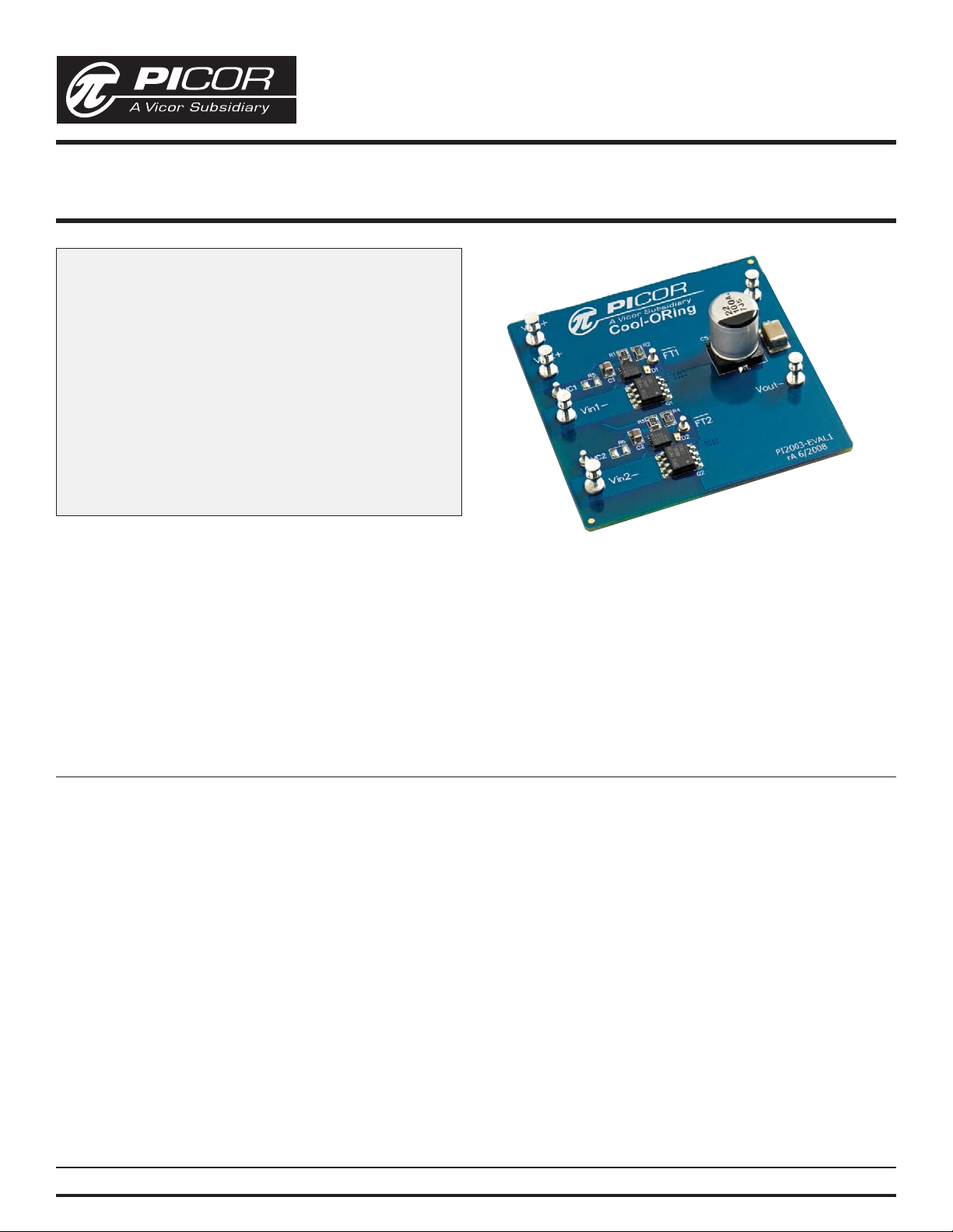
Figure 1 shows a photo of the PI2003-EVAL1 evaluation
board, with two PI2003 controllers and two N-channel
MOSFET used to form the two Active ORing channels. The
board is built with two identical Active ORing circuits with
options and features that enable the user to fully explore the
capabilities of the PI2003 universal Active ORing controller.
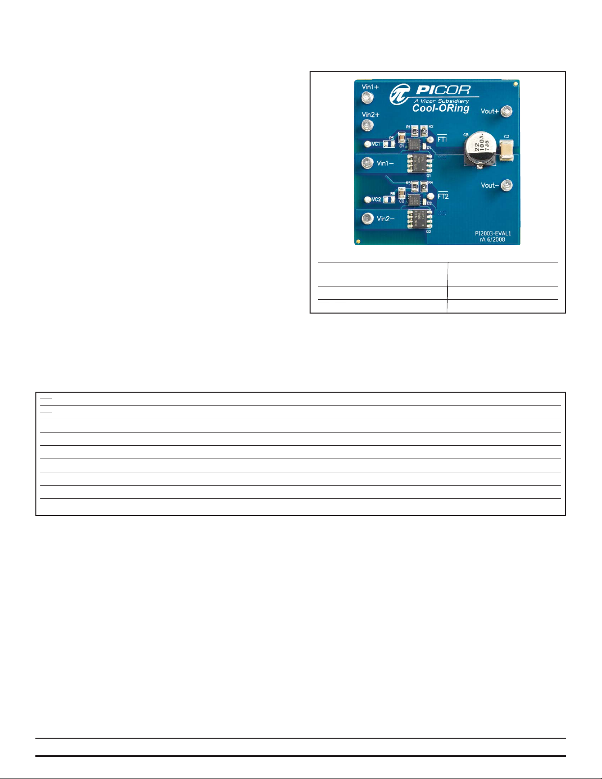
Figure 1 – PI2003 -EVAL1 Evaluation Board (1.8" x 1.8")
Terminals Rating
Vin1+ to Vin1-, 60 V / 8 A
Vin2+ to Vin2- 60 V / 8 A
VC1, VC2 -0.3 V to 17.3 V / 40 mA
FT1, FT2 -0.3 V to 17.3 V / 10 mA
Terminal Description
Vin1+ and Vin1- Power Source Input #1: or bus input designed to accommodate up to 60 V and 6 A continuous current.
Vin1+ and Vin1- Power Source Input #2: or bus input designed to accommodate up to 60 V and 6 A continuous current.
VC1 Optional Auxiliary Input Voltage #1: to supply PI2003 VC power. VC1 should be 10 V or higher to fully enhance the MOSFET.
VC2 Optional Auxiliary Input Voltage #1: to supply PI2003 VC power. VC1 should be 10.V or higher to fully enhance the MOSFET.
FT1 PI2003 (U1) Fault Pin: Monitors U1 fault conditions
FT2 PI2003 (U2) Fault Pin: Monitors U2 fault conditions
Vout + Output +: connected to input return
Vout- Output -: connected to MOSFETs sources
Table 1 – PI2003-EVAL1 Evaluation Board terminals description
Cool-ORingTMPI2003 Product Description
Picor Corporation • www.picorpower.com PI2003-EVAL1 User Guide Rev 1.0 Page 2 of 8
Page 3
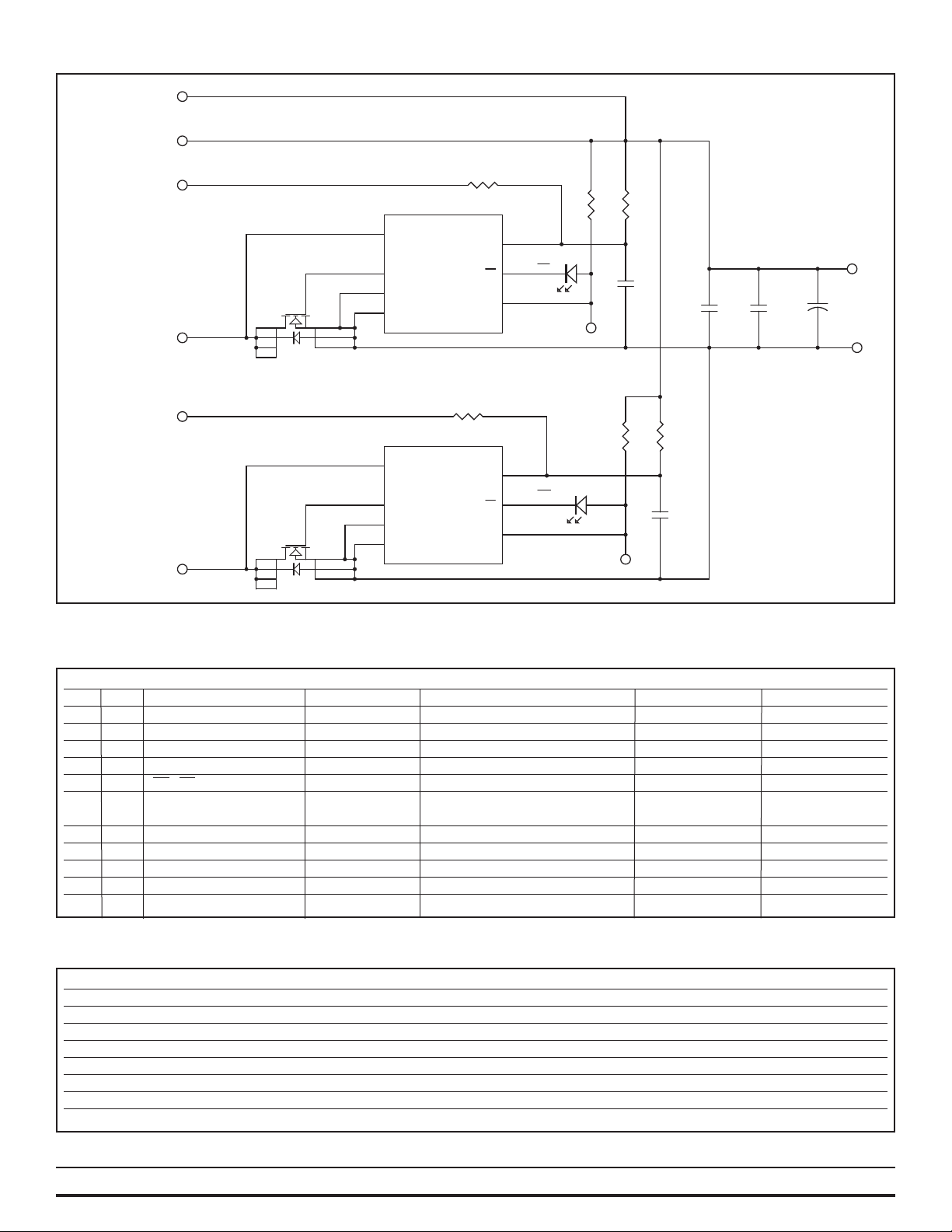
Vin1+
Figure 2 – PI2003-EVAL1 Evaluation Board schematic.
Item QTY Reference Designator Value Description Footprint Manufacturer
1 2 C1, C2 1 µF Capacitor, MLCC X5R, 1 µF,16 V 0603
2 1 C3 2.2 uF Capacitor, MLCC X7R, 2.2 uF, 100 V 1812
C4 Not installed 1812
C5 22 µF Capacitor, Electrolytic, 22 µF 100 V
4 2 D1, D2 LED, Super Red THIN 0603 Lite-On, Inc.,
5 4 FT1, FT2, VC1, VC2 Turret Test point TURRET-1528 Keystone Electronics
66
Vin1+, Vin1-, Vin2+, Vin2-,
Turret Test point TURRET-1502 Keystone Electronics
Vout+, Vout9 2 Q1, Q2 IRF7853 100 V, 8.3 A, N-MOSFET SO-8 International Rectifier
10 2 R1, R3 11 KΩ Resistor, 11 KΩ,1/4 W, 5% 0805
11 2 R2, R4 24 KΩ Resistor, 24 KΩ,1/8 W, 5% 0805
12 2 R5, R6 Not Installed 0805
16 2 U1, U2 PI2003 Picor Active ORing Controller 3mmx3mm; 10-TDFN PICOR
Table 2 – PI2003-EVAL1 Evaluation Board bill of materials
Reference Designator Value Functional Description
C1, C2 1 uF VC Bypass Capacitor
C3, C4, C5, Output (Load) Capacitor
D1, D2 LED To indicate a fault exists when it is on
Q1, Q2 N-MOSFET ORing MOSFET
R1, R3 11 KΩ VC Bias resistor
R2, R4 24 KΩ LED current limit resistor
R5, R6 Not Installed Optional to connect VC to separate source
U1, U2 PI2003 Picor Active ORing Controller
Table 3 – Component functional description
Picor Corporation • www.picorpower.com PI2003-EVAL1 User Guide Rev 1.0 Page 3 of 8
BUS(+) A
Vin2+
VC1
Vin1-
Vin2-
VC2
BUS(+) B
BUS(- ) A
BUS(- ) B
Q1
IRF7853
5
6
7
8
Q2
IRF7853
5
6
7
8
R5
D1
VC2
R2
R1
24K
11k
C1
1uF
FT1
R4
R3
24K
11k
D2
C2
1uF
FT2
C3
2.2uF
C4
Not Installed
Vout+
C5
22uF
Vout-
PI2003
Not Installed
PI2003
Not Installed
VC
FT
FC
R6
VC
FT
FC
3
VC1
6
FT1
5
3
FT2
6
5
U1
8
SN
2
GATE
7
4
1
2
3
4
1
2
3
SP
1
GND
U2
8
SN
2
GATE
7
SP
1
GND
Page 4

Initial Test Set Up
Baseline Test Procedure (Refer to Figure 3)
1.0 Recommended Equipment
1.1 Two Isolated DC power supplies - 0 – 60 V; 10 A
1.1.1 If the DC power supply outputs are not isolated,
two 10 A 100 V Schottky diodes are required,
as shown in Figure 4.
1.2 DC electronic load - 10 A minimum.
1.3 Digital Multimeter
1.4 Oscilloscope.
1.5 Appropriately sized interconnect cables.
1.6 Safety glasses.
1.7 PI2003 Product Data sheet.
Figure 3 – Layout configuration for a typical redundant power application, using isolated power supplies.
Figure 4 – Layout configuration for a typical redundant power application, using non-isolated power supplies.
Picor Corporation • www.picorpower.com PI2003-EVAL1 User Guide Rev 1.0 Page 4 of 8
Page 5

Before initial power-up follow these steps to configure the
evaluation board for specific end application requirements:
2.0 Controller Bias Voltage (VC):
2.1 The PI2003 Controller has a separate input (VC) that
provides power to the control circuitry and the gate
driver. An internal voltage regulator (VC) clamps the
VC voltage to 11 V typically. PI2003 EVAL1 is
configured to bias the controllers directly from the
bus voltage (Vin1 and Vin2). Two bias resistors
(R1 and R3: 11 kΩ, 1/4 W, 0805) are connected from
the return input (Vin1+ and Vin2+) to each controller
VC pin, see schematic in figure 2. The bias resistors
are selected to support -48 V bus voltage (36 V to 60 V).
2.2 If the bus voltage (Vin1 and Vin2) range is
different from 36 V to 60 V and higher than the
Clamp voltage, 11 V typical, the Rbias value has
to be changed using the following equations:
2.2.1 Select the value of Rbias using the
following equations:
Rbias =
Vbus
min –VCclampMAX
ICmax
2.2.2 Calculate Rbias maximum power
dissipation:
Pd
Rbias =
(Vbus
max –VCclampMIN )
2
Rbias
Where:
Vbus
min : V(bus) minimum voltage
Vbus
max : V(bus) maximum voltage
VC
clampMAX : Maximum controller clamp
voltage, 12 V
VC
clampMIN : Minimum controller clamp
voltage, 10 V
IC
MAX : Controller maximum bias current,
use 2.0 mA
2.2.3 For example, if the minimum
V(bus) = 36 V and the maximum
V(bus) = 60 V
Rbias =
Vbus
min –VCclampMAX
ICMAX
Rbias =
36 V – 12 V
= 12 KΩ
2.0 mA
Rbias maximum power dissipation is at maximum
input voltage.
PD
Rbias =
(Vbus
max –VCclampMIN)
2
=
(60 V – 10 V)
2
= 208 mW
Rbias 12 KΩ
2.3 The PI2003-EVAL1 is configured to allow the customer
to use a direct bias voltage to the controller VC pin
independent of the bus input. VC1 and VC2 terminals
can be connected directly to the controller VC pins
after removing R1 and R3 and populating R5 and R6.
3.0 Hook Up of the Evaluation Board,
refer to Figures 3 and 4.
3.1 If isolated power supplies are used, Figure 3.
3.1.1. Connect the positive terminal of PS1 power
supply to Vin1+. Connect the negative terminal
of PS1 Vin1-. Set the power supply to 48 V.
Keep PS1 output disabled (OFF).
3.1.2. Connect the positive terminal of PS2 power
supply to Vin2+. Connect the negative terminal
of PS2 Vin2-. Set the power supply to 48 V.
Keep PS2 output disabled (OFF).
3.2 If non-isolated power supplies are used, Figure 4.
3.2.1. Connect the positive terminal of PS1 power
supply to Vin1+ through a Schottky diode.
Connect the negative terminal of PS1 Vin1-.
Set the power supply to 48 V. Keep PS1 output
disabled (OFF).
3.2.2. Connect the positive terminal of PS2 power
supply to Vin2+ through a Schottky diode.
Connect the negative terminal of PS2 Vin2-.
Set the power supply to 48 V. Keep PS2 output
disabled (OFF).
Picor Corporation • www.picorpower.com PI2003-EVAL1 User Guide Rev 1.0 Page 5 of 8
Page 6

Figure 5 – Plot of PI2003 response time to reverse current detection
Picor Corporation • www.picorpower.com PI2003-EVAL1 User Guide Rev 1.0 Page 6 of 8
3.3 Connect the electronic load to the output between
Vout and Gnd. Set the load current to 1 A.
3.4 Enable (turn ON) PS1 power supply output.
3.5 Turn on the electronic load.
3.6 Measure the voltage across Q1, connect a voltmeter
between Vout- and Vin1-, the voltmeter should read
less than 30 mV to assure that the MOSFET is fully
enhanced.
3.7 LED D1 should be off indicating that controller U1 has
no fault. LED D2 should be on indicating that U2 is in
a fault mode and the controller Gate pin output
is low.
3.8 Disable (turn OFF) PS1 power supply output.
3.9 Enable (turn ON) PS2 power supply output.
3.10 Measure the voltage across Q2, connect a voltmeter
between Vout- and Vin2-, the voltmeter should read
less than 30mV to assure that the MOSFET is fully
enhanced.
3.11 LED D2 should be off indicating that controller U2 has
no fault. LED D1 should be on indicating that U1 is in
a fault mode and the controller Gate pin output is
low.
3.12 Enable (turn ON) PS1 and PS2.
3.13 Increase output load to 5 A. The power source, PS1
and PS2, should share the load current equally if
there output voltages are equal. Both LEDs, D1 and
D2, should be off indicating that both controllers
Gate pin output is high.
4.0 Input short circuit test
4.1 Apply a short at one of the inputs (Vin1 or Vin2). The
short can be applied electronically using a MOSFET
connected between low side off the source (Vin1- or
Vin2-) and the return (Vin1+ or Vin2+) or simply by
connecting Vin- to the return. Measure the response
time between when the short is applied and the
MOSFET Gate turns off. An example for PI2003
response time to an input short circuit is shown in
Figure 5.
Page 7

Picor Corporation • www.picorpower.com PI2003-EVAL1 User Guide Rev 1.0 Page 7 of 8
Mechancial Drawing
Figure 6a – PI2003-EVAL1 layout top layer. Scale 2.0:1 Figure 6b – PI2003-EVAL1 layout Bottom layer. Scale 2.0:1
1.800
1.600
1.300
1.100
0.895
0.500
0.295
0.000
Vin1+
Vin2+
VC1
VC2
Vin1-
Vin2-
1.800
Cool-ORing
R1
R5
C1
R3
R6
C2
R2
FT1
D1
Q1
R4
FT2
D2
Q2
Vout+
C5
Vout-
C3
C4
PI2003-EVAL1
rA 6/2008
1.450
1.145
0.650
0.535
0.000
0.000
0.150
0.830
1.650
1.800
Page 8

Vicor’s comprehensive line of power solutions includes high-density AC-DC & DC-DC
modules and accessory components, fully configurable AC-DC & DC-DC power supplies,
and complete custom power systems.
Information furnished by Vicor is believed to be accurate and reliable. However, no responsibility
is assumed by Vicor for its use. No license is granted by implication or otherwise under any patent
or patent rights of Vicor. Vicor components are not designed to be used in applications, such as
life support systems, wherein a failure or malfunction could result in injury or death. All sales are
subject to Vicor’s Terms and Conditions of Sale, which are available upon request.
Specifications are subject to change without notice.
Vicor Corporation
25 Frontage Road
Andover, MA 01810
USA
Picor Corporation
51 Industrial Drive
North Smithfield, RI 02896
USA
Customer Service: custserv@vicorpower.com
Technical Support: apps@vicorpower.com
Tel: 800-735-6200
Fax: 978-475-6715
Picor Corporation • www.picorpower.com PI2003-EVAL1 User Guide Rev 1.0 Page 8 of 8
 Loading...