

Page 1
Picor Corporation • www.picorpower.com PI2002-EVAL1 User Guide Rev 1.0 Page 1 of 11
Introduction
The PI2002-EVAL1 allows the user to test the basic principle
and operational characteristics of an Active ORing with Load
Disconnect function in a redundant power architecture, while
also experiencing the benefits and value of the PI2002
solution versus conventional Active ORing solutions. The
PI2002-EVAL1 evaluation board is configured to receive two
independent power source inputs, per a typical redundant
power architecture, through two Active ORing channels
that are combined to form a redundant power output.
Each channel contains a PI2002 controller and two N-channel
power MOSFETs (configured back-to-back). The MOSFET
footprints can take SO-8 or Power SO-8 MOSFET packages.
Each channel is capable of up to 20 A.
The PI2002-EVAL1 evaluation board is designed with
optimized PCB layout and component placement to represent
a realistic high density final design for an embedded Active
ORing with Load Disconnect solution for ≤ 7 Vbus
applications requiring up to 20 A. This evaluation board is
intended as an easy and simple way to test the electrical and
thermal performance of the PI2002 Active ORing with Load
Disconnect controller.
Both dynamic and steady state testing of the PI2002 can be
completed on the PI2002-EVAL1 evaluation board, in addition
to using the key features of the product. Dynamic testing can
be completed under a variety of system level fault conditions
to check for response time to faults.
This document provides basic instructions for initial start-up
and configuration of the evaluation board. Further
information on the functionality of the PI2002 can be
found in the PI2002 product data sheet.
PI2002-EVAL1
Cool-ORing™ Series
PI2002-EVAL1 Active ORing With Load Disconnect
Evaluation Board User Guide
®
Contents
Introduction . . . . . . . . . . . . . . . . . . . . . . . . . . . . . . Page 1
PI2002 Product Description . . . . . . . . . . . . . . . . . . Page 2
Evaluation Board Terminal Description . . . . . . . . Page 2
Evaluation Board Schematic . . . . . . . . . . . . . . . . . Page 3
Bill of Materials . . . . . . . . . . . . . . . . . . . . . . . . . . . Page 3
Evaluation Board Configuration . . . . . . . . . . . . . . Page 4
Test Procedure . . . . . . . . . . . . . . . . . . . . . . . . . . . . Page 4
PCB Layouts . . . . . . . . . . . . . . . . . . . . . . . . . . . . . Page 10
Evaluation Board Mechanical Drawing . . . . . . . Page 10
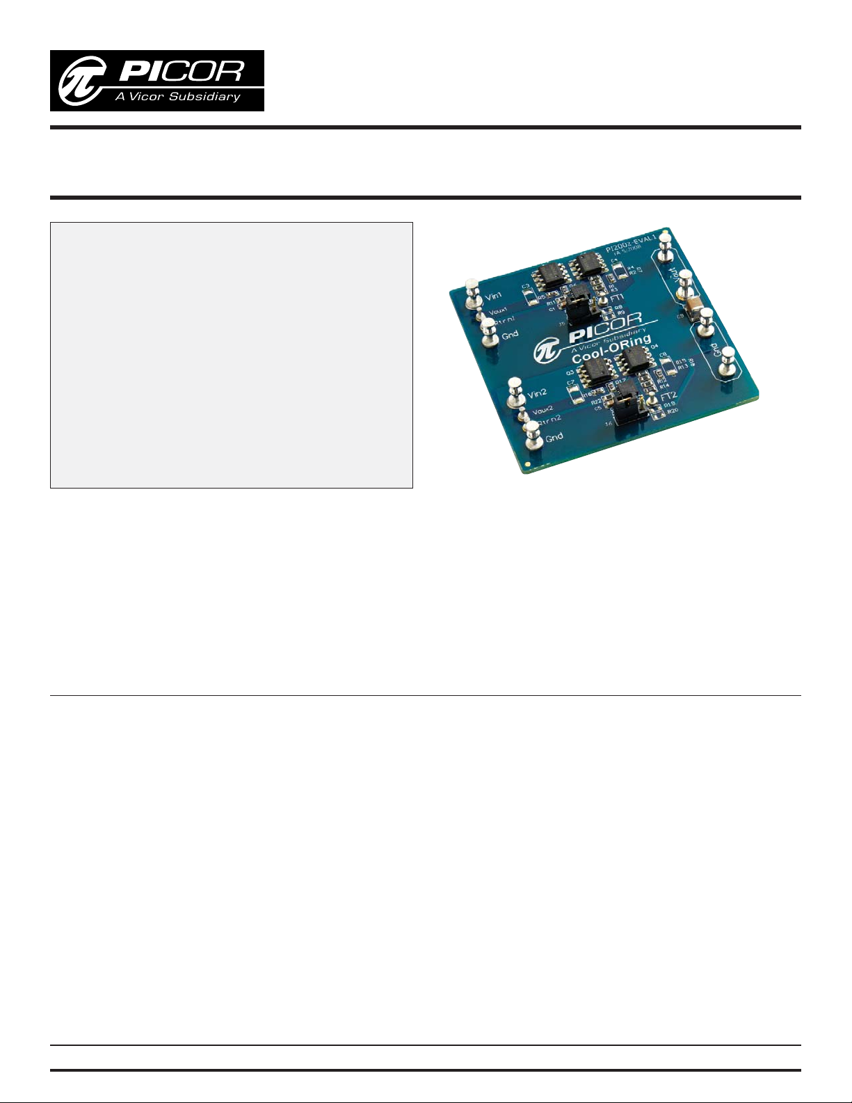
PI2002-EVAL1 Evaluation Board
featuring the Cool-ORing PI2002
Active ORing controller.
Cool-ORing™ Series
The PI2002-EVAL1 Evaluation Board is intended to acquaint the
user with the benefits and features of the Cool-ORing
TM
PI2002
Active ORing with Load Disconnect solution. It is not designed to
be installed in end-use equipment.
Please read this document before setting up the PI2002-EVAL1
Evaluation Board and refer to the PI2002 product data sheet
for device specifications, functional description and
characteristics.
During operation, the power devices and surrounding
structures can be operated safely at high temperatures.
• Remove power and use caution when connecting and
disconnecting test probes and interface lines to avoid
inadvertent short circuits and contact with hot surfaces.
• When testing electronic products always use approved
safety glasses. Follow good laboratory practice and . .
procedures.
Page 2
Picor Corporation • www.picorpower.com PI2002-EVAL1 User Guide Rev 1.0 Page 2 of 11
The Cool-ORing™ PI2002 with two external back-to-back
configured industry standard N-channel MOSFETs is a
complete Active ORing solution that also provides a Load
Disconnect feature designed for use in redundant power
system architectures. The PI2002 controls back-to-back
MOSFETs providing true bi-directional switch capabilities to
protect against both power source and load fault conditions.
The gate drive output turns the MOSFETs on in normal steady
state operation, while achieving high-speed turn-off under
a variety of potential system-level fault conditions, per
conventional Active ORing solutions with auto-reset once
the fault clears. The PI2002 has the added benefit of being
able to protect against output load fault conditions that
may induce excessive forward current and device overtemperature by removing gate drive from the MOSFETs
with an auto-retry programmable off-time. The back-to-back
MOSFETs drain-to-drain voltage is monitored to detect
normal forward, excessive forward, light load and reverse
current flow. The PI2002 provides an active low fault flag
output to the system during excessive forward current,
reverse current, light load, under-voltage, over-voltage and
over-temperature. A temperature sensing function turns
off the MOSFETs and indicates a fault if the junction
temperature exceeds 145°C.
Figure 1 shows a photo of the PI2002-EVAL1 evaluation
board, with two PI2002 controllers and four N-channel
MOSFETs used to form the two Active ORing channels that
also feature a Load Disconnect function. The board is built
with two identical Active ORing circuits with options and
features that enable the user to fully explore the capabilities
of the PI2002 universal Active ORing with Load Disconnect
controller.
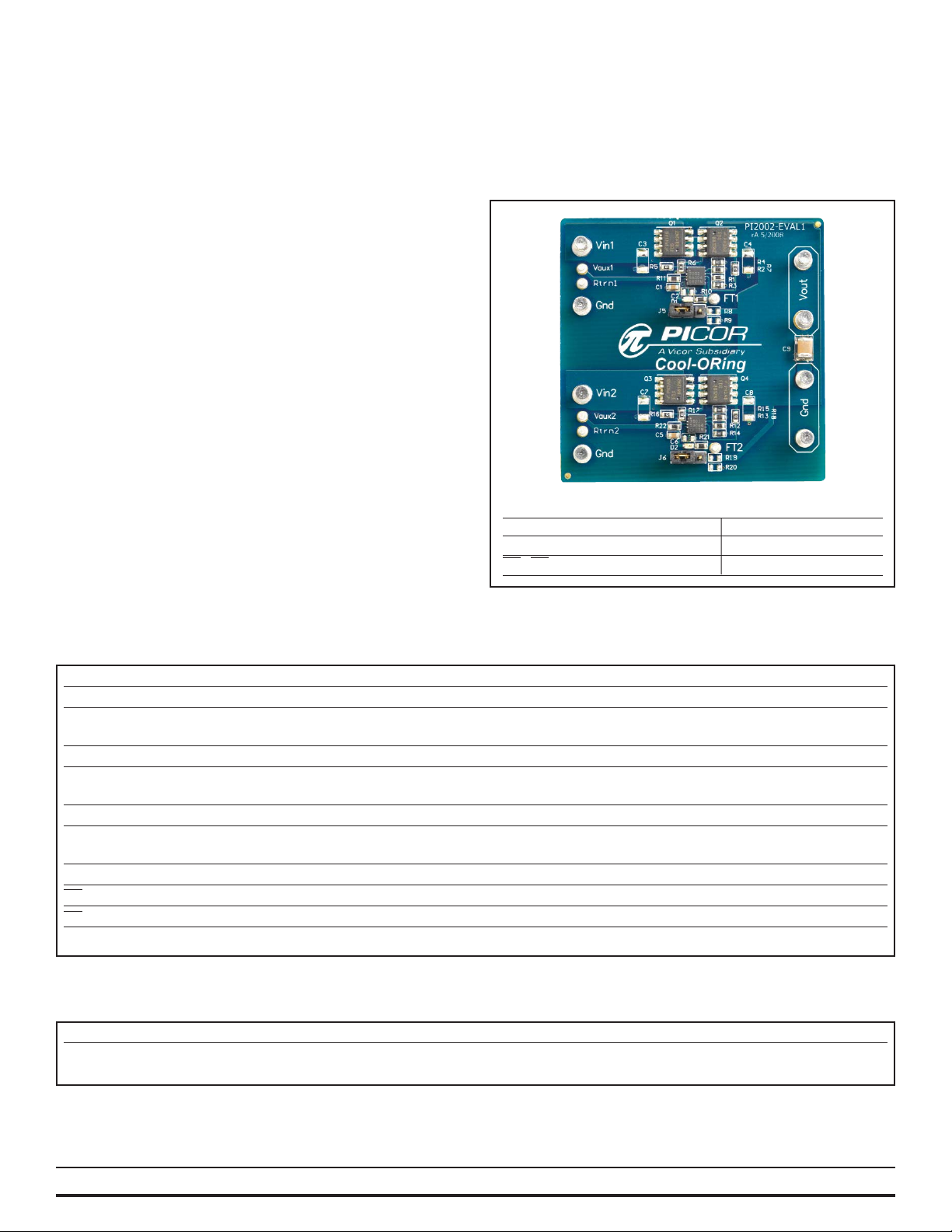
Figure 1 – PI2002-EVAL1 Evaluation Board (1.8" x 1.8")
Terminals Rating
Vin1, Vin2 8 V / 20 A
Vaux1, Vaux2, (R11 = R19 = 10 Ω) -0.3 V to 17.3 V / 40 mA
FT1, FT2 -0.3 V to 17.3 V / 10 mA
Terminal Description
Vin1 Power Source Input #1 or bus input designed to accommodate up to 20 A continuous current.
Vaux1 Auxiliary Input Voltage #1 to supply PI2002 VC power. Vaux1 should be equal to Vin1 plus 5 V or higher.
See details in Auxiliary Power Supply (Vaux) section of the PI2002 data sheet.
Rtn1 Vaux1 Return Connection: Connected to Ground plane
Gnd Vin & Vout Return Connection: Three Gnd connections are available and are connected to a common point, the Ground
plane. Input supplies Vin1 & Vin2 and the output load at Vout should all be connected to their respective local Gnd connection.
Vin2 Power Source Input #2 or bus input designed to accommodate up to 20 A continuous current.
Vaux2 Auxiliary Input Voltage #2 to supply PI2002 VC power. Vaux2 should be equal to Vin2 plus 5 V or higher.
See details in Auxiliary Power Supply (Vaux) section of the PI2002 data sheet.
Rtn2 Vaux2 Return Connection: Connected to Ground plane
FT1 PI2002 (U1) Fault Pin: Monitors U1 fault conditions
FT2 PI2002 (U2) Fault Pin: Monitors U2 fault conditions
Vout Output: Q2 and Q4 MOSFET Drain pins connection, connect to the load high side.
Table 1 – PI2002-EVAL1 Evaluation Board terminals description
Cool-ORingTMPI2002 Product Description
Jumper Description
J5, J6 SCD Jumpers: Connect jumper across the two pins to the input side (GND) for maximum Gate charge current or across
the two pins on the output side to connect to the resistive voltage divider to the output.
Table 2 – PI2002-EVAL1 Evaluation Board jumpers description
Page 3
Picor Corporation • www.picorpower.com PI2002-EVAL1 User Guide Rev 1.0 Page 3 of 11
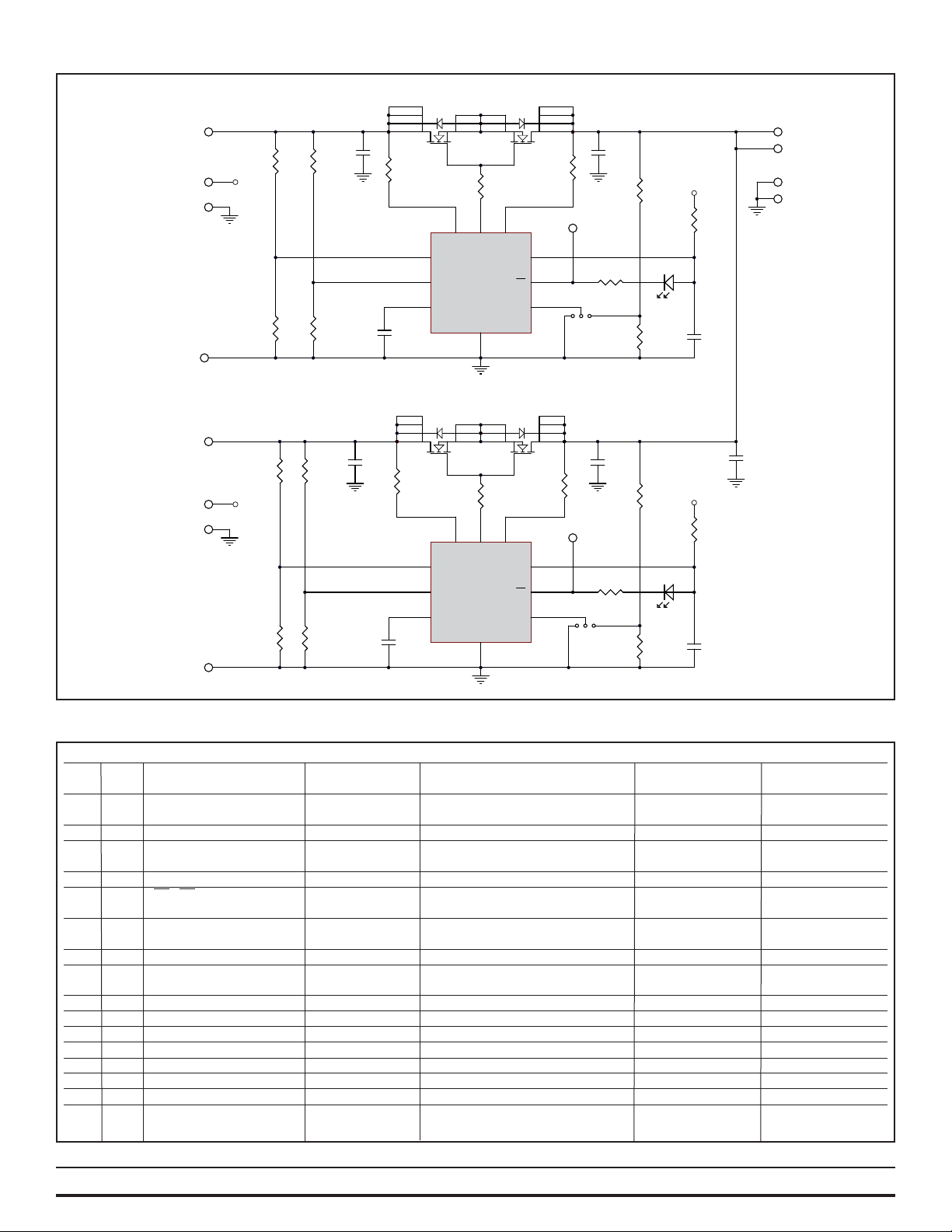
Vin1
Figure 2 – PI2002-EVAL1 Evaluation Board schematic.
Item QTY Reference Designator Value Description Footprint Manufacturer
1 2 C1, C2 1 µF
Capacitor, MLCC X5R,
0603
1 µF,16 V
2 1 C9 22 µF
Capacitor, MLCC X7R,
1210
22 µF, 25 V
3 4 C3, C4, C7, C8 Not installed 1206
4 2 C2, C3 18 nF
Capacitor, MLCC X5R,
0603
18 nF,25 V
5 2 D1, D2 LED, Super Red THIN 0603 Lite-On, Inc.,
66
FT1, FT2, Rtn1, Rtn2,
Turret Test point TURRET-1528
Keystone
Vaux1, Vaux2 Electronics
78
Gnd1, Gnd2, Gnd3, Gnd4,
Turret Test point TURRET-1502
Keystone
Vin1, Vin2, Vout1, Vout2 Electronics
8 2 J5, J6 Header Pins 0.1" pitch 2 x 3mm
9 4 Q1, Q2, Q3, Q4
FDS8812NZ
SO-8 Fairchild
30 V, 20 A, N-MOSFET
10 2 R1, R12 8.45 KΩ Resistor,8.45 KΩ,1% 0603
11 2 R2, R13 13.3 KΩ Resistor,13.3 KΩ,1% 0603
12 4 R3, R4, R14, R15 2.00 Ω Resistor, 2.00 Ω, 1% 0603
13 6 R5, R6, R7, R16, R17, R18 0 Ω Resistor, 0 Ω 0603
14 2 R8, R9, R19, R20 Not Installed 0603
15 2 R10, R21 4.99 kΩ Resistor, 4.99 Ω, 5% 0603
16 2 R11, R22 10 Ω Resistor, 10 Ω, 5% 0603
17 2 U1, U2 PI2002
Picor Active ORing 3 mm x 3 mm;
PICOR
with Load Disconnect Controller 10-TDFN
Table 3 – PI2002-EVAL1 Evaluation Board bill of materials
Vaux1 Vaux1
Gnd1
Rtrn1
R1
8.45K
1%
R3
2.00k
1%
R2
13.3k
1%
R4
2.00k
1%
Not Installed
Q1
FDS8812NZ
8
7
6
5
C3
R5
0
C2
18nF
3
2
1
4
7
SP
9
UV
10
OV
4
OCT
Q2
FDS8812NZ
3
2
1
R6
5
2
G
D
N
G
1
8
7
6
5
4
8
IC1
PI2002
SN
3
VC
6
FT
5
SCD
C4
R7
Not Installed
0
FT1
VC1
R10
FT1
4.99K
J5
Not Installed
R9
VoutVin1
R8
Not Installed
Red LED
D1
Vaux1
R11
10
C1
1uF
Out1
Out2
Gnd3
Gnd4
Q4
DS8812NZ
F
3
2
1
R17
5
2
G
GND
1
8
7
6
5
C5
1uF
C9
22uF
4
8
IC2
PI2002
SN
3
VC
6
FT
5
SCD
R18
FT2
C8
Not Installed
VC2
R21
4.99K
R20
Not Installed
R19
Not Installed
Red LED
D2
Vaux2
R22
10
0
FT2
J6
Vin2
Vaux2 Vaux2
Gnd2
Rtrn2
Vin2
R12
8.45k
1%
R14
2.00k
1%
R13
13.3k
1%
R15
2.00k
1%
C7
Not Installed
R16
C6
18nF
0
8
7
6
5
9
10
4
Q3
FDS8812NZ
4
7
UV
OV
OCT
3
2
1
SP
Page 4
Initial Test Set Up
To test the PI2002-EVAL1 evaluation board it is necessary to
configure the jumpers (J5 and J6) first based on the required
board configuration.
Failure to configure the jumpers prior to the testing may
result in improper circuit behavior.
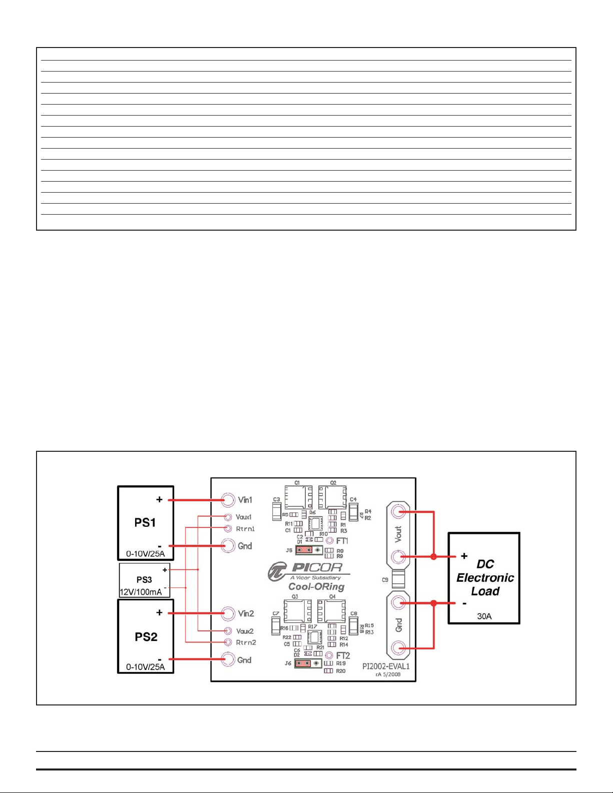
Baseline Test Procedure (Refer to Figure 3)
1.0 Recommended Equipment
1.1 Two DC power supplies - 0-10 V; 25 A.
1.2 DC power supply 12 V; 100 mA.
1.3 DC electronic load - 30 A minimum.
1.4 Digital Multimeter
1.5 Oscilloscope.
1.6 Appropriately sized interconnect cables.
1.7 Safety glasses.
1.8 PI2002 Product Data sheet.
Figure 3 – Layout configuration for a typical redundant power application, OCD configured for fast gate turn on.
Picor Corporation • www.picorpower.com PI2002-EVAL1 User Guide Rev 1.0 Page 4 of 11
Reference Designator Value Functional Description
C1, C5 1 µF VC Bypass Capacitor
C9 22 µF Output (Load) Capacitor
C3, C4, C7, C8 Not installed Snubber to reduce voltage ringing when the device turns off
C2, C6 18 nF OCT off timer Capacitor
D1, D2 LED To indicate a fault exist when it is on
J5, J6 Jumper SCD to select for Gate high charge current or Gate low charge current
Q1, Q2, Q3, Q4 N-MOSFET ORing Main Switch
R1, R12 8.45 KΩ UV Voltage Divider Resistor ( R2UV in Figure 4)
R2, R13 13.3 KΩ OV Voltage Divider Resistor ( R2OV in Figure 4)
R11, R22 10 Ω VC Bias resistor
R10, R21 4.99 KΩ LED Current Limiter
R3, R14 2.00 KΩ UV Voltage Divider Resistor ( R1UV in Figure 4)
R4, R15 2.00 KΩ OV Coltage Divider Resistor ( R1OV in Figure 4)
R7, R14 Not Installed SCD Ground connecting Resistor
U1, U2 PI2002 Picor Active ORing with Load Disconnect Controller
Table 4 – Component functional description
Page 5

Before initial power-up follow these steps to configure the
evaluation board for specific end application requirements:
2.0 Undervoltage (UV) and Overvoltage (OV) resistors set up:
2.1 UV and OV programmable resistors are configured
for a 3.3 V Vin (BUS voltage) application in a
two-resistor voltage divider configuration as shown in
Figure 4. UV is set to 2.6 V and OV is set for 3.8 V,
R1
OV and R1UV are 2.00 KΩ 1%. If PI2002-EVAL1 is
required to be used in a different Vin voltage
application please follow the following steps to
change the resistor values.
2.1.1 It is important to consider the maximum current
that will flow in the resistor divider and
maximum error due to UV and OV input .
current.
R1UV =
V(UV
TH)
I
RUV
2.1.2 Set R1UV and R1OV value based on system
allowable minimum current and 1% error;
I
RUV ≥ 100 µA
R2UV =R1UV
(
V(UV)
–1
)
V(UVTH)
Where:
V(UV
TH) : UV threshold voltage
V(UV) : UV voltage set (0.5 V typ)
I
RUV: R1UV current
R2OV =R1OV
(
V(OV)
–1
)
V(OVTH)
Where:
V(OV
TH) : OV threshold voltage
V(OV) : OV voltage set (0.5 V typ)
I
ROV: R1OV current
Figure 4 – UV & OV two-resistor divider configuration
Ref. Desg. U1 U2
R1UV R3 R14
R2UV R1 R12
R1OV R4 R15
R2OV R2 R13
Picor Corporation • www.picorpower.com PI2002-EVAL1 User Guide Rev 1.0 Page 5 of 11
2.1.3 Example for 2.0 V Vin (BUS voltage), to set UV and OV for ±10% Vin set UV at 1.8 V and OV at 2.2 V.
R2UV= R1UV
(
V(UV)
–1
)
= 2.00 KΩ
*
(
1.8 V
–1
)
= 5.20 KΩ (or 5.23 KΩ % standard value)
V(UVTH) 0.5 V
R2OV= R1OV
(
V(OV)
–1
)
= 2.00 KΩ
*
(
2.2 V
–1
)
= 6.80 KΩ (or 6.81 KΩ % standard value)
V(OVTH) 0.5 V
Vin
R2
UV
V_Logic
UV
R1UV
OV
PI2002
FT
GND
R2
OV
R1OV
FT
Page 6

Picor Corporation • www.picorpower.com PI2002-EVAL1 User Guide Rev 1.0 Page 6 of 11
3.0 Over Current Timer: OCT
The OCT off-time is set with the OCT capacitor, where
the specific value can be determined from Figure 5.
Every time an overcurrent condition occurs the PI2002
pulls the Gate pin low, discharges the OCT capacitor
and then starts to charge it again over the
programmed off-time. Only when the OCT capacitor
voltage reaches the OCT threshold (1.75 V) will the
Gate pin then start to charge the MOSFET gates.
4.0 Short Circuit Detect: SCD
SCD pin can be connected to the load directly or
programmed to a higher voltage with a resistor
divider. SCD function allows the user to define the
(Hard Short) voltage level expected if a non-ideal
short circuit occurs at the load. This feature enables
distinguishing between a faulted load versus
powering capacitive and low resistive loads without
entering the OCT mode. This pin can be grounded to
provide a fast gate charge or pulled to Vc for lower
gate current to drive highly capacitive loads with
resulting slow gate charge under the fault condition.
5.0 Auxiliary Power Supply (Vaux):
5.1 The PI2002 Controller has a separate input (VC) that
provides power to the control circuitry and the gate
driver. An internal voltage regulator (VC)
clamps the VC voltage to 15.5 V typically.
5.2 Connect independent power source to Vaux inputs of
PI2002-EVAL1 Evaluation Board to supply power to
the VC input. The Vaux voltage should be 5V higher
than Vin (redundant power source output voltage) to
fully enhance the MOSFET. If the MOSFET is replaced
with a different MOSFET, make sure that the Vaux
voltage is equal to Vin + 0.5 V + the required voltage
to enhance the MOSFET.
5.3 10 Ω bias resistors (Rbias, reference designators R11
and R22) are installed on the PI2002-EVAL1 between
each Vaux input and VC pin of one of the PI2002
controller.
5.4 If Vaux is higher than the Clamp voltage, 15.5 V
typical, the Rbias value has to be changed using the
following equations:
5.4.1 Select the value of Rbias using the
following equations:
Rbias =
Vaux
min –VCclampMAX
ICmax
5.4.2 Calculate Rbias maximum power dissipation:
PdRbias =
(Vaux
max –VCclampMIN)
2
ICmax
Where:
Vaux
min : Vaux minimum voltage
Vaux
max : Vaux maximum voltage
VC
ClampMAX : Maximum controller clamp
voltage, 16.0 V
VC
ClampMIN : Minimum controller clamp
voltage, 14.0 V
IC
max : Controller maximum bias current,
use 4.2 mA
Figure 5 – OCT off time vs. OCT capacitor value
Page 7

Picor Corporation • www.picorpower.com PI2002-EVAL1 User Guide Rev 1.0 Page 7 of 11
6.0 Hook Up of the Evaluation Board
6.1 OV and UV resistors values are configured for a 3.3 V
input voltage. If you are using the evaluation board in
a different input voltage level you have to adjust the
resistor values by replacing R1, R2, R12 and R13, or
remove R2, R3, R13 and R14 to disable UV and OV.
Please refer to the UV/OV section for details to set R1,
R2, R12 and R13 proper values.
6.2 Verify that the jumpers J5 and J6 are installed for
high gate current [across the two pins at Vin side].
6.3 Connect the positive terminal of PS1 power supply to
Vin1. Connect the ground terminal of PS1 to its local
Gnd. Set the power supply to 3.3 V. Keep PS1 output
disabled (OFF).
6.4 Connect the positive terminal of PS2 power supply to
Vin2. Connect the ground terminal of PS2 to its local
Gnd. Set the power supply to 3.3 V. Keep PS2 output
disabled (OFF).
6.5 Connect the positive terminal of PS3 power supply to
Vaux1 and Vaux2. Connect the ground terminal of this
power supply to Rtn1 and Rtn2. Set the power supply
to 12 V. Keep PS3 output disabled (OFF).
6.6 Connect the electronic load to the output between
Vout and Gnd. Set the load current to 10 A.
6.7 Enable (turn ON) PS1 power supply output.
6.8 Turn on the electronic load.
6.9 Verify that the electronic load input voltage
reading is 0V.
6.10 Enable (turn ON) PS3 power supply output.
6.11 Verify that the electronic load voltage reading is few
millivolts below 3.3 V. This verifies that the MOSFETs
are in conduction mode.
6.12 D1 should be off. This verifies that there is no fault
condition.
6.13 Reduce PS1 output voltage to 2 V,
6.14 D1 should turn on, and the output voltage is 0V, this
verifies that the circuit is in an under-voltage fault
condition and the MOSFETs are turned off.
6.15 Increase PS1 output to 3.3 V, D1 should turn off and
output voltage is 3.3V. Then increase PS1 output to
4 V, D1 should turn on indicating an over-voltage fault
condition and output voltage should go to 0 V
indicating that the MOSFETs are turned off.
6.16 Verify that Vin2 is at 0 V. This verifies that the PI2002
(U2) MOSFETs are off.
6.17 D2 should be on. This is due to a reverse voltage fault
condition caused by the bus voltage being high with
respect to the input voltage (Vin2).
6.18 Enable (turn ON) PS2 output.
6.19 Verify that both PS1 and PS2 are sharing load current
evenly by looking at the supply current.
6.20 Disable (turn OFF) PS1, PS2 and PS3 outputs.
6.21 Enable (turn ON) PS2 output then Enable PS3 output.
6.22 Verify that the electronic load voltage reading is few
millivolts below 3.3 V. This verifies that the MOSFET is
in conduction mode.
6.23 D2 should be off. This verifies that there is no fault
condition.
6.24 Reduce PS2 output voltage to 2 V,
6.25 D2 should turn on, and the output voltage is 0V, this
verifies that the circuit is in an under-voltage fault
condition and the MOSFETs are turned off.
6.26 Increase PS2 output to 3.3 V, D2 should turn off and
output voltage goes back to 3.3V. Then increase PS2
output to 4 V, D2 should turn on indicating an over
voltage fault condition and ouput voltage goes to 0V
indicating that its MOSFETs are off.
6.27 Verify that Vin1 is at 0V. This verifies that the
MOSFETs (Q1 and Q2) are off.
6.28 D1 should be on. This is due to a reverse voltage fault
condition caused by the output voltage being high
with respect to the input voltage (Vin1).
5.4.3. For example, if the minimum Vaux = 22 V and the maximum Vaux = 28 V
Rbias =
Vaux
min –VCclampMAX
=
22 V – 16 V
= 1.429 KΩ, use 1.43 KΩ 1% resistor
IC
max 4.2 mA
Pd
Rbias =
(Vaux
max –VCclampMIN)
2
=
(28 V – 14.0 V)
2
= 137 mW
Rbias 1.43 KΩ
Note: Minimize the resistor value for low Vaux voltage levels to avoid a voltage drop that may reduce the VC voltage lower than required to
drive the gate of the internal MOSFET.
Page 8

Picor Corporation • www.picorpower.com PI2002-EVAL1 User Guide Rev 1.0 Page 8 of 11
7.0 Output short circuit test
7.1 Apply a short at one of the outputs. The short can be
applied electronically using a MOSFET connected
between Vout and Gnd or simply by connecting Vout
to Gnd. Monitor the voltage across the MOSFETs
[V(D1) – V(D2)] with differential probe if available.
Then measure the response time between when
[V(D1) – V(D2)] reaches the forward overcurrent
threshold (114 mV) and when the MOSFETs are
disconnected (or turned off). An example for PI2002
response time to an output short circuit is shown in
Figure 6.
Figure 6 – Plot of PI2002 response time to forward overcurrent detection
Page 9

Picor Corporation • www.picorpower.com PI2002-EVAL1 User Guide Rev 1.0 Page 9 of 11
8.0 Input short circuit test
8.1 To emulate a real application, the BUS supplies for this
test should have a solid output source such as DC-DC
converter that supplies high current and can be
connected very close to the evaluation board to
reduce stray parasitic inductance. Or use the
prospective supply sources of the end application
where the PI2002 will be used.
8.2 Stray parasitic inductance in the circuit can contribute
to significant voltage transient conditions, particularly
when the MOSFETs are turned-off after a reverse
current fault has been detected. When a short is
applied at the output of the input power sources and
the evaluation board input (Vin), a large reverse
current is sourced from the evaluation board output
through the ORing MOSFETs. The reverse current in
the MOSFET may reach over 60 A in some conditions
before the MOSFETs are turned off. Such high current
conditions will store high energy even in a small
parasitic element, and can be represented as ½ Li2. A
1 nH parasitic inductance with 60 A reverse current
will generate 1.8 µJ. When the MOSFETs are turned
off, the stored energy will be released and will
produce a high negative voltage at D1 and high
positive voltage at D2. This event will create a high
voltage difference across the MOSFETs.
8.3 Apply a short at one of the inputs (Vin1 or Vin2).
The short can be applied electronically using a
MOSFET connected between Vin and Gnd or simply by
connecting Vin to Gnd. Then measure the response
time between when the short is applied and the
MOSFETs are disconnected (or turned off). An example
for PI2002 response time to an input short circuit is
shown in Figure 7.
Figure 7 – Plot of PI2002 response time to reverse current detection
Page 10

Picor Corporation • www.picorpower.com PI2002-EVAL1 User Guide Rev 1.0 Page 10 of 11
Mechancial Drawing
Figure 8a – PI2002-EVAL1 layout top layer. Scale 2.0:1 Figure 8b – PI2002-EVAL1 layout mid layer 2. Scale 2.0:1
0.000
0.150
1.000
1.450
1.600
1.600
1.400
1.200
1.000
0.850
0.750
0.600
0.400
0.200
PI2002-EVAL1
0.000
Vin1
Vaux1
Gnd
J2
Vin2
Vaux2
Gnd
Q1
R2
C1
R6
SL1
SL2
Q3
R8
C2
R12
rA 4/2007
IC1
D1
J1
Q2
R5
R3
R1
R4
FT1
Vout
1.100
1.000
0.600
1.400
R10
R11
R9
R7
Q4
FT2
Gnd
0.300
0.200
IC2
D2
J3
Cool-ORing
0.000
Page 11

Picor Corporation • www.picorpower.com PI2002-EVAL1 User Guide Rev 1.0 Page 11 of 11
Vicor’s comprehensive line of power solutions includes high-density AC-DC & DC-DC
modules and accessory components, fully configurable AC-DC & DC-DC power supplies,
and complete custom power systems.
Information furnished by Vicor is believed to be accurate and reliable. However, no responsibility
is assumed by Vicor for its use. No license is granted by implication or otherwise under any patent
or patent rights of Vicor. Vicor components are not designed to be used in applications, such as
life support systems, wherein a failure or malfunction could result in injury or death. All sales are
subject to Vicor’s Terms and Conditions of Sale, which are available upon request.
Specifications are subject to change without notice.
Vicor Corporation
25 Frontage Road
Andover, MA 01810
USA
Picor Corporation
51 Industrial Drive
North Smithfield, RI 02896
USA
Customer Service: custserv@vicorpower.com
Technical Support: apps@vicorpower.com
Tel: 800-735-6200
Fax: 978-475-6715
 Loading...