

Page 1
03-000048 rev A Vicor 800-735-6200 Westcor Division 408-522-5280 Applications Engineering 800-927-9474
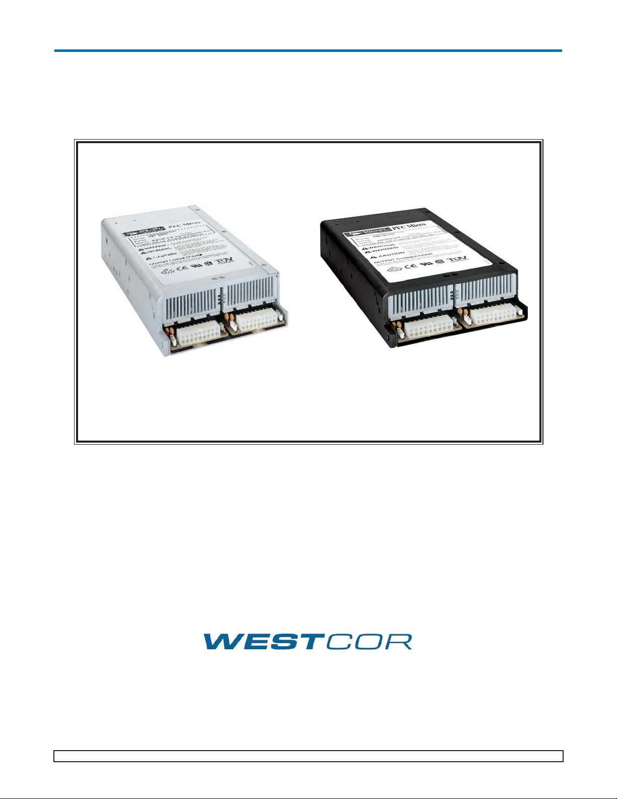
PFC Micro Design Guide
PFC Micro™
Power Factor Corrected AC-DC Switcher
Design Guide
and
“Quick Install” Instructions
www.vicorpower.com
Page 2

Pg. 2 Vicor 800-735-6200 Westcor Division 408-522-5280 Applications Engineering 800-927-9474 03-000048 rev A
PFC Micro Design Guide
TABLE OF CONTENT
Overview of Product...........................................................................................................................3
Part Numbering...................................................................................................................................3
Mechanical Considerations.................................................................................................................4
PFC Micro Do’s and Don't.................................................................................................................4
Technical Description.........................................................................................................................5
Quick Install Instructions....................................................................................................................6
Mechanical Drawings.........................................................................................................................8
Output Connections.............................................................................................................................9
Interface Connections..........................................................................................................................10
Specifications......................................................................................................................................16
Output Power Derating.......................................................................................................................18
Current Share Board...........................................................................................................................20
Page 3

03-000048 rev A Vicor 800-735-6200 Westcor Division 408-522-5280 Applications Engineering 800-927-9474 Pg. 3
PFC Micro™
Power Factor Corrected AC-DC Switcher
Overview
The PFC Micro is an low profile switching power supply that combines the advantages of power factor correction
(PFC) and high power density. This guide covers both standard and rugged COTS (MI) versions of the supply. A
PFC Micro provides up to 6 isolated outputs (from 2 slots) and each slot accommodates the following Vicor DC DC Converters:
VI-200/VI-J00: 2 VI-200 or 4 VI-J00
Maxi/Mini/Micro Series: 2 Maxis, 4 Minis or 6 Micros.
The use of these converters gives the PFC Micro the inherent power flexibility typical of all Vicor products.
Accepting input voltages of 85 Vac to 264 Vac, and 100 to 300 Vdc, the PFC Micro can provide up to 800 Watts in
a package size of 1.86" H (47.3mm) x 5.06" W (128,5mm) x 10.40" L (264,1mm). The PFC Micro is factory configured to meet user output requirements. Using the PowerBench configurator tool available on vicorpower.com,
anybody can now configure a PFC Micro (and other Westcor power supplies) online.
Standard Features
• Power Factor Correction: Typically 0.98 (>75% Load)
• Universal Input: 85-264 Vac, 47-500 Hz, or 120-300 Vdc
• Power Output: 800W at 230 Vac (200 Vac minimum input) ; 500W at 115 Vac (100 Vac minimum input)
• Up to 6 isolated outputs (2 slots)
• Fan cooled
• Full power to 45°C; half power at 65°C
• Soft start for limiting inrush current
• Conducted EMI: FCC Class A; EN 55022 Class A (consult factory)
• Harmonic Distortion to EN61000-3-2
• AC Power OK status signal
• RoHS compliant available
• Output Sequencing and General Shutdown
• Autosense (Refer to page 6 and 11 for more information on Autosense)
• Output overcurrent protection on all outputs
• Output overvoltage protection and output overtemperature limiting (not applicable when using VI-J00)
• Ride-through (holdup) time: >20 ms at 500W load
• Size: 1.86" H (47,3mm) x 5.06" W (128,5mm) x 10.4" L (264,1mm)
• Safety Agency Approvals: CE Marking, TUV CUE (certain models may not have all listed approvals)
• Uses 300 Vdc input VI-200/VI-J00 modules and/or 375 Vdc input Maxi/Mini/Micro modules
• Power good status signal when Maxi, Mini, or Micro modules used
Optional Features
• I/T/H Grade output converters
• Current Share Board for unit to unit power sharing- See page 19 and page 20
• Connector kits (# 19-130044)
• MI Chassis Specific
• Mil-STD 810 for Shock and Vibration
• Mil-STD 704 and 1399 for Overvoltage and transients
• -40C operation
• Conformal coating - contact factory
PFC Micro Design Guide
Page 4

Pg. 4 Vicor 800-735-6200 Westcor Division 408-522-5280 Applications Engineering 800-927-9474 03-000048 rev A
PFC Micro Design Guide
Part Numbering
PFC Micro PCx1-x2 x3 (x4)-xxxx-x
5
x
1
Number of outputs
e.g. PC6-06-5012-G x
2
Number of VI-200/VI-J00 modules
x
3
Number of Maxi, Mini and Micro modules
x
4
Optional Factory assigned
xxxx Sequential number assigned by Westcor
x5 Optional Factory assigned
note: x5 = MI for rugged chassis, =MC for rugged chassis w/conformal coating
Mechanical Considerations
The PFC Micro can be mounted on one of three surfaces using standard 8-32 or 4 mm screws. Maximum allowable
torque is 5 in. lbs., and the maximum penetration of 0.25 in (6mm) on the sides and 0.125 in. (3mm) on the bottom.
When selecting a mounting location and orientation, the unit should be positioned so air flow is not restricted.
Maintain a 2" (5,1cm) minimum clearance at both ends of the PFC Micro, and route all cables so airflow is not
obstructed. The power supply draws air in at the fan side/AC input side and exhausts air out the load side. If airflow ducting is used, avoid sharp turns that could create back pressure. The fan moves approximately 10 CFM of
air.
Avoid excessive bending of output power cables after they are connected to the output terminals. For high-current
outputs, use cable ties to support heavy cables and minimize mechanical stress on connectors. Be careful not to
short-out to neighboring outputs. The maximum torque recommended on output nuts is 10 in. lbs.
Avoid applications in which the unit is exposed to excessive shock or vibration levels as the unit is designed primarily for office type equipment. In such applications, a shock absorbing mount design is required.
PFC Micro Do’s and Don't
• Do not restrict airflow to the unit. The cooling fan draws air into the unit and forces it out at the output power
terminals. A minimum of 2” in front and behind the supply should be maintained in order to prevent air
obstructions.
• Run the output (+/–) power cables next to each other to minimize inductance.
• Do not attempt to repair or modify the power supply in any manner. In the event of problems, contact
Customer Service at 1-800-735-6200..
• Insert proper fault protection at power supply input terminals (i.e., a fuse).
• Use proper size wires to avoid overheating and excessive voltage drop.
• Output voltages over 60Vdc, whether from individual modules or series arrays, are considered as hazardous
secondary outputs under UL 60950. Appropriate care must be taken in design implementation of the supply.
Page 5
03-000048 rev A Vicor 800-735-6200 Westcor Division 408-522-5280 Applications Engineering 800-927-9474 Pg. 5
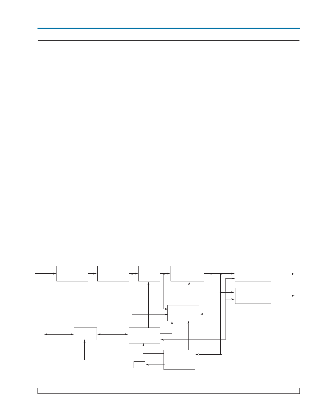
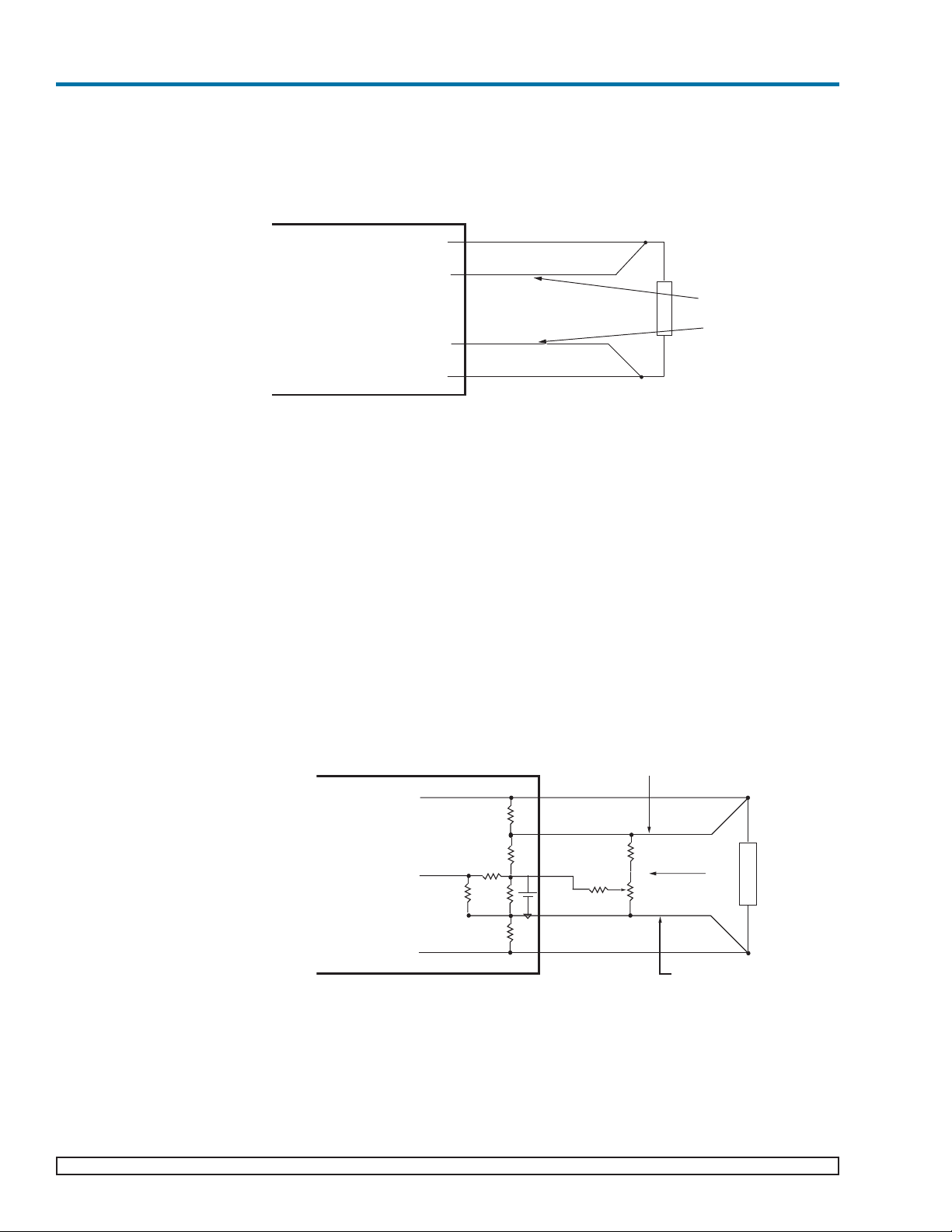
Technical Description
The PFC Micro consists of an off-line single phase, power-factor-corrected front end, EMI filter, cooling fan, customer interface, power supply control circuit, associated housekeeping circuits, and a selection of Vicor’s VI200/VI-J00 and/or Maxi DC-DC converters.
Input AC mains voltage is applied to input connector MB1J1. The input current is passed through an EMI filter
designed to meet conducted noise limit "A" specifications of FCC Part 15.
At start-up, inrush current is limited by a PTC thermistor. The PTC is shunted out shortly after initial power-up by
a DC bus voltage sense circuit driving a relay. After rectification, the input voltage is put through a boost converter
that keeps the AC input current sinusoidal and synchronized with the input AC voltage (in compliance with
EN61000). The boost converter delivers a regulated input to the hold-up capacitors and a high voltage backplane.
The backplane supplies power to the DC-DC converters that provide the desired low voltage regulated outputs.
Output voltage conversion is achieved by Vicor’s family of Zero-Current-Switching (ZCS) DC-DC converters.
These are forward converters in which the main switching element switches at zero current. This patented topology
has a number of unique attributes: low switching losses; high frequency operation, resulting in reduced size for
magnetics and capacitors; excellent line and load regulation; wide adjustment range for output; low EMI/RFI emission and high efficiencies.
At initial power-up, the PFC Micro outputs are disabled to limit the inrush current and to allow the DC bus potential to settle out to the correct operating level. A low-power flyback converter converts the high voltage DC bus
into regulated low voltage to power the internal housekeeping circuits and DC cooling fan.
The internal housekeeping Vcc comes up within 1 s after the application of input power. Once the high voltage bus
is within operating limits, the AC Power OK signal asserts to a TTL "1," indicating the input power is OK, and the
power outputs will come up 250 ms later.
An output Enable/Disable function is provided to control Vicor’s DC-DC converters. If the Enable/Disable control
pin is pulled low, the modules output is disabled. The nominal delay associated for an output to come up when
measured from release of the Enable/Disable pin is 9-12 ms. The General Shutdown function controls all outputs
simultaneously and works in a similar manner.
PFC Micro Design Guide
Figure 1. PFC Micro Architecture
Line Filter
Bridge
Rectifier
Soft Start
Circuit
Boost Converter
PFC Control
Power Supply
Control
Output Card #1
Output Card #2
Fan
Isolated
Housekeeping
Power Supply
Custom
er
Interface
Power
Output
Power
Output
Input
Enable/Disa
ble -Power Good Read
Page 6
Pg. 6 Vicor 800-735-6200 Westcor Division 408-522-5280 Applications Engineering 800-927-9474 03-000048 rev A
PFC Micro Design Guide
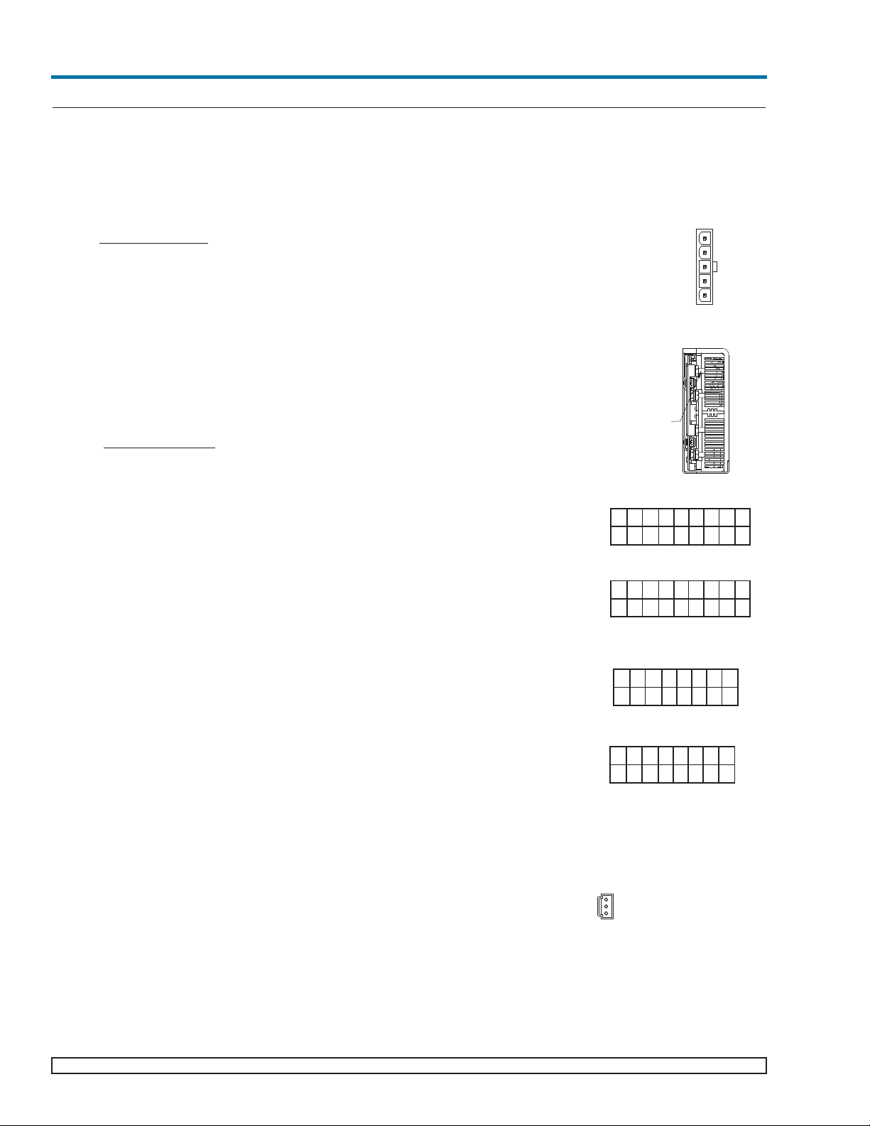
PFC Micro “Quick Install” Instructions (For mechanical drawings, see page 8)
Mounting the PFC Micro
* The PFC Micro can be mounted on either of three sides.
* Use #8-32 or 4mm mounting screws. Maximum penetration should not exceed
0.25in. (6mm) on the side and 0.125 in. (3mm) on the bottom.
* Maintain 2" (5,1cm) clearance at both ends of power supply for airflow.
Input Connections
Input Power MBJ1
* Input AC power is applied to connector MBJ1.
* Maximum torque is 5 in.lbs
* A fuse or circuit breaker in the input line is necessary for safety requirements (10A).
* Molex mating receptacle 39-01-4051, terminals 39-00-0090, crimp tool Molex
# 11-01-0199.
Output Connections
Note: Outputs with current molex connectors are limited to 9A/pin (27A per output). A
PFC Micro with DIFFERENT Molex connectors capable of 40A is available. Contact
factory.
Power Connections
Installing bus bars on output studs (when full size module used):
* The right stud is Positive and the left stud is the Return on single output cards.
* Remove the nut and place ring lug over output stud.
* Replace and tighten the nut to a torque of 10 inch pounds.
Do Not Over-Tighten Nuts.
Installing power connectors with 18 pin Molex connectors (when half size mod-
ules used):
* S1/S2 J1-7, S1/S2 J1-8 and S1/S2 J1-16 are Positive for output #1, while pins
S1/S2 J1-9, S1/S2 J1-17 and S1/S2 J1-18 are the Returns. S1/S2 J1-1, S1/S2
J1-10 and S1/S2 J1-11 are Positive for output #2, while pins S1/S2 J1-2, S1/S2
J1-3 and S1/S2 J1- 12 are the Returns.
* For this 18 pin housing, use Molex mating receptacle #39-01-2180 with #39-
00-0039 terminals.
* Attach 18-24 AWG stranded wire using Molex tool #11-01-0197.
Installing power connectors with 16 pin Molex connectors (when quarter size
modules used):
* S1/S2 J1-7 and S1/S2 J1- 15 are Positive for output #1, while pins S1/S2 J1-8
and S1/S2 J1- 16 are the Return. S1/S2 J1-4 and S1/S2 J1-12 are Positive for
output #2, while pins S1/S2 J1-5 and S1/S2 J1- 13 are the Return. S1/S2 J1-1
and S1/S2 J1-9 are Positive for output # 3, while pins S1/S2 J1-2, and S1/S2
J1-10 are the Returns.
* For this 16 pin housing, use Molex mating receptacle #39-01-2160 with #39-
00-0039 terminals.
* Attach 18-24 AWG stranded wire using Molex tool #11-01-0197.
Sense Connections
Sense Connections on output connections with studs:
* The PFC Micro is shipped with Autosense installed (For more information on
Autosense, refer to page 12)
* For Remote Sense, connect Remote Sense wires to Remote Sense/Trim Pin
Access Connector S1/S2 J2.
* Connector pin S1/S2 J2-2 is the +Sense and S1/S2 J2-3 is the -Sense.
* Use Molex mating receptacle #50-57-9403 with #16-02-0103 terminals.
MBJ1-5 PIN
Not Connected
GND
L2/N
L1
Not Connected
1
2
3
Sense Connections
Trim Pin
+ Remote Sense
- Remote Sense
Pin
S1/S2 J2
- + + T - + - - +
- - + - T + - + +
S1/S2 J1 (18 Pin)
10-32 STUDS
S1/S2 J1
18 17 16 15 14 13 12 11 10
9 8 7 6 5 4 3 2 1
S1/S2J1
16 15 14 13 12 11 10 9
8 7 6 5 4 3 2 1
MAXI MODULE
(2 ISOLATED OUTPUTS)
-
S1
+
-
S2
+
S1/S2J1 (16 Pin)
- + T - +
- + T - + T - +
N/C - +
Page 7
03-000048 rev A Vicor 800-735-6200 Westcor Division 408-522-5280 Applications Engineering 800-927-9474 Pg. 7
PFC Micro Design Guide
* Attach terminals to 24-30 AWG stranded twisted pair wire using Molex tool #
11-01-0208.
* Attach opposite end of sense lines to their respective outputs to point where
regulation is desired. Verify that sense lines are not cross-connected.
Sense Connections on output connections with 18 pin Molex connectors:
* The PFC Micro is shipped with Autosense installed (For more information on
Autosense, refer to page 11)
* If Remote Sense is desired, connect Remote Sense wires to sense lines of
Connector S1/S2 J1.
* Connector pin S1/S2 J1- 13 is the +Sense and S1/S2 J1- 15 is the -Sense for
output #1. S1/S2 J1- 4 is the +Sense and S1/S2 J1- 5 is the -Sense for output
#2.
* Use Molex mating receptacle #39-01-2180 with #39-00-0039 terminals.
* Attach 18-24 AWG stranded twisted pair wire using Molex tool #11-01-0197
Note: Remote Sense is NOT available for triple output slots.
Trim Connections
Trim Connections on output with studs :
* S1/S2 J2-1 provides Trim access.
* Use Molex mating receptacle #50-57-9403 with #16-02-0103 terminals.
* Attach 18-24 AWG stranded wire using Molex tool #11-01-0208.
Trim Connections on connector with 18 pin molex connectors:
* S1/S2 J1-6 provides Trim access for output #1, and S1/S2 J1-14 provides Trim
access for output #2.
* Use Molex mating receptacle #39-01-2180 with #39-00-0039 terminals.
* Attach 18-24 AWG stranded wire using Molex tool #11-01-0197.
Trim Connections on connectors with 16 pin Molex connectors:
* S1/S2 J1-14 provides Trim access for output #1, and S1/S2 J1-6 provides Trim
access for output #2, and S1/S2 J1-3 provides Trim access for output #3.
* Use Molex mating receptacle #39-01-2180 with #39-00-0039 terminals.
* Attach 18-24 AWG stranded wire using Molex tool #11-01-0197.
Interface Connections
* CBJ3-1 is Signal Ground, CBJ3-2 is Power Good Read and CBJ3-3 is
AC-OK.
* CBJ3-4-9 are Enable/Disable,CBJ3-10 is General Shutdown, CBJ3-11 is
Power Good Data Valid (PGDV) and CBJ3-12 is +5VS.
* Use Molex mating receptacle #50-57-9412 with #16-02-0097 cinch pins.
* Attach terminals to 24-30 AWG stranded wire.
1
2
3
Trim Connectio
ns
Trim Pin Access
+ Sense
- Sense
P
in
S1/S2 J2
CBJ3 E/D INTERFACE CONNECTOR
MATING CONNECTOR: (WESTCOR KIT P/N: 19-130044)
HOUSING: MOLEX (50-57-9412)
SOCKET CRIMP 24-30 AWG: MOLEX (16-02-0097)
CRIMP TOOL: MOLEX (11-01-0209)
PIN DESCRIPTION
CBJ3-1 SGND
CBJ3-2 PGR
CBJ3-3 ACOK
CBJ3-4 ED6
CBJ3-5 ED5
CBJ3-6 ED4
CBJ3-7 ED3
CB3-8 ED2
CBJ3-9 ED1
CBJ3-10 GSD
CBJ3-11 PGDV
CBJ3-12 +5 VS
9 8 7 6 5 4 3 2 1
18 17 16 15 14 13 12 11 10
S1/S2 J1
- + + T - + - - +
- - + - T + - + +
S1/S2 J1 (18 Pin)
- + + T - + - - +
- - + - T + - + +
S1/S2 J1 (18 Pin)
S1/S2 J1
18 17 16 15 14 13 12 11 10
9 8 7 6 5 4 3 2 1
S1/S2J1
16 15 14 13 12 11 10 9
8 7 6 5 4 3 2 1
S1/S2J1 (16 Pin)
- + T - +
- + T - + T - +
N/C - +
Page 8
Pg. 8 Vicor 800-735-6200 Westcor Division 408-522-5280 Applications Engineering 800-927-9474 03-000048 rev A
PFC Micro Design Guide
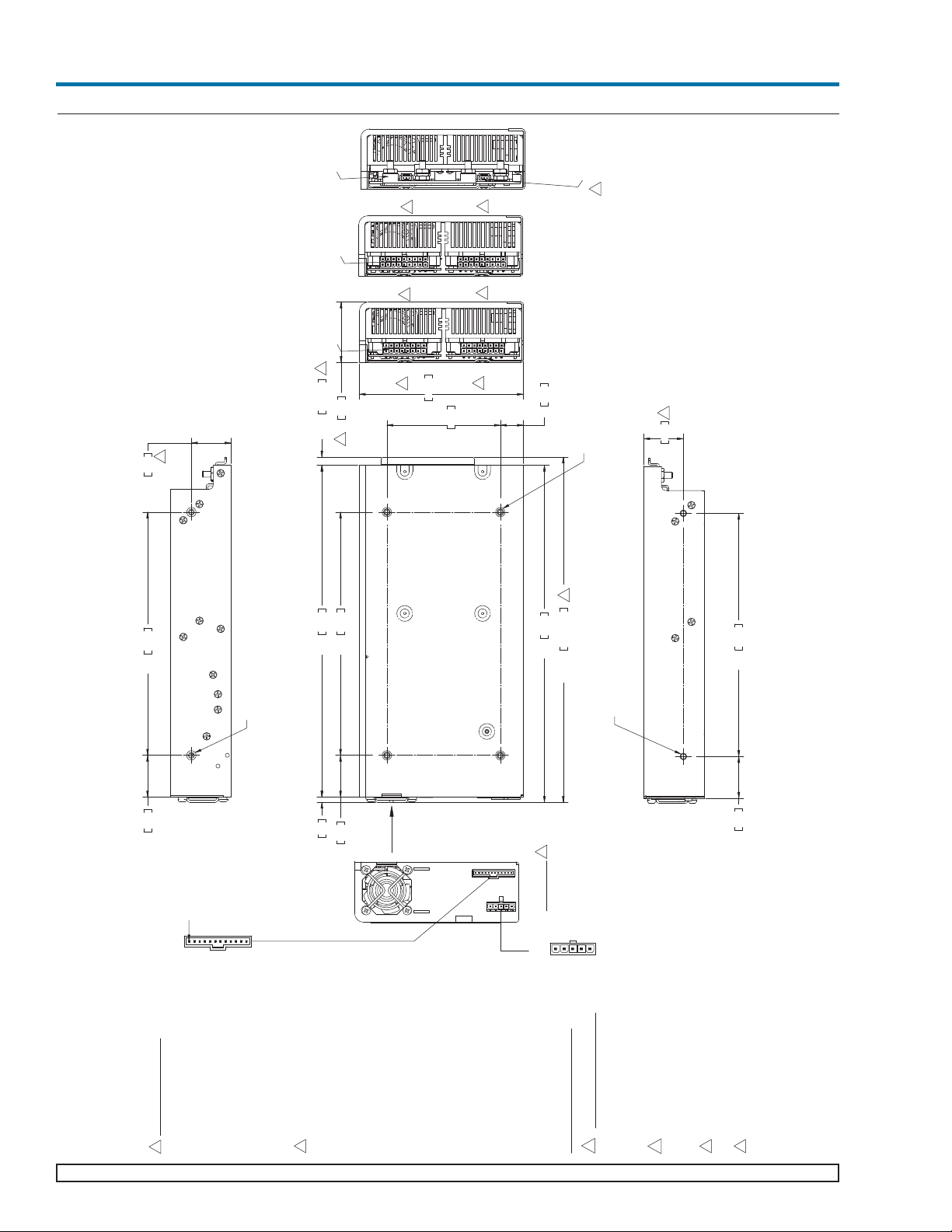
PFC Micro Mechanical Drawings
NOTES: UNLESS OTHERWISE SPECIFIED
2
32.691.29 190.507.500
31.041.22
MOUNTING HOLES; 2 PLACES
USE 8-32 X 0.25 or M4 X 6MM MAX LENGTH
FROM OUTSIDE OF UNIT
32.691.29 190.507.500
264.1110.40 18.03.71
88.903.500
6.35±0.51.25±.024.09.16 260.0210.24
270.46±0.5110.65±.02
MOUNTING HOLES; 4 PLACES
USE 8-32 X 0.12 or M4 X 3MM MAX LENGTH
FROM OUTSIDE OF UNIT
3
3
4
31.041.22190.507.50032.691.29
MOUNTING HOLES; 2 PLACES
USE 8-32 X 0.25 or M4 X 6MM MAX LENGTH
FROM OUTSIDE OF UNIT
4
3
2
PIN-1
4
1
L1
L2/N
GND
N/C
N/C
4
128.525.06
47.291.86
S1
S2
MBJ1 (5 PIN)
MBJ1 A/C INPUT
MATING CONNECTOR:
HOUSING: MOLEX (39-01-4051)
TERMINAL: MOLEX (39-00-0090)
CRIMP TOOL: MOLEX (11-01-0199)
CBJ3 INTERFACE CONNECTOR
MATING CONNECTOR:
HOUSING: MOLEX (50-57-9412)
SOCKET CRIMP 24-30 AWG: MOLEX (16-02-0097)
CRIMP TOOL: MOLEX (11-01-0209)
CBJ3 (12 PIN)
PIN REF DESCRIPTION
CBJ3-1 SGND SIGNAL GROUND
CBJ3-2 PGR POWER GOOD/READ
CBJ3-3 ACOK AC POWER OK
CBJ3-4 ED6 ENABLE/DISABLE S2M3
CBJ3-5 ED5 ENABLE/DISABLE S2M2
CBJ3-6 ED4 ENABLE/DISABLE S2M1
CBJ3-7 ED3 ENABLE/DISABLE S1M3
CBJ3-8 ED2 ENABLE/DISABLE S1M2
CBJ3-9 ED1 ENABLE/DISABLE S1M1
CBJ3-10 GSD GENERAL SHUTDOWN
CBJ3-11 PGDV POWER GOOD/DATA VALID
CBJ3-12 Vcc +5V@40mA
PFC MICRO
AIR
FLOW
WITH OPTIONAL BUS BAR
1
1
A COMPLETE SET OF MATING CONNECTORS
IS AVAILABLE FOR PURCHASE BY SPECIFYING
WESTCOR CONNECTOR KIT P/N: 19-130044.
1
2
REFERENCE DESIGNATIONS
MB MOTHER BOARD
CB CONTROL BOARD
S(x) SLOT NUMBER
M(x) MODULE NUMBER
DUAL OUTPUT UNIT
PICTURED (TWO
MAXI
MODULES)
QUAD OUTPUT
UNIT PICTURED
(FOUR MINI
MODULES)
-
+
-
+
10-32 STUDS
S1
S1
S2
S2
18 PIN CONNECTOR
S1/S2 J2 REMOTE SENS
ACCESS CONNECTOR
1
SEE PAGE 9 FOR DETAILED OUTPUT
CONNECTION INFORMATION .
16 PIN CONNECTOR
SIX OUTPUT UNIT
PICTURED (THREE
MICRO
MODULES)
1
1
1
1
NOTE: FOR INCREASED OUTPUT POWER, CURRENT SHARE BOARDS ARE
AVAILABLE.
WITH VI-200/VI-J00 MODULES CSB-01
WITH MAXI/MINI/MICRO MODULES CSB-02
(SEE PAGE 19 AND 20 FOR MORE INFORMATION ON CURRENT SHARE
BOARDS.
DIMENSIONS SHOWN ARE FROM BOTTOM SURFACE
MOUNTING PEMNUTS EXTEND .010 PAST BOTTOM
SURFACE.
All Westcor power supplies can now be configured online
using VSPOC, the online configurator tool available on vicorpower.com
Page 9

03-000048 rev A Vicor 800-735-6200 Westcor Division 408-522-5280 Applications Engineering 800-927-9474 Pg. 9
2
3
4
5
6
7
8
11
12
13
14
15
16
17
1
10
9
18
1 +V OUT M2
2 -V OUT M2
3 -V OUT M2
4 + SENSE M2
5 - SENSE M2
6 TRIM M1
7 +V OUT M1
8 +V OUT M1
9 -V OUT M1
10 +V OUT M2
11 +V OUT M2
12 -V OUT M2
13 + SENSE M1
14 TRIM M2
15 - SENSE M1
16 +V OUT M1
17 - V OUT M1
18 - V OUT M1
MATING CONNECTOR:
18 PIN HOUSING: MOLEX (39-01-2180)
TERMINAL FEM CRIMP 18-24 AWG: MOLEX (39-00-0039)
USE CRIMP TOOL: MOLEX (11-01-0197)
PIN DESCRIPTION PIN DESCRIPTION
10-32 OUTPUT STUDS
- SENSE
3
SxJ2 REMOTE SENSE/TRIM
PIN CONNECTOR
1
2
TRIM
+ SENSE
MATING CONNECTOR:
HOUSING: MOLEX (50-57-9403)
TERMINAL FEM CRIMP 24-30 AWG: MOLEX (16-02-0103)
USE CRIMP TOOL: MOLEX (11-01-0208)
B. 18 PIN MOLEX CONNECTOR - SINGLE OR DUAL OUTPUTS (when populated with half size modules)
A. OUTPUT STUDS - SINGLE OUTPUT (when populated with full size module)
SxJ1 (18 PIN OUTPUT, REMOTE SENSE
AND TRIM PIN CONNECTOR)
-V OUT
+V OUT
2
3
4
5
6
7
8
10
11
12
13
14
15
16
1
9
MATING CONNECTOR:
16 PIN HOUSING: MOLEX (39-01-2160)
TERMINAL FEM CRIMP 18-24 AWG: MOLEX (39-00-0039)
USE CRIMP TOOL: MOLEX (11-01-0197)
9 +V OUT M3
10 -V OUT M3
11 N/C
12 +V OUT M2
13 -V OUT M2
14 TRIM M1
15 +V OUT M1
16 -V OUT M1
1 +V OUT M3
2 -V OUT M3
3 TRIM M3
4 +V OUT M2
5 -V OUT M2
6 TRIM M2
7 +V OUT M1
8 -V OUT M1
*SxJ1 (16 PIN OUTPUT, REMOTE SENSE
AND TRIM PIN CONNECTOR)
PIN DESCRIPTION PIN DESCRIPTION
C. 16 PIN MOLEX CONNECTOR - SINGLE, DUAL, TRIPLE OUTPUTS (when populated with quarter size modules)
Note: The current molex connectors are limited
to 9A/pin (27A per output). A PFC Micro with
DIFFERENT molex connectors that are capable
of 40A is available. Contact factory!
PFC Micro Design Guide
Output Connections for the PFC Micro
OPTIONAL CONNECTOR KIT FOR PFC MICRO (PART# 19-130044. Available for purchase from Westcor)
Page 10

Pg. 10 Vicor 800-735-6200 Westcor Division 408-522-5280 Applications Engineering 800-927-9474 03-000048 rev A
PFC Micro Design Guide
Interface Connections
Chassis Input Power Terminals (MBJ1)
Input AC power is applied through connector MBJ1 using Molex mating connector 39-01-4051. Use 16 AWG
wire with Molex Socket Pin 39-00-0090 and Crimp Tool 11-01-0199.
A fault clearing device, such as a fuse or circuit breaker, with a maximum 10A rating at the power supply input is
required for safety agency compliance. It should be sized to handle the start-up inrush current of 8.5A peak at 115
Vac and 17A peak at 230 Vac.
Output Power Connections
There are three types of output power terminals available in the PFC Micro. Each slot has one of the following
configurations: 10-32 plated steel bolts from outputs using full size converters, an 18 pin Molex connector for outputs using half size converters and a 16 pin Molex connector for outputs using quarter size converters. Note: The
Molex connectors are limited to 9A/pin (27A/output)). The positive polarity of the single output termination is the
right bolt when viewed from the output end. Each power output is isolated, so outputs of positive or negative
polarity can be configured through proper selection of the output reference terminal.
In order to minimize parasitic cable inductance and reduce EMI, the output power cables should be routed in close
proximity to one another, and large current loops should be avoided. To avoid excessive voltage drop, do not
undersize power cables, especially for high current outputs. Do not bulk input AC wires with the output wires
because this can couple output noise into the input wires which can increase EMI. Excessive cable inductance
coupled with large capacitive loading can introduce instability in switching power supplies. This problem can be
avoided with proper system design. Consult Vicor’s Applications Engineering Department for assistance with
applications that use long cable lengths and excessive load capacitance.
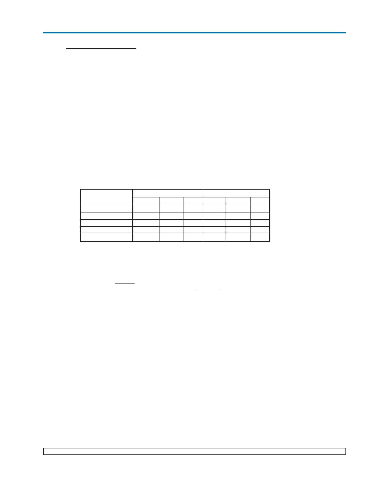
Figure 2. Input Power Terminal MBJ1
S1/S2 J1 REMOTE SENSE/OUTPUT CONNECTORS
MATING CONNECTORS: (WESTCOR KIT P/N: 19-130044)
16 PIN HOUSING: MOLEX (39-01-2160)
SOCKET CRIMP 18-24 AWG: MOLEX (39-00-0039)
CRIMP TOOL: MOLEX (11-01-0197)
PIN DESCRIPTION
S1/S2 J1-9 +V OUT M3
S1/S2 J1-10 -V OUT M3
S1/S2 J1-11 N/C
S1/S2 J1-12 +V OUT M2
S1/S2 J1-13 -V OUT M2
S1/S2 J1-14 TRIM M1
S1/S2 J1-15 +V OUT M1
S1/S2 J1-16 -V OUT M1
PIN DESCRIPTION
S1/S2 J1-1 +V OUT M3
S1/S2 J12 -V OUT M3
S1/S2 J1-3 TRIM M3
S1/S2 J1- 4 +V OUT M2
S1/S2 J1-5 -V OUT M2
S1/S2 J1-6 TRIM M2
S1/S2 J1- 7 +V OUT M1
S1/S2 J1-8 -V OUT M1
S1/S2 J1 (16 PIN, TRIPLE MICRO MODULES)
PIN DESCRIPTION
S1/S2 J1- 1 +V OUT M2
S1/S2 J1-2 -V OUT M2
S1/S2 J1-3 -V OUT M2
S1/S2 J14 + SENSE M2
S1/S2 J15 - SENSE M2
S1/S2 J16 TRIM M1
S1/S2 J17 +V OUT M1
S1/S2 J1 8 +V OUT M1
S1/S2 J19 -V OUT M1
PIN DESCRIPTION
S1/S2 J110 +V OUT M2
S1/S2 J111 +V OUT M2
S1/S2 J1 12 -V OUT M2
S1/S2 J113 + SENSE M1
S1/S2 J114 TRIM M2
S1/S2 J115 - SENSE M1
S1/S2 J116 +V OUT M1
S1/S2 J117 - OUT M1
S1/S2 J118 - OUT M1
S1/S2 J1 (18 PIN, DUAL MINI & VI-J00 MODULES)
TRIPLE MICRO
MODULES (6 OUTPUTS)
MAXI MODULE
(2 ISOLATED OUTPUTS)
DUAL MINI
MODULES (4 OUTPUTS)
-
+
-
+
S1
S2
S1
S1
S1
S2
10-32 STUDS
128.525.06
47.291.86
Trim Pin
3
2
1
S1/S2 J2 REMOTE SENSE/TRIM PIN ACCESS CONNECTOR
MATING CONNECTOR: (WESTCOR KIT P/N: 19-130044)
HOUSING: MOLEX (50-57-9403)
SOCKET CRIMP 24-30 AWG: MOLEX (16-02-0103)
CRIMP TOOL: MOLEX (11-01-0208)
+ REMOTE SENSE
S1/S2 J2-3 PIN (VI-200/MAXI MODULE)
9 8 7 6 5 4 3 2 1
18 17 16 15 14 13 12 11 10
8 7 6 5 4 3 2 1
16 15 14 13 12 11 10 9
S1/S2 J1 REMOTE SENSE/OUTPUT CONNECTORS
MATING CONNECTORS: (WESTCOR KIT P/N: 19-130044)
18 PIN HOUSING: MOLEX (39-01-2180)
SOCKET CRIMP 18-24 AWG: MOLEX (39-00-0039)
CRIMP TOOL: MOLEX (11-01-0197)
- REMOTE SENSE
Note: The molex connectors are limited
to 9A/pin (27A per output)
Figure 3. Output Power Connections
CBJ3-12 PIN
PIN 1
MBJ1 A/C INPUT
MATING CONNECTOR: (WESTCOR KIT P/N: 19-130044)
HOUSING: MOLEX (39-01-4051)
SOCKET CRIMP 16 AWG: MOLEX (39-00-0090)
CRIMP TOOL: MOLEX (11-01-0199)
Not Connected
MBJ1 (5 PIN)
Not Connected
L1
L2/N
GND
Page 11
03-000048 rev A Vicor 800-735-6200 Westcor Division 408-522-5280 Applications Engineering 800-927-9474 Pg. 11
PFC Micro Design Guide
User Interface Connections
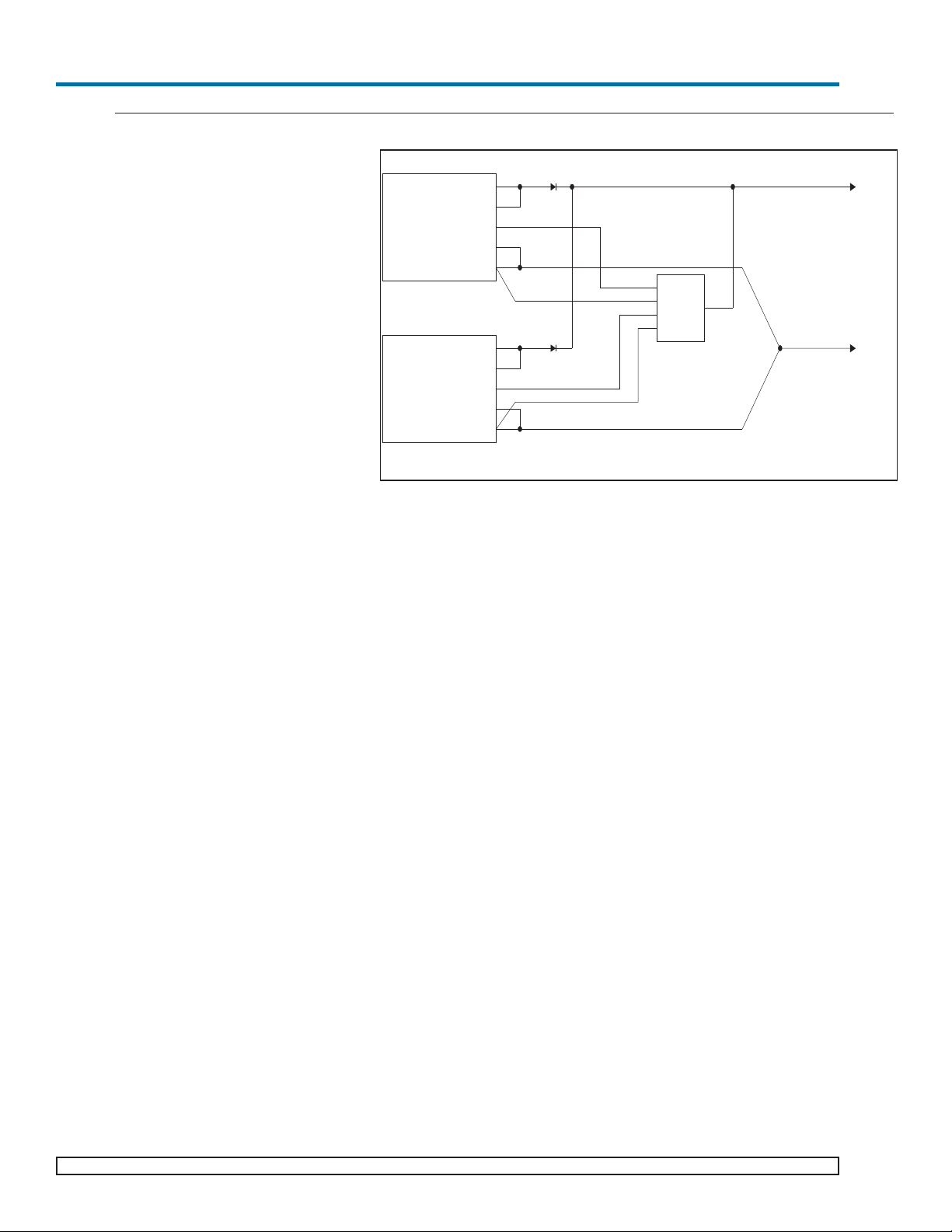
Signal Ground (CBJ3-1)
Signal Ground on CBJ3-1 is an isolated secondary ground reference for all CBJ3 interfacing signals. This is not
the same as Earth Ground on input power connector MBJ1.
Bi -directional I/O lines (CBJ3-4 to CBJ3-9) (Enable/Disable or Module Power Good Status)
Enable/Disable Mode
Enable/Disable mode is the default condition for these I/O lines. In this mode, the control pins allow the outputs
to be sequenced either ON or OFF. To disable a module, the E/D pin should be pulled low to less than 0.7V with
respect to Signal Ground. The E/D lines will typically source 250μA (1mA max.) under this condition. To enable
a module, a E/D pin should be open circuited or driven high to a logic high voltage of 3.5V (40μA typical) or
greater not to exceed 5V. (When one has a two module array, use GSD to disable the output instead of using E/D.)
The correspondence between a module and its E/D line as seen from the output end of the power supply goes from
left to right. The PFC Micro Power Supply is a two slot box. Slot 1 is the left slot and Slot 2 is the right slot. See
Table 1. E/D1, E/D2, E/D3 correspond with V
out
M1, V
out
M2 and V
out
M3 on slot 1. E/D4, E/D5, E/D6 cor-
respond with V
out
M1, V
out
M2 and V
out
M3 on slot 2.
Table 1: Enable/Disable Mode
Module Power Good Status Mode
The power supply will enter the Power Good Status Mode when logic high (50mA typical) is applied to Power
Good Read (PGR) pin (CBJ3-2). After transitioning to PGR mode the I/O lines (CBJ3-4 to CBJ3-9) will be outputs and will give a onetime
readout of the associated module status.. These outputs give an indication of the status of the modules of the power supply at the time of transition to PGR. A TTL "1" (>3.5V) on a line indicates the
module is ON and functioning properly, and a TTL "0" (<0.7V) indicates the module is either OFF or is not functioning properly. The correspondence between the module and the Power Good Status of that module is the same
as between a E/D pin and its module. This mode does NOT constantly monitor the module status and must be retriggered by transitioning the PGR pin from logic low to logic high to get current module status
Procedurally, certain guidelines must be followed when using this feature. Upon application of a logic high on the
Power Good Read (PGR) pin, the user must change its E/D interface (CBJ3-4 to CBJ3-9) from outputs to inputs
within 3 ms. The Power Good Status data will be valid on the E/D lines when the Power Good Data Valid (PGDV)
pin (CBJ3-11) asserts to a logic high. The power good status measurement takes typically 200ms. While in the
Power Good Read Mode (PGR=1) the individual shutdown lines are not functional. However, General Shut Down
(GSD) is functional. Leaving the Power Good Read mode is accomplished by removing the logic high or applying
a logic low (<0.7V) to the Power Good Read (PGR) pin (CBJ3-2). The user must change its E/D interface (CBJ34 to CBJ3-9) from inputs to outputs between 1ms and 4ms of the time the PGR low is applied to pin CBJ3-2.
Note: If any model is disabled by the user when a Power Good Read is requested (PGR=1), that module will
remain off during the Power Good Read and status of said module will be power not good (<0.7V). Power Good
Read status data on open E/D lines are not valid. An open E/D line is a E/D pin where there is no module associated with said E/D line (i.e. A power supply with two Maxi modules, Data on E/D2, E/D3 and E/D5 and E/D6 are
NOT valid.
The Power Good Status Mode feature is only valid when Maxi, Mini and/or Micro modules are used.
The following page shows examples of triggering PGR with a 1Hz square while monitoring PGDV and a selected
E/D line with a good module and a defective one
Slot 1 Slot 2
E/D1 E/D2 E/D3 E/D4 E/D5 E/D6
Maxi Modules X X
Mini Modules X X X X
Micro Modules XXXXXX
VI-200 Modules X X
VI-J00 Modules X X X X
Page 12

PFC Micro Design Guide
PowerGood Read with Good Module
PowerGood Read with Defective Module
Pg. 12 Vicor 800-735-6200 Westcor Division 408-522-5280 Applications Engineering 800-927-9474 03-000048 rev A
Page 13

PFC Micro Design Guide
General Shutdown /GSD (CBJ3-10)
The GSD control pin on CBJ3-10 allows simultaneous shutdown of all outputs. This pin must be pulled down to
less than 0.7V, and will typically source 250μA (1mA maximum) to shut down all outputs. The GSD pin should be
open circuited or driven high to a logic high voltage of 3.5V or greater when not in use, or when the outputs are to
be enabled. Do not apply more than 5V to this input.
AC OK (CBJ3-3)
AC OK is an active high TTL compatible signal and provides a status indication of the AC input power. It is on pin
CBJ3-3 and is capable of sinking 5 mA maximum. This signal switches to a TTL "1" when the high voltage bus
exceeds low-line condition during turn-on. Upon loss of input power, the bus voltage will drop, causing the AC OK
signal to go low. Typically, a 3 ms holdup time is provided for a 500W load following the loss of the AC OK signal.
Auxiliary Vcc +5V/40mA (CBJ3-12)
The Vcc on CBJ3-12 is an auxiliary 5V regulated power source. It is +5 Vdc +/–5% with respect to Signal Ground
and can supply 40 mA maximum. It is capable of withstanding a short, but shorted user interface functionality will
be lost.
Power Good Read (PGR, CBJ3-2)
This pin initiates the Power Good Read sequence. A logic high applied to this pin will cause the power supply to
enter the Power Good Read status mode. In this mode, the I/O lines (CBJ3-4 to CBJ3-9) will be outputs. These
outputs give an indication of the status of the modules of the power supply. A high on an I/O line (CBJ3-4 to
CBJ3-9) indicates a module is ON and functioning and a low indicate the module is OFF or in a fault condition.
The Power Good Status data will be valid on the ED lines (CBJ3-4 to CBJ3-9) when the Power Good Data Valid
(PGDV) pin (CBJ3-11) asserts a logic high. Applying a logic low or opening the PGR pin puts the power supply
back in the Enable/Disable mode. Instructions for using this function are on page 11 under Module Power Good
Status Mode
Power Good Data Valid (PGDV- CBJ3-11)
Upon entering the Power Good Read status mode (PGR=1, CBJ3-2), the data will not be valid on the I/O lines
(CBJ3-4 to CBJ3-9) until the PGDV pin asserts itself logic high. This pin can source up to 5mA. When this pin is
logic low, Power Good status data is not valid or the power supply is not in the Power Good Read status mode.
+Sense/ –Sense (S1/S2 J2)
The sense lines for the outputs are shipped from the factory with Autosense. Autosense provides the user with
automatic sensing of the outputs. With Autosense, the PFC Micro will automatically operate in a Remote Sense
mode when the Remote Sense connections are made. But in the event that the Remote Sense is not connected or
needed, no Local Sense selection is necessary - simply hook up the outputs and the PFC Micro will automatically
operate in Local Sense mode.
In the local sense mode (Remote Sense lines not connected), the power supply will regulate the output at the output
terminals. The voltage appearing at the load may drop slightly due to voltage drop in the power cables. If it is necessary to compensate for voltage drop along the output power cables, the output can be trimmed up or configured
for Remote Sense. Use stranded twisted pair 20-22 AWG wire for the Remote Sense lines. Remote Sense can compensate for a voltage drop of up to 0.5V, or 0.25V on each leg.
Figure 4. Auxiliary Vcc
03-000048 rev A Vicor 800-735-6200 Westcor Division 408-522-5280 Applications Engineering 800-927-9474 Pg. 13
CBJ3
78M05
+5V/40 mA
0.1 µF
CBJ3-12
CBJ3-1
Auxiliary Vcc
Signal Ground
Page 14
PFC Micro Design Guide
The Sense connector for a single output board is a 3 pin connector providing the +Sense connection on S1/S2 J2-2
and the -Sense connection on S1/S2 J2-3. The Sense connector for a dual output board is provided on the 18 pin
output connector that also provides the output and trim connections. +Sense and -Sense for the first output are
located on S1/S2 J1-13 and S1/S2 J1-15, respectively. +Sense and -Sense for the second output are located on
S1/S2 J1-4 and S1/S2 J1-5, respectively. Remote sense is not available for Triple output configurations.
External Trim (S1/S2 J2)
The Trim pin at S1/S2 J2 is referenced to the -Sense pin and can be used for external control of the output voltage. For triple output cards, the Trim pins are available on S1/S2 J2-14, S1/S2 J2-6 and S1/S2 J2-3 for outputs 1,
2 and 3 respectively. For dual output cards, the Trim pins are available at S1/S2 J2-6 and S1/S2 J2-14 for outputs
1 and 2, respectively. For a single output card , the Trim pin is S1/S2 J2-1. A 10% increase to the trim pin voltage will result in a 10% increase in output voltage. Reducing the trim pin voltage by 10% will result in a 10%
decrease in output voltage.
OUTPUT MODULE V
ref
R
TH
VI-200/VI-J00 ≥3.3V 2.5V 10kΩ
VI-200/VI-J00 <3.3V 0.97V 3.88kΩ
Maxi (Predefined) 1.23V 1kΩ
Maxi (Userdefined) 1.23V Consult Factory
Table 2. Module Internal Reference Voltages and Thevenin Resistances.
Figure 5. Remote Sense
(Remote Sense)
Load
+P +Out
S1/S2 J2-2 +Sense
S1/S2 J2-3 -Sense
-P -Out
Use 20-22 AWG Twisted Pair Wires
2.5V
Ref.
S1/S2 J2-1
R6
R8
R7
To Error
Amplifier
+
V
2
-
Use 20-22 AWG Twisted Pair Wires
Figure 6. External Trim
Pg. 14 Vicor 800-735-6200 Westcor Division 408-522-5280 Applications Engineering 800-927-9474 03-000048 rev A
+Out
+Sense
Load
-Sense
-Out
Use 20-22 AWG
Twisted Pair Wires
Page 15

PFC Micro Design Guide
Example:
±10% trim adjust on a 12V nominal output.
Figure 6 shows a typical variable trim circuit. Using a 10k trimpot (R7), the resistor values for R6 and R8 can be calculated as follows:
V
1
= V
ref
+ 10% = 2.75V Given: V
ref
= 2.5V (see Table 2)
I
R5
= (2.75V - V
ref
)/RTH= (2.75V - 2.5V)/10kΩ = 25μA Given: RTH= 10kΩ (see Table 2)
Setting the bottom limit:
V
R6
= 2.5V - 10% = 2.25V
And since I
R5
= IR6= 25μA,
R6 = V
R6/IR6
= 2.25V/25μA = 90kΩ
V2= V1+ VR6= 2.75V + 2.25V = 5V
I
R7
= V2/R7 = 5V/10kΩ = 500μA
I
R8
= IR7+ IR6= 525μA
V
R8
= (V
nom
+10%) - V2= 13.2V - 5V = 8.2V Given: V
nom
= 12V
R8 = V
R8/IR8
= 8.2V/525μA = 15.62kΩ
Consult Applications Engineering when trimming outputs below 5V.
Single Output Power Supplies (Arrays)
Westcor’s standard configuration for single output power supplies is to set the left module (as seen from looking
at the power supply output) as the controlling module of the array.
03-000048 rev A Vicor 800-735-6200 Westcor Division 408-522-5280 Applications Engineering 800-927-9474 Pg. 15
Page 16

PFC Micro Design Guide
Specifications (Typical at 25°C, nominal line and 75% load, unless otherwise specified)
GENERAL
Number of Outputs 1-6
Modules VI/E-200 and VI/E-J00: Two VI/E-200s or Four V/EI-J00s
Maxi: Two Maxis, Four Minis or Six Micros
Efficiency Typically > 75%
Safety Agency Approvals cURus – UL 60950-1, CSA 60950-1;
cTUVus – EN 60950-1, UL 60950-1, CSA 60950-1
CE Mark – Low Voltage Directive, 2006/95/EC
Note: certain wide temp range MI chassis will not carry all approvals
Maximum Output Power 500W at 115Vac, (100 Vac minimum input)
+
800W at 230Vac, (200 Vac minimum input)
+
Note; Not to exceed an input current of 7.5A.
INPUT
Input 85-264 Vac, 47-500Hz
120-300 Vdc (derated output level)
VI-200/VI-J00 Line/Load Regulation 0.2% max. from 10% to full load
0.5% max. from no load to 10% load
Maxi/Mini/Micro Line Regulation* 0.20% max to 0.30%max
Maxi/Mini/Micro Load Regulation* 0.20% max to 0.70% max
Inrush Current 8.5A peak @ 115 Vac
17A peak @ 230 Vac
Ride Through Time >20 ms at 500W load (nominal load)
Conducted EMI FCC Class A
EN 55022 Class A (consult factory)
Mil-STD 461 requires external filter
Power Factor >.98
Transient Burst Immunity EN61000-4-4 (consult factory)
Surge Immunity Compliant with IEC 61000-4-5, Level 3, Performance Criteria B
(Common Mode & Normal Mode) (Temporary loss of output power may occur which is self recoverable.)
Dielectric Withstand Primary to Chassis GND = 2,121 Vdc
Secondary to Chassis GND = 750 Vdc
MI Chassis Overvoltage and Transients Compliant to Mil-STD 704 and 1399
* See Vicor module specifications. A preload may be necessary for modules trimmed down below 90% of normal
output voltage.
Pg. 16 Vicor 800-735-6200 Westcor Division 408-522-5280 Applications Engineering 800-927-9474 03-000048 rev A
Page 17

PFC Micro Design Guide
03-000048 rev A Vicor 800-735-6200 Westcor Division 408-522-5280 Applications Engineering 800-927-9474 Pg. 17
OUTPUT
VI-200/VI-J00 Modules
Parameter MIN. TYP. MAX. UNITS NOTES
Setpoint Accuracy* 0.5 1 % of Vnom
Load/line Regulation 0.05 0.5 % LL to HL, 10% to Full Load
Load/line Regulation 0.2 0.5 % LL to HL, No Load to 10%
Temperature Regulation 0.01 0.02 %/°C Over rated temp.
Long Term Drift 0.02 %/K hours
Output Ripple & Noise:
≤ 10V out 100 mV 20 MHz bandwidth
> 10 V out 1.0 % Vout 20 MHz bandwidth
Voltage Trim Range
VI-200/VI-J00 Slots 50-110 % V out ± 10% on 10-15 Vout
Total Remote Sense Compensation 0.5 Volts Autosense. See pg.6 & 11
OVP Set Point
1
115 125 135 %Vout Recycle Power
Current Limit 105 115 125 % of I max Auto Recovery
Short Circuit Current 120 (105
2
) 130 %
Overtemperature Limiting Not available on VI-J00
*
For special and adjustable voltages, maximum setpoint accuracy is 2% of Vnom.
1
131% Nominal for Booster Modules. No OVP for VI-J00
2 VI-J00 modules only.
Maxi, Mini and Micro series modules
Parameter MIN. TYP. MAX. UNITS NOTES
Setpoint Accuracy* ±0.5 ±1 % of V
NOM
Load/line Regulation ±0.08 ±0.45 ( ±7) % of V
NOM
0% to 100%
Temperature Regulation 0.002 0.005 %/°C -40 to 100°C
Long Term Drift 0.02 %/K hours
Output Ripple and noise:
≤ 10V out 100 mV 20 MHz bandwidth
> 10 V out 1.0 % Vout 20 MHz bandwidth
Voltage Trim Range
Maxi/Mini/Micro Slots 10-110 % Vout Preload may be required.
Total Remote Sense Compensation 0.5 Volts Autosense. See pg.6 & 11
OVP Set Point 112 135 % of V
out
Recycle power
Current Limit 102 115 135 % of I max Auto Recovery
Overemperature Limiting Not available
* For special, adjustable voltages and 48Vdc outputs, maximum setpoint accuracy is 2% of Vnom.
Note: See individual module datasheets for specific module specifications.
ENVIRONMENTAL
Storage Temperature -40°C to +85°C
Operating Temperature
Full Power -20°C to +45°C ( -40oC to +45oC option w/ MI chassis)
Half Power -20°C to +65°C ( -40oC to +60oC option w/MI chassis)
Altitude Derate 2.6% total output power for each 1,000 ft to a maximum
operating altitude of 15,000 ft. Non-operating storage maximum
altitude is 40K.
Shock and Vibration Mil-STD 810 (MI rugged chassis only)
Humidity 0 to 95% non condensing
Product Weight 5.2 lbs. (2,4 kg)
Dimensions 1.86" H (47,3mm) x 5.06" W (128,5mm) x 10.40" L (264,1mm)
Warranty** 2 years limited warranty. See vicorpower.com for complete warranty
statement.
** Opening, repairing or modifying the unit will void the warranty. If you have any problem with the power supply,
please contact Customer Service at 1-800-735-6200. If the unit needs to be returned for inspection/analysis, an
RMA number will be issued. All units must have a RMA number prior to return.
Page 18

PFC Micro Design Guide
Output Power Derating
Pg. 18 Vicor 800-735-6200 Westcor Division 408-522-5280 Applications Engineering 800-927-9474 03-000048 rev A
Power Limit Exceeded
Safe operating Area
Page 19

PFC Micro Design Guide
1. For all module configurations. The PFC Micro or an individual output may be limited by module power limitations e.g.
5V Maxi module is 400W maximum. One cannot exceed the output power rating of the PFC Micro regardless of the
module capability.
2. Also see Output Power vs Input Voltage charts on page 17.
3. Please note that a PFC Micro configuration that uses a Molex connector is limited to 9A/pin (27A per output). This is a
Molex connector limitation, NOT a module power limitation. Westcor’s online configuration tool (VSPOC) will not provide
a PFC Micro solution for requirements that exceed the 27A limitation.
Output Power Derating -Continued
03-000048 rev A Vicor 800-735-6200 Westcor Division 408-522-5280 Applications Engineering 800-927-9474 Pg. 19
Page 20
PFC Micro Design Guide
"Current sharing" also known as Load
Sharing, is the ability to divide the output current evenly across all active
power supplies. This greatly reduces
stresses on each power supply and
allows them to run cooler, resulting in
higher reliability. Standard "current
sharing" techniques typically utilize
shunt resistors or Hall Effect devices to
measure the current from each power
supply. Power shunt resistors continually dissipate power and require cooling especially when dealing with high
output currents of >100Amps. Hall
Effect devices measure magnetic fields
generated by current flowing through a
conductor and, although they dissipate
no power, they tend to be large and
expensive.
First developed by Westcor
Engineering for paralleling MegaPAC
supplies, the Box-to-Box Current Share
Board or CSB allows two or more
Vicor power supplies to current share
by utilizing the inherent voltage drop
produced in the negative output return
cable. This eliminates the need for
additional shunt resistors or expensive
Hall Effect devices and provides a simple 5 wire connection method to
achieve a +/-1mV accuracy between
the Negative Output power rails. This
accuracy translates to a 1% current
sharing if there is a total of 100mV conductional voltage drop in the negative
return path.
Constructed as a current source to drive
the Trim pin of a Vicor module, the
design uses an accurate comparator circuit to monitor the power returns. In
addition, the circuit is unidirectional
and can only trim an output voltage up.
The benefit is that only the supply that
is supporting less current is adjusted
up. This action balances the currents to
the load by matching the output voltages of the supplies. In the case of one
supply failing, the circuit will attempt
to trim the failed supply only. This will
leave the remaining functional supply
alone to provide power to the load at its
nominal voltage. Thus the circuit also
offers simple redundancy. In addition,
Figure 1. CSB Interconnect Example
Supply # 1
5V @ 120A
+OUT
+S
-OUT
-S
TRIM
Supply # 2
5V@120A
+OUT
+S
-OUT
-S
TRIM
T1
-V1
T2
-V2
Powe r
+VOUT
-VOUT
D*
D*
CSB02
Black
White
Brown
Yellow
Red
because CSB functions as a current source, the Trim outputs (T1 and T2) of the
CSB can be placed in parallel to create a summing node. This allows current
sharing between more than two supplies by paralleling the T2 output of one CSB
circuit with the T1 output of the next CSB.
Please note: The CSB is not intended for use in Hotswap Applications.
Requirements:
1. For proper operation, the power supplies being paralleled should be enabled at
the same time.
2. -Out conductors must be of equal length and wire gauge. Separate -Out conductors must be used from each supply to the load, or the use of a "Y" connection to a common point must be used as shown in figure 1. Each leg of the "Y"
must have a minimum of a few millivolts of drop in order for proper operation.
50mV to 100mV of drop will provide from 5% to 1% accuracy.
3. -V1 and -V2 for all Box-to-Box circuits must be connected directly at the negative output power studs or terminals to achieve accurate current sharing.
4. D* can be added if redundancy is needed. If redundancy is not required, D*
can be replaced with direct wire connections.
5. When using D*, the Power input should be connected on the cathode side of
the paralleling diodes as shown above.
6. Terminate Sense Leads either locally or remotely as shown in figure 1.
7. For paralleling more than 2 supplies consult factory for assistance.
CURRENT SHARE BOARD - Optional Feature
Pg. 20 Vicor 800-735-6200 Westcor Division 408-522-5280 Applications Engineering 800-927-9474 03-000048 rev A
Page 21

PFC Micro Design Guide
Figure 3. Cable Drawing
P1
24.0" +/- 1.0"
Powe r
T1
-V1
T2
-V2
Red, 22 AWG
Yellow, 22 AWG
Brown, 22 AWG
White, 22 AWG
Black, 22 AWG
12
34
56
1.74"
(44.2mm)
0.12"
(3.0mm)
1.500"
(38.1mm)
0.12"
(3.0mm)
0.900"
(22.9mm)
1.14"
(29.0mm)
0.13" (3.3mm) Dia Non
Plated thru hole 4
places
Molex CT43045F surface mountable
connector. .390" height above board.
Pin Description
1 Power
2T1
3 -V1
4T2
5 -V2
6
No Connection
J1 Pinout
Figure 2. Mechanical Drawing
CURRENT SHARE BOARD -Continued
Specifications:
1. Power: 2-50Vdc at 5mA maximum.
2. Accuracy: +/- 1mV between -Vout connections.
3. Output current when not trimming up: +/- 1uA (VI-200/J00), +/-5uA (Maxi).
4. Use 4 non-plated through holes with standoffs for mounting.
5. CSB01 MUST be used for current sharing VI-200/VI-J00 converters .
6. CSB02 MUST be used for current sharing Maxi/Mini/Micro converters .
***PLEASE NOTE, THE CSB IS NOT INTENDED FOR HOTSWAP APPLICATIONS***
Contact your Regional Applications Engineer at 1-800-927-9474 for additional information.
03-000048 rev A Vicor 800-735-6200 Westcor Division 408-522-5280 Applications Engineering 800-927-9474 Pg. 21
Page 22

PFC Micro Design Guide
Notes
Pg. 22 Vicor 800-735-6200 Westcor Division 408-522-5280 Applications Engineering 800-927-9474 03-000048 rev A
Page 23

PFC Micro Design Guide
VICOR GLOBAL OFFICES
For more information about this or other Vicor products, or for assistance with component-based power system design,
contact the Vicor office nearest you. Vicor's comprehensive line of power solutions includes modular, high-density DCDC converters and accessory components, configurable power supplies, and custom power systems. Westcor, a
division of Vicor, designs and builds fan cooled, configurable power supplies incorporating Vicor’s high density DC-DC
converters and accessory components. Westcor’s product line includes:
LOPAC FAMILY:
• PFC MicroS • PFC Micro • PFC Mini
MEGAPAC FAMILY:
• PFC MegaPAC • PFC MegaPAC-EL (Low Noise) • PFC MegaPAC (High Power)
• Mini MegaPAC • Autoranging MegaPAC • 4kW MegaPAC
• 4kW MegaPAC-EL (Low Noise) • PFC MegaPAC-HPEL • ConverterPACs
OTHERS:
• FlatPAC-EN • Rugged (MI) chassis available for PFC MegaPAC, LoPACs and FlatPAC-EN
Information furnished by Vicor is believed to be accurate and reliable. However, no responsibility is assumed by Vicor for its use. No license is granted by implication or otherwise under any patent or patent rights of Vicor. Vicor components are not designed to be used in applications, such as life support systems, wherein a failure or malfunction could result in injury or death. All sales are subject to Vicor's Terms and Conditions of Sale, which are
available upon request.
Specifications are subject to change without notice. The latest data is available on the Vicor website at vicorpower.com
www.vicorpower.com
USA
Vicor Corporation,
Corporate Headquarters
25 Frontage Road
Andover, MA 01810
Tel: 800-735-6200,
Tel: 978-470-2900
Fax: 978-475-6715
Vicor Corporation
377 E. Butterfield Road
Suite 201
Lombard, IL 60148
Tel: 630-769-8780
Fax: 630-769-8782
Vicor, Westcor Division
560 Oakmead Parkway
Sunnyvale, CA 94085
Tel: 408-522-5280
Fax: 408-774-5555
EUROPE
Vicor France Vicor Germany
Tel: 33-1-3452-1830 Tel: +49-89-962439-0
Free Phone Free Phone
France Only: Germany Only:
0800 419 419 0800 018 29 18
Fax: 33-1-3452-2830 Fax: +49-89-962439-39
Email: vicorfr@vicr.com Email: vicorde@vicr.com
Vicor Italy Vicor U.K.
Tel: +39-02-2247-2326 Tel: +44-1276-678-222
Free Phone Italy Only: Free Phone UK Only:
800-899-677 0800-980-8427
Fax: +39-02-2247-3166 Fax: +44-1276-681-269
Email: vicorit@vicr.com Email: vicoruk@vicr.com
ASIA-PACIFIC
Vicor Hong Kong
Tel: +852-2956-1782
Fax: +852-2956-0782
Vicor Japan Co., Ltd.
Tel: 81-3-5487-3880
Fax: 81-3-5487-3885
© Vicor Corporation 2012
 Loading...