

Page 1
vicorpower.com 800-735-6200 V•I Chip Pre-Regulator Module P048F048T24AL Rev. 1.7
Page 1 of 14
PRELIMINARY
• 48 V input V•I Chip PRM
• Vin range 36 – 75 Vdc
• High density – 875 W/in
3
• Small footprint – 220 W/in
2
• Low weight – 0.5 oz (14 g)
• Adaptive Loop feedback
• ZVS buck-boost regulator
• 1.5 MHz switching frequency
• 96% Efficiency
• 125˚C operation
P048F048T24AL
Vin = 36 – 75 V
V
f = 26 – 55 V
Pf = 240 W
If = 5 A
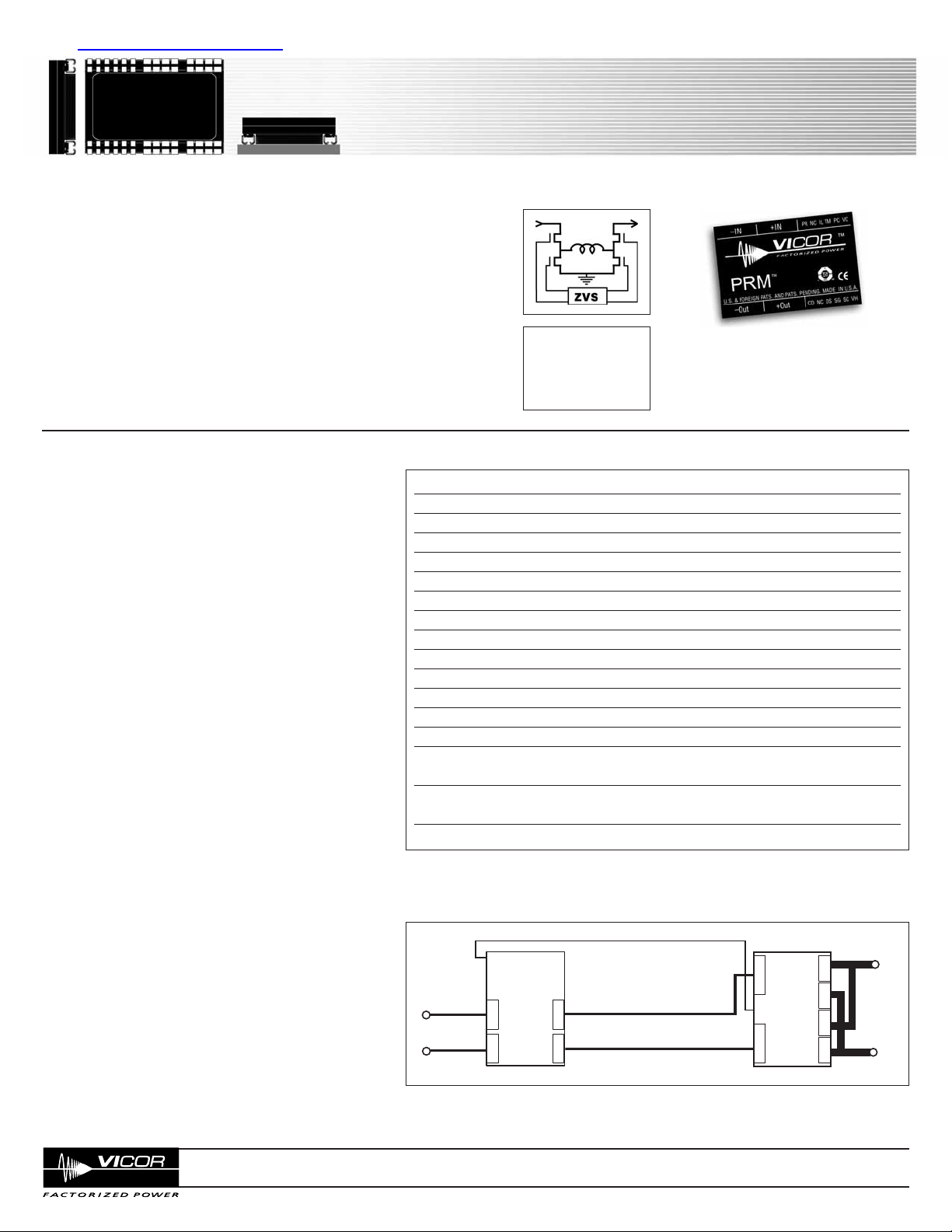
©
V•I ChipTM– PRM-AL
Pre-Regulator Module
Product Description
The V•I Chip Pre-Regulator Module (PRM) is a very
efficient non-isolated regulator capable of both
boosting and bucking a wide range input voltage. It is
specifically designed to provide a controlled Factorized
Bus distribution voltage for powering downstream
V•I Chip Voltage Transformation Modules (VTMs) —
fast, efficient, isolated, low noise Point-of-Load (POL)
converters. In combination, PRMs and VTMs form a
complete DC-DC converter subsystem offering all of
the unique benefits of Vicor’s Factorized Power
Architecture (FPA): high density and efficiency; low
noise operation; architectural flexibility; extremely fast
transient response; and elimination of bulk capacitance
at the Point-of-Load (POL).
In FPA systems, the POL voltage is the product of the
Factorized Bus voltage delivered by the PRM and the
"K-factor" (the fixed voltage transformation ratio) of a
downstream VTM. The PRM controls the Factorized Bus
voltage to provide regulation at the POL. Because VTMs
perform true voltage division and current multiplication,
the Factorized Bus voltage may be set to a value that is
substantially higher than the bus voltages typically
found in "intermediate bus" systems, reducing
distribution losses and enabling use of narrower
distribution bus traces. A PRM-VTM chip set can
provide up to 100 A or 230 W at a FPA system density
of 200 A/in
3
or 460 W/in3— and because the PRM can
be located, or "factorized," remotely from the POL,
these power densities can be effectively doubled.
The PRM described in this data sheet features a unique
"Adaptive Loop" compensation feedback: a single wire
alternative to traditional remote sensing and feedback
loops that enables precise control of an isolated POL
voltage without the need for either a direct connection
to the load or for noise sensitive, bandwidth limiting,
isolation devices in the feedback path.
Actual size
Parameter Values Unit
+In to -In -1.0 to 85.0 Vdc
PC to -In -0.3 to 6.0 Vdc
PR to -In -0.3 to 9.0 Vdc
IL to -In -0.3 to 6.0 Vdc
VC to -In -0.3 to 18.0 Vdc
+Out to -Out -0.3 to 59 Vdc
SC to -Out -0.3 to 3.0 Vdc
VH to -Out -0.3 to 9.5 Vdc
OS to -Out -0.3 to 9.0 Vdc
CD to -Out -0.3 to 9.0 Vdc
SG to -Out 100 mA
Continuous output current 5 Adc
Continuous output power 240 W
Operating junction temperature (M-Grade) -55 to 125 °C
(T-Grade) -40 to 125 °C
Storage temperature (M-Grade) -65 to 150 °C
(T-Grade) -40 to 150 °C
Case temperature during reflow: 208 °C
The P048F048T24AL is used with any 048 input series VTM to provide a regulated and
isolated output.
DC-DC Converter
Absolute Maximum Ratings
PRM
查询V040F033T060供应商
+In
-In
VTM
K
Ro
+Out
-Out
+Out
-Out
+Out
–Out
VH
SC
SG
OS
NC
CD
Factorized
Bus (Vf)
TM
VC
PC
VC
PC
TM
IL
NC
PR
PRM-AL
+In
Vin
–In
Vout
Page 2
vicorpower.com 800-735-6200 V•I Chip Pre-Regulator Module P048F048T24AL Rev. 1.7
Page 2 of 14
PRELIMINARY
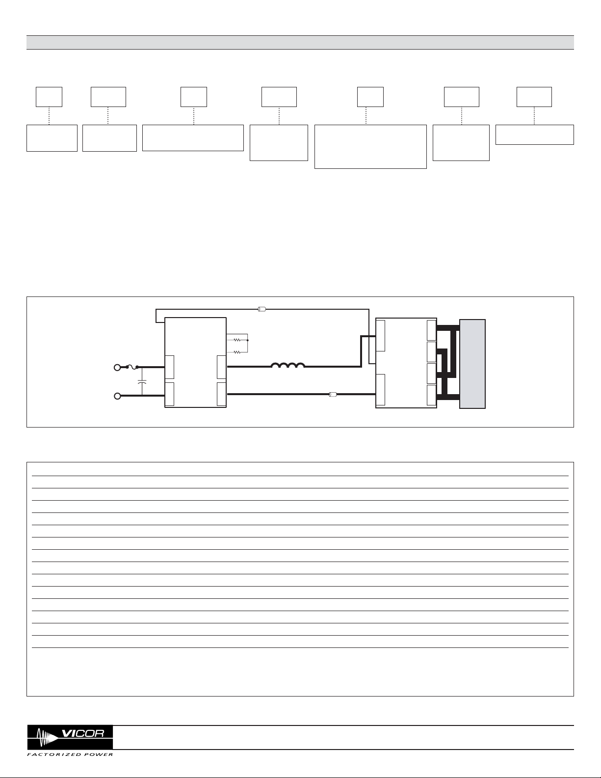
Overview of Adaptive Loop Compensation
Adaptive Loop compensation, illustrated in Figure 1, contributes to
the bandwidth and speed advantage of Factorized Power. The PRM
monitors its output current and automatically adjusts its output
voltage to compensate for the voltage drop in the output
resistance of the VTM. R
OS sets the desired value of the VTM
output voltage, Vout; R
CD is set to a value that compensates for
the output resistance of the VTM (which, ideally, is located at the
point of load). For selection of R
OS and RCD, refer to Table 1 below
or Page 9.
The V•I Chip’s bi-directional VC port :
1. Provides a wake up signal from the PRM to the VTM that
synchronizes the rise of the VTM output voltage to that of the PRM.
2. Provides feedback from the VTM to the PRM to enable the PRM
to compensate for the voltage drop in VTM output resistance, R
O.
Output Power
Designator
(=Pf /10)
P 048 F 048 T 24 AL
Pre-Regulator
Module
Input Voltage
Designator
Product Grade Temperatures (°C)
Grade Storage Operating
T -40 to150 -40 to125
M -65 to150 -55 to125
Configuration
(Fig.21)
Nominal
Factorized Bus
Voltage
AL = Adaptive Loop
Desired Load Voltage (Vdc) VTM P/N
(1)
Max VTM Output Current (A)
(2)
ROS (kΩ)
(3)
RCD (Ω)
(3)
1.0 V048F015T100 100 3.57 26.1
1.2 V048F015T100 100 2.94 32.4
1.5 V048F015T100 100 2.37 39.2
1.8 V048F020T080 80 2.61 35.7
2.0 V048F020T080 80 2.37 39.2
3.3 V040F033T060 60 2.89 32.6
5.0 V048F060T040 40 2.87 33.2
10 V048F120T025 25 2.86 32.9
12 V048F120T025 25 2.37 39.2
15 V048F160T019 18.8 2.49 37.4
24 V048F240T012 12.5 2.37 39.2
28 V048F320T009 9.4 2.74 35.7
36 V048F480T006 6.3 3.16 30.1
48 V048F480T006 6.3 2.37 39.2
Table 1 — Configure your Chip Set using the PRM-AL
Note:
(1) See Table 2 on page 9 for nominal Vout range and K factors.
(2) See “PRM output power vs. VTM output power” on Page 10
(3) 1% precision resistors recommended
Figure 1 — With Adaptive Loop control, the output of the VTM is regulated over the load current range with only a single interconnect between the PRM and
VTM and without the need for isolation in the feedback path.
General Specifications
V•I Chip Pre-Regulator Module
Part Numbering
+Out
–Out
VH
SC
SG
OS
ROS
NC
CD
RCD
Vf =
Vin
VC
PC
TM
IL
NC
PR
PRM-AL
+In
–In
Factorized
Bus (Vf)
(
V
L
Io•Ro
+
K
K
Vo = VL ± 1.0%
+Out
+In
L
O
A
D
VTM
K
Ro
-Out
+Out
-Out
TM
VC
)
PC
-In
Page 3
vicorpower.com 800-735-6200 V•I Chip Pre-Regulator Module P048F048T24AL Rev. 1.7
Page 3 of 14
PRELIMINARY
Parameter Min Typ Max Unit Note
Input voltage range 36 48 75 Vdc
Input dV/dt 1 V/µs
Input undervoltage turn-on 33.8 35.3 Vdc
Input undervoltage turn-off 30.5 31.8 Vdc
Input overvoltage turn-on 75.8 77.3 Vdc
Input overvoltage turn-off 78.8 81.0 Vdc
Input quiescent current 0.5 1 mA PC low
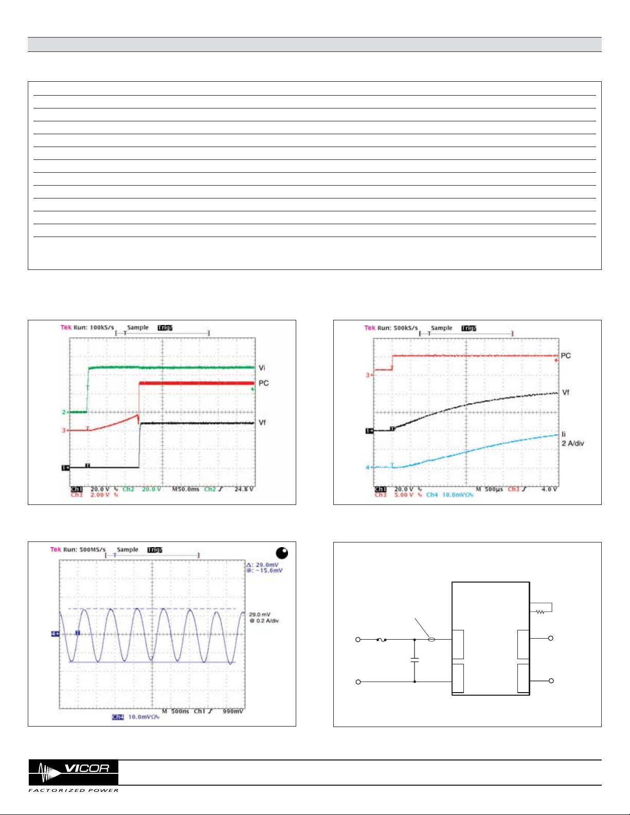
Input current 5.2 Adc
Input reflected ripple current 580 mA p-p See Figures 4 & 5
No load power dissipation 3.0 W
Internal input capacitance 5 µF Ceramic
Recommended external input capacitance 100 µF See Figure 5 for input filter circuit.
Source impedance dependent
Input Specs (Conditions are at 48 Vin, 48 Vf, full load, and 25°C ambient unless otherwise specified)
Figure 3 — Vf turn-on waveform with inrush current – PC enabled at
full load, 48 Vin
Figure 2 — Vf and PC response from power up
Figure 4 — Input reflected ripple current at full load and 48 Vin
Input Waveforms
Figure 5 — Input filter capacitor recommendation
Electrical Specifications
V•I Chip Pre-Regulator Module
+IN
–IN
Reflected
Measurement
10 A
100 μF
Al-Electrolytic
Ripple
VC
PC
TM
IL
NC
PR
PRM-AL
+In
–In
+Out
–Out
VH
SC
SG
OS
NC
CD
2.37 kΩ
+ OUT
– OUT
Page 4
vicorpower.com 800-735-6200 V•I Chip Pre-Regulator Module P048F048T24AL Rev. 1.7
Page 4 of 14
PRELIMINARY
Parameter Min Typ Max Unit Note
Output voltage range 26 48 55 Vdc Factorized Bus voltage (Vf) set by ROS
Output power 0 240 W
Output current 0 5 Adc
DC current limit 5.25 6.0 6.6 Adc IL pin floating
Average short circuit current 0.5 A Auto recovery
Set point accuracy 1.5 %
Line regulation 0.1 0.2 % Low line to high line
Load regulation 0.1 0.2 % No CD resistor
Load regulation (at VTM output) 1.0 2.0 % Adaptive Loop
Current share accuracy 5 10 %
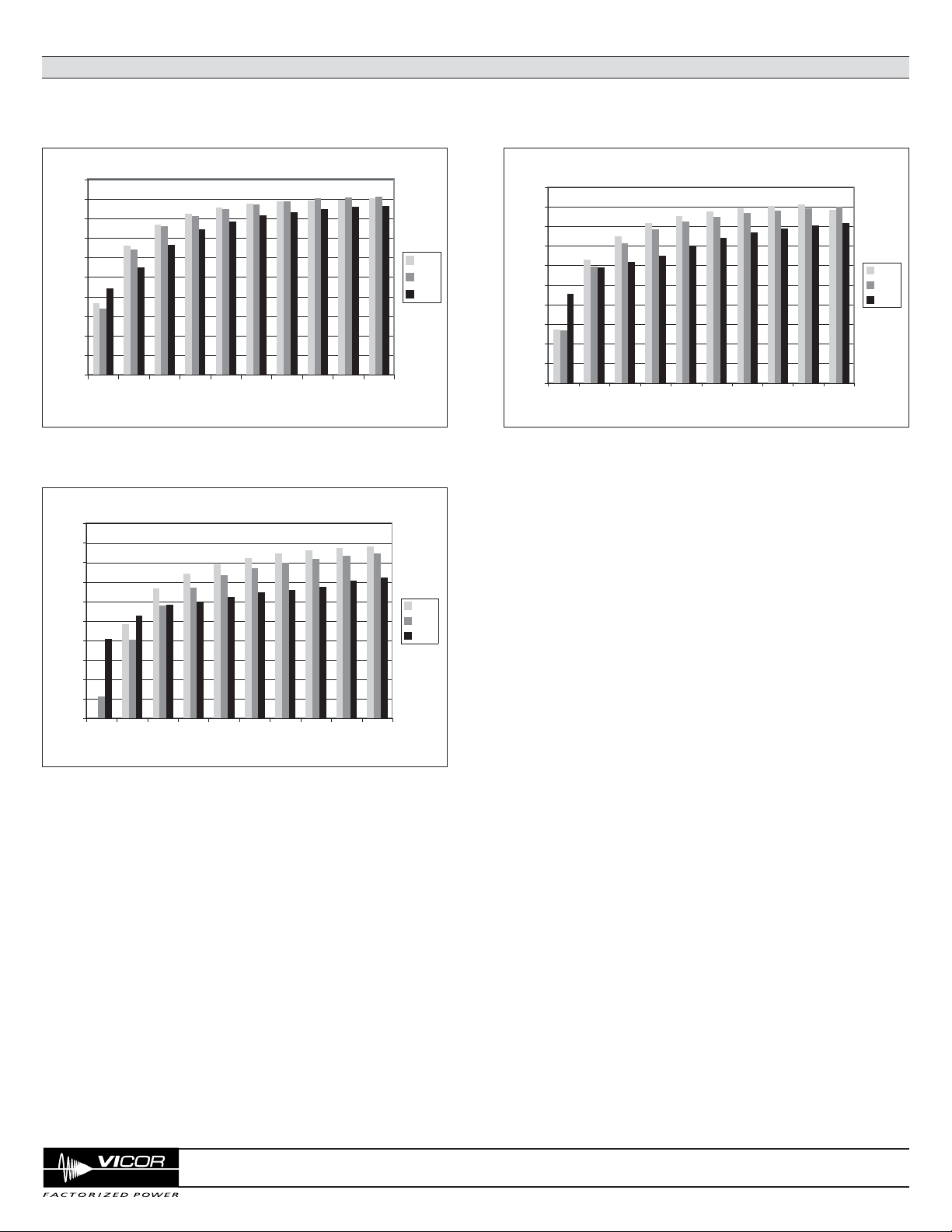
Efficiency
Full load 96 % See Figure 6,7 & 8
Output overvoltage set point 56 59.4 Vdc
Output ripple voltage
No external bypass 2.3 2.5 % Factorized Bus, see figure 13
With 10 µF capacitor 1.0 1.1 % Factorized Bus, see figure 14
Switching frequency 1.35 1.45 1.55 MHz Fixed frequency
Output turn-on delay
From application of power 200 300 ms See Figure 2
From PC pin high 100 µs See Figure 3
Internal output capacitance 5 µF Ceramic
Factorized Bus capacitance 47 µF
Output Specs (Conditions are at 48 Vin, 48 Vf, full load, and 25°C ambient unless otherwise specified)
Electrical Specifications
(continued) V•I Chip Pre-Regulator Module
Page 5
vicorpower.com 800-735-6200 V•I Chip Pre-Regulator Module P048F048T24AL Rev. 1.7
Page 5 of 14
PRELIMINARY
Electrical Specifications
(continued) V•I Chip Pre-Regulator Module
Figure 7 — Efficiency vs. output current at 36 Vf
Figure 8 — Efficiency vs. output current at 26 Vf
Efficiency Graphs
Figure 6 — Efficiency vs. output current at 48 Vf
Efficiency vs. Output Current
98
96
94
92
90
88
86
Efficiency (%)
84
82
80
78
0.5 1.1 1.5 2.0 2.5 3.0 3.5 4.0 4.6 5.0
Output Current (A)
Efficiency vs. Output Current
98
96
94
92
90
88
86
Efficiency (%)
84
82
80
78
0.5 1.0 1.6 2.0 2.5 3.0 3.5 4.0 4.6 5.0
Output Current (A)
Vin
Vin
36V
48V
75V
36V
48V
75V
Efficiency vs. Output Current
98
96
94
92
90
88
86
Efficiency (%)
84
82
80
78
0.5 1.0 1.5 2.0 2.5 3.0 3.5 4.0 4.5 5.0
Output Current (A)
Vin
36V
48V
75V
Page 6

vicorpower.com 800-735-6200 V•I Chip Pre-Regulator Module P048F048T24AL Rev. 1.7
Page 6 of 14
PRELIMINARY
Figure 10 — Transient response; PRM alone, 48 Vin, 0 – 5.0 – 0 A
no load capacitance. Local Loop
Figure 12 — PC during fault – frequency will vary as a function of line
voltage.
Output Waveforms
Figure 11 — Transient response; load change from 40 – 80 – 40 A,
at the output of a K=1/24 VTM with no Vf bus capacitance and 100 µF
load capacitance.
Figure 13 — Output ripple full load no bypass capacitance
Figure 9 — VTM output regulation and Vf bus during load step using
VTM with K = 1/24
Figure 14 — Output ripple full load 10µF bypass capacitance
Page 7

vicorpower.com 800-735-6200 V•I Chip Pre-Regulator Module P048F048T24AL Rev. 1.7
Page 7 of 14
PRELIMINARY
Auxiliary Pins (Conditions are at 48 Vin, 48 Vf, full load, and 25°C ambient unless otherwise specified)
Parameter Min Typ Max Unit Note
VC (VTM Control)
Peak voltage 14 V Referenced to –OUT
PC (Primary Control)
DC voltage 4.8 5.0 5.2 Vdc Referenced to –IN
Module disable voltage 2.3 2.4 Vdc Referenced to –IN
Module enable voltage 2.5 2.6 Vdc
Disable hysteresis 100 mV
Source only after start up; not to be used for
Current limit 1.75 1.90 mA aux. supply; 100 kΩ minimum load
impedance to assure start up.
Enable delay time 100 µs
Disable delay time 1 µs
IL (Current Limit Adjust)
Voltage 1 V
Accuracy ± 15 % Based on DC current limit set point
PR (Parallel Port)
Voltage 0.6 7.5 V Referenced to SG
Source current 1 mA
External capacitance 100 pF
VH (Auxiliary Voltage)
Range 8.7 9.0 9.3 Vdc Maximum source = 5 mA, referenced to SG
Regulation 0.04 %/mA
SC (Secondary Control)
Voltage 1.23 1.24 1.25 Vdc Referenced to SG
Internal capacitance 0.1 µF
External capacitance 0.7 µF
OS (Output Set)
Set point accuracy ± 1.5 % Includes 1% external resistor
Reference offset ± 4 mV
CD (Compensation Device)
External resistance 20 Ω Omit resistor for regulation at output of PRM
Parameter Min Typ Max Unit Note
MTBF
MIL-HDBK-217F 2.2 Mhrs 25°C, GB
Agency approvals (pending)
cTÜVus UL/CSA 60950, EN60950
CE Mark Low voltage directive
Mechanical parameters See mechanical drawing, Figure19
Weight 0.5 / 14 oz / g
Dimensions
Length 1.26 / 32 in / mm
Width 0.87 / 22 in / mm
Height 0.25 / 6,2 in / mm
General Specs
Electrical Specifications
(continued) V•I Chip Pre-Regulator Module
Page 8

vicorpower.com 800-735-6200 V•I Chip Pre-Regulator Module P048F048T24AL Rev. 1.7
Page 8 of 14
PRELIMINARY
Pin / Control Functions
V•I Chip Pre-Regulator Module
+IN / -IN DC Voltage Ports
The V•I Chip maximum input voltage should not be exceeded. PRMs
have internal over / undervoltage lockout functions that prevent
operation outside of the specified input range. PRMs will turn on
when the input voltage rises above its undervoltage lockout. If the
input voltage exceeds the overvoltage lockout, PRMs will shut down
until the overvoltage fault clears. PC will toggle indicating an out of
bounds condition.
+OUT / -OUT Factorized Voltage Output Ports
These ports provide the Factorized Bus voltage output. The –OUT port
is connected internally to the –IN port through a current sense resistor.
The PRM has a maximum power and a maximum current rating and is
protected if either rating is exceeded. Do not short –OUT to –IN.
VC – VTM Control
The VTM Control (VC) port supplies an initial V
CC voltage to
downstream VTMs, enabling the VTMs and synchronizing the rise of
the VTM output voltage to that of the PRM. The VC port also provides
feedback to the PRM to compensate for voltage drop due to the VTM
output resistance. The PRM’s VC port should be connected to the VTM
VC port. A PRM VC port can drive a maximum of two (2) VTM VC ports.
PC – Primary Control
The PRM voltage output is enabled when the PC pin is open circuit
(floating). To disable the PRM output voltage, the PC pin is pulled low.
Open collector optocouplers, transistors, or relays can be used to
control the PC pin. When using multiple PRMs in a high power array,
the PC ports must be tied together to synchronize their turn on.
During an abnormal condition the PC pin will pulse (Fig.12) as the
PRM initiates a restart cycle. This will continue until the abnormal
condition is rectified. The PC should not be used as an auxiliary voltage
supply, nor should it be switched at a rate greater than 1 Hz.
TM – Factory Use Only
IL – Current Limit Adjust
The PRM has a preset, maximum, current limit set point. The IL port
may be used to reduce the current limit set point to a lower value. See
“adjusting current limits” on page 10.
PR – Parallel Port
The PR port signal, which is proportional to the PRM output power,
supports current sharing among PRMs. To enable current sharing, PR
ports should be interconnected. Bypass capacitance should be used
when interconnecting PR ports and steps should be taken to minimize
coupling noise into the interconnecting bus. Please consult Vicor
Applications Engineering regarding additional considerations.
VH – Auxiliary Voltage
VH is a gated, non-isolated, nominally 9 Volt, regulated DC voltage
(see “Auxiliary Pins” specifications, on Page 7) that is referenced to
SG. VH may be used to power external circuitry having a total current
consumption of no more than 5 mA.
SC – Secondary Control
The load voltage may be controlled by connecting a resistor or voltage
source to the SC port referenced to SG. The slew rate of the output
voltage may be controlled by controlling the rate-of-rise of the voltage
at the SC port (e.g., to limit inrush current into a capacitive load).
SG – Signal Ground
This port provides a low inductance Kelvin connection to –IN and
should be used as reference for the OS, CD, SC,VH and IL ports.
OS – Output Set
The application-specific value of the Factorized Bus voltage (Vf) is set
by connecting a resistor between OS and SG. Resistor value selection is
shown in Table 1 on Page 2, and described on Page 9. If no resistor is
connected, the PRM output will be approximately one volt. If set
resistor is not collocated with the PRM, a local bypass capacitor of
~200 pF may be required.
CD – Compensation Device
Adaptive Loop control is configured by connecting an external resistor
between the CD port and SG. Selection of an appropriate resistor
value (see Equation 2 on Page 9 and Table 1 on Page 2) configures the
PRM to compensate for voltage drops in the equivalent output
resistance of the VTM and the PRM-VTM distribution bus. If no resistor
is connected to CD, the PRM will be in Local Loop mode and will
regulate the +OUT / –OUT voltage to a fixed value.
Figure 15 — PRM pin configuration
Signal Name Designation
+IN G1-K1,G2-K2
–IN L1-P1, L2-P2
VC A1,A2
PC B1, B2
TM C1, C2
IL D1, D2
PR F1, F2
VH A3, A4
SC B3, B4
SG C3, C4
OS D3, D4
CD F3, F4
+OUT G3-K3, G4-K4
–OUT L3-P3, L4-P4
AL Version
+OUT
–OUT
4 3 2 1
A
VH
B
SC
C
SG
D
OS
E
NC
F
CD
G
H
J
K
L
M
N
P
VC
A
PC
B
TM
C
IL
D
NC
E
PR
F
G
H
+IN
J
K
L
M
–IN
N
P
Bottom View
Page 9

vicorpower.com 800-735-6200 V•I Chip Pre-Regulator Module P048F048T24AL Rev. 1.7
Page 9 of 14
PRELIMINARY
Output Voltage Setting with Adaptive Loop
The equations for calculating R
OS and RCD to set a VTM output
voltage are:
93100
ROS =
(
VL • 0.8395
)
–
1
(1)
K
RCD =
91238
+ 1
(2)
ROS
VL = Desired load voltage
V
OUT = VTM output voltage
K = VTM transformation ratio
(available from appropriate VTM data sheet)
V
f = PRM output voltage, the Factorized Bus (see Figure 16)
R
O = VTM output resistance
(available from appropriate VTM data sheet)
I
L = Load Current
(actual current delivered to the load)
Output Voltage Trimming (optional)
After setting the output voltage from the procedure above the output
may be margined down (26Vf min) by a resistor from SC-SG using this
formula:
RdΩ =
10000 V
fd
Vfs - Vfd
Where Vfd is the desired factorized bus and Vfs is the set factorized bus.
A low voltage source can be applied to the SC port to margin the load
voltage in proportion to the SC reference voltage.
An external capacitor can be added to the SC port as shown in Figure 16
to control the output voltage slew rate for soft start.
Figure 16 — Adaptive Loop compensation with soft start using the SC port.
Nominal Vout VTM
Range (Vdc) K Factor
0.8
↔
1.6 1/32
1.1
↔
2.2 1/24
1.6
↔
3.3 1/16
2.2
↔
4.4 1/12
3.3
↔
6.6 1/8
4.3
↔
8.8 1/6
6.5
↔
13.4 1/4
8.7
↔
17.9 1/3
13.0
↔
26.9 1/2
17.4
↔
36.0 2/3
26.0
↔
54.0 1
Table 2 — 048 input series VTM K factor selection guide
Application Information
V•I Chip Pre-Regulator Module
+Out
–Out
VH
SC
SG
OS
NC
CD
ROS
RCD
Factorized
Bus (Vf)
V
Vf =
K
L
VC
PC
TM
IL
NC
PR
PRM-AL
+In
Vin
–In
VTM
K
Ro
+Out
-Out
+Out
-Out
L
O
A
D
+In
0.4 μH
(
)
I
L•Ro
+
K
TM
VC
PC
-In
Page 10

vicorpower.com 800-735-6200 V•I Chip Pre-Regulator Module P048F048T24AL Rev. 1.7
Page 10 of 14
PRELIMINARY
Application Information
(continued) V•I Chip Pre-Regulator Module
OVP – Overvoltage Protection
The output Overvoltage Protection set point of the P048K048T24AL is
factory preset for 56 V. If this threshold is exceeded the output shuts
down and a restart sequence is initiated, also indicated by PC pulsing.
If the condition that causes OVP is still present, the unit will again shut
down. This cycle will be repeated until the fault condition is removed.
The OVP set point may be set at the factory to meet unique high
voltage requirements.
PRM output power versus VTM output power
As shown in Figure 17, the P048F048T24AL is rated to deliver 5 A
maximum, when it is delivering an output voltage in the range from
26 V to 48 V, and 240 W, maximum, when delivering an output
voltage in the range from 48 V to 55 V. When configuring a PRM for
use with a specific VTM, refer to the appropriate VTM data sheet. The
VTM input power can be calculated by dividing the VTM output power
by the VTM efficiency (available from the VTM data sheet). The input
power required by the VTM should not exceed the output power
rating of the PRM.
The Factorized Bus voltage should not exceed an absolute limit of
55 V, including steady state, ripple and transient conditions. Exceeding
this limit may cause the internal OVP set point to be exceeded.
Parallel considerations
The PR port is used to connect two or more PRMs in parallel to form a
higher power array. When configuring arrays, PR port interconnection
bypass capacitance must be used at ~1nF per PRM. Additionally one
PRM should be designated as the master while all other PRMs are set
as slaves by shorting their SC pin to SG. The PC pins must be directly
connected (no diodes) to assure a uniform start up sequence. The
factorized bus should be connected in parallel as well.
Adjusting current limit
The current limit can be lowered by placing an external resistor
between the I
L and SG ports (see figure 18 for resistor values). With
the I
L port open-circuit, the current limit is preset to be within the
range specified in the output specifications table on Page 4.
Input fuse recommendations
A fuse should be incorporated at the input to the PRM, in series with
the +IN port. A fast acting fuse, NANO2 FUSE 451/453 Series 10 A
125 V, or equivalent, may be required to meet certain safety agency
Conditions of Acceptability. Always ascertain and observe the safety,
regulatory, or other agency specifications that apply to your specific
application.
Product safety considerations
If the input of the PRM is connected to SELV or ELV circuits, the output
of the PRM can be considered SELV or ELV respectively.
If the input of the PRM is connected to a centralized DC power system
where the working or float voltage is above SELV, but less than or
equal to 75 V, the input and output voltage of the PRM should be
classified as a TNV-2 circuit and spaced 1.3 mm from SELV circuitry or
accessible conductive parts according to the requirements of UL60950,
CSA 22.2 60950, EN60950, and IEC60950.
Applications assistance
Please contact Vicor Applications Engineering for assistance,
1-800-927-9474, or email at apps@vicr.com.
Figure 18 — Calculated external resistor value for adjusting current limit,
actual value may vary.
Figure 17 — P048K048T24AL rating based on Factorized Bus voltage
5.1
5.0
4.9
4.8
4.7
4.6
Current (A)
4.5
4.4
4.3
~
~
0
20
22 24
Safe Operating Area
28 32 36 40 44 48 52
26 30
34
38 42
Factorized Bus Voltage (Vf)
46 50
54
56
58
60
100.00
10.00
Resistance (kΩ)
1.00
12345
Desired PRM Output Current Limit (A)
Page 11

vicorpower.com 800-735-6200 V•I Chip Pre-Regulator Module P048F048T24AL Rev. 1.7
Page 11 of 14
PRELIMINARY
Figure 19—PRM J-Lead mechanical outline
Figure 20— PRM J-Lead PCB land layout information
Mechanical Specifications
(continued) V•I Chip Pre-Regulator Module
22,0
0.87
OUTPUT
32,0
1.26
INPUT
TOP VIEW (COMPONENT SIDE)
6,2
0.25
30,00
(2) X
1.181
26,00
(2) X
1.024
22,00
(2) X
0.866
15,55
0.612
0,45
0.020
NOTES:
1- DIMENSIONS ARE .
2- UNLESS OTHERWISE SPECIFIED, TOLERANCES ARE:
.X/[.XX] = +/-0.25/[.01]; .XX/[.XXX] = +/-0.13/[.005]
3- PRODUCT MARKING ON TOP SURFACE
mm
inch
DXF and PDF files are available on vicorpower.com
(2) X
10,00
0.394
3,01
0.118
OUTPUT
15,99
0.630
C
L
BOTTOM VIEW
3,01
0.118
INPUT
C
L
(4) X
(2) X
8,10
0.319
(2) X
20,00
0.787
(12) X
24,00
0.945
1,10
0.043
(2) X
28,00
1.102
28,00
(4) X
1.102
24,00
(4) X
0.945
20,00
(4) X
0.787
(8) X
1,38
0.054
8,48
0.334
3,26
0.128
TYP
15,74
0.620
VC
PC
TM
IL
NC
PR
-IN +IN
RECOMMENDED LAND PATTERN
(COMPONENT SIDE SHOW)
3,26
0.128
0,51
TYP
0.020
VH
SC
SG
OS
NC
CD
+OUT
-OUT
(4) X
10,00
0.394
22,00
(4) X
0.866
15,96
0.628
NOTES:
1- DIMENSIONS ARE .
2- UNLESS OTHERWISE SPECIFIED, TOLERANCES ARE:
.X/[.XX] = +/-0.25/[.01]; .XX/[.XXX] = +/-0.13/[.005]
(4) X
26,00
1.024
(4) X
mm
inch
30,00
1.181
(24) X
1,48
0.058
DXF and PDF files are available on vicorpower.com
Page 12

vicorpower.com 800-735-6200 V•I Chip Pre-Regulator Module P048F048T24AL Rev. 1.7
Page 12 of 14
PRELIMINARY
Configuration Options
V•I Chip Pre-Regulator Module
Configuration
Standard
(1)
Standard with 0.25"
(Figure 21) Heat Sink
(2)
Effective power density 875 W/in
3
437 W/in
3
Effective Junction-Board
2.4 °C/W 2.4 °C/W
thermal resistanc
Effective Junction-Case
1.1 °C/W N/A
thermal resistance
Effective Junction-Ambient
6.8 °C/W 5.0 °C/W
thermal resistance 300LFM
Note:
(1) Surface mounted to a 2" x 2" FR4 board, 4 layers 2 oz Cu
(2) Heat sink available as a separate item
STANDARD MOUNT
22.0
0.87
32.0
1.26
6.3
0.25
Figure 21—Standard mounting – package F
mm
in
Figure 22—Hole location for push pin heatsink relative to VIC
Symbol Parameter Min Typ Max Unit Note
Over temperature shutdown 125 130 135 °C Junction temperature
Thermal capacity 0.61 Ws/°C
RθJC Junction-to-case thermal impedance 1.1 °C/W
RθJB Junction-to-board thermal impedance 2.1 °C/W
RθJA Junction-to-ambient
(1)
6.5 °C/W
RθJA Junction-to-ambient
(2)
5.0 °C/W
Thermal
Notes:
(1) P048F048T24AL surface mounted to a 2" x 2" FR4 board, 4 layers 2 oz Cu, 300 LFM.
(2) P048F048T24AL with a 0.25"H heatsink surface mounted on FR4 board, 300 LFM.
Page 13

vicorpower.com 800-735-6200 V•I Chip Pre-Regulator Module P048F048T24AL Rev. 1.7
Page 13 of 14
PRELIMINARY
V•I Chip soldering recommendations
V•I Chip modules are intended for reflow soldering processes. The
following information defines the processing conditions required for
successful attachment of a V•I Chip to a PCB. Failure to follow the
recommendations provided can result in aesthetic or functional failure
of the module.
Storage
V•I Chip modules are currently rated at MSL 5. Exposure to ambient
conditions for more than 48 hours requires a 24 hour bake at 125ºC
to remove moisture from the package.
Solder paste stencil design
Solder paste is recommended for a number of reasons, including
overcoming minor solder sphere co-planarity issues as well as simpler
integration into overall SMD process.
63/37 SnPb, either no-clean or water-washable, solder paste should be
used. Pb-free development is underway.
The recommended stencil thickness is 6 mils. The apertures should be
20 mils in diameter for the Inboard (BGA) application and 0.9-0.9:1 for
the Onboard (J-Leaded).
Pick and place
Modules should be placed within ±5 mils.to maintain placement
position, the modules should not be subjected to acceleration greater
than 500 in/sec
2
prior to reflow.
Reflow
There are two temperatures critical to the reflow process; the solder
joint temperature and the module’s case temperature. The solder joint’s
temperature should reach at least 220ºC, with a time above liquidus
(183ºC) of ~30 seconds.
The module’s case temperature must not exceed 208 ºC at anytime
during reflow.
Because of the ΔT needed between the pin and the case, a forced-air
convection oven is preferred for reflow soldering. This reflow method
generally transfers heat from the PCB to the solder joint. The module’s
large mass also reduces its temperature rise. Care should be taken to
prevent smaller devices from excessive temperatures. Reflow of
modules onto a PCB using Air-Vac-type equipment is not recommended
due to the high temperature the module will experience.
Inspection
The solder joints should conform to IPC 12.2
• Properly wetted fillet must be evident.
• Heel fillet height must exceed lead thickness plus solder thickness.
Removal and rework
V•I Chip modules can be removed from PCBs using special tools such
as those made by Air-Vac. These tools heat a very localized region of
the board with a hot gas while applying a tensile force to the
component (using vacuum). Prior to component heating and removal,
the entire board should be heated to 80-100ºC to decrease the
component heating time as well as local PCB warping. If there are
adjacent moisture-sensitive components, a 125ºC bake should be used
prior to component removal to prevent popcorning. V•I Chip modules
should not be expected to survive a removal operation.
Figure 22—Thermal profile diagram
Figure 23— Properly reflowed V•I Chip J-Lead
Application Information
V•I Chip Pre-Regulator Module
239
Joint Temperature, 220ºC
183
165
degC
91
16
Soldering Time
Case Temperature, 208ºC
Page 14

vicorpower.com 800-735-6200 V•I Chip Pre-Regulator Module P048F048T24AL Rev. 1.7
11/05
Vicor’s comprehensive line of power solutions includes high density AC-DC
and DC-DC modules and accessory components, fully configurable AC-DC
and DC-DC power supplies, and complete custom power systems.
Information furnished by Vicor is believed to be accurate and reliable. However, no responsibility is assumed by Vicor
for its use. Vicor components are not designed to be used in applications, such as life support systems, wherein a
failure or malfunction could result in injury or death. All sales are subject to Vicor’s Terms and Conditions of Sale,
which are available upon request.
Specifications are subject to change without notice.
Intellectual Property Notice
Vicor and its subsidiaries own Intellectual Property (including issued U.S. and Foreign Patents and pending
patent applications) relating to the products described in this data sheet. Interested parties should contact
Vicor's Intellectual Property Department.
Vicor Corporation
25 Frontage Road
Andover, MA, USA 01810
Tel: 800-735-6200
Fax: 978-475-6715
email
Vicor Express: vicorexp@vicr.com
Technical Support: apps@vicr.com
Warranty
Vicor products are guaranteed for two years from date of shipment against defects in material or workmanship when in
normal use and service. This warranty does not extend to products subjected to misuse, accident, or improper application
or maintenance. Vicor shall not be liable for collateral or consequential damage. This warranty is extended to the original
purchaser only.
EXCEPT FOR THE FOREGOING EXPRESS WARRANTY, VICOR MAKES NO WARRANTY, EXPRESS OR IMPLIED, INCLUDING, BUT
NOT LIMITED TO, THE WARRANTY OF MERCHANTABILITY OR FITNESS FOR A PARTICULAR PURPOSE.
Vicor will repair or replace defective products in accordance with its own best judgement. For service under this warranty,
the buyer must contact Vicor to obtain a Return Material Authorization (RMA) number and shipping instructions.
Products returned without prior authorization will be returned to the buyer. The buyer will pay all charges incurred in
returning the product to the factory. Vicor will pay all reshipment charges if the product was defective within the terms
of this warranty.
Information published by Vicor has been carefully checked and is believed to be accurate; however, no responsibility is
assumed for inaccuracies. Vicor reserves the right to make changes to any products without further notice to improve
reliability, function, or design. Vicor does not assume any liability arising out of the application or use of any product or
circuit; neither does it convey any license under its patent rights nor the rights of others. Vicor general policy does not
recommend the use of its components in life support applications wherein a failure or malfunction may directly threaten
life or injury. Per Vicor Terms and Conditions of Sale, the user of Vicor components in life support applications assumes
all risks of such use and indemnifies Vicor against all damages.
 Loading...