

Page 1
Design Guide & Applications Manual
For Maxi, Mini, Micro Family DC-DC Converter
and Accessory Modules
Page 2

Table of Contents
Maxi, Mini, Micro Family DC-DC Converters Section Pages
High Density DC-DC Converter Technology 1 2 – 4
Control Pin Functions and Applications 2 5 – 11
Design Requirements 3 12 – 17
EMC Considerations 4 18 – 19
Current Sharing in Power Arrays 5 20 – 24
Thermal Performance Information 6 25 – 30
Accessory Modules
Autoranging Rectifier Module (ARM) 7 31 – 35
Filter / Autoranging Rectifier Module (FARM) 8 36 – 40
Modular AC Front-end System (ENMod) 9 41 – 47
High Boost HAM 10 48 – 52
Filter Input Attenuator Module (FIAM) Family 11 53 – 55
Output Ripple Attenuator Module (MicroRAM) 12 56 – 61
Recommended Soldering Methods
Lead Free Pins (RoHS) 13 62 – 66
TIn Lead Pins 14 67 – 71
Mounting Options
Surface Mount Socketing System (SurfMate) 15 72 – 75
Through-hole Socket-mount System (InMate) 16 76 – 79
Glossary of Technical Terms 17 80 – 87
Maxi, Mini, Micro Design Guide Rev 4.9 vicorpower.com
Page 1 of 88
Apps. Eng. 800 927.9474 800 735.6200
Page 3
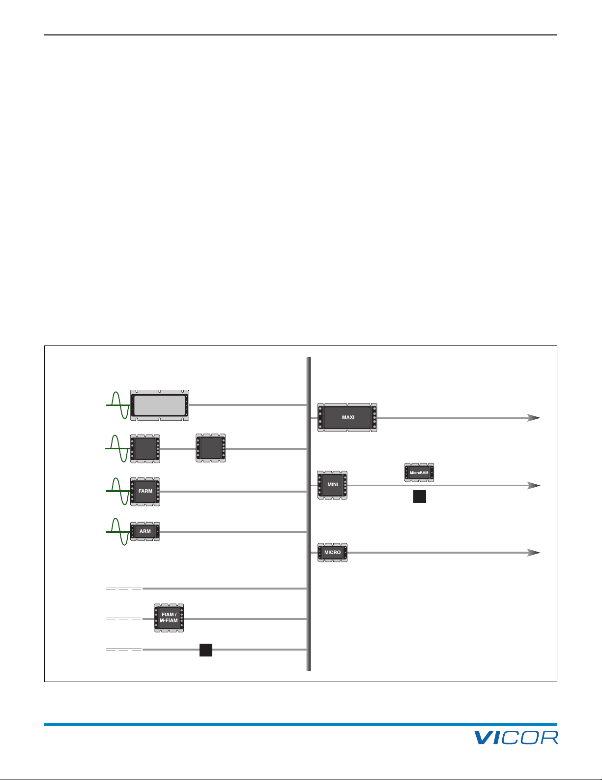
1. High Density DC-DC Converter Technology
AC-DC Products
DC-DC Products
Universal
85 – 264 Vac
Autoranging
90 – 132 Vac
180 – 264 Vac
Autoranging
90 – 132 Vac
180 – 264 Vac
Autoranging
115 – 230 Vac
Input
Nominal Input
18 – 425 Vdc
28 Vdc, 48 Vdc,
270 Vdc
24 Vdc, 28 Vdc,
48 Vdc
Harmonic Attenuator Module
Unity Power Factor
Up to 675 W
per module
Filter / Autoranging Rectifier Module
Up to 1,000 W
Autoranging Rectifier Module
Up to 1,500 W
Front-end System
for EN Compliance
Up to 550 W
Transient Protection,
Inrush Current Limiting EMI Filter
Up to 25 A
Active EMI Filter
Up to 576 W @ 48 V
DC-DC Converter
Up to 600 W per module
1 – 54 Vdc
M
INIHAM
FARM3
QPI
DC-DC Converter
Up to 300 W per module
1 – 48 Vdc
DC-DC Converter
Up to 150 W per module
1 – 48 Vdc
Single wire paralleling for
high power, fault tolerant arrays.
Output Ripple Attenuation Module
combines active and passive filtering.
QPO provides active filtering to
achieve differential noise attenuation.
QPO
DC-DC Products
High Boost
HAM
or Maxi, Mini, Micro Family DC-DC Converters and Configurable Power Supplies
Design Guide & Applications Manual
F
The Maxi, Mini, Micro Family of DC-DC converters are an
integral part of the company’s overall component power
solution strategy, (Figure 1–1), which includes advanced
actory and design automation. The modules are available
f
in an unlimited variety of standard versions, to the extent
hat the line between custom and standard DC-DC
t
converter bricks becomes almost indistinguishable.
The design of the control, magnetic, switching, and
packaging elements of the module resulted in a
component with a power density of up to 120 W/in
3
(7,3 W/cm3) in three package sizes:
Maxi 4.6" x 2.2" x 0.5" (117 x 55,9 x 12,7 mm)
Mini 2.28" x 2.2" x 0.5"(57,9 x 55,9 x 12,7 mm)
Micro 2.28" x 1.45" x 0.5"(57,9 x 36,8 x 12,7 mm)
The modules have one-third the number of parts of their
predecessors.
While the natural by-products of this reduction in parts
count has improved reliability and lower cost, the extra
space also means that the bulk of the converter can now
be devoted almost exclusively to the power train (i.e., the
magnetic and switching elements at the core of the design).
Resistors can be used to trim the output voltage up or
down, if necessary. Six pin styles, three baseplate options,
and a variety of data collection and reporting options are
available. The devices have an operating temperature
range of –55°C to 100°C and come in five product
grades – E, C, T, H, and M.
Other specifications include a typical no-load to full-load
regulation of ±0.5%, a programmable output of 10% to
110%, conversion efficiencies of up to 92% depending
on the voltage combination and power level chosen, and
an input-to-output isolation test voltage of 3,000 Vrms
(4,242 Vdc). All models are parallelable with N+M fault
tolerance and current sharing. Paralleling architectures
feature DC or AC-coupled interface.
Figure 1–1 — Component power solutions with the Maxi, Mini, Micro Family
Maxi, Mini, Micro Design Guide Rev 4.9 vicorpower.com
Page 2 of 88
Apps. Eng. 800 927.9474 800 735.6200
Page 4
Design Guide & Applications Manual
or Maxi, Mini, Micro Family DC-DC Converters and Configurable Power Supplies
F
1. High Density DC-DC Converter Technology
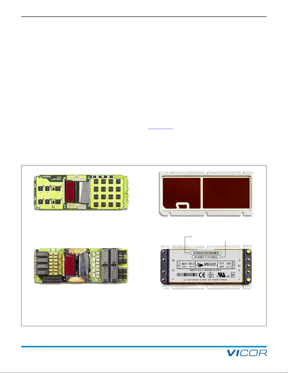
Key to the design of Maxi, Mini, Micro converters is its
high level of component-level integration. (Figure 1–2)
With the aid of hybrid technology, the device packs all
ontrol functions and active circuitry into two (primary
c
and secondary side) ICs occupying a total volume of less
han 1/10 in
t
3
(
1,6 cm
3
each.
)
With Maxi, Mini, Micro devices, the plated-cavity transformer cores use copper armor, plated onto the ferrite
core, to more closely confine the magnetic flux to couple
widely separated primary and secondary windings. The
wider separation provides greater isolation and therefore
lowers input-to-output parasitic capacitance and noise.
The plated cavity also serves to conduct heat away from
the transformer to the baseplate, thus increasing the
power-handling capability of the power train and minimizing temperature rise.
The power-train assembly is contained between the
baseplate and a terminal-block assembly, with input and
output pins recessed. This allows the converter body to be
mounted into an aperture in the PCB to reduce the height
above board. The modules may be wave soldered or
lugged into through-hole or surface-mount sockets.
p
The Maxi, Mini, Micro devices use a proprietary, low-noise,
integrated power device that has an order of magnitude
lower parasitic effect.
The advances made in the overall design of the Maxi,
Mini, Micro Family DC-DC converters have been complemented by equally significant advances in the technology
used to manufacture them. Vicor invested in a custom,
fully-automated assembly line specifically designed for the
assembly of Maxi, Mini, Micro power components. To
further augment its Maxi, Mini, Micro product offering,
Vicor has created an online user-interface tool,
PowerBenchTM, that allows customers to specify DC-DC
module requirements anytime, anywhere via the internet.
Bottom View
• Standard MLP power devices
• Efficient pick-and-place assembly
Top View
• Surface mount components for greater
manufacturing efficiency
• Standard reflow process
Figure 1–2 — Maxi assembly shows high level of integration.
Maxi, Mini, Micro Design Guide Rev 4.9 vicorpower.com
Page 3 of 88
Apps. Eng. 800 927.9474 800 735.6200
Baseplate
• Simplified baseplate construction
Serial No. & Date Code
Complete Assembly
• Insert molded terminal block for more
accurate pin positioning
• One piece cover with label
• Encapsulated for superior thermal performance
Model Number
Page 5
1. High Density DC-DC Converter Technology
+ OUT
+ SENSE*
SC
– OUT
– SENSE*
+ IN
PC
PR
– IN
Primary Control IC
Secondary Control IC
or Maxi, Mini, Micro Family DC-DC Converters and Configurable Power Supplies
F
Design Guide & Applications Manual
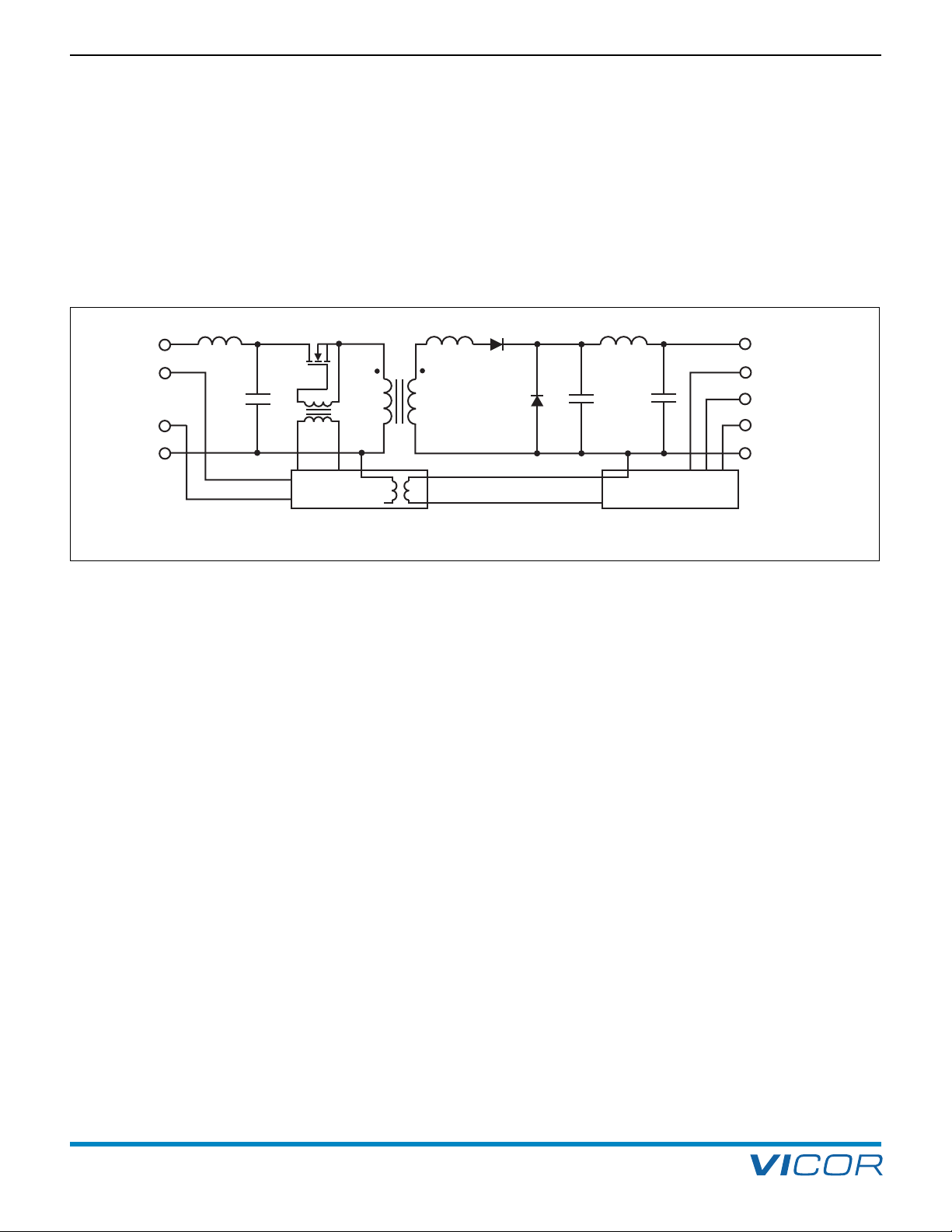
The Maxi, Mini, Micro’s ZCS / ZVS power-processing
architecture (Figure 1–3) enables efficient, low-noise,
high-frequency operation. The main switch is common
rain for improved thermal and noise management,
d
the reset switch located within the primary control IC
s common source for ease of control.
i
The control circuitry is integrated into two (primary and
secondary side) ICs. The result is a significant reduction in
parts with the ensuing savings in cost and increase in
reliability. This integration also provides extra room for
the power train.
Maxi, Mini, Micro transformers place the primary and
secondary windings far apart, but contain the magnetic
flux using a copper armor plated onto the ferrite core.
The armor also conducts excess heat to the baseplate.
Figure 1–3 — Maxi, Mini, Micro: Basic power train and control (*Not included in Micro family)
Maxi, Mini, Micro Design Guide Rev 4.9 vicorpower.com
Page 4 of 88
Apps. Eng. 800 927.9474 800 735.6200
Page 6
Design Guide & Applications Manual
+IN
PC
PR
–IN
4 kΩ
"Module
Enabled"
+IN
PC
PR
–IN
Disable
Disable = PC <2.3 V
+OUT
+S
SC
–S
– O U T
+IN
PC
PR
–IN
Input Undervoltage
2-20 ms typ.
f
(V
IN
)
Auto
Restart
5.7 Vdc
(0-3 mA)
50 Ω
SW2
SW3
1.23
Vdc
6 K
1 K
SW1
S
W1, 2, & 3
shown in
"Fault" position
Input Overvoltage (See Note 1)
Overtemperature
Module Faults
1
Not applicable for 300 Vdc input family
1 M
Input Undervoltage
Input Overvoltage
[a]
Over Temperature
Module Faults
2-20 ms typ.
f(VIN)
Auto
Restart
5.7 Vdc
(0-3 mA)
50 Ω
SW2
SW3
1.23
Vdc
6 K
1 K
SW1
SW1, 2, & 3 shown
in "Fault" position
+OUT
SC
–OUT
+IN
PC
PR
–IN
[a]
Not applicable for 300 Vdc Input family
1 M
or Maxi, Mini, Micro Family DC-DC Converters and Configurable Power Supplies
F
PRIMARY CONTROL (PC PIN)
2. Control Pin Functions and Applications
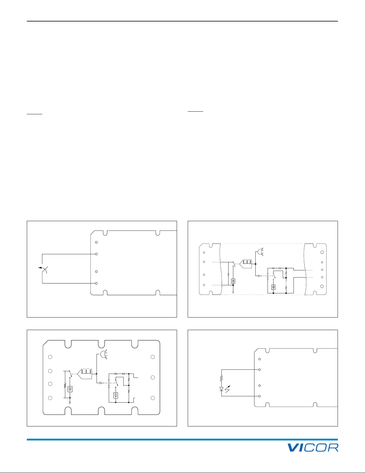
Module Enable / Disable. The module can be disabled
y pulling the PC below 2.3 V with respect to the –Input.
b
This should be done with an open-collector transistor,
relay, or optocoupler. Multiple converters may be disabled
with a single transistor or relay via “ORing” diodes. When
using a mechanical switch or relay to control the PC pin,
please ensure that the contacts are properly debounced
with a capacitor (10 nF max.) to avoid switch bounce.
: Do not exceed a repetitive on / off rate of
NOTE
1 Hz to the PC pin or input voltage pins.
An optocoupler must be used when converters are located
on different PC boards, when a common-mode inductor
is used directly at the module input, or when the distance
between the converters would cause excessive voltage
drops. Under no circumstances should the PC pin be
pulled negative more than a diode drop below the module
–IN. (Figure 2–1) When the PC pin is pulled low the PC
current will pulse similar to the PC voltage shown in
Figure 2–4. When the outputs of two or more converters
are connected in a parallel array to increase system power
the converters should be “group enabled” to ensure that
all the converters start at the same time. The PC pins of all
converters in the array should be controlled by an external
circuit which will enable the converters once the input
oltage is within the normal operating range.
v
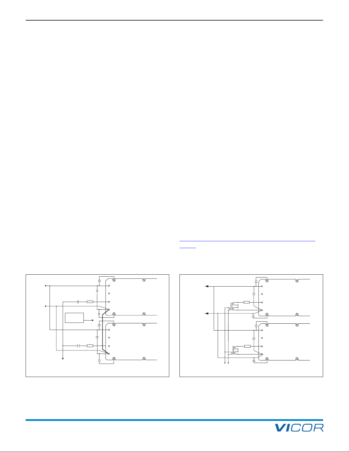
Primary Auxiliary Supply. At 5.75 V, the PC can source
p to 1.5 mA. In the example shown in Figure 2–3, PC
u
powers a LED to indicate the module is enabled.
Another example of an isolated on-state indicator is
shown in Figure 2–5.
NOTE
: When the module has detected a fault or
when the input voltage is above or below the
normal operating range the PC voltage will pulse.
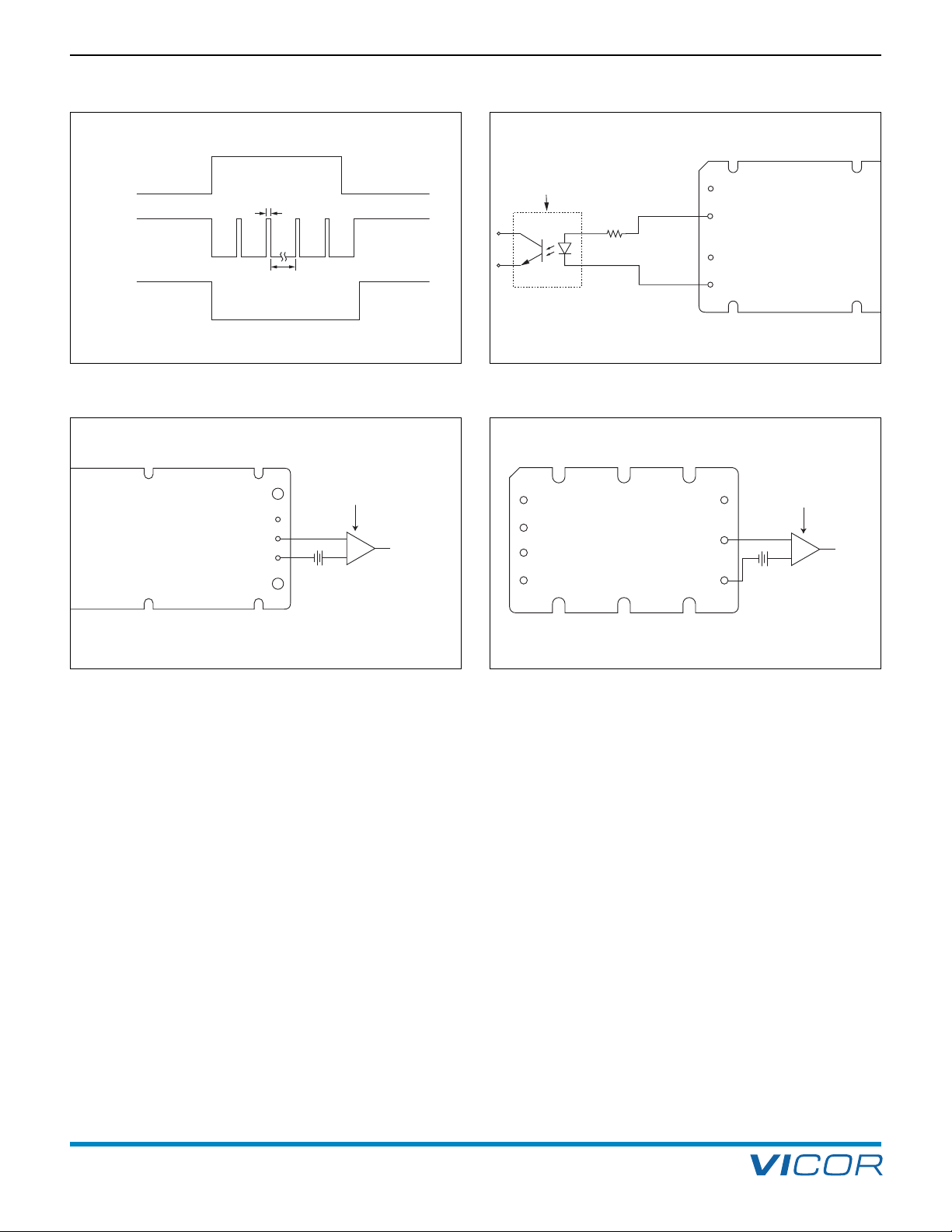
Module Alarm. The module contains “watchdog” circuitry
that monitors input voltage, operating temperature, and
internal operating parameters. (Figures 2–2a and 2–2b) If
any of these parameters is outside their allowable
operating range, the module will shut down and PC will
go low. (Figure 2–4) Then PC will periodically go high and
the module will check to see if the fault (as an example,
input undervoltage) has cleared. If the fault has not been
cleared, PC will go low again and the cycle will restart.
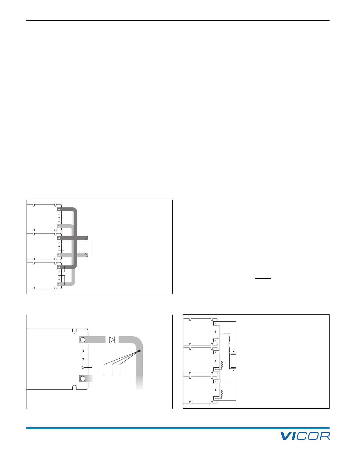
The SC pin will go low when a fault occurs and return to
its normal state after the fault has been cleared. An example
of using a comparator for monitoring on the secondary is
shown in Figures 2–6a and 2–6b.
Figure 2–1 — Module Enable / Disable
Figure 2–2b — PC and SC module alarm logic (Micro)
Maxi, Mini, Micro Design Guide Rev 4.9 vicorpower.com
Page 5 of 88
Figure 2–2a — PC and SC module alarm logic (Maxi / Mini)
Apps. Eng. 800 927.9474 800 735.6200
Figure 2–3 — LED on-state indicator
Page 7
2. Control Pin Functions and Applications
+IN
PC
PR
–IN
Optocoupler
4 kΩ
Alarm
1.00V
+OUT
+
S
SC
–S
–OUT
C
omparator
Alarm
1.0 0 V
+OUT
SC
–OUT
+IN
PC
PR
–IN
Comparator
2–20 ms typ.
Fault
SC
PC
1.23 V
5.7 V
4
0 μs typ.
or Maxi, Mini, Micro Family DC-DC Converters and Configurable Power Supplies
F
Design Guide & Applications Manual
Figure 2–4 — PC / SC module alarm timing Figure 2–5 — Isolated on-state indicator
Figure 2–6a — Secondary side on-state (Maxi / Mini) Figure 2–6b — Secondary side on-state (Micro)
PARALLEL BUS (PR PIN)
A unique feature has been designed into Vicor Maxi, Mini,
Micro converter modules that facilitates parallel operation
for power expansion or redundancy. The PR pin is a bidirectional port that transmits and receives information
between modules. The pulse signal on the parallel (PR)
bus serves to synchronize the high-frequency switching of
each converter which in turn forces them to load share.
These modules possess the ability to arbitrate the leadership role; i.e., a democratic array. The module that
assumes command transmits the sync pulse on the parallel
bus while all other modules on the bus listen. In the event
of a failure of the lead module, the array “elects” a new
leader with no interruption of the output power.
Connection methods for the PR bus include:
1. AC-coupled single-wire interface: All PR pins are
connected to a single communication bus through
0.001 µF (500 V) capacitors. This interface supports
current sharing and is fault tolerant except for the
communication bus. (Figure 2–7) This method may
normally be used with a maximum of three converters.
2. Transformer-coupled interface: Modules or arrays of
modules may also be interfaced to share a load while
providing galvanic isolation between PR pins via a
transformer-coupled interface. For large arrays,
buffering may be required. The power source for the
buffer circuit may be derived from the PC pins. For
arrays of four or more modules, the transformer
coupled interface is recommended. (Figure 2–8)
Maxi, Mini, Micro Design Guide Rev 4.9 vicorpower.com
Page 6 of 88
Apps. Eng. 800 927.9474 800 735.6200
Page 8
Design Guide & Applications Manual
+IN
PC
PR
–IN
+IN
PC
PR
–IN
Module 2
Module 1
+
Parallel
Bus
–
0.2 µF
0.001 µF
0.2 µF
0.001 µF
Low inductance
ground plane
or bus
4.7 nF
4.7 nF
4.7 nF
4.7 nF
Z1*
Z1*
+IN
PC
PR
–IN
+IN
PC
PR
–IN
Module 2
Module 1
T1
T2
+
–
0.2 µF
0.2 µF
Parallel
Bus
4.7 nF
4.7 nF
4.7 nF
4.7 nF
Z1*
Z1*
or Maxi, Mini, Micro Family DC-DC Converters and Configurable Power Supplies
F
PARALLEL OPERATION CONSIDERATIONS
2. Control Pin Functions and Applications
are must be taken to avoid introducing interfering signals
C
(noise) onto the parallel bus that may prevent proper load
sharing between modules, instability, or module failure.
One possible source of interference is input ripple current
onducted via the + and –Input power pins. The PR signal
c
and DC power input share a common return, which is the
–Input pin. Steps should be taken to decouple AC components of input current from the parallel bus. The input to
each converter (designated as + and – pins on the input
side of the module) should be bypassed locally with a
0.2 µF ceramic or film capacitor. This provides a shunt
path for high frequency input ripple current. A Y-rated
4,700 pF capacitor should be connected between both
the + and –Input pins and baseplate of each module, thus
creating a shunt path for common-mode components of
current. Attention to the PC board artwork should minimize
the parasitic impedance between –Input pins of parallel
modules to ensure that all PR pins are referenced to the
same potential, or use a transformer coupled interface.
Modules should be placed physically close to each other
and wide copper traces (0.75 in./19 mm, 2 oz. copper)
should be used to connect power input pins. A dedicated
layer of copper is the ideal solution.
Some applications require physical separation of paralleled
modules on different boards, and/or input power from
separate sources. For applications using separate sources,
please refer to the “Hot-Swap Capability Eliminates
Downtime” application note on Vicor’s website. In these
cases, transformer coupling of the PR signal, per Figure 2–8,
is required to prevent inter-module common-mode noise
rom interfering with the sync pulse transmission. High-
f
speed buffering may be required with large arrays or if the
distance between modules is greater than a few inches.
This is due to the fact that all modules, except the one
hat’s talking, are in the listening mode. Each listener
t
presents a load to the master (talker), which is approximately 500 Ω shunted by 30 pF capacitance. Long leads
for the interconnection introduce losses and parasitic
reactance on the bus, which can attenuate and distort the
sync pulse signal. The bandwidth of the bus must be at
least 60 MHz and the signal attenuation less than 2 dB.
In most cases, transformer coupling without buffering is
adequate. Many applications may benefit from the addition
of Z1, in series with the PR Pin of each converter. A low Q 33 Ω
@ 100 Mhz ferrite bead or a 5 - 15 Ohm resistor may be
used to improve the PR signal waveform. Although this is
not a requirement, it can be very helpful during the debug
stage of large converter arrays to help improve the PR
pulse wave shape and reduce reflections. Again, careful
attention must be given to layout considerations. When
the outputs of two or more converters are connected in a
parallel array to increase system power the converters
should be “group enabled” to ensure that all the converters start at the same time. The PC pins of all converters in
the array should be controlled by an external circuit which
will enable the converters once the input voltage is within
the normal operating range. Please consult with
Applications Engineering at any Vicor Technical Support
Center for additional information.
Figure 2–8 — Transformer-coupled interface
Apps. Eng. 800 927.9474 800 735.6200
Figure 2–7 — AC coupled single-wire interface
Maxi, Mini, Micro Design Guide Rev 4.9 vicorpower.com
Page 7 of 88
Page 9
2. Control Pin Functions and Applications
Module 2
Module 1
Module N+1
+OUT
+S
SC
–S
–OUT
Load
+S
–
S
+S
–S
+S
–S
+OUT
+S
SC
–S
–OUT
+OUT
+S
SC
–S
–OUT
+OUT
+S
SC
–S
–OUT
+Sense from
other modules
in the array
+OUT
SC
–OUT
L
O
A
D
Plane
Ground
Plane
Module #1
Designated
Master
Module #2
trimmed
down 2 %
Module #3
trimmed
down 4 %
+OUT
SC
–OUT
+OUT
SC
–OUT
CONTROL FUNCTIONS AND OUTPUT CONSIDERATIONS
or Maxi, Mini, Micro Family DC-DC Converters and Configurable Power Supplies
Design Guide & Applications Manual
F
arallel Operation (PR Pin). The PR pin supports paral-
P
leling for increased power with N+1or N+M redundancy.
Modules of the same part number will current share if all
PR pins are suitably interfaced. Figures 2–9 and 2–10
how connections for the Maxi and Mini modules; Figure
s
2–11 shows connections for Micro array. Applications
containing two or more Micro modules must define a
designated master (talker) by stagger trimming the output
voltage of each subsequent module down by at least 2%,
or setting the remaining Micro modules in the system as
designated listeners by connecting the SC pin to the
negative output pin.
PR Pin Considerations. When paralleling modules, it is
important that the PR signal is communicated to all
modules within the parallel array. Modules that do not
receive a PR pulse in a parallel array will not current share
and may be damaged by running in an over-power
condition.
The +Out and –Out power buses
•
hould be designed to minimize and
s
balance parasitic impedance from
each module output to the load.
• The +Sense pins should be tied to the same
point on the +Out power bus; (Figure 2-10)
the –Sense pins should be tied to the same
point on the –Out power bus.
• At the discretion of the power system
designer, a subset of all modules within
an array may be configured as slaves
by shorting SC to –S.
• ORing diodes may be inserted in series
with the +OUT pins of each module to
provide module output fault tolerance.
Figure 2–9 — N+1 module array output connections (Maxi and Mini)
ll modules in an array must be of the same part
A
number.Series connection of outputs is accomplished
without connecting the PR pins and allowing each module
to regulate its own output voltage. Since the same current
asses through the output of each module with the series
p
connection, power sharing is inherent. Series connection
of inputs requires special precautions, please contact
Applications Engineering for assistance.
Array Output Overvoltage Protection (OVP). In order
to maintain the highest possible uptime of a parallel array
the converters use an output overvoltage protection
system (OVP) that is highly resistant to false tripping. For
the converter to shut down due to an OVP condition two
conditions must be satisfied (logical AND);
1. The voltage at the output terminals must be greater
than the OVP set point.
2. The secondary control IC within the converter must be
requesting a power conversion cycle from the internal
primary control IC.
By using this logic, false tripping of individual converters
due to externally induced OVP conditions such as load
dumps or, being driven by an external voltage source at
the output terminals is minimized.
Modules connected in a parallel array rely on the active
master module for OVP of the entire array. Modules acting
as boosters (slaves) in the array are receiving external
requests for power conversion cycles (PR pulse) and will
not shut down from an OVP condition. Therefore it is
imperative that the + and -Output pins of modules
connected in a parallel array never
be allowed to become
open circuited from the output bus. An open circuit at the
output terminals will result in terminal voltages far in
excess of the normal rating causing permanent damage
to the module and possible hazardous conditions.
Figure 2–10 — ORing diodes connections (Maxi and Mini)
Maxi, Mini, Micro Design Guide Rev 4.9 vicorpower.com
Page 8 of 88
Figure 2–11 — Parallel module array output connections (Micro)
Apps. Eng. 800 927.9474 800 735.6200
• The +Out and –Out power buses should
be designed to minimize and balance
parasitic impedance from each module
output to the load.
• At the discretion of the power system
designer, a subset of all modules within
an array may be configured as slaves
by shorting SC to –Out.
• Do not use output ORing diodes
with parallel arrays of the Micro.
Page 10

Design Guide & Applications Manual
or Maxi, Mini, Micro Family DC-DC Converters and Configurable Power Supplies
F
CONTROL FUNCTIONS, SECONDARY CONTROL (SC PIN)
utput Voltage Programming. The output voltage of
O
the converter can be adjusted or programmed via fixed
resistors, potentiometers or DACs.
Trim Down. The converter is not
a constant power
device; it has a constant current limit. Hence, available
output power is reduced by the same percentage that
output voltage is trimmed down. Do not exceed maximum
rated output current. The trim down resistor must be
connected to the –S pin (–Out pin on a Micro). (Figures
2–12a and 2–12b)
Trim Up. The converter is rated for a maximum delivered
power. To ensure that maximum rated power is not
exceeded, reduce maximum output current requirement
in the application by the same percentage increase in
output voltage. The trim up resistor must be connected to
the +S pin (+OUT pin on a Micro.) Do not trim the
converter above maximum trim range (+10%) or the
output over voltage protection circuitry may be activated.
(Figures 2–13a and 2–13b)
SC Pin and Output Voltage Trimming. If no connection
is made to the SC pin, the SC pin voltage will be 1.23 V
referenced to –S (-OUT pin on a Micro) and the output of
the converter will equal the nominal output voltage. When
the SC pin voltage is set by an external source such as a
D/A converter, the % change in SC will be equal the %
change in the output voltage.
For example, an application requires a +10, 0% (nominal),
and a –15% output voltage adjustment for a 48 V output
converter. Referring to the table below, the voltage that
should be applied to the SC pin would be as follows:
2. Control Pin Functions and Applications
or systems that require an adjustable output voltage, it is
F
good practice to limit the adjustment range to a value
only slightly greater than that required. This will increase
the adjustment resolution while reducing noise pickup.
It is recommended that the maximum rate of change
applied to the SC pin be limited to 30 Hz, sinusoidal.
Small step-up changes are permissible; however, the
resultant change in the output voltage can create significant current demands due to charge requirements of both
the internal and external output capacitance. In no case
should the converter be driven beyond rated continuous
output current. The response to programming a lower
output voltage is limited by the energy stored in both the
internal and external output capacitance and the load.
The converter cannot sink current to lower the output
voltage other than a minimal internal preload.
Contact
to be dynamically trimmed.
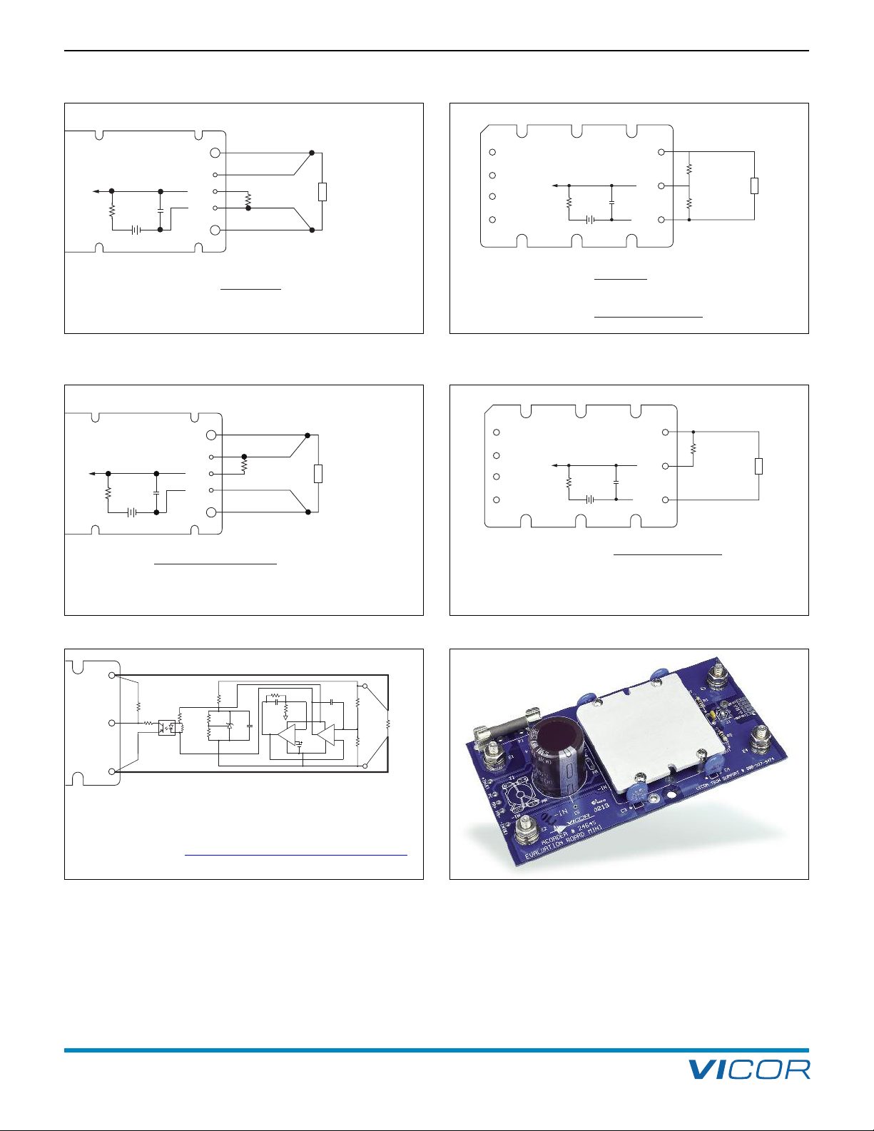
Trimming resistor calculators are available on Vicor’s web
site at http://www.vicorpower.com/powerbench. (Figure
2–16)
Resistor values can be calculated for fixed trim up, fixed
trim down, and for variable trim up or down. In addition
to trimming information, the web also includes design
tips, applications circuits, EMC suggestions, thermal
design guidelines and PDF data sheets for all Vicor
products. Evaluation Boards (Figure 2–15) are available
for the Maxi, Mini and Micro DC-DC converters.
Applications Engineering if the module’s output is
Change
VSC VOUT from
nominal
1.046 40.8 –15%
1.230 48.0 0%
1.353 52.8 +10%
Circuits such as op-amps and D/A converters, which
directly drive the SC pin, should be designed to limit the
applied voltage to the SC pin. It is also important to
consider voltage excursions that may occur during initialization of the external circuitry. The external circuit must
be referenced to the –S pin (–Out on Micro). See Figure
2–14 for remote sense implementation on Micro.
Maxi, Mini, Micro Design Guide Rev 4.9 vicorpower.com
Page 9 of 88
Apps. Eng. 800 927.9474 800 735.6200
Page 11
2. Control Pin Functions and Applications
+OUT
+S
SC
–S
–OUT
R
U
Trim Up
Load
Error
Amp
1 kΩ
1
.23 V
0.033 μF
1,000 (Vout –1.2 3) Vnom
1.23 (Vout – Vnom)
RU (ohms) =
– 1,000
R
U
Trim Up
Load
E
rror
A
mp
1 kΩ
1.2 3 V
0
.033 µF
+
OUT
S
C
–OUT
+
IN
PC
PR
–IN
1,000 (Vout –1.23 ) Vnom
1.23 (Vout – Vnom)
RU (ohms) =
– 1,000
++
––
++
––
R1
R2
U1
R3
2.55 k
R4
R5
1.00 k
U2
TLV431
C1
R7 21.0 k
C2
0.22 µF
R8
4.02 k
C3
R9
R
10
1.24 k
U3
LM10
+S
–S
+Out
SC
–Out
R Load
PS2701
R11
36.5 k
R6
1.65 k
470 pF
200 mV
Vcc
Gnd
Load
+
OUT
+S
SC
–S
–OUT
R
D
Trim Down
Error
Amp
1 kΩ
1.2 3 V
0
.033 μF
1,000 Vout
Vnom – Vout
R
D
(ohms) =
Load
R
D
Trim Down
Error
Amp
1
kΩ
1.2 3 V
0.033 μF
+OUT
SC
–OUT
+IN
PC
PR
–IN
1,000 Vout
Vnom – Vout
RD (ohms) =
1,000 (Vout –1.23) Vnom
1.23 (Vout – Vnom)
RU (ohms) =
– 1,000
R
U
Trim Up
or Maxi, Mini, Micro Family DC-DC Converters and Configurable Power Supplies
Design Guide & Applications Manual
F
Figure 2–12a — Output voltage trim down circuit (Maxi/Mini)
Figure 2–13a — Output voltage trim up circuit (Maxi/Mini)
Figure 2–12b — Output voltage trim down circuit (Micro)
Figure 2–13b — Output voltage trim up circuit (Micro)
• This module is designed for point of load regulation, where remote sensing
is not required. Active voltage drop compensator, as shown here, may be
used in applications with significant distribution losses.
Please consult with the
for additional information.
Figure 2–14 — Voltage drop compensation (Micro).
Maxi, Mini, Micro Design Guide Rev 4.9 vicorpower.com
Page 10 of 88
Micro Family Isolated Remote Sense Application Note
Apps. Eng. 800 927.9474 800 735.6200
Figure 2–15 — Evaluation Boards; Available for Maxi, Mini and Micro
Family DC-DC converters
Page 12
Design Guide & Applications Manual
or Maxi, Mini, Micro Family DC-DC Converters and Configurable Power Supplies
F
2. Control Pin Functions and Applications
EVALUATION BOARDS
• Three styles: Maxi, Mini or Micro
• Short pin and Long pin compatible
• Easy I / O and control connections
• Includes fusing and capacitors
• Can be paralleled for higher power arrays
DESCRIPTION PART NUMBER
Maxi board style 24644R
Mini board style 24645R
Micro board style 24646R
Figure 2–16 — Online trim calculator
Maxi, Mini, Micro Design Guide Rev 4.9 vicorpower.com
Page 11 of 88
Apps. Eng. 800 927.9474 800 735.6200
Page 13

3. Design Requirements
SAFETY CONSIDERATIONS
or Maxi, Mini, Micro Family DC-DC Converters and Configurable Power Supplies
F
Design Guide & Applications Manual
using. Safety agency conditions of acceptability require
F
that the module positive (+) Input terminal be fused and
the baseplate of the converter be connected to earth
ground. The following table lists the acceptable fuse types
nd current rating for the Maxi, Mini, Micro Family of
a
DC-DC converters. Safety Certifications on the Vicor web
site should always be consulted for the latest fusing
requirements.
Acceptable Fuse Types and Current Rating for the Maxi, Mini, Micro Family of Converters
Package Size Input Voltage Output Voltage Output Power Required Fuse
Maxi (A) 375 2 160 Bussmann PC-Tron 5A
Maxi (A) 375 3.3 264 / 200 Bussmann PC-Tron 5A
Maxi (A) 375 5, 8 400 / 300 Bussmann PC-Tron 5A
Maxi (A) 375 12, 15, 24, 28, 32, 36, 48, 54 600 / 400 Bussmann PC-Tron 5A
Mini (B) 375 2 100 Bussmann PC-Tron 5A
Mini (B) 375 3.3 150 / 100 Bussmann PC-Tron 5A
Mini (B) 375 5, 8 200 / 150 Bussmann PC-Tron 5A
Mini (B) 375 12, 15, 24, 28, 36, 48 300 / 200 Bussmann PC-Tron 5A
Micro (C) 375 2 50 Bussmann PC-Tron 3A
Micro (C) 375 3.3 75 / 50 Bussmann PC-Tron 3A
Micro (C) 375 5, 8 100 / 50 Bussmann PC-Tron 3A
Micro (C) 375 12, 15, 24, 28, 36, 48 150 / 75 Bussmann PC-Tron 3A
Maxi (A) 300 2 160 Bussmann PC-Tron 5A
Maxi (A) 300 3.3 264 / 200 Bussmann PC-Tron 5A
Maxi (A) 300 5, 8 400 / 300 Bussmann PC-Tron 5A
Maxi (A) 300 12, 15, 24, 28, 36, 48 500 / 400 Bussmann PC-Tron 5A
Mini (B) 300 2 100 Bussmann PC-Tron 5A
Mini (B) 300 3.3 150 / 100 Bussmann PC-Tron 5A
Mini (B) 300 5, 8 200 / 150 Bussmann PC-Tron 5A
Mini (B) 300 12, 15, 24, 28, 36, 48 250 / 150 Bussmann PC-Tron 5A
Micro (C) 300 2 50 Bussmann PC-Tron 3A
Micro (C) 300 3.3 75 / 50 Bussmann PC-Tron 3A
Micro (C) 300 5, 8 100 / 50 Bussmann PC-Tron 3A
Micro (C) 300 12, 15, 24, 28, 36, 48 150 / 75 Bussmann PC-Tron 3A
Maxi (A) 150 3.3 264 / 200 Bussmann ABC-8
Maxi (A) 150 5, 8 400 / 300 Bussmann ABC-8
Maxi (A) 150 12, 15, 24, 28, 36, 48 500 / 400 Bussmann ABC-8
Mini (B) 150 3.3 150 / 100 Bussmann PC-Tron 5A
Mini (B) 150 5, 8 200 / 150 Bussmann PC-Tron 5A
Mini (B) 150 12, 15, 24, 28, 36, 48 250 / 150 Bussmann PC-Tron 5A
Micro (C) 150 3.3 75 Bussmann PC-Tron 3A
Micro (C) 150 5, 8 100 Bussmann PC-Tron 3A
Micro (C) 150 12, 15, 24, 28, 36, 48 150 Bussmann PC-Tron 3A
Maxi (A) 110 3.3 200 / 150 Bussmann ABC-8
Maxi (A) 110 5, 8 300 / 200 Bussmann ABC-8
Maxi (A) 110 12, 15, 24, 28, 36, 48 400 / 300 Bussmann ABC-8
Mini (B) 110 3.3 100 / 75 Bussmann PC-Tron 5A
Mini (B) 110 5, 8 150 / 100 Bussmann PC-Tron 5A
Mini (B) 110 12, 15, 24, 28, 36, 48 200 / 150 Bussmann PC-Tron 5A
Micro (C) 110 3.3 50 Bussmann PC-Tron 3A
Micro (C) 110 5, 8 75 Bussmann PC-Tron 3A
Micro (C) 110 12, 15, 24, 28, 36, 48 100 Bussmann PC-Tron 3A
Maxi, Mini, Micro Design Guide Rev 4.9 vicorpower.com
Page 12 of 88
Apps. Eng. 800 927.9474 800 735.6200
Page 14

Design Guide & Applications Manual
or Maxi, Mini, Micro Family DC-DC Converters and Configurable Power Supplies
F
3. Design Requirements
Acceptable Fuse Types and Current Rating for the Maxi, Mini, Micro Family of Converters
Package Size Input Voltage Output Voltage Output Power Required Fuse
Maxi (A) 72 3.3 264 Bussmann ABC-12
Maxi (A) 72 5, 8 300 Bussmann ABC-12
Maxi (A) 72 12, 15, 24, 28, 36, 48 400 Bussmann ABC-12
Mini (B) 72 3.3 100 Bussmann ABC-8
Mini (B) 72 5, 8 150 Bussmann ABC-8
Mini (B) 72 12, 15, 24, 28, 36, 48 250 Bussmann ABC-8
Micro (C) 72 3.3 75 Bussmann PC-Tron 5A
Micro (C) 72 5, 8 100 Bussmann PC-Tron 5A
Micro (C) 72 12, 15, 24, 28, 36, 48 150 Bussmann PC-Tron 5A
Maxi (A) 48 3.3 264 Bussmann ABC-10
Maxi (A) 48 5, 8 400 Bussmann ABC-15
Maxi (A) 48 12, 15, 24, 28, 36, 48 500 Bussmann ABC-20
Mini (B) 48 2 100 Bussmann ABC-8
Mini (B) 48 3.3 150 Bussmann ABC-8
Mini (B) 48 5, 8 200 Bussmann ABC-10
Mini (B) 48 12, 15, 24, 28, 36, 48 250 Bussmann ABC-10
Micro (C) 48 2 50 Bussmann PC-Tron 5A
Micro (C) 48 3.3 75 / 50 Bussmann PC-Tron 5A
Micro (C) 48 5, 8 100 / 75 / 50 Bussmann ABC-8
Micro (C) 48 12, 15, 24, 28, 36, 48 150 / 75 Bussmann ABC-8
Maxi (A) 28 3.3 150 Bussmann ABC-25
Maxi (A) 28 5 175 Bussmann ABC-25
Maxi (A) 28 6.5, 8, 12, 15, 24, 28, 36, 48 200 Bussmann ABC-30
Mini (B) 28 3.3 75 Bussmann ABC-15
Mini (B) 28 5 75 Bussmann ABC-15
Mini (B) 28 12, 15, 24, 28, 36, 48 150 Bussmann ABC-15
Micro (C) 28 3.3 50 Bussmann ABC- 8
Micro (C) 28 5 50 Bussmann ABC-10
Micro (C) 28 12, 15, 24, 28, 36, 48 100 Bussmann ABC-10
Maxi (A) 24 3.3 264 / 200 Bussmann ABC-25
Maxi (A) 24 5, 8, 12, 15, 24, 28, 36, 48 400 / 300 Bussmann ABC-30
Mini (B) 24 3.3 150 / 100 Bussmann ABC-15
Mini (B) 24 5, 8, 12, 15, 24, 28, 36, 48 200 / 150 Bussmann ABC-15
Micro (C) 24 3.3 75 / 50 Bussmann ABC-8
Micro (C) 24 5, 8, 12, 15, 24, 28, 36, 48 100 / 50 Bussmann ABC-10
Maxi, Mini, Micro Design Guide Rev 4.9 vicorpower.com
Page 13 of 88
Apps. Eng. 800 927.9474 800 735.6200
Page 15

3. Design Requirements
or Maxi, Mini, Micro Family DC-DC Converters and Configurable Power Supplies
F
Design Guide & Applications Manual
The fuse must be in series with the positive (+) Input lead.
Fusing the negative (–) Input lead does not provide adequate
protection since the PR and PC terminals of the converter
re referenced to the –Input. If a fuse located in the
a
–Input lead were to open, the PR and PC terminals could
ise to the potential of the +Input. This may damage any
r
converter or circuitry connected to these pins. The fuse
should not be located in an area with a high ambient
temperature as this will lower the current rating of the fuse.
THERMAL AND VOLTAGE HAZARDS
Vicor component power products are intended to be used
within protective enclosures. Vicor DC-DC converters work
effectively at baseplate temperatures, which could be
harmful if contacted directly. Voltages and high currents
(energy hazard) present at the terminals and circuitry
connected to them may pose a safety hazard if contacted
or if stray current paths develop. Systems with removable
circuit cards or covers which may expose the converter(s)
or circuitry connected to the converters, should have proper
guarding to avoid hazardous conditions.
The module pins are intended for PCB mounting either by
wave soldering to a PCB or by insertion into one of the
recommended PCB socket solutions. Use of discrete wire
soldered directly to the pins may cause intermittent or
permanent damage to the module; therefore, it is not recommended as a reliable interconnection scheme for production as a final released product. In addition, modules
that have been soldered into printed circuit boards and
have subsequently been removed should not be reused.
PC PIN
The PC pin should be used only to; disable the module,
provide a bias to input referenced circuitry or communicate
status of the module. The PC pin is referenced to the –Input
pin. All circuits that connect to the PC pin must use the
–Input as the reference. Do not break the connection
between the –Input and the circuitry connected to the
PC pin or damage to the module will result. Additional
requirements include:
HIGH-POWER ARRAYS AND PR PIN
To simplify the implementation of large arrays, a subset of
modules within the parallel array should be configured as
boosters (listeners) by connecting the SC pin to the –S pin.
Modules, which are configured as boosters, cannot assume
the role of drivers (talkers) for N+M redundant arrays.
Modules configured as boosters may be locally sensed.
Each module within the parallel array must be properly
bypassed with capacitors. Film or ceramic types should be
used across the input of the module and between each
input lead and the baseplate. Modules having input
sources, which are not connected to SELV sources, should
use X-capacitors across the input and Y-capacitors from
each input power pin to the baseplate. When in doubt
about capacitor safety approvals, always consult with the
governing safety regulatory agency or Vicor Applications
Engineering.
A maximum of 12 modules may be directly connected in
parallel. Please contact Vicor Applications Engineering for
assistance with larger arrays.
The PR pin is referenced to the –In pin; therefore, all
modules within the array must have a common lowimpedance connection between each –In pin. Special
precautions are necessary if a PCB is not used for interconnection of modules, because the wiring impedance
can be significant. Do not allow the connection between
the –In pin and the –In bus to become disconnected as
damage to the module will result.
Coupling transformers should be used to transmit the PR
pulse if long distances between each module are anticipated or if the interconnection impedance of the –In leads
is high or questionable. PR coupling transformer(s) should
be used if the PR pulse exits the PCB. For example, an
array constructed of multiple circuit cards plugged into a
backplane with a number of converters on each card
should have a PR coupling transformer at the entry point
of each card; however, no coupling transformer would be
required between each converter on the card of three or
less converters on a single PCB. Do not externally drive the
PR pin, connection to this pin is limited to Vicor module
application only.
• Circuits that derive their power from the PC pin must
not exceed 1.5 mA.
• Do not drive the PC pin with external circuitry.
• Do not attempt to control the output of the converter
by PWM pulsing of the PC pin, or exceed a repetitive
on / off rate of 1 Hz.
For applications where the converter will be disabled on a
INPUT SOURCE IMPEDANCE
The impedance of the source feeding the input of the
module directly affects both the stability and transient
response of the module. In general, the source impedance
should be lower than the input impedance of the module
by a factor of ten, from DC to 50 kHz.
regular basis or where capacitance is added to this pin,
please contact Vicor
Maxi, Mini, Micro Design Guide Rev 4.9 vicorpower.com
Page 14 of 88
Applications Engineering.
Apps. Eng. 800 927.9474 800 735.6200
Page 16

Design Guide & Applications Manual
or Maxi, Mini, Micro Family DC-DC Converters and Configurable Power Supplies
F
3. Design Requirements
To calculate the required source impedance, use the
following formula:
Z = 0.1(VLL)2/ Pin
where: Z is required input impedance
s the low line input voltage
VLLi
P
in is the input power of the module
Filters, which precede the module, should be well damped
to prevent ringing when the input voltage is applied or
the load on the output of the module is abruptly changed.
INPUT TRANSIENTS AND SURGES
The voltage applied to the input of the module must not
exceed the ratings outlined in the data sheet. Protection
devices such as Zener diodes and MOVs should be used
to protect the module from short-duration transients.
These shunt protection devices are effective only if the
source impedance is high relative to the impedance of
the protection device when it is conducting. For voltage
surges where the abnormal voltage is present for a long
period of time, shunt protection devices can easily be
damaged by the power dissipated. For this type of
condition, a voltage limiter in series with the input of
the module may be the best solution. Vicor Applications
Engineering can assist in recommending the appropriate
type of protection for the module.
NOTE: Do not allow the rate of change of the
input voltage to exceed 10 V/µs for any input
voltage deviation.
SENSE LEADS (Mini and Maxi only)
The sense leads of the module must always terminate
either directly to the output pins (local sense) or at the
load (remote sense). When remote sense is used, the
output wiring impedance in combination with the load
impedance can cause significant loss of phase margin and
result in oscillation and possible damage to the module,
poor transient response, or activation of the output
overvoltage protection. Long sense leads may require a
compensation circuit for stability.
Protection circuitry is required if the possibility of reversed
sense leads can occur. Please contact Vicor Applications
Engineering for specific recommendations.
Do not
exceed 1 V between –S and –Out leads. This is
an important consideration if the converter is used in a
Hot-Swap application. ORing diodes, if used, should be
located in the +Output lead to avoid exceeding this rating.
OUTPUT CONNECTIONS
For systems designed to charge batteries, subject the
module output to dynamic loading, or loads that have
large reactive components, please contact Vicor
Applications Engineering to discuss your application
in detail.
Do not externally drive the output of the module 10%
above its nominal setpoint voltage.
Modules, that are used to charge batteries should be
applied with a diode in series with the output of the
module. The charge current must be externally controlled
to ensure that the module is not operated in excess of its
power or current rating.
Current-carrying conductors should be sized to minimize
voltage drops.
Do not
use output ORing diodes with parallel arrays of
the Micro Family converters.
Output Overvoltage Protection (OVP). The OVP detection
circuitry within the converter is highly resistant to false
tripping. For the converter to shut down due to an OVP
condition two conditions must be satisfied (logical AND);
1. The voltage at the output terminals must be greater
than the OVP set point.
2. The secondary control IC within the converter must be
requesting a power conversion cycle from the internal
primary control IC.
By using this logic, false tripping of individual converters
due to externally induced OVP conditions such as load
dumps or, being driven by external voltage sources at the
output terminals is minimized. The user should not test
the OVP circuit by back driving the output terminals or by
any other means as the OVP circuitry is fully tested as part
of the inline manufacturing process.
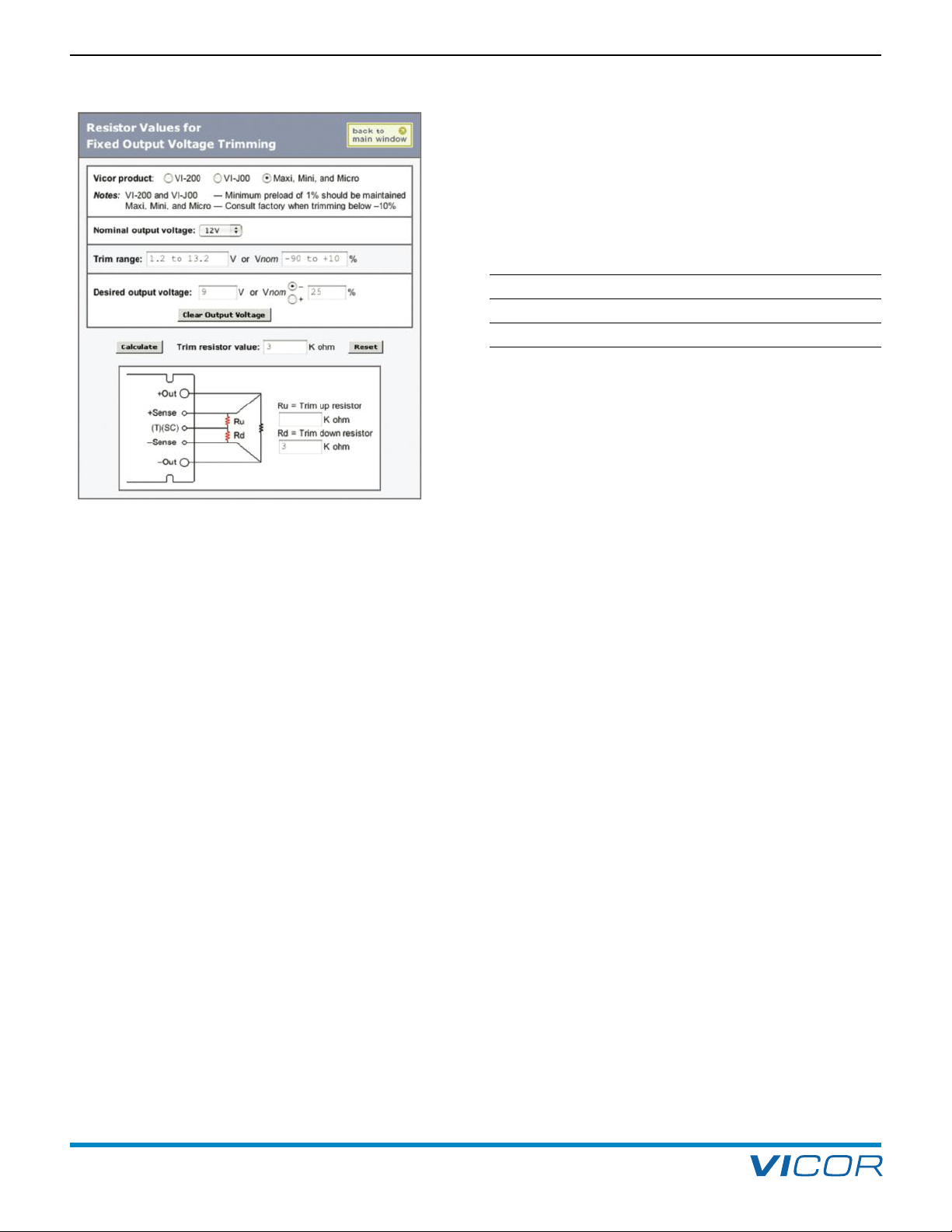
OVERCURRENT PROTECTION
The Maxi, Mini, Micro converters incorporate a straightline type current limit. (Figure 3–1) As output current is
increased beyond Imax, the output voltage remains
constant and within its specified limits up to a point, IKNEE,
which is typically 5 – 25% greater than rated current,
Imax. Beyond IKNEE, the output voltage falls to Ishortcircuit.
Typically, modules will automatically recover after the overcurrent condition is removed.
Do not
exceed the rated power of the converter. The total
of the power consumed by the load plus the power lost in
conductors from the converter to the load must be less
than the output power rating of the converter.
Maxi, Mini, Micro Design Guide Rev 4.9 vicorpower.com
Page 15 of 88
Apps. Eng. 800 927.9474 800 735.6200
Page 17
3. Design Requirements
V
out
I
K
NEE
I
M
AX
I
S
HORT CIRCUIT
I
out
Figure 3–1 — Typical Maxi, Mini, Micro current limiting
MAXIMUM OUTPUT CAPACITANCE
In general, adding external capacitance to the Maxi, Mini,
and Micro’s output is not required. However, it is often
common practice with power supply designs to add external
capacitance to the converter output for attenuation of
output ripple and / or improving dynamic load performance.
The Maxi, Mini, Micro converters typically have a faster
response to dynamic loads than other power solutions;
hence, external capacitors may not be necessary. In addition,
the output ripple and noise specification listed on the data
sheet may be acceptable for many applications.
A general equation for determining the maximum recommended output capacitance is as follows:
Pout
C(farad) =Vout
(400x10
Vout
-
6
)
or Maxi, Mini, Micro Family DC-DC Converters and Configurable Power Supplies
F
Design Guide & Applications Manual
ABSOLUTE MAXIMUM RATINGS
Please consult the latest module data sheets available on
the Vicor website for maximum ratings concerning pin-topin voltages, isolation, temperature, and mechanical ratings.
GROUNDING OF BASEPLATE AND REFERENCING
OF INPUT AND OUTPUT TERMINALS
The baseplate of the converter should always be connected
to earth ground. If for any reason this is not possible in
your application please consult with Vicor Applications
Engineering for acceptable alternatives for your application.
The input and output leads of the converter should be
referenced to the baseplate at some point to avoid stray
voltages. For offline applications the input leads are often
referenced to earth ground at the AC source ahead of the
bridge rectifier. Either + or –Output terminal may be
referenced to earth ground and the baseplate. “Floating”
inputs or outputs should at a minimum have a highresistance divider to bleed off stray charges to avoid
damage to the insulation system.
HIGH FREQUENCY BYPASSING
All Vicor converters must be bypassed for proper operation.
(Figure 3–2) The minimum complement of high-frequency
bypass capacitors must consist of the following:
• 0.2 µF ceramic or film type connected between
+In and –In.
• 4.7 nF Y-capacitor between +In and baseplate
and –In and baseplate.
• 10 nF ceramic or film capacitor between +Out and
baseplate and –Out and baseplate.
where: Pout is the output power of the converter
out is the nominal output voltage of the converter
V
All applications utilizing Maxi, Mini, Micro converters
should be properly bypassed, even if no EMC standards
need to be met. Bypass Vin and Vout pins to each module
baseplate as shown in Figure 3–2. Lead length should
The capacitance value is not the absolute maximum value,
but the value for which general application of the converter
can be deemed appropriate. Testing will be required to
ensure that the module is stable if this value is exceeded.
Approximately 10X the value calculated will cause the
converter to go into current limit at turn-on.
CAUTION:
If exceeding this value, it is recommended
that Vicor Applications Engineering be consulted.
be as short as possible. Recommended values vary
depending on the front end, if any, that is used with the
modules, and are indicated on the appropriate data sheet
or application note. In most applications, C1 is a 4,700 pF
Y-capacitor (Vicor P/N 01000) carrying the appropriate
safety agency approval; C2 is a 4,700 pF Y-capacitor (Vicor
P/N 01000) or a 0.01 µF ceramic capacitor rated at 500 V.
In PC board applications, each of these components is
typically small enough to fit under the module baseplate
flange. For PCB mounting of the module. Please refer to
Figures 3–3 and 3–4.
Maxi, Mini, Micro Design Guide Rev 4.9 vicorpower.com
Page 16 of 88
Apps. Eng. 800 927.9474 800 735.6200
Page 18
Design Guide & Applications Manual
0. 53
Ch as si s
0. 46
Onboard Mount
Cross-sectional view of pins
and mounting hardware
Inboard Mount
Cross-sectional view of pins
and mounting hardware.
Exploded View Exploded View
P/ N 20 265 Th er mM ate
Ex . V3 00 C1 2M75 BL
(L on g Sol de r Pin ,
Sl ot te d B as ep lat e)
P/ N 18 157 S ta ndo ff K it
PC B th ick nes s is
0. 06 2
" (
1. 5m m)
Tap ped # 4– 40
sc rew h ol e
Pa d a nd pl at ed th ro ughho le c onn ec te d t o
ch as si s g roun d p la ne
P/ N 20 265 Th er mM ate
Ex . V3 00 C1 2M75 B
(S ho r t Sol de r Pin,
Sl ot te d B as ep lat e)
P/ N 18 151 S ta ndo ff K it
0. 06 2
" (1.5mm) PCB with
aperture to allow belly
of
th e mo dul e to re ce ss int o b oa rd
Tap ped # 4– 40
sc rew h ol e
Pa d a nd pl at ed th ro ughho le c onn ec te d t o
ch as si s g roun d p la ne
13 ,5m m
11 ,7 mm
’
’
’’
+OUT
+IN
–IN
–OUT
Maxi, Mini, Micro
D
C-DC Converter
C1a
C1b
C2a
C2b
CI
N
Baseplate grounded
Standoffs also provide necessary
mechanical support in order to
prevent mechanical stresses from
damaging the module during shock / vibration.
Standoff sitting on pad / plated through-hole
that is connected to the chassis
ground plane within the PCB.
Female-female standoffs are
s
hown, however standoffs are
also available in male-female versions.
or Maxi, Mini, Micro Family DC-DC Converters and Configurable Power Supplies
F
3. Design Requirements
Figure 3–2 — Minimum recommended bypassing for Maxi, Mini,
and Micro; Keep all leads short.
Figure 3–3 — Recommended mounting method using standoffs
Figure 3–4 — Onboard vs. inboard mounting of (1/4 brick) Micro with slotted baseplate
Maxi, Mini, Micro Design Guide Rev 4.9 vicorpower.com
Page 17 of 88
Apps. Eng. 800 927.9474 800 735.6200
Page 19

4. EMC Considerations
FILTERING AND TRANSIENT PROTECTION
or Maxi, Mini, Micro Family DC-DC Converters and Configurable Power Supplies
F
Design Guide & Applications Manual
ll switching power supplies generate potentially interfer-
A
ing signals as a result of high-frequency, high-power
switching. The Vicor power converter topology, to a large
extent, addresses the problem at the source by the use of
a quasi-resonant, zero-current switching (ZCS) and zerovoltage switching (ZVS) topology. The switching current
waveform is a half sine wave that generates far less
conducted and radiated noise in both frequency spectrum
and magnitude. EMI filtering, if properly designed and
implemented, reduce the magnitude of conducted noise
an additional 40 – 60 dB, and as a result, the noise radiated
by the power conductors is reduced proportionally.
BASIC GUIDELINES FOR SUCCESSFUL EMI FILTERING
1. Keep current loops small. The ability of a conductor to
couple energy by induction and radiation is reduced
accordingly.
2. For conductor pairs, use wide (low Z) copper traces
aligned above and below each other.
3. Locate filters at the source of interference; i.e., close
to the power converter(s).
4. Filter component values should be chosen with
consideration given to the desired frequency range of
attenuation. For example, capacitors are self-resonant
at a certain frequency, beyond which they look inductive.
Keep bypass capacitor leads as short as possible.
5. Locate components on the PCB with consideration
given to proximity of noise sources to potentially
susceptible circuits. For example, the FIAM is an input
line filter module that has been optimized for use
with Maxi, Mini, and Micro DC-DC converters. When
used in conjunction with the recommended external
components and layout, it will significantly reduce the
differential and common-mode noise returned to the
power source. The FIAM meets the requirements of
EN55022 “B”, FCC “B”, and Bellcore GR-001089CORE, Issue 2 when used with any combination of
Maxi, Mini, and Micro converters up to the FIAM’s
maximum rated current.
onducted noise on the input power lines can occur as
C
either differential-mode or common-mode noise currents.
Differential-mode noise, largely at low frequencies, appears
across the input conductors at the fundamental switching
frequency and its harmonics. Common-mode noise, which
has mostly high-frequency content, is measured between
the converter’s input conductors and ground.
The Vicor power converter being an electronic device may
be susceptible to high levels of conducted or radiated
emissions. It is the responsibility of the user to assess
testing protocols in order to determine applicability of the
converter in the intended application.
DC-DC converter inputs and outputs must be properly
bypassed, to system chassis or earth. Bypass Vin and Vout
pins to each DC-DC module baseplate. Capacitor lead
length must be as short as possible. (Figure 4–1)
EMI filtering can be application dependent. A packaged
filter module may not always be the appropriate solution,
and the general practice of bypassing Vin and Vout may
not produce optimal results. You may have to adjust the
values depending on the severity of common-mode and
differential-mode noise. (Figures 4–2 and 4–3)
Input transient suppression should be used in applications
where source transients may be induced by load changes,
blown fuses, etc. The level of transient suppression
required will depend on the expected severity of the transients. A Zener diode, TRANSORB™, or MOV will provide
transient suppression, act as a voltage clamp for DC input
spikes, and provide reverse input voltage protection. The
device voltage rating should be chosen above high-line
voltage limits to avoid conducting during normal
operation which would result in overheating.
Module shields that provide shielding around the belly
(label side) of the Maxi, Mini, Micro are also available for
applications that are highly noise sensitive. Module shield
information is available on the Vicor website, see links
provided, on the following page.
NOTE:
Acoustic Noise. Audible noise may be emitted
from the module under no load, light load, or
dynamic loading conditions. This is considered
normal operation of the module.
Maxi, Mini, Micro Design Guide Rev 4.9 vicorpower.com
Page 18 of 88
Apps. Eng. 800 927.9474 800 735.6200
Page 20
Design Guide & Applications Manual
+IN
PC
PR
–IN
+OUT
+S
SC
–S
–OUT
C3*
4.7nF
C
2*
4
.7nF
F
or C1 – C5, keep leads and connections short.
C
5*
4.7nF
C4*
4.7nF
F1*
C1*
0.2µF
or Maxi, Mini, Micro Family DC-DC Converters and Configurable Power Supplies
F
4. EMC Considerations
Figure 4–1 — Recommended bypassing capacitors must be in close
proximity, i.e., have short lead length to be effective.
Figure 4–3 — V48B28H250BN with recommended bypass caps
(330 µF across input)
Module Shield Information
Module shield for Maxi with threaded or through-hole baseplate P/N 30142
http://asp.vicorpower.com/CADPDF/H7CEX3.PDF
Figure 4–2 — V48B28H250BN without bypass caps
(330 µF across input)
Module shield for Maxi with slotted baseplate P/N 30199
http://asp.vicorpower.com/CADPDF/HXE113.PDF
Module shield for Mini with threaded or through-hole baseplate P/N 30180
http://asp.vicorpower.com/CADPDF/UT55TT.PDF
Module shield for Mini with slotted baseplate P/N 30198
http://asp.vicorpower.com/CADPDF/HXE112.PDF
Module shield for Micro with threaded or through-hole baseplate P/N 30143
http://asp.vicorpower.com/CADPDF/9YRD8X.PDF
Module shield for Micro with slotted baseplate P/N 30141
Maxi, Mini, Micro Design Guide Rev 4.9 vicorpower.com
Page 19 of 88
http://asp.vicorpower.com/CADPDF/NG6SIS.PDF
Apps. Eng. 800 927.9474 800 735.6200
Page 21

5. Current Sharing In Power Arrays
or Maxi, Mini, Micro Family DC-DC Converters and Configurable Power Supplies
F
Design Guide & Applications Manual
Whenever power supplies or converters are operated in
a parallel configuration — whether for higher output
power, fault tolerance, or both — current sharing is an
mportant consideration. Most current-sharing schemes
i
employed with power converters involve either artificially
ncreasing the output impedance of the converter module
i
or actually sensing each output current, forcing all of the
currents to be equal by feedback control. In a synchronous
current-sharing scheme, however, there is no need for
having a current-sensing or current-measuring device on
each module, nor is there a need to artificially increase the
output impedance, which compromises load regulation.
WHY IS CURRENT SHARING IMPORTANT
Most paralleled power components — transistors, rectifiers,
power conversion modules, offline power supplies — will
not inherently share the load. In the case of power converters, one or more of the converters will try to assume a
disproportionate or excessive fraction of the load unless
forced current-share control is designed into the system.
One converter — typically the one with the highest output
voltage — may deliver current up to its current limit setting,
which is beyond its rated maximum. Then the voltage will
drop to the point where another converter in the array —
the one with the next highest voltage — will begin to
deliver current. All of the converters in an array may deliver
some current, but the load will be shared unequally. Built-in
current limiting may cause all or most converters to deliver
current, but the loading will remain unbalanced, and
potentially cause damage to the converters.
Consider the situation when one module in a two-module
array is providing all of the load. If it fails, the load on the
second module must go from no load to full load, during
which time the output voltage is likely to droop temporarily.
This could result in system problems, including shutdown
or reset. If both modules were sharing the load and one
failed, however, the surviving module would experience a
much less severe transient (one half to full load), and the
output voltage would be likely to experience no more
than a slight momentary droop. The dynamic response
characteristic of all forward converters, resonant or pulsewidth modulated, is degraded when the load is stepped
from zero (no load) where the output inductor current is
discontinuous.
In the same two-module array example, the module
carrying all of the load is also generating all of the heat,
resulting in a much lower mean time between failure
(MTBF) for that module. An often-quoted rule of thumb
says that for each 10°C increase in operating
temperature, average component life is cut in half. In a
current-sharing system, all of the converters or supplies
run at a lower temperature than some modules would in
a system without current sharing. As a result, all of the
modules age equally.
Current sharing, then, is important because it improves
system performance; it minimizes transient / dynamic
response and thermal problems and improves reliability. It
is an essential ingredient in most systems that use multiple
power supplies or converters for higher output power or
for fault tolerance.
CURRENT-SHARING IN POWER EXPANSION ARRAYS
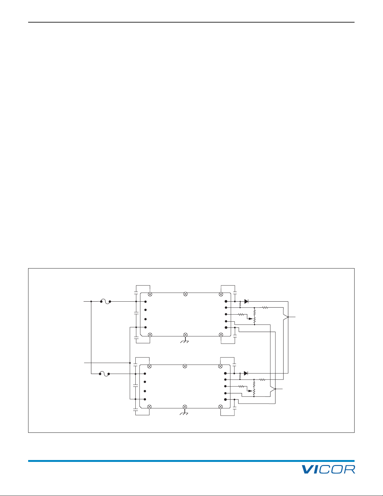
When parallel supplies or converters are used to increase
power, current sharing is achieved by a number of
approaches. One scheme simply adds resistance in series
with the load. A more practical variant of that is the
“droop-share” method, which actively causes the output
voltage to drop in response to increasing load. The two
most commonly used approaches to paralleling converters
for power expansion are the driver/booster or master/
slave arrays and analog current-share control. They appear
to be similar, but the implementation of each is quite
different. Driver/booster arrays usually contain one
intelligent module or driver, and one or more power-trainonly modules or boosters. Analog current-share control
involves paralleling two or more identical modules, each
containing intelligence.
Droop Share. The droop-share method, shown in Figure
5–1, increases the output impedance to force the currents
to be equal. It is accomplished by an error signal, which is
interjected into the control loop of the converter causing
the output voltage to operate as a function of load
current. As load current increases, output voltage
decreases. All of the modules will have approximately the
same amount of current because they are all being
summed into one node. If one supply is delivering more
current than another supply, its output voltage will be
forced down a little so that it will be delivering equal
current for an equal voltage out of that summing node.
Figure 5–1 illustrates a simple implementation of this
scheme where the voltage dropped across the ORing
diode, being proportional to current, is used to adjust the
output voltage of the associated converter.
Droop share has advantages and disadvantages. One of
the advantages is that it can work with any topology. It is
also fairly simple and inexpensive to implement. A major
drawback, though, is that it requires that the current be
sensed. A current-sensing device is needed in each of the
converters or power supplies. In addition, a small penalty
is paid in load regulation, although in many applications
this is not an issue.
Maxi, Mini, Micro Design Guide Rev 4.9 vicorpower.com
Page 20 of 88
Apps. Eng. 800 927.9474 800 735.6200
Page 22
Design Guide & Applications Manual
Return
+S
+OUT
SC
–S
–OUT
–IN
PR
PC
+IN
+S
+OUT
SC
–S
–OUT
–IN
PR
PC
+IN
DC-DC Converter
Maxi or Mini
+IN
– IN
+OUT
DC-DC Converter
Maxi or Mini
or Maxi, Mini, Micro Family DC-DC Converters and Configurable Power Supplies
F
5. Current Sharing In Power Arrays
In general, it is not recommended to mix and match converters, especially those with incompatible current-sharing
schemes. The droop-share method, however, is more
orgiving in this regard than with any of the other
f
methods. Current sharing can be achieved using arrays
onstructed from different converter models or even from
c
different suppliers with a little external circuitry.
Driver/ Booster Arrays. Most Vicor converters can
employ the driver/booster array for increased power.
(Figure 5–2) Driver/booster arrays usually contain one
intelligent module or driver, and one or more power-trainonly modules or boosters. The driver is used to set and
control output voltage, while booster modules are used
to increase output power to meet system requirements.
Driver/booster arrays of quasi-resonant converters with
identical power trains inherently current share because
the per-pulse energy of each converter is the same. If the
inputs and outputs are tied together and the units have
the same clock frequency, all modules will deliver the
same current (within component tolerances). The single
intelligent module in the array determines the transient
response, which does not change as modules are added.
Booster modules require only one connection between
units when their outputs are connected; no trimming,
adjustments, or external components are required to
achieve load sharing. The load sharing is dynamic and
usually guaranteed to be within five percent.
It is important to remember that when using boosters, the
input voltage, output voltage, and output power of the
boosters must be the same as the driver.
The advantages of driver/booster arrays are that they
have only a single control loop so there are no loop-withina-loop stability issues, and they have excellent transient
response. However, this arrangement is not fault tolerant.
If the driver module fails, the array will fail to maintain its
output voltage.
Analog Current-Share Control. Analog current-share
control, typical of PWM type converters, involves
paralleling two or more identical modules, each
containing intelligence. The circuit actively adjusts the
output voltage of each supply so that the multiple
supplies deliver equal currents. This method, however, has
a number of disadvantages. Each converter in the array
has its own voltage regulation loop, and each requires a
current sensing device and current control loop.
Analog current-share control supports a level of redundancy,
but it is susceptible to single-point failures within the
current-share bus that can, at best, defeat current sharing,
and, at worst, destroy every module in the array. The
major reason for this is the single-wire galvanic connection
between modules.
Figure 5–1 — The droop-share method artificially increases the output impedance to force the currents to be equal.
Maxi, Mini, Micro Design Guide Rev 4.9 vicorpower.com
Page 21 of 88
Apps. Eng. 800 927.9474 800 735.6200
Page 23

5. Current Sharing In Power Arrays
or Maxi, Mini, Micro Family DC-DC Converters and Configurable Power Supplies
F
Design Guide & Applications Manual
CURRENT SHARING IN FAULT TOLERANT ARRAYS
Current sharing is an essential element in fault-tolerant
arrays, and regardless of the approach, there is an
inherent additional cost incurred by the addition of at
least one redundant converter or supply.
Most applications today that require fault tolerance or
redundancy also require Hot-Swap capability to ensure
continuous system operation. Hot swappable cards must
be designed so that the operator cannot come in contact
with dangerous potentials, currents or thermal hazards. It
is also essential that when a module fails, the failure is
detected and identified by an alarm or notice to provide
service. A Hot-Swap system must ensure that during swap
out there is minimal disturbance of the power bus.
Specifically, the affected voltage bus must not drop
enough to cause errors in the system, either on the input
bus or the output bus.
N+1 Redundancy. A power supply failure can cripple an
entire system, so a redundant converter or supply can be
added to ensure that, in the event of a failure, the system
will continue to operate. Adding an extra module (N+1) to
a group of paralleled modules will significantly increase
reliability with only a modest increase in cost.
How redundant converters are implemented is determined
in part by the available space and cost requirements. Two
500 W Maxi modules, for example, could be used to
provide a 1 kW output with an additional 500 W module
for 2+1 redundancy a total of 1.5 kW in a volume of
about 16.5 in3 (270 cm3). Four 200 W half-size modules
might be used instead with a fifth 200 W module for
4+1 redundancy, a total of 1 kW and 14 in3(229 cm3).
Although the second solution uses less space, it increases
the accumulated failure rate because it employs more
converters, more ORing diodes, more monitoring circuitry,
and more assembly.
ORing diodes may be inserted in series with the +Output
of each module in a N+1 array to provide output fault
tolerance (Figure 5–1). They are important in a redundant
power system to maintain fault isolation. Without them,
a short-circuit failure in the output of one converter could
bring down the entire array. As well, fusing the input of
each converter prevents a converter input short from
compromising the entire array.
ORing diodes, however, add losses to the power system,
reducing overall efficiency (and, potentially, decreasing
reliability). To ameliorate this negative effect on efficiency,
ORing diodes should run hot, thereby reducing forward
voltage drop and improving system efficiency. Reverse
leakage current will be an issue only if the output of a
converter shorts and the diode is reverse biased. This is an
important consideration with regard to operating temperature.
Current sharing, required to ensure system reliability, can
be implemented by a multiplicity of methods. Figure 5–1,
shown earlier as an example of the droop-share method,
s also an example of N+1 redundancy using ORing diodes.
i
Synchronous Current Sharing. Synchronous current
sharing is available with Maxi, Mini, Micro converters —
converters that use the zero-current-switching and zerovoltage-switching topology. Each module has the capability to assume control of the array, that is, they constitute a
democratic array. The module that assumes command
transmits a pulse on the parallel bus to which all other
modules on the bus synchronize.
The converters use this pulse as a current-sharing signal
for power expansion and fault-tolerant applications. The
pulsed signal on the parallel bus simplifies current-sharing
control by synchronizing the high-frequency switching of
each converter. The parallel pin is a bi-directional port on
each module used to transmit and receive information
between modules. If the lead module relinquishes control,
another module in the array will transparently take
command with little or no perturbation of the output bus.
A pulsed signal gives designers the option to use capacitors (Figure 5–2) or transformers between parallel pins,
providing DC-blocked coupling. Such coupling
prevents certain failure modes internal to a single module
from affecting the other modules in the array, thus
providing an increased level of fault tolerance.
Use of a current-share bus transformer (Figure 5–3)
enables arrays of Maxi, Mini, Micro converters to current
share when they are widely separated or operated from
independent sources. Since the current-share signal is a
pulsed signal, it can be transformer coupled. Transformer
coupling this pulsed signal provides a high level of
common-mode noise immunity while maintaining SELV
isolation from the primary source. This is especially
useful when board-to-board load sharing is required
in redundant applications.
Synchronous current sharing eliminates the need for
current-sensing or current-measuring devices on each
module, and load regulation is not compromised.
Additional advantages of the synchronous current sharing
architecture includes excellent transient response, “no
loop within a loop” control problems, and, a high degree
of immunity from system noise. The availability of synchronous current sharing in democratically controlled arrays
offers power architects new opportunities to achieve
simple, non-dissipative current-share control. It provides
options that simplify current sharing and eliminates the
tradeoffs — such as the need to sense the current from
each individual module and adjust each control voltage —
as is the case with other current-sharing methods.
Maxi, Mini, Micro Design Guide Rev 4.9 vicorpower.com
Page 22 of 88
Apps. Eng. 800 927.9474 800 735.6200
Page 24
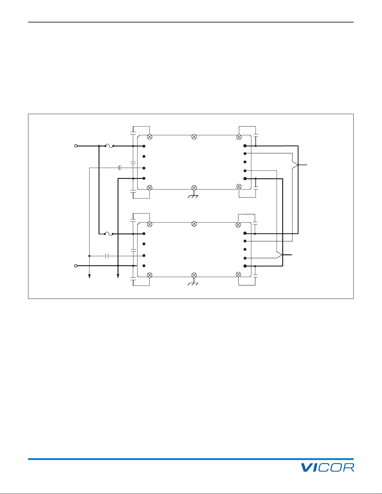
Design Guide & Applications Manual
Ground
Plane
+
S
+
OUT
S
C
–
S
–OUT
–
IN
PR
PC
+IN
+
S
+
OUT
SC
–S
–OUT
–
IN
P
R
PC
+IN
Return
DC-DC Converter
DC-DC Converter
Parallel
Bus
+V
I
N
+V
O
UT
-V
IN
or Maxi, Mini, Micro Family DC-DC Converters and Configurable Power Supplies
F
5. Current Sharing In Power Arrays
The synchronous current-sharing method applies to
quasi-resonant, frequency-modulated converters with the
necessary intelligence, such as the Vicor Maxi, Mini, Micro
amily of high-density DC-DC converters, where the energy
F
per pulse is fixed.
Finally, no matter what method is used, current sharing
reduces thermal problems, improves transient response,
and helps extend the lifetimes of all modules in an
rray. Nevertheless, all current-sharing schemes require
a
careful attention to electrical and mechanical design to
perate effectively.
o
Figure 5–2 — Synchronous power architecture simplifies current sharing control and enhances fault tolerance.
Maxi, Mini, Micro Design Guide Rev 4.9 vicorpower.com
Page 23 of 88
Apps. Eng. 800 927.9474 800 735.6200
Page 25
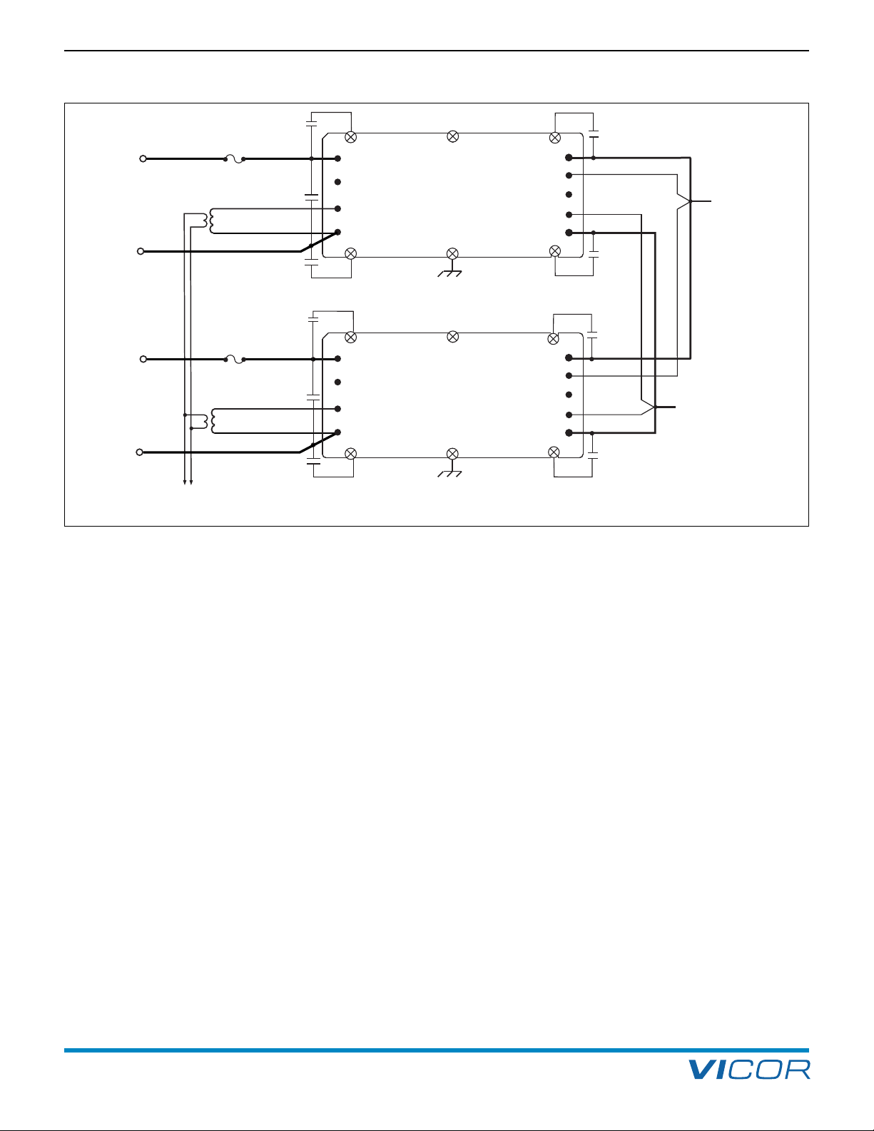
5. Current Sharing In Power Arrays
+
V
IN
Parallel
Bus
T
1
T2
-V
IN
+
V
I
N
+S
+OUT
S
C
–S
–OUT
–IN
PR
PC
+
IN
+S
+OUT
SC
–S
–OUT
–IN
PR
PC
+IN
Return
+V
OUT
-V
I
N
DC-DC Converter
DC-DC Converter
or Maxi, Mini, Micro Family DC-DC Converters and Configurable Power Supplies
Design Guide & Applications Manual
F
Figure 5–3 — Transformer-coupled interface provides load sharing and SELV isolation from the primary source.
Maxi, Mini, Micro Design Guide Rev 4.9 vicorpower.com
Page 24 of 88
Apps. Eng. 800 927.9474 800 735.6200
Page 26

Design Guide & Applications Manual
or Maxi, Mini, Micro Family DC-DC Converters and Configurable Power Supplies
F
6. Thermal Performance Information
Simplified thermal management is one of the benefits of
using Vicor converters. High operating efficiency minimizes
heat loss, and the low-profile package features an easily
ccessible, electrically isolated thermal interface surface.
a
Proper thermal management pays dividends in terms of
improved converter and system MTBFs, smaller size, and
lower product life-cycle costs. The following pages provide
guidelines for achieving effective thermal management of
Consideration should be given to the module baseplate
temperature during operation. The maximum baseplate
temperature specification for Maxi, Mini, and Micro is
00°C.
1
Enhanced module cooling can be achieved with free or
forced convection by using the appropriate heat sink. The
available Vicor heat sinks and thermal interface options
are available on the Vicor website.
Vicor converters.
The relevant nomenclature for the tabulated thermal information supplied in this section for the
Maxi, Mini, and Micro modules is defined as follows:
Tb = baseplate temperature
Ta = ambient temperature
Pout = module output power
Pin= module input power
η = module efficiency = Pout / Pin
Pdiss = module power dissipation = Pin – Pout = (1/η – 1) • Pout
Supplied thermal resistance values:
θbs = baseplate-to-heatsink thermal resistance
θba = baseplate-to-ambient thermal resistance
Basis of output power versus ambient temperature derating curves:
(Ta)max = (Tb)max – θba • Pdiss = (Tb)max – θba • (1/η – 1) • Pout
Additional Thermal Data
The following pages contain temperature derating curves.
For additional thermal data, see the following link:
http://asp.vicorpower.com/calculators/calculators.asp?calc=5
Maxi, Mini, Micro Design Guide Rev 4.9 vicorpower.com
Page 25 of 88
Apps. Eng. 800 927.9474 800 735.6200
Page 27
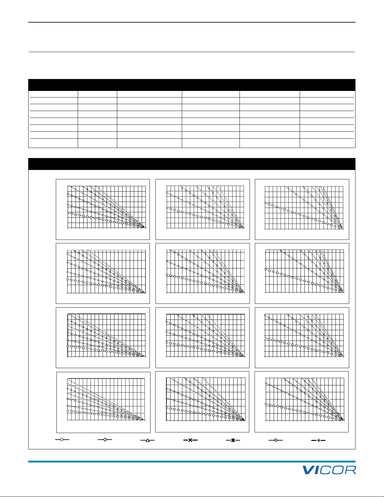
6. Thermal Performance Information
0
20
40
60
80
100
120
140
160
0
5
1015202530354045505560657075808590
95
100
Ambient Temperature (deg C)
Output Power (Watts)
0
20
40
60
80
100
120
140
160
0
5
1015202530354045505560657075808590
95
100
Ambient Temperature (deg C)
Output Power (Watts)
0
20
40
60
80
100
120
140
160
0
5
1015202530354045505560657075808590
95
100
Ambient Temperature (deg C)
Output Power (Watts)
0
50
100
150
200
250
0
5
1015202530354045505560657075808590
95
100
Ambient Temperature (deg C)
Output Power (Watts)
0
50
100
150
200
250
0
5
1015202530354045505560657075808590
95
100
Ambient Temperature (deg C)
Output Power (Watts)
0
50
100
150
200
250
0
5
1015202530354045505560657075808590
95
100
Ambient Temperature (deg C)
Output Power (Watts)
0
50
100
150
200
250
300
350
400
0
5
1015202530354045505560657075808590
95
100
Ambient Temperature (deg C)
Output Power (Watts)
0
50
100
150
200
250
300
350
400
0
5
1015202530354045505560657075808590
95
100
Ambient Temperature (deg C)
Output Power (Watts)
0
50
100
150
200
250
300
350
400
0
5
1015202530354045505560657075808590
95
100
Ambient Temperature (deg C)
Output Power (Watts)
12 - 48V Maxi Thermal Performance Curves - No Heat Sink
0
100
200
300
400
500
600
0
5
1015202530354045505560657075808590
95
100
Ambient Temperature (deg C)
Output Power (Watts)
12 - 48V Maxi Thermal Performance Curves - .4" Heat Sink
0
100
200
300
400
500
600
0
5
1015202530354045505560657075808590
95
100
Ambient Temperature (deg C)
Power Output (Watts)
12 - 48V Maxi Thermal Performance Curves - .9" Heat Sink
0
100
200
300
400
500
600
0
5
1015202530354045505560657075808590
95
100
Ambient Temperature (deg C)
Power Output (Watts)
Design Guide & Applications Manual
For Maxi, Mini, Micro Family DC-DC Converters and Configurable Power Supplies
THERMAL PERFORMANCE CURVES (Maxi)
Table Usage: The forced convection thermal impedance data shown in the tables on the next three pages assumes airflow through the heat
sink fins. Actual airflow through the fins should be verified. For purposes of heat sink calculation, assume efficiencies listed on Maxi data
sheets. Use as a design guide only. Verify final design by actual temperature measurement.
θ
Maxi
θ
bs = 0.07°C/W Baseplate 0.9'' Longitudinal Fins 0.9'' Transverse Fins 0.4'' Longitudinal Fins 0.4'' Transverse Fins
ba (Baseplate-to-Ambient Thermal Resistance Values) vs. Airflow
Free Air 4.98 2.89 2.24 3.72 3.49
200 LFM 3.23 1.30 1.02 2.14 1.53
400 LFM 2.17 0.90 0.72 1.48 1.08
600 LFM 1.73 0.72 0.60 1.10 0.87
800 LFM 1.46 0.59 0.51 0.86 0.70
1,000 LFM 1.27 0.51 0.44 0.71 0.60
1,200 LFM 1.14 0.46 0.41 0.61 0.55
Maxi Output Power vs. Ambient Temperature Derating Curves
Baseplate (No Heat Sink) 0.4'' (10,1 mm) Heat Sink 0.9'' (22,8 mm) Heat Sink
2 V
3.3 V
5 V
12 – 54 V
Maxi, Mini, Micro Design Guide Rev 4.9 vicorpower.com
Page 26 of 88
Free Air 200 LFM 400 LFM 600 LFM 800 LFM 1000 LFM 1200 LFM
Apps. Eng. 800 927.9474 800 735.6200
Page 28

Design Guide & Applications Manual
2V Mini Thermal Performance Curves - No Heat Sink
0
10
2
0
30
40
50
60
70
80
90
100
0
5
1015202530354045505560657075808590
95
100
A
mbient Temperature (deg C)
Output Power (Watts)
2V Mini Thermal Performance Curves - .4" Heat Sink
0
10
20
30
4
0
50
60
70
80
90
1
00
0
5
1015202530354045505560657075808590
95
100
Ambient Temperature (deg C)
Output Power (Watts)
2V Mini Thermal Performance Curves - .9" Heat Sink
0
1
0
20
3
0
40
50
60
70
80
90
100
0
5
1015202530354045505560657075808590
95
100
Ambient Temperature (deg C)
Output Power (Watts)
3
.3V Mini Thermal Performance Curves - No Heat Sink
0
20
40
60
80
1
00
120
140
0
5
1015202530354045505560657075808590
95
100
A
mbient Temperature (deg C)
Output Power (Watts)
3.3V Mini Thermal Performance Curves - .4" Heat Sink
0
20
4
0
60
80
1
00
1
20
1
40
0
5
1015202530354045505560657075808590
95
100
Ambient Temperature (deg C)
Output Power (Watts)
3
.3V Mini Thermal Performance Curves - .9" Heat Sink
0
2
0
40
60
80
100
120
140
0
5
1015202530354045505560657075808590
95
100
Ambient Temperature (deg C)
Output Power (Watts)
5V Mini Thermal Performance Curves - No Heat Sink
0
20
40
60
8
0
100
1
20
140
160
180
200
0
5
1015202530354045505560657075808590
95
100
Ambient Temperature (deg C)
Output Power (Watts)
5V Mini Thermal Performance Curves - .4" Heat Sink
0
20
4
0
6
0
80
100
120
140
160
180
200
0
5
1015202530354045505560657075808590
95
100
Ambient Temperature (deg C)
Output Power (Watts)
5V Mini Thermal Performance Curves - .9" Heat Sink
0
20
40
60
80
100
120
140
160
180
200
0
5
1015202530354045505560657075808590
95
100
Ambient Temperature (deg C)
Output Power (Watts)
12 - 48V Mini Thermal Performance Curves - No Heat Sink
0
50
100
150
200
250
300
0
5
1015202530354045505560657075808590
95
100
Ambient Temperature (deg C)
Output Power (Watts)
12 - 48V Mini Thermal Performance Curves - .4" Heat Sink
0
50
100
150
200
250
300
0
5
1015202530354045505560657075808590
95
100
Ambient Temperature (deg C)
Output Power (Watts)
12 - 48V Mini Thermal Performance Curves - .9" Heat Sink
0
50
100
150
200
250
300
0
5
1015202530354045505560657075808590
95
100
Ambient Temperature (deg C)
Output Power (Watts)
or Maxi, Mini, Micro Family DC-DC Converters and Configurable Power Supplies
F
6. Thermal Performance Information
THERMAL PERFORMANCE CURVES (Mini)
Table Usage: The forced convection thermal impedance data shown in the tables on the next three pages assumes airflow through the heat
sink fins. Actual airflow through the fins should be verified. For purposes of heat sink calculation, assume efficiencies listed on Mini data
sheets. Use as a design guide only. Verify final design by actual temperature measurement.
θ
Mini
ba (Baseplate-to-Ambient Thermal Resistance Values) vs. Airflow
θ
bs = 0.14°C/W Baseplate 0.9'' Longitudinal Fins 0.9'' Transverse Fins 0.4'' Longitudinal Fins 0.4'' Transverse Fins
Free Air 7.94 4.10 3.93 6.28 6.34
200 LFM 4.50 1.72 1.93 2.81 3.00
400 LFM 3.20 1.26 1.38 1.98 2.09
600 LFM 2.52 1.02 1.06 1.55 1.59
800 LFM 2.15 0.86 0.89 1.24 1.31
1,000 LFM 1.89 0.75 0.77 1.05 1.11
1,200 LFM 1.69 0.68 0.70 0.94 0.99
Mini Output Power vs. Ambient Temperature Derating Curves
Baseplate (No Heat Sink) 0.4'' (10,1 mm) Heat Sink 0.9'' (22,8 mm) Heat Sink
2 V
3.3 V
5 V
12 – 54 V
Maxi, Mini, Micro Design Guide Rev 4.9 vicorpower.com
Page 27 of 88
Free Air 200 LFM 400 LFM 600 LFM 800 LFM 1000 LFM 1200 LFM
Apps. Eng. 800 927.9474 800 735.6200
Page 29

6. Thermal Performance Information
2V Micro Thermal Performance Curves - No Heat Sink
0
5
10
15
20
25
3
0
35
4
0
45
50
0
5
1015202530354045505560657075808590
95
100
A
mbient Temperature (deg C)
Output Power (Watts)
2V Micro Thermal Performance Curves - .4" Heat Sink
0
5
10
15
20
25
30
35
40
45
50
0
5
1015202530354045505560657075808590
95
100
Ambient Temperature (deg C)
Output Power (Watts)
2V Micro Thermal Performance Curves - .9" Heat Sink
0
5
1
0
1
5
20
25
30
35
40
45
50
0
5
1015202530354045505560657075808590
95
100
Ambient Temperature (deg C)
Output Power (Watts)
3.3V Micro Thermal Performance Curves - No Heat Sink
0
10
20
30
40
50
60
70
0
5
1015202530354045505560657075808590
95
100
Ambient Temperature (deg C)
Output Power (Watts)
3.3V Micro Thermal Performance Curves - .4" Heat Sink
0
10
20
30
40
50
60
70
0
5
1015202530354045505560657075808590
95
100
Ambient Temperature (deg C)
Output Power (Watts)
3
.3V Micro Thermal Performance Curves - .9 Heat Sink
0
10
20
30
40
5
0
60
70
0
5
1015202530354045505560657075808590
95
100
Ambient Temperature (deg C)
Output Power (Watts)
5V Micro Thermal Performance Curves - No Heat Sink
0
10
20
30
40
50
60
70
80
90
100
0
5
1015202530354045505560657075808590
95
100
Ambient Temperature (deg C)
Output Power (Watts)
5
V Micro Thermal Performance Curves - .4" Heat Sink
0
10
20
30
40
5
0
60
70
8
0
90
100
0
5
1015202530354045505560657075808590
95
100
A
mbient Temperature (deg C)
Output Power (Watts)
5V Micro Thermal Performance Curves - .9" Heat Sink
0
10
20
30
40
50
60
70
80
9
0
100
0
5
1015202530354045505560657075808590
95
100
Ambient Temperature (deg C)
Output Power (Watts)
12 - 48V Micro Thermal Performance Curves - No Heat Sink
0
20
40
60
80
100
120
140
0
5
1015202530354045505560657075808590
95
100
Ambient Temperature (deg C)
Output Power (Watts)
12 - 48V Micro Thermal Performance Curves - .4" Heat Sink
0
20
40
60
80
100
120
140
0
5
1015202530354045505560657075808590
95
100
Ambient Temperature (deg C)
Output Power (Watts)
12 - 48V Micro Thermal Performance Curves - .9" Heat Sink
0
20
40
60
80
100
120
140
0
5
1015202530354045505560657075808590
95
100
Ambient Temperature (deg C)
Output Power (Watts)
or Maxi, Mini, Micro Family DC-DC Converters and Configurable Power Supplies
F
Design Guide & Applications Manual
THERMAL PERFORMANCE CURVES (Micro)
Table Usage: The forced convection thermal impedance data shown in the tables on the next three pages assumes airflow through the heat
sink fins. Actual airflow through the fins should be verified. For purposes of heat sink calculation, assume efficiencies listed on Micro data
sheets. Use as a design guide only. Verify final design by actual temperature measurement.
Micro
θ
bs = 0.21°C/W Baseplate 0.9'' Longitudinal Fins 0.9'' Transverse Fins 0.4'' Longitudinal Fins 0.4'' Transverse Fins
θ
ba (Baseplate-to-Ambient Thermal Resistance Values) vs. Airflow
Free Air 10.90 5.37 5.04 7.77 7.76
200 LFM 6.90 2.51 2.31 3.87 3.58
400 LFM 4.78 1.79 1.68 2.68 2.52
600 LFM 3.74 1.42 1.31 2.13 2.01
800 LFM 3.15 1.20 1.10 1.78 1.67
1,000 LFM 2.79 1.06 0.97 1.48 1.45
1,200 LFM 2.49 0.93 0.88 1.32 1.29
Micro Output Power vs. Ambient Temperature Derating Curves
Baseplate (No Heat Sink) 0.4'' (10,1 mm) Heat Sink 0.9'' (22,8 mm) Heat Sink
2 V
3.3 V
5 V
12 – 54 V
Maxi, Mini, Micro Design Guide Rev 4.9 vicorpower.com
Page 28 of 88
Free Air 200 LFM 400 LFM 600 LFM 800 LFM 1000 LFM 1200 LFM
Apps. Eng. 800 927.9474 800 735.6200
Page 30

Design Guide & Applications Manual
5V Mini Thermal Performance Curves - .9" Heat Sink
0
20
40
60
80
100
120
140
160
180
200
0
5
1015202530354045505560657075808590
95
100
Ambient Temperature (deg C)
Output Power (Watts)
or Maxi, Mini, Micro Family DC-DC Converters and Configurable Power Supplies
F
Typical Examples — Thermal Equations (Maxi, Mini, Micro)
EXAMPLE 1
etermine the maximum output power for a Maxi module without a heat sink delivering 5 V in 400 LFM
D
airflow at a maximum ambient temperature of 40ºC.
6. Thermal Performance Information
Maximum output power = (T
Tb
= 100ºC
ax
m
Ta
= 40ºC
max
b
– Ta
ax
m
)/[θba • (1/η – 1)]
ax
m
For Maxi module without a heat sink @ 400 LFM, θba = 2.17ºC/W
For the 5 V Maxi module the typical value for η = 0.83
Maximum output power = (100 – 40) / [2.17 (1/0.83 – 1)] ~135 W
Or, the same answer could be obtained by using the output power versus ambient temperature derating
curves for the Maxi modules.
For the case with no heat sink the baseplate chart for the 5 V module would be used. At a 40ºC ambient
and 400 LFM airflow this chart indicates a maximum output power of approximately 135 W.
For full output power of 400 W the required thermal resistance is;
θba = (100 – 40) / [400 (1/0.83 – 1)] = 0.73ºC/W
What size heat sink would be necessary to operate at full output power (400 W) under the same conditions?
From the θba versus airflow charts for the Maxi, the thermal resistance at 400 LFM airflow requires the use of
a 0.9"(22,8 mm) transverse fin heat sink.
EXAMPLE 2
Determine the maximum ambient for a Mini module with a 0.9” (22,8 mm) heat sink in 400 LFM of airflow
delivering 200 W at 5 V.
From the output power versus ambient temperature chart for the 5 Vout Mini with a 0.9’’ (22,8 mm) heat
sink, the 200 W at 400 LFM data point results in a Ta
Maxi, Mini, Micro Design Guide Rev 4.9 vicorpower.com
Page 29 of 88
5 V Mini with
0.9” (22,8 mm)
heat sink
of approximately 48ºC.
max
Apps. Eng. 800 927.9474 800 735.6200
Page 31

6. Thermal Performance Information
or Maxi, Mini, Micro Family DC-DC Converters and Configurable Power Supplies
F
Design Guide & Applications Manual
THERMAL MANAGEMENT ACCESSORIES (All parts are RoHS compliant unless otherwise noted)
axi Heat Sinks Mini Heat Sinks Micro Heat Sinks
M
Threaded Through Hole Threaded Through Hole Threaded Through Hole
0.4" (10,1 mm) Fin 0.4" (10,1 mm) Fin 0.4" (10,1 mm) Fin 0.4" (10,1 mm) Fin 0.4" (10,1 mm) Fin 0.4" (10,1 mm) Fin
P/N 30482 P/N 30718 P/N 32188 P/N 30195 P/N 32174 P/N 30719
0.9" (22,8 mm) Fin 0.9" (22,8 mm) Fin 0.9" (22,8 mm) Fin 0.9" (22,8 mm) Fin 0.9" (22,8 mm) Fin 0.9" (22,8 mm) Fin
P/N 30188 P/N 30181 P/N 30189 P/N 30182 P/N 30190 P/N 30183
0.4" (10,1 mm) Fin 0.4" (10,1 mm) Fin 0.4" (10,1 mm) Fin 0.4" (10,1 mm) Fin 0.4" (10,1 mm) Fin 0.4" (10,1 mm) Fin
P/N 30778 P/N 30720 P/N 30184 P/N 30721 P/N 32173 P/N 30722
Transverse Fins Longitudinal Fins
0.9" (22,8 mm) Fin 0.9" (22,8 mm) Fin 0.9" (22,8 mm) Fin 0.9" (22,8 mm) Fin 0.9" (22,8 mm) Fin 0.9" (22,8 mm) Fin
P/N 30196 P/N 30723 P/N 30269 P/N 30724 P/N 30270 P/N 30725
Low-profile Side-fin Heat Sinks
Height only 0.125" (3,17 mm) above module baseplate*
0.55" (13,97 mm) 0.55" (13,97 mm) 0.55" (13,97 mm)
Side Fins Side Fins Side Fins
P/N 30096 P/N 32190 P/N 30095
See the specific products on the Vicor website for more information.
Standoffs and Screws
Bulk and single-module kits compatible
with all standard mounting configurations.
Not compatible with standoff kits.
ThermMate Thermal Pads
For use with Vicor modules, ThermMate thermal pads are a “dry” alternative to
20263
20265
20264
* For thermal curves of low-profile side-fin heat sinks and on-line capability for thermal curve calculations, see the following link:
http://asp.vicorpower.com/calculators/calculators.asp?calc=5
thermal compound and are pre-cut to the outline dimensions of the module.
THERMAL PAD PART NUMBER THICKNESS
Maxi (10 pc. pkg.) 20263 0.007" (0,177 mm)
Mini (10 pc. pkg.) 20264 0.007" (0,177 mm)
Micro (10 pc. pkg.) 20265 0.007" (0,177 mm)
Maxi, Mini, Micro Design Guide Rev 4.9 vicorpower.com
Page 30 of 88
Apps. Eng. 800 927.9474 800 735.6200
Page 32

Design Guide & Applications Manual
Microcontroller
N
L
PTC
Thermistor
+OUT
–OUT
Strap
EN
BOK
Strap
400
300
200
100
0
90–132 V
AC Line
Output
Bus
(Vdc)
Strap
PTC
Thermistor
Bypass
Converter
Enable
Bus OK
~150 ms
Power
Up
Power
Down
4.1
1.1
2.1
3.1
5.1
2.2
1.2
~150 ms
or Maxi, Mini, Micro Family DC-DC Converters and Configurable Power Supplies
F
7. Autoranging Rectifier Module (ARM)
The Autoranging Rectifier Module (ARM) provides an
effective solution for the AC front end of a power supply
designed with Vicor DC-DC converters. This high-perform-
nce power system building block satisfies a broad
a
spectrum of requirements and agency standards.
The ARM contains all of the power switching and control
circuitry necessary for autoranging rectification, inrush
current limiting, and overvoltage protection. This module
also provides converter enable and status functions for
orderly power up / down control or sequencing. To
complete the AC front-end configuration, the user needs
only to add hold-up capacitors and a suitable input filter
with transient protection.
FUNCTIONAL DESCRIPTION (Figure 7–1)
Initial Conditions. The switch that bypasses the inrush
limiting PTC (positive temperature coefficient) thermistor is
open when power is applied, as is the switch that
engages the strap for voltage doubling. In addition, the
downstream DC-DC modules are disabled via the Enable
(EN) line, and Bus OK (BOK) is high.
POWER-DOWN SEQUENCE (Figure 7–2)
When input power is turned off or fails, the following
sequence occurs as the bus voltage decays:
1.2 Bus OK is de-asserted when the bus voltage falls
elow 205 Vdc (typical).
b
2.2 The converters are disabled when the bus voltage falls
below 200 Vdc. If power is reapplied after the
converters are disabled, the entire power-up sequence
is repeated. If a momentary power interruption occurs
and power is re-established before the bus reaches the
disable threshold, the power-up sequence is not repeated.
POWER-UP SEQUENCE (Figure 7–2)
1.1 Upon application of input power, the output bus
capacitors begin to charge. The thermistor limits the
charge current, and the exponential time constant is
determined by the hold-up capacitor value and the
Figure 7–1 — Functional block diagram
thermistor cold resistance. The slope (dv/dt) of the
capacitor voltage approaches zero as the capacitors
become charged to the peak of the AC line voltage.
2.1 If the bus voltage is less than 200 V as the slope nears
zero, the voltage doubler is activated, and the bus
voltage climbs exponentially to twice the peak line
voltage. If the bus voltage is greater than 200 V, the
doubler is not activated.
3.1 If the bus voltage is greater than 235 V as the slope
approaches zero, the inrush limiting thermistor is
bypassed. Below 235 V, the thermistor is not bypassed.
4.1 The converters are enabled ~150 milliseconds after
the thermistor bypass switch is closed.
5.1 Bus OK is asserted after an additional ~150 millisecond
Figure 7–2 —Timing diagram: power up / down sequence
delay to allow the converter outputs to settle
within specification.
Maxi, Mini, Micro Design Guide Rev 4.9 vicorpower.com
Page 31 of 88
Apps. Eng. 800 927.9474 800 735.6200
Page 33

7. Autoranging Rectifier Module (ARM)
+IN
PC (GATE IN)
PR
–IN
+IN
PC (GATE IN)
PR
–IN
N
ST
L
+V
BOK
EN
–V
Vicor DC-DC
Converter
VI-ARM
R1R2C1
C2
V1
V2
D2
D1
C3
C5
C4
C6
F1
F2
Vicor DC-DC
Converter
To additional modules
C7*
C8*
Z
1
Filter
R3
C10
D3
C11
D4
N
L
PE
R4
F3
Not used with VI-260/VI-J60
Part Description Vicor Part Number
C1,2 Holdup capacitors
C3–6 4700pF (Y2 type) 01000
R1,2 150 k, 0.5 W 00127-1503
V1,2 220 V MOV 30234-220
F1,2 Use reccommended fusing for
specific DC-DC Converters
D1,2 Diode 00670
C7,8* Film Cap., 0.61 µF 34610
Z1 MOV (270 V) 30076
D3,D4 1N5817 26108
C10,C11 0.001 µF
R3, R4** 250 Ω
F3 ABC-10 A VI-ARM-_1
ABC-10 A VI-ARMB-_2
Sizing PCB traces:
All traces shown in bold carry significant
current and should be sized accordingly.
*Required if C1 & C2 are located more than
6 inches (15 cm) from output of VI-ARM.
**
Not used with VI-260/VI-J60
OFF-LINE POWER SUPPLY CONFIGURATION
or Maxi, Mini, Micro Family DC-DC Converters and Configurable Power Supplies
Design Guide & Applications Manual
F
The ARM maintains the DC output bus voltage between
200 and 375 Vdc over the entire universal input range,
this being compatible with the Maxi, Mini, Micro 300 V
input converters as well as VI-260 family and VI-J60 family
DC-DC converters. The ARM automatically switches to the
proper rectification mode (doubled or undoubled) depending
on the input voltage, eliminating the possibility of damage
due to improper line connection. The VI-ARM-x1 is rated at
500 W in the low range (90 –132 Vac input), and 750 W
in the high range (180 – 264 Vac input). The VI-ARMB–x2
is rated for 750 W and 1,500 W for the low and high input
ranges respectively. Either of these modules can serve as
the AC front end for any number and combination of
compatible converters as long as the maximum power
rating is not exceeded. See VI-ARMB derating curves
(Figures 1 and 2) on VI-ARM data sheet.
Strap (ST) Pin. In addition to input and output power pin
connections, it is necessary to connect the Strap pin to the
junction of the series hold-up capacitors (C1, C2, Figure
7–3) for proper (autoranging) operation. Varistors across
the capacitors provide input transient protection. The
bleeder resistors (R1, R2, Figure 7–3) discharge the hold-up
capacitors when power is switched off.
Enable (EN) Pin. (Figure 7–4) The Enable pin must be
connected to the PC or GATE IN pin of all converter modules
to disable the converters during power up. Otherwise, the
converters would attempt to start while the hold-up
capacitors were being charged through an un-bypassed
thermistor, preventing the bus voltage from reaching the
thermistor bypass threshold, thus disabling the power supply.
The Enable output (the drain of a N channel MOSFET) is
internally pulled up to 15 V through a 150 kΩ resistor.
A signal diode should be placed close to and in series with
the PC or GATE IN pin of each converter to eliminate the
possibility of control interference between converters. The
Enable pin switches to the high state (15 V) with respect
to the negative output power pin to turn on the converters after the power-up inrush is over. The Enable function
also provides input overvoltage protection for the converters by turning off the converters if the DC bus voltage
exceeds 400 Vdc. The thermistor bypass switch opens if
this condition occurs, placing the thermistor in series with
the input voltage, which reduces the bus voltage to a
safe level while limiting input current in case the varistors
conduct. The thermistor bypass switch also opens if a fault
or overload reduces the bus voltage to less than 180 Vdc.
CAUTION: There is no input to output isolation in
the ARM, hence the –Out of the ARM and thus the
–In of the downstream DC-DC converter(s) are at a
high potential. If it is necessary to provide an external
enable / disable function by controlling the DC-DC
converter’s PC or GATE IN pin (referenced to the –In)
of the converter an opto-isolator or isolated relay
should be employed.
Figure 7–3 — Typical ARM application
Maxi, Mini, Micro Design Guide Rev 4.9 vicorpower.com
Page 32 of 88
Apps. Eng. 800 927.9474 800 735.6200
Page 34

Design Guide & Applications Manual
N
ST
L
C2
R4
C4
L2/N
L1
GND
L1
R3
L2
R1
R2
L3
C1
C3
F
1
Z1
P
art Description Vicor Part Number
C
1 1.0 µF 02573
C
2, C3 4700pF (Y2 type) 03285
C
4 0.15µF 03269
F
1 10 A Max 05147
L
1, L2 27 µH 32012
L
3 2.2 mH 32006
R
1, R2 10 Ω
R
3 150 kΩ, 0.5 W
R
4 2.2 Ω
Z
1 MOV 30076
CM
C2
C
4
R1
C3
C
5
L4
L2
L
1
L
3
R2
C1
L1
L2/N
G
ND
F1
N
ST
L
Z
1
Part Description Vicor Part Number
L
1,L4 1,000 µH 12 A / 6.5 M
Ω
31743
L2, L3 22 µH 33206
C1 0.68 µF (X type) 02573
C
2,C3,C4,C5 4700pF (Y2 type) 03285
C6 0.22 µF (X type) 04068
R1 390 k
Ω 1/2 W
R2 10 Ω 1/2 W
F
1 15 A Max
Z1 MOV 30076
C6
CM
CM
+IN
P
C
(GATE IN)
P
R
–
IN
N
S
T
L
+V
B
OK
EN
–
V
Vicor
D
C-DC
Converter
Micro-
controller
15 Vdc
To additional modules
Not used with VI-260/VI-J60
+
IN
PC
PR
–IN
N
S
T
L
+V
BOK
E
N
–
V
Vicor
DC-DC
C
onverter
Micro-
controller
15 V dc
+5 V dc
Secondary
referenced
To additional modules
or Maxi, Mini, Micro Family DC-DC Converters and Configurable Power Supplies
F
7. Autoranging Rectifier Module (ARM)
Figure 7–4 — Enable (EN) function
Figure 7–6a — Recommended filter design; Low power filter
connection for VI-ARM-x1
Bus OK (BOK) Pin. (Figure 7–5) The Bus OK pin is
intended to provide early-warning power fail information
and is also referenced to the negative output pin.
CAUTION: There is no input-to-output isolation in
the ARM. It is necessary to monitor Bus OK via an
optocoupler if it is to be used on the secondary
(output) side of the converters. A line-isolation
Figure 7–5 — Bus OK (BOK) isolated power status indicator
Figure 7–6b — Recommended filter design; High power filter
connection for VI-ARMB-x2
specified duration, i.e., the converters must hold up or
ride through such an event while maintaining undisturbed
output voltage regulation. Similarly, many of these same
systems require notification of an impending power failure
to allow time to perform an orderly shutdown.
The energy stored on a capacitor, which has been charged
to voltage V, is:
transformer should be used when performing scope
measurements. Scope probes should never be applied
ε = 1/2(CV
2
) (1)
simultaneously to the input and output as this will
damage the module.
Filter. Two input filter recommendations are shown for
low-power VI-ARM-x1 and high-power VI-ARMB-x2.
where: ε = stored energy
C = capacitance
V = voltage across the capacitor
(Figures 7–6a and 7–6b)
Energy is given up by the capacitors as they are discharged
Both filter configurations provide sufficient common-mode
and differential-mode insertion loss in the frequency range
by the converters. The energy expended (the power-time
product) is:
between 100 kHz and 30 MHz to comply with the Class B
conducted emissions limit.
Hold-up Capacitors. Hold-up capacitor values should be
determined according to output bus voltage ripple, power
fail hold-up time, and ride-through time. (Figure 7–7)
Many applications require the power supply to maintain
output regulation during a momentary power failure of
Maxi, Mini, Micro Design Guide Rev 4.9 vicorpower.com
Page 33 of 88
Apps. Eng. 800 927.9474 800 735.6200
where: P = operating power
ε = P∆t = C(V1
∆t = discharge interval
V1 = capacitor voltage at the beginning of ∆t
V2 = capacitor voltage at the end of ∆t
2
– V22) / 2 (2)
Page 35

7. Autoranging Rectifier Module (ARM)
Operating Power (W)
P-P Ripple Voltage (Vac)
0
5
10
15
20
25
30
150012501000750500250
*
*
2,200 µF1,600 µF1,300 µF
*
1,100 µF
820 µF
680 µF
(VI-ARM-x1)
(VI-ARMB-x2)
Output Voltage
Ripple Rejection (dB)
40
45
50
55
60
65
70
75
80
50301552
Operating Power (W)
Ride –Through Time (ms)
0
10
20
30
40
50
60
70
80
90
100
90 Vac 115 Vac
150012501000750500250
Total
capacitance
820 µF
205 V
190 V
Power
Fail
Power Fail
Warning
Bus OK
Converter
Shut down
Hold-up Time
254 V
Ride-Through Time
Ripple (V p-p)
π – θ θ
Operating Power (W)
Power Fail Warning Time (ms)
0
5
10
1
5
2
0
2
5
30
35
40
1
50012501000750500250
*
*
2,200 µF1,600 µF1,300 µF
*
1,100 µF
820 µF
680 µF
(
VI-ARM-x1)
(VI-ARMB-x2)
or Maxi, Mini, Micro Family DC-DC Converters and Configurable Power Supplies
F
Figure 7–7 — General timing diagram of bus voltage following interruption of the AC mains
Design Guide & Applications Manual
Figure 7–8 — Power fail warning time vs. operating power and
Figure 7–9 — Ride-through time vs. operating power
total bus capacitance, series combination of C1, C2 (Figure 7–3)
Figure 7–10 — Ripple voltage vs. operating power and bus
capacitance, series combination of C1, C2 (Figure 7–3)
Maxi, Mini, Micro Design Guide Rev 4.9 vicorpower.com
Page 34 of 88
Apps. Eng. 800 927.9474 800 735.6200
Figure 7–11 — Converter ripple rejection vs. output voltage (Typical)
Page 36

Design Guide & Applications Manual
or Maxi, Mini, Micro Family DC-DC Converters and Configurable Power Supplies
F
7. Autoranging Rectifier Module (ARM)
Rearranging equation 2 to solve for the required capacitance:
C = 2P∆t / (V12–V22) (3)
The power fail warning time (∆t) is defined as the interval
between (BOK) and converter shutdown (EN) as illustrated
in Figure 7–7. The Bus OK and Enable thresholds are 205 V
and 190 V, respectively. A simplified relationship between
power fail warning time, operating power, and bus capacitance is obtained by inserting these constants:
C = 2P∆t / (2052– 1902)
C = 2P∆t / (5,925)
It should be noted that the series combination (C1, C2,
Figure 7–3) requires each capacitor to be twice the
calculated value, but the required voltage rating is
reduced to 200 V.
Allowable ripple voltage on the bus (or ripple current in
the capacitors) may define the capacitance requirement.
Consideration should also be given to converter ripple
rejection and resulting output ripple voltage.
For example, a converter whose output is 15 V and nominal
input is 300 V will provide typically 56 dB ripple rejection,
i.e., 10 V p-p of input ripple will produce 15 mV p-p of
output ripple. (Figure 7–11) Equation 3 is again used to
determine the required capacitance. In this case, V1 and
V2 are the instantaneous values of bus voltage at the
peaks and valleys (Figure 7–7) of the ripple, respectively.
The capacitors must hold up the bus voltage for the time
interval (∆t) between peaks of the rectified line as given by:
∆t = (π– θ) / 2πf (4)
where: f = line frequency
θ = rectifier conduction angle
(Figure 7–7)
The approximate operating ripple current (rms) is given by:
Irms = 2P / Vac (6)
where: P = operating power level
Vac = operating line voltage
Calculated values of bus capacitance for various hold-up
time, ride-through time, and ripple voltage requirements
are given as a function of operating power level in Figures
7–8, 7–9, and 7–10, respectively.
EXAMPLE
In this example, the output required at the point of load
is 12 Vdc at 320 W. Therefore, the output power from the
ARM would be 375 W (assuming a converter efficiency of
85%). The desired hold-up time is at least 9 ms over an
input range of 90 to 264 Vac.
Determining Required Capacitance for Power Fail
Warning. Figure 7–8 is used to determine capacitance
for a given power fail warning time and power level,
and shows that the total bus capacitance must be at
least 820 µF. Since two capacitors are configured in
series, each capacitor must be at least 1,640 µF.
NOTE
: The warning time is not dependent on line
voltage. A hold-up capacitor calculator is available
on the Vicor website, at
http://asp.vicorpower.com/calculators/calculators.as
p?calc=4
Determining Ride-through Time. Figure 7–9 illustrates
ride-through time as a function of line voltage and output
power, and shows that at a nominal line of 115 Vac, ridethrough would be 68 ms. Ride-through time is a function
of line voltage.
Determining Ripple Voltage on the Hold-up
Capacitors. Figure 7–10 is used to determine ripple
voltage as a function of operating power and bus
capacitance, and shows that the ripple voltage across
the hold-up capacitors will be 12 Vac.
Determining the Ripple on the Output of the DC-DC
The approximate conduction angle is given by:
Converter. Figure 7–11 is used to determine the ripple
rejection of the DC-DC converter and indicates a ripple
θ = Cos
-1
V2 / V1 (5)
rejection of approximately 60 dB for a 12 V output. If
the ripple on the bus voltage is 12 Vac and the ripple
rejection of the converter is 60 dB, the output ripple of
the converter due to ripple on its input (primarily 120 Hz)
Another consideration in hold-up capacitor selection is
will be 12 mV p-p.
their ripple current rating. The capacitors’ rating must be
higher than the maximum operating ripple current.
Maxi, Mini, Micro Design Guide Rev 4.9 vicorpower.com
Page 35 of 88
Apps. Eng. 800 927.9474 800 735.6200
Page 37

8. Filter / Autoranging Rectifier Module (FARM)
Microcontroller
N
L
PTC
Thermistor
+OUT
–OUT
Strap
EN
BOK
Strap
EMI
F
ilter
EMI GRD
400
300
200
100
0
90–132 V
AC Line
Output
Bus
(Vdc)
Strap
PTC
Thermistor
Bypass
Converter
Enable
Bus OK
~150 ms
Power
Up
Power
Down
4.1
1.1
2.1
3.1
5.1
2.2
1.2
~150 ms
or Maxi, Mini, Micro Family DC-DC Converters and Configurable Power Supplies
F
Design Guide & Applications Manual
The Filter / Autoranging Rectifier Module (FARM) provides
an effective solution for the AC front end of a power
supply built with Vicor DC-DC converters. This high-
erformance power-system building block satisfies a
p
broad spectrum of requirements and agency standards.
In addition to providing transient / surge immunity
and EMI filtering, the FARM contains all of the power
switching and control circuitry necessary for autoranging
rectification, inrush current limiting, and overvoltage
protection. This module also provides converter enable
and status functions for orderly power up / down control
or sequencing. To complete the AC front-end configuration,
the user only needs to add hold-up capacitors, and a few
discrete components.
FUNCTIONAL DESCRIPTION (Figure 8–1)
Initial Condition.The switch that bypasses the inrush
limiting PTC (positive temperature coefficient) thermistor
is open when power is applied, as is the switch that
engages the strap for voltage doubling. In addition, the
converters are disabled via the Enable (EN) line, and Bus
OK (BOK) is high.
POWER-DOWN SEQUENCE (Figure 8–2)
When input power is turned off or fails, the following
sequence occurs as the bus voltage decays:
1.2 Bus OK is de-asserted when the bus voltage falls
elow 205 Vdc (Typical).
b
2.2 The converters are disabled when the bus voltage
falls below 190 Vdc. If power is reapplied after
the converters are disabled, the entire power-up
sequence is repeated. If a momentary power
interruption occurs and power is re-established
before the bus reaches the disable threshold, the
power-up sequence is not repeated, i.e., the power
supply “rides through” the momentary interruption.
POWER-UP SEQUENCE (Figure 8–2)
1.1 Upon application of input power, the output bus
capacitors begin to charge. The thermistor limits
the charge current, and the exponential time
constant is determined by the hold-up capacitor
Figure 8–1 — Functional block diagram: FARM
value and the thermistor cold resistance. The slope
(dv/dt) of the capacitor voltage versus time
approaches zero as the capacitors become charged
to the peak of the AC line voltage. If the bus
voltage is less than 200 V as the slope nears zero,
the voltage doubler is activated, and the bus
voltage climbs exponentially to twice the peak
line voltage.
2.1 If the bus voltage is greater than 200 V, the
doubler is not activated.
3.1 If the bus voltage is greater than 235 V as
the slope approaches zero, the inrush limiting
thermistor is bypassed. Below 235 V, it is
not bypassed.
4.1 The converters are enabled ~150 ms after the
Figure 8–2 — Timing diagram: power up/down sequence
thermistor bypass switch is closed.
5.1 Bus OK is asserted after an additional ~150 ms
delay to allow the converter outputs to settle
within specification.
Maxi, Mini, Micro Design Guide Rev 4.9 vicorpower.com
Page 36 of 88
Apps. Eng. 800 927.9474 800 735.6200
Page 38

Design Guide & Applications Manual
+IN
PC (GATE IN)
PR
–IN
+IN
PC (GATE IN)
PR
–IN
Vicor DC-DC
Converter
R1R2C1
C2
V1
V2
D2
D1
C3
C5
C4
C6
F1
F2
Vicor DC-DC
Converter
To additional modules
C7**
C8**
FARM
Filter/Autoranging
Rectifier Module
N
EMI GND
N/C
L
+
BOK
ST
EN
–
Z1
C9
L
PE
N
R3
D4
C11
C10
D3
R4
F3
*
Vicor
Part Description Part Number
C1,2
Hold-up capacitors
C3-C6 4,700 pF (Y2 type) 01000
C7,8** Film Cap., 0.61 µF 34610
C9 0.47 µF 03047
C10,C11 0.001 µF
D1, 2 Diode 00670
D3, 4 1N5817 26108
F1, F2 Use recommended fusing for specific
DC-DC Converters
R1, 2 150 KΩ, 0.5 W
R3, 4*** 250 Ω
V1,2 220 V MOV 30234-220
Z1 MOV 270 30076
Sizing PCB traces:
All traces shown in bold carry significant
current and should be sized accordingly.
N/ST/L 10 A rms at 90 Vac and 500 W
+/– In 4 A DC at 190 Vdc and 750 W
FARM2-xxx
N/ST/L 20 A rms at 90 Vac and 750 W
+/– In 8 A DC at 190 Vdc and 1000 W
* See Agency Approvals on FARM data sheet.
**Required if C1 & C2 are located more than
3 in (75 mm) from output of the FARM.
***Not used with VI-260/VI-J60
Not used with VI-260/VI-J60
or Maxi, Mini, Micro Family DC-DC Converters and Configurable Power Supplies
F
OFF-LINE POWER SUPPLY CONFIGURATION
8. Filter / Autoranging Rectifier Module (FARM)
The FARM maintains the DC output bus voltage between
250 and 370 Vdc over the entire input-voltage range,
which is compatible with the Maxi, Mini, Micro 300 V
input converters as well as VI-260 family and VI-J60 family
DC-DC converters. The FARM automatically switches to
the proper bridge or doubler mode depending on the
input voltage, eliminating the possibility of damage due to
improper line connection. The FARM1xxx is rated at 500
W in the low range (90 – 132 Vac input), and 750 W in
the high range (180 – 264 Vac input). The FARM2xxx is
rated for 750 W and 1,000 W for the low and high input
ranges respectively. Either of these modules can serve as
the AC front end for any number and combination of
compatible converters as long as the maximum power
rating is not exceeded.
Strap (ST) Pin. In addition to input and output power pin
connections, it is necessary to connect the Strap pin to the
center junction of the series hold-up capacitors (C1, C2,
Figure 8–3) for proper (autoranging) operation. Metal-oxide
varistors, V1 and V2 provide capacitor protection. The bleeder
resistors (R1, R2, Figure 8–3) discharge the hold-up capacitors when power is switched off. Capacitors C7 and C8
are recommended if the hold-up capacitors are located
more than 3 inches (75 mm) from the FARM output pins.
Enable (EN) Pin. (Figure 8-4) The Enable pin must be
connected to the PC or GATE IN pin of all converter
modules to disable the converters during power up.
Otherwise, the converters would attempt to start while
the hold-up capacitors were being charged through an
un-bypassed current-limiting thermistor, preventing the
bus voltage from reaching the thermistor bypass threshold,
thus disabling the power supply. The Enable output (the
drain of an N channel MOSFET) is internally pulled up to
15 V through a 150 kΩ resistor.
A signal diode should be placed close to and in series with
the PC or GATE IN pin of each converter to eliminate the
possibility of control interference between converters. The
Enable pin switches to the high state (15 V) with respect
to the negative output power pin to turn on the converters
after the power-up inrush is over. The Enable function also
provides input overvoltage protection for the converters by
turning off the converters if the DC bus voltage exceeds
400 Vdc. The thermistor bypass switch opens if this
condition occurs, placing the thermistor in series with the
input voltage, which reduces the bus voltage to a safe
level while limiting input current in case the varistors
conduct. The thermistor bypass switch also opens if a fault
or overload reduces the bus voltage to less than 180 Vdc.
CAUTION: There is no input to output isolation in
the FARM, hence the –Out of the FARM and thus the
–In of the downstream DC-DC converter(s) are at a
high potential. If it is necessary to provide an external
enable / disable function by controlling the DC-DC
converter’s PC or GATE IN pin (referenced to the –In)
of the converter an opto-isolator or isolated relay
should be employed.
Figure 8–3 — Offline power supply configuration
Maxi, Mini, Micro Design Guide Rev 4.9 vicorpower.com
Page 37 of 88
Apps. Eng. 800 927.9474 800 735.6200
Page 39

8. Filter / Autoranging Rectifier Module (FARM)
or Maxi, Mini, Micro Family DC-DC Converters and Configurable Power Supplies
F
Design Guide & Applications Manual
Bus OK (BOK) Pin. (Figure 8–5) The Bus OK pin is intended
to provide early-warning power-fail information and is also
referenced to the negative output pin.
CAUTION: There is no input-to-output isolation in
the FARM. It is necessary to monitor Bus OK via an
optoisolator if it is to be used on the secondary
(output) side of the converters. A line-isolation
transformer should be used when performing
scope measurements. Scope probes should never
be applied simultaneously to the input and output
as this will damage the module.
Filter. (Figure 8–6) An integral input filter consists of a
common-mode choke and Y-capacitors (line-ground) plus
two X-capacitors (line-line). This filter configuration
provides common-mode and differential- mode insertion
loss in the frequency range between 100 kHz and 30 MHz.
Hold-up Capacitors. Hold-up capacitor values should be
determined according to output bus voltage ripple, power
fail hold-up time, and ride-through time. (Figure 8–7)
Many applications require the power supply to maintain
output regulation during a momentary power failure of
specified duration, i.e., the converters must hold up or
ride through such an event while maintaining undisturbed
output voltage regulation. Similarly, many of these same
systems require notification of an impending power failure
to allow time to perform an orderly shut down.
The energy stored in a capacitor which has been charged
to voltage V is:
ε = 1/2(CV
2
) (1)
The power fail warning time (∆t) is defined as the interval
etween Bus OK and converter shut down (EN) as illustrated
b
in Figure 8–7. The Bus OK and Enable thresholds are 205 V
and 190 V, respectively. A simplified relationship between
power fail warning time, operating power, and bus capac-
tance is obtained by inserting these constants:
i
2
C = 2P∆t / (205
– 1902)
C = 2P∆t / (5,925)
It should be noted that the series combination (C1,
C2, Figure 8–3) requires each capacitor to be twice
the calculated value, but the required voltage rating
of each capacitor is reduced to 200 V. Allowable ripple
voltage on the bus (or ripple current in the capacitors)
may define the capacitance requirement. Consideration
should be given to converter ripple rejection and
resulting output ripple voltage.
For example, a converter whose output is 15 V and
nominal input is 300 V will provide 56 dB ripple rejection,
i.e., 10 V p-p of input ripple will produce 15 mV p-p of
output ripple. (Figure 8–11) Equation 3 is again used to
determine the required capacitance. In this case, V1 and
V2 are the instantaneous values of bus voltage at the
peaks and valleys (Figure 8–7) of the ripple, respectively.
The capacitors must hold up the bus voltage for the time
interval (∆t) between peaks of the rectified line as given by:
∆t = (π – θ) / 2πf (4)
where: f = line frequency
where: ε = stored energy
C = capacitance
V = voltage across the capacitor
Energy is given up by the capacitors as they are
discharged by the converters. The energy expended
(the power-time product) is:
ε = P∆t = C(V1
2
– V22) / 2 (2)
where: P = operating power
The approximate conduction angle is given by:
Another consideration in hold-up capacitor selection is
their ripple current rating. The capacitors’ rating must be
higher than the maximum operating ripple current. The
approximate operating ripple current (rms) is given by:
θ = rectifier conduction angle
(Figure 8–7)
θ = cos-1(V2 / V1) (5)
∆t = discharge interval
Irms = 2P / Vac (6)
V1 = capacitor voltage at the beginning of ∆t
where: P = total output power
V2 = capacitor voltage at the end of ∆t
Vac = operating line voltage
Rearranging Equation 2 to solve for the required capacitance:
2
1
C = 2P∆t / (V
– V22) (3)
Calculated values of bus capacitance for various hold-up
time, ride-through time, and ripple-voltage requirements
are given as a function of operating power level in Figures
8–8, 8–9, and 8–10, respectively.
Maxi, Mini, Micro Design Guide Rev 4.9 vicorpower.com
Page 38 of 88
Apps. Eng. 800 927.9474 800 735.6200
Page 40

Design Guide & Applications Manual
+IN
PC (GATE IN)
PR
–IN
N
EMI GND
N/C
L
+
EN
–
1
50 k
15 Vdc
Micro-
controller
Vicor DC-DC
Converter
FARM
B
OK
ST
N
ot used with VI-260/VI-J60
+IN
PC
PR
–IN
N
EMI GND
N/C
L
+
BOK
ST
EN
–
Vicor DC-DC
Converter
Micro-
controller
15 V dc
+5 V dc
S
econdary
r
eferenced
4.7 nF
L1
4.7 nF
N
EMI GND
N/C
L
0.47 µF
0.099 µF
330 µH
+
BOK
ST
EN
–
CM
or Maxi, Mini, Micro Family DC-DC Converters and Configurable Power Supplies
F
EXAMPLE
In this example, the output required from the DC-DC
converter at the point of load is 12 Vdc at 320 W.
Therefore, the output power from the FARM would be
375 W (assuming a converter efficiency of 85%). The
desired hold-up time is 9 ms over an input range of
90 to 264 Vac.
Determining Required Capacitance for Power Fail
Warning. Figure 8–8 is used to determine capacitance
for a given power fail warning time and power level,
and shows that the total bus capacitance must be at
least 820 µF. Since two capacitors are configured in
series, each capacitor must be at least 1,640 µF.
NOTE: The warning time is not dependent on line
voltage. A hold-up capacitor calculator is available on
the Vicor website, at http://asp.vicorpower.com/calcu-
lators/calculators.asp?calc=4
8. Filter / Autoranging Rectifier Module (FARM)
etermining Ride-through Time. Figure 8–9 illustrates
D
ride-through time as a function of line voltage and output
power, and shows that at a nominal line of 90 Vac, ridethrough would be 68 ms. Ride-through time is a function
f line voltage.
o
Determining Ripple Voltage on the Hold-up
Capacitors. Figure 8–10 is used to determine ripple
voltage as a function of operating power and bus
capacitance, and shows that the ripple voltage across
the hold-up capacitors will be 12 V p-p.
Determining the Ripple on the Output of the
DC-DC Converter. Figure 8–11 is used to determine the
ripple rejection of the DC-DC converter and indicates a
ripple rejection of approximately 60 dB for a 12 V output.
Since the ripple on the bus voltage is 12 Vac and the
ripple rejection of the converter is 60 dB, the output
ripple of the converter due to ripple on its input (primarily
120 Hz) will be 12 mV p-p.
Figure 8–4 — Enable (EN) function
Figure 8–6 — Internal filter
Maxi, Mini, Micro Design Guide Rev 4.9 vicorpower.com
Page 39 of 88
Apps. Eng. 800 927.9474 800 735.6200
Figure 8–5 — Bus OK (BOK) isolated power status indicator
Page 41

8. Filter / Autoranging Rectifier Module (FARM)
*
Operating Power (W)
Power Fail Warning Time (ms)
0
5
1
0
15
20
25
30
35
40
1000
750500250
*
*
(FARM2XXX)
(FARM1XXX)
Operating Power (W)
Ride-through Time (ms)
0
1
0
20
3
0
40
50
60
70
80
9
0
100
90 Vac 115 Vac
1000750500250
Total
capacitance
820 µF
Operating Power (W)
P-P Ripple Vol tage (Vac)
0
5
10
15
20
25
30
2200 µF1600 µF1300 µF
1000750500250
*
1100 µF
820 µF
680 µF
*
*
(FARM1XXX)
(FARM2XXX)
Output Voltage
Ripple Rejection (dB)
40
45
50
55
60
65
70
75
80
50301552
205 V
190 V
Power
Fail
Power Fail
Warning
Bus OK
Converter
Shut down
Hold-up Time
254 V
Ride-Through Time
Ripple (V p-p)
π – θ θ
or Maxi, Mini, Micro Family DC-DC Converters and Configurable Power Supplies
F
Figure 8–7 — General timing diagram of bus voltage following interruption of the AC mains
Design Guide & Applications Manual
Figure 8–8 — Power fail warning time vs. operating power and
Figure 8–9 — Ride-through time vs. operating power
total bus capacitance, series combination of C1, C2 (Figure 8–3)
Figure 8–10 — Ripple voltage vs. operating power and bus
capacitance, series combination of C1, C2 (Figure 8–3)
Maxi, Mini, Micro Design Guide Rev 4.9 vicorpower.com
Page 40 of 88
Apps. Eng. 800 927.9474 800 735.6200
Figure 8–11 — Converter ripple rejection vs. output voltage (Typical)
Page 42

Design Guide & Applications Manual
F
ARM3
N
SR
L
+
B
OK
ST
E
N
–
M
INI
H
AM
N/+
L/–
Filter
AC line Input
EMI GND
L
N
+IN
PC
PR
–IN
+IN
P
C
PR
–IN
Vicor 300 Vin
DC-DC
Converter
R1R2C1
C2
D2
D1
C3
C5
C4
C6
F1
F
2
To additional converters
Part
C1,2
C
3 – 6
C7,8
C9,C10
R1,2
R3, R4
V1,2
V3
V5,V6
F1,2
D1,2
D3,D4
Description
Holdup capacitors
4,700 pF (Y2 type)
Film Cap., 0.61 µF
0
.001 µF
150 kΩ, 0.5 W
250 Ω, 0.125 W
M
OV 220 V
270 V MOV
Bidirectional TVS Diode
U
se recommended fusing for
specific converters
Diode (1N4006)
1N5817
Vicor
Part Number
01000
34610
30234-220
30076
1.5KE51CA
00670
26108
Sizing PCB traces:
All traces shown in bold carry significant
current and should be sized accordingly.
Holdup Box (HUB)
410 μF HUB820-S 1100 μF HUB2200-S
600 μF HUB1200-S 1350 μF HUB2700-S
900 μF HUB1800-S 1650 μF HUB3300-S
NC
N
C
NC
NC
NC
N
N
L
L
PE
V1
V2
(Fig.1b)
C7
C8
Vicor 300 Vin
D
C-DC
Converter
N/+
L/–
V3
D3
C9
C10
D4
V5
V
6
R
3
R4
PE
C2
R4
C4
L2/N
L1
PE
L1
R3
L2
R1
R2
L3
C1
C3
F1
V1
N
L
PE
Input
Output
Vicor
Part Description Part Number
C1 1.0 02573
C2, C3 4,700 pF (Y2 type) 01000
C4 0.33 µF 00927
F1 10 A Wickman 194 Series
or Bussman ABC-10
L1, L2 27 µH 32012
L3 1.3 mH 32006
R1, R2 10Ω
R3 150 kΩ, 0.5 W
R4 2.2 Ω, 2 W
V1 MOV 30076
CM
or Maxi, Mini, Micro Family DC-DC Converters and Configurable Power Supplies
F
9. Modular AC Front-end System (ENMod)
The ENMod component power front-end system for
EN compliance provides an effective solution for an AC
front end of a power supply enabled with Vicor DC-DC
onverters. The ENMod system’s basic building blocks are
c
the MiniHAM passive harmonic attenuation module, the
ARM3 autoranging AC-DC front-end module (Figure 9–3)
F
and a discrete EMI filter.
The ENMod system provides transient / surge immunity,
harmonic current attenuation (Figure 9–2) and EMI
(Fig.9–1b)
filtering, in addition to all of the power switching and
control circuitry necessary for autoranging rectification,
inrush current limiting, and overvoltage protection.
onverter enable and status functions for orderly
C
power up / down control or sequencing are also
rovided. To complete the AC front-end configuration,
p
the user only needs to add hold-up capacitors, EMI filter
(Figure 9–1b), and a few discrete components.
Figure 9–1a — Offline power supply configuration
Figure 9–1b — Input EMI filter for EN55022, Class B compliance
Maxi, Mini, Micro Design Guide Rev 4.9 vicorpower.com
Page 41 of 88
Apps. Eng. 800 927.9474 800 735.6200
Page 43

9. Modular AC Front-end System (ENMod)
Harmonic Current
0.01
0
.10
1.00
10.00
2
345678910111213141516171819202122232425262728293031323334353637383940
Harmonic Number
Current (A)
Measured Values
Odd Harmonic Limits
Even Harmonic Limits
*
Microcontroller
N
L
PTC
Thermistor
+OUT
–OUT
Strap
EN
BOK
S
trap
SR
EMI
Filter
EMI GND
4
00
300
200
1
00
0
90–132 V
AC Line
Output
Bus
(Vdc)
Strap
PTC
Thermistor
Bypass
Converter
Enable
Bus OK
~150 ms
Power
Up
Power
Down
4.1
1
.1
2.1
3.1
5.1
2.2
1.2
~150 ms
or Maxi, Mini, Micro Family DC-DC Converters and Configurable Power Supplies
F
Design Guide & Applications Manual
Figure 9–2 — Measured harmonic current at 230 Vac, 575 W vs. EN spec limits (*Measured values of even harmonics are below 0.01 A)
Figure 9–3 — Functional block diagram: FARM3 module
Figure 9–4 — Timing diagram: Power-up / down sequence
Vdc output
Vdc output
⇒
Strap
Engaged
Enable
Figure 9–5 — Start up at 120 Vac input
Maxi, Mini, Micro Design Guide Rev 4.9 vicorpower.com
Page 42 of 88
Bus OK
Apps. Eng. 800 927.9474 800 735.6200
Figure 9–6 — Start up at 240 Vac input
Enable
Bus OK
Page 44

Design Guide & Applications Manual
or Maxi, Mini, Micro Family DC-DC Converters and Configurable Power Supplies
F
POWER-UP SEQUENCE (Figure 9–4)
1.1 Upon application of input power, the hold-up
capacitors begin to charge. The thermistor limits
the charge current, and the exponential time
constant is determined by the hold-up capacitor
value and the thermistor cold resistance. The slope
(dV/dt) of the capacitor voltage versus time
approaches zero as the capacitors become charged
to the peak of the AC line voltage.
The switch that bypasses the inrush limiting PTC
(positive-temperature coefficient) thermistor is
open when power is applied, as is the switch that
engages the strap for voltage doubling. In
addition, the converter modules are disabled via
the Enable (EN) line, and Bus OK (BOK) is high.
2.1 If the bus voltage is less than 200 V as the slope
nears zero, the voltage doubler is activated, and
the bus voltage climbs exponentially to twice the
peak line voltage. If the bus voltage is greater than
200 V, the doubler is not activated.
3.1 If the bus voltage is greater than 235 V as the
slope approaches zero, the inrush limiting thermistor
is bypassed. Below 235 V, it is not bypassed.
4.1 The converters are enabled ~150 ms after the
thermistor bypass switch is closed.
5.1 Bus OK is asserted after an additional ~150 ms delay
to allow the converter outputs to settle within
specification.
9. Modular AC Front-end System (ENMod)
Vdc output
Iac input @2A / mV
Enable
Bus OK
Figure 9–7 — Power down from 120 Vac
Vdc output
Iac input @2A / mV
Enable
Bus OK
Figure 9–8 — Power down from 240 Vac
POWER-DOWN SEQUENCE (Figure 9–4)
When input power is turned off or fails, the following
sequence occurs as the bus voltage decays:
1.2 Bus OK is de-asserted when the bus voltage falls
below 210 Vdc.
Vdc output
2.2 The converters are disabled when the bus voltage
falls below 190 Vdc. If power is reapplied after
the converters are disabled, the entire power-up
sequence is repeated. If a momentary power
interruption occurs and power is reestablished
before the bus reaches the disable threshold, the
power-up sequence is not repeated, i.e., the power
conversion system “rides through” the momentary
Figure 9–9 — Output overvoltage protection 240 Vac range
interruption.
Maxi, Mini, Micro Design Guide Rev 4.9 vicorpower.com
Page 43 of 88
Apps. Eng. 800 927.9474 800 735.6200
Enable
Bus OK
Page 45

9. Modular AC Front-end System (ENMod)
or Maxi, Mini, Micro Family DC-DC Converters and Configurable Power Supplies
F
Design Guide & Applications Manual
FILTERING AND TRANSIENT PROTECTION
The ENMod system maintains the DC output bus voltage
between 250 and 370 Vdc over the entire input-voltage
range, which is compatible with all Vicor 300 V input converters. Autoranging automatically switches to the proper
bridge or doubler mode at startup depending on the input
voltage, eliminating the possibility of damage due to
improper line
connection. The ENMod system is rated at 575 W output
power. These modules can serve as the AC front end for
any number and combination of
compatible converters as long as the maximum power
rating is not exceeded.
FARM3 MODULE PIN DESCRIPTIONS
Strap (ST) Pin. In addition to input and output power
pin connections, it is necessary to connect the Strap
pin to the center junction of the series hold-up capacitors (C1, C2) for proper (autoranging) operation.
Varistors V1 and V2 provide capacitor protection. The
bleeder resistors (R1, R2) discharge the hold-up capacitors when power is switched off. Capacitors C7 and C8
are recommended if the hold-up capacitors are located
more than 3 inches (75 mm) from the output pins.
CAUTION
: There is no input to output isolation in
the ENMods, hence the –Out of the ENMods and thus
the –In of the downstream DC-DC converter(s) are at
high potential. If it is necessary to provide an
a
external enable / disable function by controlling the
C-DC converter’s PC pin (referenced to the –In) of
D
the converter an opto-isolator or isolated relay
should be employed.
Figure 9–10a — Peak detection
Enable (EN) Pin. The Enable pin must be connected to
the PC pin of all converter modules to disable the converters during power up. Otherwise, the converters
would attempt to start while the hold-up capacitors
are being charged through the current limiting thermistor, preventing the bus voltage from reaching the thermistor bypass threshold, thus disabling the power
supply. The Enable output (the drain of an N channel
MOSFET) is internally pulled up to 15 V through a
150 kΩ resistor. (Figure 9–11)
A signal diode should be placed close to and in series
with the PC pin of each converter to eliminate the possibility of control interference between converters. The
Enable pin switches to the high state (15 V) with
respect to the SR pin to turn on the converters after
the power-up inrush is over. The Enable function also
provides input overvoltage protection for the converters by turning off the converters if the DC bus voltage
exceeds 400 Vdc. The thermistor bypass switch opens
if this condition occurs, placing the thermistor in series
with the input voltage, reducing the bus voltage to a
safe level while limiting input current in case the
varistors conduct. The thermistor bypass switch also
opens if a fault or overload reduces the bus voltage to
less than 180 Vdc. (Figure 9–3)
Figure 9–10b — Quasi-peak detection
Figure 9–10c — Average detection
Maxi, Mini, Micro Design Guide Rev 4.9 vicorpower.com
Page 44 of 88
Apps. Eng. 800 927.9474 800 735.6200
Page 46

Design Guide & Applications Manual
or Maxi, Mini, Micro Family DC-DC Converters and Configurable Power Supplies
F
9. Modular AC Front-end System (ENMod)
Bus OK (BOK) Pin. (Figure 9–12) The Bus OK pin
is intended to provide early-warning power fail information and is also referenced to the SR pin.
CAUTION: There is no input-to-output isolation in
the ENMods. It is necessary to monitor Bus OK via
an optoisolator if it is to be used on the secondary
(output) side of the converters. A line-isolation
transformer should be used when performing
scope measurements. Scope probes should never
be applied simultaneously to the input and output
as this will damage the module.
L, N Pins. Line and neutral input.
+ / – Pins. Positive and negative outputs.
SR Pin. Signal return for BOK and EN outputs.
FOR MINIHAM MODULE PIN CONNECTIONS
(Figure 9–1a)
Filter. (Figure 9–1b) The input EMI filter consists of differential and common-mode chokes,Y-capacitors (lineground), and X-capacitors (line-line). This filter configuration provides sufficient common-mode and differential-mode insertion loss in the frequency range
between 100 kHz and 30 MHz to comply with the
Class B conducted emissions limit, as illustrated in
Figures 9–10a thru 9–10c.
Energy is given up by the capacitors as they are
discharged by the converters. The energy expended
(the power-time product) is:
ε = P∆t = C(V1
here: P = operating power
w
2
– V22) / 2 (2)
∆t = discharge interval
1 = capacitor voltage at the beginning of ∆t
V
V
2 = capacitor voltage at the end of ∆t
Rearranging Equation 2 to solve for the required
capacitance:
2
1
C = 2P∆t / (V
– V22) (3)
The power fail warning time (∆t) is defined as the
interval between Bus OK and converter shutdown (EN)
as illustrated in Figure 9–13. The Bus OK and Enable
thresholds are 205 V and 190 V, respectively. A simplified
relationship between power fail warning time, operating
power, and bus capacitance is obtained by inserting these
constants in Equation (3):
C = 2P∆t / (2052– 1902)
C = 2P∆t / (5,925)
Hold-up Capacitors. Hold-up capacitor values should
be determined according to output bus voltage ripple,
power fail hold-up time, and ride-through time.
(Figure 9–13) Many applications require the power
supply to maintain output regulation during a
momentary power failure of specified duration, i.e.,
the converters must hold-up or ride-through such an
event while maintaining undisturbed output voltage
regulation. Similarly, many of these same systems
require notification of an impending power failure in
order to allow time to perform an orderly shutdown.
The energy stored on a capacitor which has been
charged to voltage V is:
ε = 1/2(CV
2
) (1)
where: ε = stored energy
C = capacitance
V = voltage across the capacitor
It should be noted that the series combination (C1, C2,
Figure 9–1a) requires each capacitor to be twice the calculated value, but the required voltage rating of each
capacitor is reduced to 200 V.
Allowable ripple voltage on the bus (or ripple current in
the capacitors) may define the capacitance requirement.
Consideration should be given to converter ripple rejection
and resulting output ripple voltage.
Equation 3 is again used to determine the required
capacitance. In this case, V1 and V2 are the instantaneous
values of bus voltage at the peaks and valleys (Figure
9–13) of the ripple, respectively. The capacitors must hold
up the bus voltage for the time interval (∆t) between
peaks of the rectified line as given by:
∆t = (π – θ) / 2πf (4)
where: f = line frequency
θ = rectifier conduction angle
Maxi, Mini, Micro Design Guide Rev 4.9 vicorpower.com
Page 45 of 88
Apps. Eng. 800 927.9474 800 735.6200
Page 47

9. Modular AC Front-end System (ENMod)s
+IN
PC (GATE IN)
P
R
–IN
N
EMI GND
SR
L
+
EN
–
150 k
1
5 Vdc
Micro-
controller
V
icor DC-DC
Converter
FARM3
BOK
ST
N
ot used with VI-260/VI-J60
N
EMI GND
SR
L
+
BOK
ST
EN
–
Micro-
controller
15 Vdc
27 kΩ
+5 Vdc
Secondary
referenced
FARM3
or Maxi, Mini, Micro Family DC-DC Converters and Configurable Power Supplies
F
Design Guide & Applications Manual
The approximate conduction angle is given by:
1
θ = cos
-
(V2 / V1) (5)
Another consideration in hold-up capacitor selection is
their ripple current rating. The capacitors’ rating must be
higher than the maximum operating ripple current. The
approximate operating ripple current (rms) is given by:
Irms = 2P / Vac (6)
where: P = total output power
V
ac = operating line voltage
Calculated values of bus capacitance for various hold-up
time, ride-through time, and ripple voltage requirements
are given as a function of operating power level in Figures
9–14, 9–15, and 9–16, respectively.
EXAMPLE
In this example, the output required from the DC-DC
converter at the point of load is 12 Vdc at 320 W.
Therefore the output power from the ENMods would be
375 W (assuming a converter efficiency of 85%). The
desired hold-up time is 9 ms over an input range of
90 to 264 Vac.
Determining the Ripple on the Output of the
DC-DC Converter. Figure 9–17 is used to determine
the ripple rejection of the DC-DC converter and indicates
ripple rejection of approximately 60 dB for a 12 V
a
output. Since the ripple on the bus voltage is 12 Vac
nd the ripple rejection of the converter is 60 dB, the
a
output ripple of the converter due to ripple on its input
(primarily 120 Hz) will be 12 m Vp-p.
A variety of hold-up capacitor options are available.
Please visit our website at
http://asp.vicorpower.com/calculators/calculators.asp?ca
lc=4.
Figure 9–11 — Enable (EN) function
Determining Required Capacitance for Power Fail
Warning. Figure 9–14 is used to determine capacitance
for a given power fail warning time and power level, and
shows that the total bus capacitance should be at least
820 µF. Since two capacitors are configured in series, each
capacitor should be at least 1,640 µF. Note that warning
time is not dependent on line voltage.
A hold-up capacitor calculator is available on the Vicor
website, at
http://asp.vicorpower.com/calculators/calculat-
ors.asp?calc=4.
Determining Ride-through Time. Figure 9–15 illustrates ride-through time as a function of line voltage
and output power, and shows that at a nominal line of
Figure 9–12 — Bus OK (BOK) isolated power status indicator
90 Vac, ride-through would be 68 ms. Ride-through
time is a function of line voltage.
Determining Ripple Voltage on the Hold-up
Capacitors. Figure 9–16 is used to determine ripple
voltage as a function of operating power and bus
capacitance, and shows that the ripple voltage across
the hold-up capacitors will be 12 Vp-p.
Maxi, Mini, Micro Design Guide Rev 4.9 vicorpower.com
Page 46 of 88
Apps. Eng. 800 927.9474 800 735.6200
Page 48

Design Guide & Applications Manual
205 V
190 V
Power
Fail
Power Fail
Warning
Bus OK
Converter
Shut down
Hold-up Time
254 V
Ride-Through Time
Ripple (V p-p)
π – θ θ
Operating Power (W)
0
5
10
1
5
20
25
3
0
35
40
500
250
*
Power Fail Warning Time (ms)
2,200 µF1,600 µF1,300 µF
*
1,100 µF
8
20 µF
6
80 µF
Operating Power (W)
Ride-through Time (ms)
0
10
20
30
40
5
0
60
70
80
90
1
00
9
0 Vac 1 15 Vac
500
250
Operating Power (W)
P-P Ripple Voltage (Vac)
0
5
10
15
20
25
30
500250
*
2,200 µF1,600 µF1,300 µF
*
1,100 µF
820 µF
680 µF
Output Voltage
Ripple Rejection (dB)
40
45
50
55
60
65
70
75
80
50301552
or Maxi, Mini, Micro Family DC-DC Converters and Configurable Power Supplies
F
9. Modular AC Front-end System (ENMod)
Figure 9–13 — General timing diagram of bus voltage following interruption of the AC mains
Figure 9–14 — Power fail warning time vs. operating power and
Figure 9–15 — Ride-through time vs. operating power
total bus capacitance, series combination of C1, C1 (Figure 9–1a)
Figure 9–16 — Ripple voltage vs. operating power and bus capacitance, series combination of C1, C1 (Figure 9–1a)
Maxi, Mini, Micro Design Guide Rev 4.9 vicorpower.com
Page 47 of 88
Figure 9–17 — Converter ripple rejection vs. output voltage (Typical)
Apps. Eng. 800 927.9474 800 735.6200
Page 49

10. High Boost HAM
Note:
Non-Isolated
Output
Gate In
Gate Out
ZCS
Boost
Converter
Inrush
& Short
Circuit
Protection
High Frequency
Control
Voltage
Waveform
Current
Sense
AC
Line
Control
& House-
keeping
Circuitry
Output Voltage
Module Enable
Power OK
DC
Out
Recti-
fier
Aux. Supply
+
–
NOTE: No input to output isolation.
Input Voltage
VRMS
Rated Output Power
Output Voltage
Output Power (W)
Output Voltage (Vdc)
4
0
0
4
5
0
5
0
0
5
5
0
6
0
0
6
5
0
7
0
0
8
5
2
5
0
3
0
0
3
5
0
4
0
0
3
7
5
4
2
5
3
2
5
2
7
5
9
5
1
0
5
1
1
5
1
2
5
1
3
5
1
4
5
1
5
5
1
6
5
1
7
5
1
8
5
1
9
5
2
0
5
2
1
5
2
2
5
2
3
5
2
4
5
2
5
5
2
6
5
d
e
r
a
t
e
o
u
t
p
u
t
p
o
w
e
r
1
1
W/
V
f
o
r
Vin
<
1
1
0
Va
c
1
1
0
THE HIGH-BOOST HARMONIC ATTENUATOR
MODULE COMPATIBLE WITH V375, VI-26x
AND VI-J6x FAMILIES
The High-Boost Harmonic Attenuation Module (HAM)
consists of a full-wave rectifier, a high-frequency zerocurrent-switching (ZCS) boost converter, active inrush
current limiting, short-circuit protection, control, and
housekeeping circuitry (Figure 10–1). The incoming
AC line is rectified and fed to the boost converter. The
control circuitry varies the operating frequency of the
boost converter to regulate and maintain the output
voltage of the HAM above the peak of the incoming
line, while forcing the input current to follow the
waveshape and phase of the line voltage. A power
factor better than 0.99 is achieved (Figure 10–2).
Operating efficiency of the boost converter is optimized
at any incoming line voltage by an adaptive output
voltage control scheme.
The output voltage of the HAM is a function of incoming
AC line voltage (Figure 10–3). On a nominal 115 Vac line,
the output voltage of the HAM is 280 Vdc — well within
the input operating voltage range of Vicor V375 DC-DC
converters. Above 180 V input, the output voltage linearly
increases with input voltage. At 230 Vac the delivered
voltage will be approximately 365 V. For any given input
line voltage, the HAM maintains enough headroom
between the output voltage and peak input voltage to
ensure high quality active power factor correction without
sacrificing operating efficiency.
or Maxi, Mini, Micro Family DC-DC Converters and Configurable Power Supplies
F
Figure 10–2 — Input voltage and current wave forms, without and
with power factor correction.
Design Guide & Applications Manual
The HAMD version does not contain an internal bridge
rectifier and is intended for configuring higher power arrays
with Booster versions, referred to as the VI-BAMD
(Figure 10–5).
Figure 10–1 — HAM block diagram (HAMD version has the rectifier
block deleted.)
Maxi, Mini, Micro Design Guide Rev 4.9 vicorpower.com
Page 48 of 88
Figure 10–3 — Output voltage and power rating vs. input voltage
L1 and L2/N (HAM) Pin. An appropriate line filter is
required to limit conducted emissions and ensure reliable
operation of the HAM, see page 51. Connect single phase
AC mains to the input of the line filter via a 10 A, 250 V
fuse. Connect the output of the filter to L1 and L2/N of
the HAM. Do not put an X-capacitor across the input of
the HAM or use a line filter with an X-capacitor on its
output as power factor correction may be impacted.
+IN, –IN (HAMD, BAMD) Pin. These pins are connected
to the output of the external bridge rectifier in HAMD /
BAMD configurations (Figure 10–5).
GATE IN (HAM) Pin. The user should not make any
connection to this pin.
Apps. Eng. 800 927.9474 800 735.6200
GATE IN (HAMD) Pin. This pin provides line voltage
envelope and phase information for power factor
correction. This connection must be made through the
synchronization diodes between the line filter and bridge
rectifier (Figure 10–5).
Page 50

Design Guide & Applications Manual
or Maxi, Mini, Micro Family DC-DC Converters and Configurable Power Supplies
F
10. High Boost HAM
GATE IN (BAMD) Pin. The Gate In pin is an interface pin
to the Gate Out pin of a HAMD or BAMD depending on
onfiguration. The user should not make any other
c
connection to this pin.
GATE OUT Pin. The Gate Out pin is a synchronization pin
for HAMD/BAMD arrays; the user should not make any
other connection to this pin.
+OUT and -OUT Pin. Connect the +OUT of the HAM to
the +IN of the respective Vicor DC-DC converters with the
recommended fuse. Connect the -OUT of the HAM to the
-IN of the converters. In addition, an external hold-up
capacitor of 1,000 µF with a minimum voltage rating of
450 Vdc, is required (across the output of the HAM) for 16
ms ride through time at full power (500 µF for half power,
etc). This capacitor must be in close proximity to the HAM.
Do not exceed 3,000 µF of total output
capacitance. Lower values of capacitance may be used for
reduced hold up requirements, but not less than 500 µF.
Lower capacitance values may degrade power factor
specifications.
Auxiliary Supply (A/S) Pin. The HAM provides a low
voltage non isolated output Auxiliary Supply (A/S) that may
be used to power primary side control and monitoring
circuitry. This output is 19 – 23 Vdc, referenced to -OUT, at
3 mA max. Do not overload or short this output as the
HAM will fail. A typical use for A/S is to power an optical
coupler that isolates the Power OK signal (Figure 10-6).
Enable Output (E/O) Pin. The Enable Output (E/O) is used
to inhibit the DC-DC converters at start up until the hold
up capacitors are charged, at which time Enable is asserted
high (open state, Figure 10–8). If the AC line fails, E/O
goes low when the DC output of the HAM drops below
250 Vdc.
E/O must be connected to the Gate Input of all VI-26x and
VI-J6x drivers and/or the PC pin of the V375 DC-DC
converters (Figure 10-4); failure to do so may cause the
converters to toggle on and off. If an external load is
connected directly to the output of the HAM, do not apply
the load until the output hold up capacitor(s) are fully
charged.
In applications using VI-26x drivers and VI-26x boosters,
the E/O pin should be connected to the Gate In pin of the
driver module only, it is not necessary to connect this pin
to boosters as they are controlled by their respective driver.
The E/O pin ancillary circuitry illustrated in Figures 10–4
and 10–5 provides transient immunity. The illustrated
circuitry is the minimum required, see Figures 10–4 and
10–5.
Power OK (P/OK) Pin. Power OK is a monitor signal that
indicates the status of the AC mains and the DC output
voltage of the HAM. P/OK is asserted (active low) when
the output bus voltage is within normal operating range
(>270 Vdc) and 20 – 25 ms after DC-DC converters are
nabled by the E/O signal of the HAM. This provides suffi-
e
cient time for the converters to turn on and their output(s)
to stabilize prior to P/OK being asserted, (Figure 10–9).
For momentary interruptions of AC power, the HAM will
provide at least 16 ms of ride through or hold up time
(with 1,000 µF output capacitor). On loss of power or
brownout, (when the HAM output voltage drops below
270 Vdc) the P/OK signal will go to an open circuit state
(Figure 10–7), signaling an impending loss of input power
to the converter modules. P/OK will provide power fail
warning at least 1 ms prior to converter shut down.
When the HAM output voltage drops below 250 Vdc the
converters are disabled via Enable Output (E/O).
NOTE: Acoustic Noise. Audible noise may be emitted
from the module under no load, light load, or
dynamic loading conditions. This is considered
normal operation of the module.
SAFETY NOTES
Each HAM, HAMD or BAMD module must be
preceded by a safety agency recognized fast-blow
10A 3AG fuse.
The HAM is not isolated from the line – either input
or output; a line isolation transformer must be used
when making scope measurements. HAMs do not
provide input to output isolation. Differential probes
should be used when probing the input and output
simultaneously to avoid destructive ground loops.
PROTECTIVE FEATURES
Over Temperature Shut Down. The HAM is designed to
shut down when the temperature of the baseplate exceeds
90 °C. Do not operate the HAM above its maximum
operating temperature of 85°C.
Short Circuit Protection. The HAM contains output short
circuit protection. Operation of this function does not clear
the input fuse and the output will resume normal
operation after removal of the fault.
A short period of time may be required to allow for
cooling of an internal temperature sensor.
Output Over Voltage Protection. The HAM contains
output over voltage protection. In the event the output
voltage exceeds approximately 420 Vdc, the boost will
decrease to maintain 420 Vdc on the output. When the
peak of the AC line exceeds 420 V (approximately
293 Vac) the boost will have been reduced to zero and the
E/O line will be pulled low shutting down the
converters. Beyond this the protection circuit will be
enabled and the output voltage will decrease.
Maxi, Mini, Micro Design Guide Rev 4.9 vicorpower.com
Page 49 of 88
Apps. Eng. 800 927.9474 800 735.6200
Page 51

10. High Boost HAM
Component Description Vicor
Designation Part Number
C1 0.1 µF ceramic, 50 V
C2, C3 0.01 µF ceramic, 50 V
C4 Hold up capacitor, Available as a HUB
1000 to 6000 µF from Vicor (see
adjoining table)
C5–C8 4,700 pF Y2 cap. 01000
C9,C10 0.2 µF, 500 V Film or Ceramic
D1 1N4691
zener, 6.2 V
D2, D3 1N4006
diode, 800 V
00670
D4, D5 1N5817
schottky diode, 20 V 26108
F1, F2 Use recommended fusing for specific
DC-DC Converters
F3 20 A, 250 V
R1 50 KΩ
R2, R3 250 Ω, 0
.25 W
R4** 100 K
Ω
, 2 W
V1 275 V MOV 30076
Z1, Z2 130 V Transorb 1.5KE130CA
Z3 150 V Transorb 1.5KE150CA
+IN
V375 DC-DC Converters
PC
PR
-IN
-IN
F
2
+IN
F1
PC
PR
R
1
R2
R3
C
3
D3
D5
D
1
D2
D
4
C2
C
4
C
5
C6
C
7
C
8
JMK Filter
P/N 1319-13
12.6 A*
+IN
GATE IN
GATE OUT
-IN
+OUT
-OUT
P/OK
E
/O
A/S
VI-HAMD-xL
GATE IN
GATE OUT
-IN
+IN
+OUT
-OUT
VI-BAMD-xL
Input
Bridge
Rectifier
Vicor P/N 30660
L1
GND
L2/N
L1
L2/N
1N4006
1
N4006
F3
R4**
C
1
V1
C
9
C
10
* Consult Vicor's Applications Engineering for specific
HAMD / BAMD filtering information.
** A 100 KΩ, 2 W resistor is used for every 1,000 µF
of hold up capacitance.
Hold up Box (HUB)
Z1
Z2
Z3
10 A
10 A
2000 µF HUB1000-P 1350 W
+IN
PC
P
R
-IN
L2/N
G
ATE OUT
GATE IN
L
1
– OUT
E/O
+ OUT
A/S
P
/OK
VI-HAM-xL
-IN
Y
-Capacitor
Y
-Capacitor
F
2
+IN
L1
G
ND
L2/N
L1
LOAD
L2/N
V
icor
Line Filter
P
/N 30205
6
.3 A
LINE
F1
GATE IN
GATE OUT
Hold up Box (HUB)
R1
R
2
C3
D3
D5
D
1
D4
C2
C5
C6
C7
C8
C1
R3*
C
4
D2
F3
V375
DC-DC
Converters
VI-26x or
VI-J6x
DC-DC
Converters
Component Description Vicor
D
esignation Part Number
C
1 0.1 µF ceramic, 50 V
C
2, C3 0.01 µF ceramic, 50 V
C
4 Hold up capacitor, Available as a HUB
500 to 3,000 µF from Vicor (see
adjoining table)
R1 50 KΩ
R
2 250 Ω, 0
.
25 W
R3* 100 K
Ω
, 2 W
D
1 1N4691 zener, 6.2 V
D2, D3 1N4006 diode, 800 V 00670
D
4, D5 1N5817 schottky diode, 20V 26108
V1 275 V MOV 30076
C5–C8 4,700 pF Y2 cap. 01000
F
1, F2 Use recommended fusing for specific
DC-DC Converters
F
3 10 A, 250 V
V1
µF
µ
F
µ
F
or Maxi, Mini, Micro Family DC-DC Converters and Configurable Power Supplies
Design Guide & Applications Manual
F
Figure 10–4 — Connection diagram HAM / DC-DC converter
Figure 10–5 — Connection diagram, HAMD / BAMD / V375 DC-DC converters
HAMD-CL Driver HAM: No internal bridge rectifier or synchronization diodes.
BAMD-CL Booster HAM: Companion module to HAMD-CM used for additional output power. No internal bridge rectifier.
Maxi, Mini, Micro Design Guide Rev 4.9 vicorpower.com
Page 50 of 88
Apps. Eng. 800 927.9474 800 735.6200
Page 52

Design Guide & Applications Manual
LINE
LOAD
R
C
x
C
y
C
y
D1
D2
D3
HAM Filter P/N 30205
R = 235 KΩ D1,2 = 1.5KE130CA D3 = 1.5KE150CA
MOV*
P/N 30076
Cx = 1.5 uF(x2)SH C
y
= 0.01 uF, Y2 type LC = 6.9 mH LD = 0.72 mH
*MOV required external to filter to meet normal mode transient surge requirements
CM
DM
+OUT
P/OK
–OUT
E/O
A/S
18 kΩ, 1/4 W
"Power OK" Status
Low = OK
LOGIC
P/OK
–
OUT
+
OUT
E
/O
S
G
D
A/S
LOGIC
E
/O
–OUT
+
OUT
P
/OK
A/S
S
G
D
Outputs
DC-DC Converter(s)
Rectified Line
Enable Output (E/O)
DC Output
o
f HAM
P
ower OK (P/OK)
AC Mains
120 Vrms
Boost Voltage
250 Vdc
2
80 Vdc
O
ff at 250 Vdc
Off at 270 Vdc
270 Vdc
2
5 ms
10 ms
Off below 250 Vdc
A
/S
E/O
P/OK
+OUT
–OUT
I
AS
≤ 3 mA
19 – 23 V
+
–
DO NOT OVERLOAD
or directly connect a capacitor
to the A/S terminal.
or Maxi, Mini, Micro Family DC-DC Converters and Configurable Power Supplies
F
10. High Boost HAM
Figure 10–6 — Auxiliary Supply (A/S)
Figure 10–8 — Enable Output (E/O)
LINE FILTER FOR HIGH BOOST HAM
A line filter is required to provide attenuation of
conducted emissions generated by the HAM module and
to protect it from line transients. It also presents a well
defined high frequency AC line impedance to the input of
the HAM. To meet the listed specifications, Vicor’s P/N
30205 line filter/transient suppressor or equivalent must
be used, see Figure 10–10. The addition of a MOV
external to this filter is required to meet normal mode
transient surge requirements.
For applications using HAMD + BAMD or where the user
desires to construct a custom HAM filter, the filter should
be designed following Figure 10–10, the schematic of
Vicor’s P/N 30205 filter. The current carrying capability of
the inductors must be scaled proportionally to the number
of HAM modules used. Inductance values must be
selected according to Table 10–1. These limits are to
ensure proper operation of the HAM and do not
guarantee a system will meet conducted emissions specifications.
For applications requiring magnetic field shielding, do not
place a ferrous EMI shield over the plastic cover of the
HAM module. This can cause thermal problems due to
induction heating effects.
Maxi, Mini, Micro Design Guide Rev 4.9 vicorpower.com
Page 51 of 88
Figure 10–7 — Power OK (P/OK)
Figure 10–9 — Start-up / shut-down timing diagram
Figure 10–10 — Recommended HAM filter
Parameter Min Typ Max Unit
Differential Mode
Inductance (LD)
Common Mode
Inductance (LC)
Table 10-1 — HAM filter inductance range
Apps. Eng. 800 927.9474 800 735.6200
0.2 0.35 0.75 mH
36 mH
Page 53

10. High Boost HAM
90
80
70
60
50
40
OPERATING TEMP (DEG C)
CURRENT (AMPS)
RATED CURRENT VS AMBIENT TEMPERATURE
1.0 2.0 3.0 4.0 5.0 6.0 7.0
90
80
70
60
50
40
30
20
10
0
DM
CM
0.01 0.04 0.1 0.4 1 4 10 40 100
0.02 0.07 0.2 0.7 2 7 20 70
FREQUENCY (MEGAHERTZ)
INSERTION LOSS (db)
'
0'
FACE MAY BE
BOWED 0.04 MAX
4-40 INSERT
0.25 DP 4 PL
ø0.080 PIN
6 PLACES
LOAD
LINE
0.900
0.100
1.200
0.500
0.500
4.60 ±0.02
0.060
1.00
MAX
0.13 ±0.02
1.45
±0.02
2.800
2.50
2.00
0
.30 ±0.02
1
.800
2.40±0.02
or Maxi, Mini, Micro Family DC-DC Converters and Configurable Power Supplies
Design Guide & Applications Manual
F
Figure 10–11 — HAM filter mechanical diagram
Figure 10–12 — HAM filter’s current rating vs. temperature
Figure 10–13 — HAM filter insertion loss vs. frequency
Parameter Min Typ Max Unit
Operating voltage 85 250 Vac
Operating temperature (See Fig.10-12) –20 50 °C
Leakage current at 264 Vac, 63 Hz
(Either line to earth)
Operating current 6.3 A
Dielectric withstand (line – case) 1500 Vac
Residual voltage after 1 sec. 34 V
Operating frequency 50 60 Hz
Agency Approvals UL, CSA, TÜV
1.2 mA
Table 10-2 — HAM filter part #30205 specifications
Maxi, Mini, Micro Design Guide Rev 4.9 vicorpower.com
Page 52 of 88
Apps. Eng. 800 927.9474 800 735.6200
Page 54

Design Guide & Applications Manual
+S
+OUT
SC
–S
–OUT
–IN
PR
PC
+IN
Note: The FIAM is shown in the on state. To disable,
open the connection between ON/OFF and –Out.
External Reverse
Polarity Protection
FIAM
–
IN
E
MI
GND
NC
+IN
+OUT
N
C
NC
ON
OFF
–OUT
Mini, Maxi, Micro
DC-DC Converter
F1
0.2 µF
Input
C1
4,700 pF
4,700 pF
0.01 µF
0
.01 µF
+OUT
-OUT
-IN
+IN
EMI
Filter
Charge Pump /
Control
ON/OFF
EMI GND
Transient
Suppression
Q1
Q2
or Maxi, Mini, Micro Family DC-DC Converters and Configurable Power Supplies
F
Description:
11. Filter Input Attenuator Module (FIAM) Family
The FIAM family of front-end modules (Figure 11–1)
provides EMI filtering, transient protection, and inrush
current limiting in DC-DC applications. The FIAM enables
designers using Vicor Maxi, Mini, and Micro DC-DC con-
verters, and in select cases VI Chip®based devices, to
meet the transient immunity and EMI requirements of the
standards referenced in the respective model datasheet.
Theory of Operation:
Refer to the simplified FIAM block diagram Figure 11-2.
Internally, the FIAM employs a transient suppressor directly
across the input. A passive EMI filter that is tuned to
attenuate both common-mode and differential-mode
conducted emissions follow this.
When the FIAM ON/OFF control pin is tied to - OUT the
device is set to "ON" and will provide an output upon
application of input voltage.
When power is applied, the charge pump / control circuit
drives the gate of the MOSFET in series with the positive
rail (Q1). The charge pump limits the time rate of change
of the gate bias voltage, which results in a controlled
voltage ramp-up - this limits the rate at which the external
output capacitor is charged, thereby limiting the system
inrush current.
During normal operation Q1 is fully enhanced - essentially
a closed switch.
Surge protection is accomplished by robbing gate charge
of the Q1 by the bottom MOSFET Q2. During this
condition, the source terminal of the Q1 follows the gate,
offset by the gate threshold voltage. A transient surge
event at the input, or drain terminal of the Q1 is therefore
attenuated and absorbed by Q1 while in the source
follower mode. As a result, the transient surge is not
propagated to the output of the FIAM.
Removing the ON/OFF connection shuts down the charge
pump and turns off Q1.
Figure 11–1 — Typical application (FIAM)
Figure 11–2 — Block diagram (FIAM)
Maxi, Mini, Micro Design Guide Rev 4.9 vicorpower.com
Page 53 of 88
Apps. Eng. 800 927.9474 800 735.6200
Page 55

11. Filter Input Attenuator Module (FIAM) Family
or Maxi, Mini, Micro Family DC-DC Converters and Configurable Power Supplies
F
IAM1 FIAM2 M-FIAM3 Notes
F
Input voltage 36 – 76 Vdc 36 – 76 Vdc 180 – 375 Vdc Continuous
Recommended fusing (F1): Bussman ABC–10 Bussman ABC-20 Bussman ABC-3
Output current: 10 A 20 A 3 A Maximum
External capacitance (C1) 10 µF min – 150 µF max 100 µF min – 330 µF max 10 µF min – 22 µF max
Inrush limiting 0.014 A/µF 0.014 A/µF 0.018 A/µF Maximum
EMI/RFI
Transient immunity
Mini package size 2.28" x 2.2" x 0.5" 2.28" x 2.2" x 0.5" 2.28" x 2.2" x 0.5"
Bellcore GR-001089-Core, Bellcore GR-001089-Core, MIL-STD-461E, CE101
EN55022 Class B, FCC EN55022 Class B, FCC CE102, CS101, CS114
Part 15 Class B Part 15 Class B CS115, CS116
Bellcore TR-NWT-0004999, Bellcore TR-NWT-0004999, Exceeds limits of MIL-STDETS 300 386-1, Class 2 ETS 300 386-1, Class 2 704E/F
Design Guide & Applications Manual
M-FIAM5B M-FIAM9 Notes
Input voltage 14 – 36 Vdc 10 – 36 Vdc Continuous
Recommended fusing (F1): Bussman ABC-20 Bussman ABC-20
Output current: 20 A 18 A Maximum
External capacitance (C1) 330 µF min –1000 µF max 330 µF min –1000 µF max
Inrush limiting 0.007 A/µF 0.007 A/µF Maximum
EMI/RFI
Transient immunity
Mini package size 2.28" x 2.2" x 0.5" 2.28" x 2.2" x 0.5"
MIL-STD-461E, CE101 MIL-STD-461E, CE101
CE102, CS101, CS114 CE102, CS101, CS114
CS115, CS116 CS115, CS116
50 V Max. 12.5 ms per MIL- 100 Vdc 50 ms per MIL-STDSTD-704E/F, cont. operation 1275A/B/D, 250 Vdc 70 µs
per MIL-STD-1275A/B/D, 70
Vdc 20 ms per MIL-STD-704A.
50 Vdc 12.5 ms per MIL-STD704E/F, cont. operation
Table 11–1 — FIAM Family Specifications (See specific data sheets for more detail)
Maxi, Mini, Micro Design Guide Rev 4.9 vicorpower.com
Page 54 of 88
Apps. Eng. 800 927.9474 800 735.6200
Page 56

Design Guide & Applications Manual
or Maxi, Mini, Micro Family DC-DC Converters and Configurable Power Supplies
F
11. Filter Input Attenuator Module (FIAM) Family
Figure 11–3 — FIAM and model V48A12C500B DC-DC converter
Conducted Emissions Typical
Figure 11–5 — Transient immunity: FIAM output response to an
input transient Typical
Figure 11–4 — FIAM and model V48B24C250B DC-DC converter
Conducted Emissions Typical
Figure 11–6 — Inrush limiting: Inrush current with 330 µF external
capacitance Typical
Maxi, Mini, Micro Design Guide Rev 4.9 vicorpower.com
Page 55 of 88
Apps. Eng. 800 927.9474 800 735.6200
Page 57

12. Output Ripple Attenuator Module (MicroRAM)
DC-DC
Converter
+OUT
Vref
–OUT
+IN
SC
C
TRAN
–IN
+OUT
+S
SC
–S
–
OUT
+IN
PC
P
R
–IN
RSENSE
5.1
22 m F
CT
RAN
*
*O
ptional Component
RHR
CHR*
L
OAD
DC-DC
Converter
+OUT
SC
–
OUT
+
IN
PC
PR
–IN
μRAM
+OUT
Vref
–OUT
+
IN
SC
C
TRAN
–IN
RSC RHR
CTRAN*
C
HR*
*Optional Component
2
0 kΩ
1 µF
IRML6401
LOAD
Figure 12–1a — Typical configuration using remote sense
or Maxi, Mini, Micro Family DC-DC Converters and Configurable Power Supplies
Design Guide & Applications Manual
F
Figure 12–1b — Typical configuration using SC control (Optional CHR, 25 µF maximum in SC configuration.)
FUNCTIONAL DESCRIPTION
The MicroRAM has an internal passive filter, (Figure 12–2)
that effectively attenuates ripple in the 50 kHz to 1 MHz
range. An active filter provides attenuation from low
frequency up to the 1 MHz range. The user must set the
headroom voltage of the active block with the external
RHR resistor to optimize performance. The MicroRAM
must be connected as shown in Figures 12–1a or 12–1b
depending on the load-sensing method. The transient
load current performance can be increased by the addition
of optional C
TRAN capacitance to the CTRAN pin. The low-
frequency ripple attenuation can be increased by addition
of optional CHR capacitance to the VREF pin as shown in
Figures 12–3a and 12–3b.
Transient load current is supplied by the internal C
TRAN
capacitance, plus optional external capacitance, during the
time it takes the converter loop to respond to the increase
in load. The MicroRAM’s active loop responds in roughly
one microsecond to output voltage perturbations. There
are limitations to the magnitude and the rate of change
of the transient current that the MicroRAM can sustain
while the converter responds. See Figures 12–8 through
Maxi, Mini, Micro Design Guide Rev 4.9 vicorpower.com
Page 56 of 88
Apps. Eng. 800 927.9474 800 735.6200
12–16 for examples of dynamic performance. A larger
headroom voltage setting will provide increased transient
performance, ripple attenuation, and power dissipation
while reducing overall efficiency. (Figures 12–4a, 12–4b,
12–4c, and 12–4d)
The active loop senses the output current and reduces the
headroom voltage in a linear fashion to approximate
constant power dissipation of MicroRAM with increasing
loads. (Figures 12–7, 12–8 and 12–9) The headroom
setting can be reduced to decrease power dissipation
where the transient requirement is low and efficient ripple
attenuation is the primary performance concern.
The active dynamic headroom range is limited on the low
end by the initial headroom setting and the maximum
expected load. If the maximum load in the application is
10 A, for example, the 1 A headroom can be set
75 mV lower to conserve power and still have active
headroom at the maximum load current of 10 A. The
high end or maximum headroom range is limited by the
internal ORing diode function.
Page 58

Design Guide & Applications Manual
+Out
Vref
–Out
+In
SC
C
TRAN
–In
Passive
Block
Active
Block
SC
Control
Ripple Attenuation @ 28 V (Room Temp.)
-80.00
-60.00
-40.00
-20.00
0.00
20.00
10 1001,00010,000 100,000 1,000,000 10,000,000
Freq. (Hz)
Gain (dB)
10 A, 100 uF Vref 10 A, No Vref Cap
Ripple Attenuation @ 5 V (Room Temp.)
-80.00
-60.00
-40.00
-20.00
0.00
20.00
10 100 1,000 10,000 100,0001,000,00010,000,000
Freq. (Hz)
Gain (dB)
10 A, 100 uF Vref 10 A, No Vref Cap
or Maxi, Mini, Micro Family DC-DC Converters and Configurable Power Supplies
F
12. Output Ripple Attenuator Module (MicroRAM)
The SC or trim-up function can be used when remote
sensing is not available on the source converter or is not
desirable. It is specifically designed for converters with a
.23 V reference and a 1 kΩ input impedance like Vicor
1
Maxi, Mini, Micro converters. In comparison to remote
sensing, the SC configuration will have an error in the
load voltage versus load current. It will be proportional to
the output current and the resistance of the load path
from the output of the MicroRAM to the load.
The ORing feature prevents current flowing from the
output of the MicroRAM back through its input terminal
in a redundant system configuration in the event that a
converter output fails. When the converter output
supplying the MicroRAM droops below the ORed output
voltage potential of the redundant system, the input of
the MicroRAM is isolated from it’s output. Less than
50 mA will flow out of the input terminal of the MicroRAM
over the full range of input voltage under this condition.
Load capacitance can affect the overall phase margin of
the MicroRAM active loop as well as the phase margin
of the converter loop. The distributed variables such as
nductance of the load path, the capacitor type and
i
value as well as its ESR and ESL also affect transient capa-
ility at the load. The following guidelines should
b
be considered when point-of-load capacitance is used
with the MicroRAM in order to maintain a minimum of
30 degrees of phase margin.
1. Using ceramic load capacitance with <1 mΩ
ESR and <1 nH ESL:
a. 20 µF to 200 µF requires 20 nH of trace / wire
load path inductance
b. 200 µF to 1,000 µF requires 60 nH of trace / wire
load path inductance
2. For the case where load capacitance is connected
directly to the output of the MicroRAM, i.e. no trace
inductance, and the ESR is >1 mΩ:
a. 20 µF to 200 µF load capacitance needs an ESL
of >50 nH
b. 200 µF to 1,000 µF load capacitance needs an
ESL of >5 nH
Figure 12-2 — MicroRAM block diagram
Figure 12–3a — The small signal attenuation performance as
measured on a network analyzer with a typical module at 28 V and
10 A output. The low frequency attenuation can be enhanced by
connecting a 100 µF capacitor, C
Figures 12–1 and 12–2.
Maxi, Mini, Micro Design Guide Rev 4.9 vicorpower.com
Page 57 of 88
HR, to the VREF pin as shown in
Apps. Eng. 800 927.9474 800 735.6200
3. Adding low ESR capacitance directly at the output
terminals of MicroRAM is not recommended and may
cause stability problems.
4. In practice, the distributed board or wire inductance
at a load or on a load board will be sufficient to
isolate the output of the MicroRAM from any load
capacitance and minimize any appreciable effect on
phase margin.
Figure 12–3b — The small signal attenuation performance as
measured on a network analyzer with a typical module at 5 V and
10 A. The low frequency attenuation can be enhanced by connecting a 100 µF capacitor, C
12–1 and 12–2.
HR, to the VREF pin as shown in Figures
Page 59

12. Output Ripple Attenuator Module (MicroRAM)
F
requency
10 Hz 100 Hz 1.0 KHz 10 KHz 100 KHz 1.0 MHz
... DB(V(VOUT))
-75
-50
-25
-
0
Rhr = 260 k (Vheadroom = 90 mV)
250 k (100 mV)
240 k (110 mV)
230 k (122 mV)
220 k (135 mV)
210 k (150 mV)
2
00 k (160 mV)
190 k (180 mV)
180 k (197 mV)
170 k (217 mV)
160 k (240 mV)
150 k (260 mV)
V
out = 28 V load = 20 A
100 degrees baseplate temperature
17 k
18 k
19 k
20 k
21 k
22 k
23 k
24 k
25 k
26 k
27 k
Rhr=28 k
-70
-60
-50
-40
-30
-20
-10
3.0 3.5 4.0 4.5 5.0 5.5 6.0
Watts
500 khz 3 V
1 Mhz 3 V
100 khz 3 V
dB
Rhr = 260 k
250 k
240 k
230 k
220 k
210 k
200 k
190 k
180 k
170 k
160 k
150 k
-70
-60
-50
-40
-30
-20
-10
3.0 3.5 4.0 4.5 5.0 5.5 6.0
Watts
dB
100 khz 28 V
500 khz 28 V
1 Mhz 28 V
F
requency
1
0 Hz
1
00 Hz
1
.0 KHz
1
0 KHz
1
00 KHz
1
.0 MHz
.
.. DB(V(VOUT))
-75
-
50
-
25
-0
Vout = 3 V load = 20 A
100 degrees baseplate temperature
Rhr = 28 k (Vheadroom = 90 mV)
2
7 k (100 mV)
2
2 k (160 mV)
2
3 k (150 mV)
24 k (135 mV)
25 k (122 mV)
2
6 k (110 mV)
17 k (260 mV)
18 k (240 mV)
1
9 k (217 mV)
20 k (197 mV)
21 k (180 mV)
or Maxi, Mini, Micro Family DC-DC Converters and Configurable Power Supplies
F
Design Guide & Applications Manual
Figure 12–4a — Graph of simulated results demonstrating the tradeoff of attenuation vs. headroom setting at 20 A and a equivalent 100°C
baseplate temperature at 3 V.
Figure 12–4b — Graph of simulated results demonstrating the tradeoff of attenuation vs. headroom setting at 20 A and a equivalent 100°C
baseplate temperature at 28 V.
Figure 12–4c —
MicroRAM attenuation vs. power dissipation at 3 V, 20 A
Maxi, Mini, Micro Design Guide Rev 4.9 vicorpower.com
Page 58 of 88
Apps. Eng. 800 927.9474 800 735.6200
Figure 12–4d—MicroRAM attenuation vs. power dissipation at 28 V, 20 A
Page 60

Design Guide & Applications Manual
l
load
2A 4A 6A 8A 10A 12A 14A 16A 18A 20A1A
200 mV
3
00 mV
400 mV
450 mV
V
O
UT
=
3 V
20k
Rhr=16k
17k
18k
19k
21k
V
headroom
2 A 4 A 6 A 8 A 10 A 12 A 14 A 16 A 18 A 20 A1 A
200 mV
300 mV
400 mV
450 mV
1
00 k
90 k
8
5 k
95 k
105 k
R
hr = 80 k
l
load
V
headroom
V
OUT
= 15 V
2 A 4 A 6 A 8 A 10 A 12 A 14 A 16 A 18 A 20 A1 A
200 mV
300 mV
400 mV
450 mV
V
OUT
=28 V
190k
Rhr=150k
160k
170k
180k
200k
l
load
V
headroom
or Maxi, Mini, Micro Family DC-DC Converters and Configurable Power Supplies
F
Figure 12–5 — Headroom vs. load current at 3 V output
12. Output Ripple Attenuator Module (MicroRAM)
Figure 12–6 — Headroom vs. load current at 15 V output
Figure 12–7 — Headroom vs. load current at 28 V output
Maxi, Mini, Micro Design Guide Rev 4.9 vicorpower.com
Page 59 of 88
Apps. Eng. 800 927.9474 800 735.6200
Page 61

12. Output Ripple Attenuator Module (MicroRAM)
or Maxi, Mini, Micro Family DC-DC Converters and Configurable Power Supplies
F
Design Guide & Applications Manual
Figure 12–8 — V375A28C600B and µRAM: Input and output
ripple @ 50% (10 A) load CH1 = Vi; CH2 = Vo; Vi – Vo = 332 mV;
R
HR = 178 k
Figure 12–10 — V375A28C600B and µRAM; Input and output
dynamic response CTRAN = 820 µF Electrolytic; 33% of load step of
6.5 A (10 A–16.5 A); RHR = 178 k (Configured as in Figures 14–1a
and 14–1b)
Figure 12–9 — V375A28C600B and µRAM; Input and output dynamic
response no added CTRAN; 20% of 20 A rating load step of 4 A
(10 A – 14 A); R
HR = 178 k (Configured as in Figures 14–1a and 14–1b)
Figure 12–11 — V375B12C250B and µRAM; Input and output ripple
@50% (10 A) load CH1=Vi; CH2=Vo; Vi – Vo=305 mV; R
(Configured as in Figures 14–1a and 14–1b)
HR = 80 k
Figure 12–12 — V300B12C250B and µRAM; Input and output
dynamic response no added C
TRAN; 18% of 20 A rating load step of
3.5 A (10 A – 13.5 A); RHR = 80 k (Configured as in Figures 14–1a
and 14–1b
)
Figure 12–13 — V300B12C250B and µRAM; Input and output
dynamic response CTRAN = 820 µF Electrolytic; 30% of load step
of 6 A (10 A – 16 A); R
and 14–1b
)
HR = 80 k (Configured as in Figures14–1a
Maxi, Mini, Micro Design Guide Rev 4.9 vicorpower.com
Page 60 of 88
Apps. Eng. 800 927.9474 800 735.6200
Page 62

Design Guide & Applications Manual
or Maxi, Mini, Micro Family DC-DC Converters and Configurable Power Supplies
F
12. Output Ripple Attenuator Module (MicroRAM)
Figure 12–14 — V48C5C100B and µRAM; Input and output ripple
@ 50% (10 A) load CH1 = Vi; CH2 = Vo; Vi – Vo = 327 mV;
RHR = 31 k (Configured as in Figures 12–1a and 12–1b)
Figure 12–15 — V48C5C100B and µRAM; Input and output
dynamic response no added C
TRAN; 23% of 20 A rating load step
of 4.5 A (10 A – 14.5 A); RHR = 31 k (Configured as in Figures 12–1a
and 12–1b
)
Figure 12–16 — V48C5C100B and µRAM; Input and output
dynamic response C
of 7 A (10 A – 17 A); R
and 12–1b)
TRAN = 820 µF Electrolytic; 35% of load step
HR = 31 k (Configured as in Figures 12–1a
NOTES: The measurements in Figures 12–8 through 12–16 were taken with a µRAM2C21 and standard scope probes
set at 20 MHz bandwidth scope setting.
The criteria for transient current capability was as follows: The transient load current step was incremented
from 10 A to the peak value indicated, then stepped back to 10 A until the resulting output peak to peak
measured ~ 40 mV.
Maxi, Mini, Micro Design Guide Rev 4.9 vicorpower.com
Page 61 of 88
Apps. Eng. 800 927.9474 800 735.6200
Page 63

13. Recommended Soldering Methods, Lead Free Pins (RoHS)
or Maxi, Mini, Micro Family DC-DC Converters and Configurable Power Supplies
F
OVERVIEW
he following chapters contain soldering information for
T
the following Vicor product families; Maxi, Mini, Micro;
VE-200, VE-J00; VI BRICK
®
, and similar package filters and
front-ends. This document is intended to provide guidance
for making high-quality solder connections of RoHScompliant Vicor power modules to printed circuit boards.
This application note applies to lead-free soldering of
Vicor’s RoHS- compliant modules. The following provides
an outline for appropriate soldering procedures and the
evaluation of solder joints to ensure an optimal connection to the power module. Common soldering defects will
be examined and direction will be provided for detecting
and handling them. Vicor’s manufacturing facilities use the
IPC-A-610 standards for establishing quality solder joints.
It is recommended that manufacturing processes using
Vicor modules refer to these same standards, which can
be found, along with supporting documentation, at
www.ipc.org.
hether they are soldered by hand, by fountain, or by
w
wave.
In examining a solder joint, be sure that there is no solder
connecting one pad to another. This is known as a solder
bridge and will be discussed later.
Design Guide & Applications Manual
ANALYSIS OF A GOOD SOLDER JOINT
The IPC-A-610 standard requires that solder fill at least
75% of the barrel to ensure a solid connection. Ideally, all
connections should have a 100% fill. To accomplish this,
the solder applied to both the barrel and the pin must
exhibit a process known as wetting. Wetting occurs when
liquid solder on a surface is heated to the point that it
loses a significant amount of latent surface tension and
evenly coats the surface via capillary action (both cohesion
and adhesion).
During the soldering process wetting can be identified by
an even coating of solder on the barrel and pin. In
addition, coating the surface of barrel and pin, the solder
will gather at the intersection of the two and produce a
trailing fillet along each surface. Once wetting has occurred,
then upon solidification it will bond appropriately to both
components, producing a quality connection.
Figure 13–1 shows a side profile of a good solder joint
with a power module. Notice that the solder forms a
concave meniscus between pin and barrel. This is an
example of a properly formed fillet and is evidence of
good wetting during the soldering process. The joint
between solder and pin as well as solder and pad should
always exhibit a feathered edge. In Figure 13–1 it can also
be seen that the solder covers a good deal of the surface
area of both the pin and the pad. This is also evidence of
good wetting. (Notice also that the solder joint is dull
compared to leaded processing). This is evidence of good
immobilization of the joint during cooling as well as good
cleaning of the board prior to soldering. All soldering connections should exhibit similar characteristics regardless of
Figure 13–1 — Side profile of Maxi or Mini module’s RoHS solder joint.
SOLDERING PROCEDURES
Hand Soldering. Before soldering, make sure that the
PCB is clean and free of debris, chemical residue, or liquid.
It is not recommended that additional flux other than
what is contained in the solder be used during soldering
because it potentially leaves a residue that cannot be
removed without potentially damaging or compromising
the power module. Also, the presence of these residues
on the modules may cause harm or improper operation.
The pins on Vicor modules are optimized to provide a lowresistance electrical connection. The final mounting
scheme for any module should be designed to minimize
any potential mechanical stress on the pins and solder
joints. Modules with heat sinks or modules used in
systems that are subject to shock or vibration should use
standoffs to minimize stress on the pins. It is not recommended that discrete wires or connectors be soldered
directly onto a module.
Also necessary for a good solder connection is pin protrusion
from the PCB. It is not possible to create a good solder
joint without some protrusion of module pins from the
PCB. If the PCB is too thick to allow good pin protrusion,
consider using Vicor module accessories such as sockets to
allow proper mounting. Before soldering, the module
should be mechanically affixed or immobilized with
Maxi, Mini, Micro Design Guide Rev 4.9 vicorpower.com
Page 62 of 88
Apps. Eng. 800 927.9474 800 735.6200
Page 64

Design Guide & Applications Manual
or Maxi, Mini, Micro Family DC-DC Converters and Configurable Power Supplies
F
13. Recommended Soldering Methods, Lead Free Pins (RoHS)
respect to the PCB to ensure no movement during the
soldering process. The standoffs can be used for this
process. Vicor power modules contain two types of pins:
ower pins (which deliver the power to the load and are
p
typically sized according to the rated output current) and
ignal pins (which typically carry very little current and are
s
of a uniform size across a given product family). The larger
the pin, the more soldering time required to form an
adequate connection. In addition to the sizing of the pin,
the time required to create a robust connection will vary
depending on several parameters:
1. PCB Thickness. The thicker the printed circuit board,
the more heat it is able to dissipate, and will require
more soldering time.
2. Copper Trace Area. Power pins require large copper
traces to minimize resistive power losses in carrying the
power to the load. Since the copper tends to conduct
heat well, the actual sizes of these copper traces
directly affect the amount of time necessary to heat
the PCB socket.
3. Copper Trace Thickness. As above, the thickness of the
copper trace is a function of output current of the
module, and has a direct impact on the amount of
soldering time. Typically, PCB copper thickness is
specified in terms of weight per square foot, typically
2 oz. or 3 oz. copper for current-carrying planes.
4. Soldering Iron Power. A higher power soldering iron
can source more heat and thus take less time to heat a
PCB trace. As a soldering iron is heating a point on the
board, everything that is adjacent to this point is being
heated as well, including the Vicor power module.
A large copper trace, because it conducts heat very
well, will exhibit less of a thermal gradient, and thus a
low-power soldering iron will have to heat the whole
trace to a higher temperature before the area close to
the iron is hot enough to flow solder. Because the
trace and board are both dissipating and conducting
thermal energy, some irons may not have enough
power to heat a trace to the temperature that will
allow proper soldering.
5. Tip Temperature. Typical SAC-type solder melts at
419 – 491°F (215 – 225°C). Pb-free soldering requires
a tip temperature of about 800°F. A higher tip
temperature will bring the barrel and pin above the
melting point of solder faster. However, a higher tip
temperature may cause damage to the pad, printed
circuit board, or module pin.
6. Type of Lead-free Solder. The actual melting point of
the solder varies depending on the type of solder used
and affects the necessary temperature of the pad and
in for flow. Vicor recommends SAC305 SnAgCu
p
solder for use on Vicor power modules.
7. Tip Size. A larger tip will be able to heat a larger
surface area, thus lowering soldering time.
Since there are so many factors that influence soldering
time, listing actual times is difficult. In general, it is recommended that the joint be examined post-process to insure
a quality soldering joint. If necessary, different parameters
can then be varied in order to ensure a solid process. The
soldering times listed in Table 13–1 can be used as a
guideline for establishing more application and process
specific parameters. Below are some recommendations for
general practice:
1. Do not
run tip temperature above 810°F (430°C). This
will greatly increase the risk of damaging the pads,
traces, printed circuit board, or Vicor power module.
Check with the printed circuit board manufacturer that
the boards are RoHS capable and for any additional
recommendations in regard to temperature.
2. Apply the soldering iron to one side of the pin and pad
and apply the solder to the other, allowing the heat
from the pin and pad to melt the solder. Do not apply
solder to the soldering iron and subsequently attempt
to transfer it to the pad and pin. Melting the solder by
applying it directly to the soldering iron does not
guarantee adequate wetting on the joint and is not
considered good technique.
3. Do not apply excessive pressure with the soldering iron
to the printed circuit board, barrel, or pad. This could
result in breaking a trace, dislodging a barrel, or
damaging the PCB, which becomes noticeably softer
when heated.
4. Do not apply the soldering iron to a connection for an
extended period of time or damage to the module
could result. If the soldering times exceed the upper
limit listed in Table 13–1, consider using a larger tip or
a higher power soldering iron.
5. Make sure PCB pads and holes are clean before to
soldering.
6. Solders with no-clean flux may be used to facilitate
soldering.
7. Keep the tip of the soldering iron clean and free from
resin. Apply a small amount of solder directly to the tip
of the iron. This process is known as tinning.
Maxi, Mini, Micro Design Guide Rev 4.9 vicorpower.com
Page 63 of 88
Apps. Eng. 800 927.9474 800 735.6200
Page 65

13. Recommended Soldering Methods, Lead Free Pins (RoHS)
or Maxi, Mini, Micro Family DC-DC Converters and Configurable Power Supplies
F
Design Guide & Applications Manual
8. Be careful not to jar the module or PCB while the
solder is cooling. This could result in a cold solder
joint, a void in the barrel, or a cracked joint.
9. If it is necessary to re-solder a joint, remove all existing
solder from the pad and pin before reapplying solder.
10. Use of a soldering gun is not recommended for
soldering Vicor modules.
11. It is not recommended that Maxi / Mini / Micro module
pins be trimmed under any circumstances.
As a procedural benchmark, given an 800°F (427ºC) temperature on a 60 W iron with a 3 mm tip, approximate
times to solder a Vicor power module to a 0.062 (1,5 mm)
thick PCB board with an appropriately sized copper trace
would be in the range of Table 13–1.
Converter Family Pin Type
VE-200 / VE-J00 Signal 3 – 5 seconds
VE-200 Power 5 – 8 seconds
VE-J00 Power 4 – 7 seconds
Maxi/ Mini / Micro Signal 3 – 5 seconds
Maxi Power 5 – 8 seconds
Mini Power 4 – 7 seconds
Micro Power 3 – 5 seconds
VI BRICK Input & Signal 3 – 5 seconds
VI BRICK Power 4 – 7 seconds
Also relevant for similar packaged accessory modules
Table 13–1 — Recommended pin soldering times for RoHS
family modules
Soldering
Time (range)
Again, please note that soldering for significantly longer
periods of time than those listed above could result in
damage to the module. Table 13–1 should not be used
without verifying that the times will produce a quality
soldering joint as defined in the previous sections.
Wave Soldering. Vicor modules achieve an adequate
solder connection on a wave-soldering machine with
conveyor speeds from three to seven feet per minute. As
with hand soldering, times and parameters vary with the
properties of the PCB and copper traces. As a standard
benchmark, the parameters below may be used. As with
hand-soldered boards, the results should be examined to
ensure a quality soldering joint and a sound process.
Wave Soldering Profile.
1. Bottom-side preheaters: Zone 1: 350°F (177°C),
Zone 2: 300°F (149°C), Zone 3: 675°F (357°C)
2. Top-side preheaters: 220 – 235°F (104 – 113°C)
3. Wave temperature: 510°F (266°C)
Preheating of the PCB is generally required for wave
soldering operations to ensure adequate wetting of the
solder to the PCB. The recommended temperature for PCB
opside is 203 – 248°F (95 – 120°C) prior to the molten
t
wave. Thick, multilayer PCBs should be heated toward the
pper limit of this range, while simple two-layer PCBs
u
should be heated to the lower limit. These parameters are
consistent with generally accepted requirements for
circuit-card assembly. The power module is often much
more massive than other components mounted to the
PCB. During wave solder preheating, the pins will
dissipate much of their absorbed heat within the module;
therefore, adjustments to preheaters alone will not
improve module soldering significantly. A more effective
way to improve the soldering of the module is to lower
the conveyor speed and increase the dwell time in the molten
wave. Approximately 5 seconds of exposure to the molten
wave is required to achieve an acceptable solder joint for
a Maxi / Mini / Micro power module. The VE-200 / VE-J00/
®
VE-HAM and VI BRICK
modules should solder in approxi-
mately 4 seconds of molten wave exposure.
Post Solder Cleaning. Vicor modules are not hermetically
sealed and must not be exposed to liquid, including but
not limited to cleaning solvents, aqueous washing
solutions or pressurized sprays. Cleaning the backside of
the PCB is acceptable provided no solvent contacts the
body of the module.
When soldering, it is recommended that no-clean flux
solder be used, as this will ensure that potentially
corrosive mobile ions will not remain on, around, or
under the module following the soldering process.
If the application requires the PCB to be subject to an
aqueous wash after soldering, then it is recommended
that Vicor module accessories such as through-hole or
surface-mount sockets be used. These sockets should be
mounted to the PCB, and the modules subsequently
inserted following the aqueous washing sequence.
De-soldering Vicor Modules. Vicor modules should not
be re-used after desoldering for the following reasons:
1. Most de-soldering procedures introduce damaging
mechanical and thermal stresses to the module.
2. Devices or processes that may be capable of
desoldering a Vicor module from a printed-circuit
board without causing damage have not been
qualified for use with Vicor modules.
For applications that require removal of a module with the
intent of reuse, use Vicor socketing systems.
4. Wave type: 4.25 in (107,95 mm) standard laminar wave
Maxi, Mini, Micro Design Guide Rev 4.9 vicorpower.com
Page 64 of 88
Apps. Eng. 800 927.9474 800 735.6200
Page 66

Design Guide & Applications Manual
or Maxi, Mini, Micro Family DC-DC Converters and Configurable Power Supplies
F
13. Recommended Soldering Methods, Lead Free Pins (RoHS)
Index of Common Soldering defects.
1. Solder Bridge. A short circuit between two electrically
inadvertently forming a “bridge” or connection between
the two points.
ecommended Solution. Use a smaller soldering tip,
R
or hold the tip at a different angle when soldering, so
as to contact only one pad at a time.
2. Cold Solder. An incomplete or poor connection
caused by either the barrel or the pin not being
heated to the flow temperature of solder. A cold
solder joint will typically exhibit a convex meniscus
with possibly a dark spot around the barrel or pad.
Also, a cold solder joint will not be shiny, but will
typically have a “dirty” appearance.
CAUTION: A cold solder joint is not necessarily
an open connection electrically, and cannot be
diagnosed by a simple continuity check. A cold
solder joint is frequently an electrically intermittent connection and is best diagnosed by
way of visual inspection. A cold solder joint will
likely become electrically open following a period
of temperature cycling.
Recommended Solution. Increase soldering iron
temperature, soldering time, or use a soldering iron
with a higher output wattage if hand soldering. If
wave soldering, lower conveyor speed or increase
preheat temperature.
4. De-wetting. The solder initially appears to wet but
then pulls back to expose the pad surface. More
common in wave-soldering.
Recommended Solution. Make sure the PCB is clean
prior to soldering.
5. Dry Joint. The solder has a dull gray appearance as
opposed to a bright silver surface. The solder joint may
have a mottled look as well, with jagged ridges. It is
caused by the solder joint moving before it has
completely cooled.
Recommended Solution. Immobilize the module
with respect to the PCB to ensure that the solder joint
cools properly.
6. Icicles. Jagged or conical extensions from solder fillet.
These are caused by soldering with the temperature too
low, or soldering to a highly heat absorbent surface.
Recommended Solution. Increase the soldering
temperature, but not outside the recommended limits.
If necessary, use a higher power soldering iron.
7. Pinholes. Small or large holes in surface of solder
joint, most commonly occurring in wave solder systems.
Recommended Solution. Increase preheat or
topside heater temperature, but not outside the
recommended limits.
3. PC Board Damage. An intermittent or poor connection
caused by damage to a trace, pad, or barrel. A damaged
pad is best identified by a burn mark on the PCB,
or a trace pad that moves when prodded with a
mechanical object.
Recommended Solution. Lower the soldering iron
temperature or the soldering time. If damage persists,
use a lower power iron, or consult with the manufacturer
of the PCB for recommended soldering guidelines.
Maxi, Mini, Micro Design Guide Rev 4.9 vicorpower.com
Page 65 of 88
Apps. Eng. 800 927.9474 800 735.6200
Page 67

13. Recommended Soldering Methods, Lead Free Pins (RoHS)
or Maxi, Mini, Micro Family DC-DC Converters and Configurable Power Supplies
F
Design Guide & Applications Manual
References
Organizations
ww.ipc.org
w
Commercial
www.aimsolder.com
www.alphametals.com
www.kester.com
www.multicore-association.org
Maxi / Mini / Micro Standoff Kits for Solder Mounted Modules
Board Mounting Slotted Through-Hole Threaded
Thickness Options Baseplate Baseplate Baseplate
Nom. Mounting Pin Through-Hole Threaded Through-Hole Threaded Through-Hole
(Min/Max) Style Style Heat Sink Heat Sink Heat Sink Heat Sink Heat Sink
0.062"
(0.055"/0.071")
1,5 mm
(1,4 mm / 1,8 mm)
0.093
"
(0.084"/0.104")
2,4 mm
(2,1 mm / 2,6 mm)
In-Board F
On-Board G
In-Board G
Kit-18150 Kit-18151 Kit-18146 Kit-18147 Kit-18146
Bag-19126 Bag-19127 Bag-19122 Bag-19123 Bag-19122
Kit-18156 Kit-18157 Kit-18150 Kit-18152 Kit-18150
Bag-19132 Bag-19133 Bag-19126 Bag-19128 Bag-19126
Kit-18150 Kit-18151 Kit-18146 Kit-18147 Kit-18146
Bag-19126 Bag-19127 Bag-19122 Bag-19123 Bag-19122
Table 13–2 — Standoff Kits for solder mounted modules
Kits include six (6) standoffs and screws. Mini and Micro modules require a minimum of four (4) standoffs.
Bags contain 100 standoffs only (#4-40 screws required).
VI BRICK®Standoff Kits
Standoffs Description Part No.
(includes M3 x 5 mm and M3 x 6 mm screws)
F-F Standoff
0.287” long
M-F Standoff
0.287” long
Bags contain 100 standoffs only (M3 screws required).
12 pc Kit for 0.125” PCB
12 pc Kit for 0.062” PCB
(includes M3 x 5 mm screws)
100 pc bag 34709
12 pc Kit
(includes M3 x 6 mm screws)
100 pc bag 34710
34717
34718
34719
Maxi, Mini, Micro Design Guide Rev 4.9 vicorpower.com
Page 66 of 88
Apps. Eng. 800 927.9474 800 735.6200
Page 68

Design Guide & Applications Manual
or Maxi, Mini, Micro Family DC-DC Converters and Configurable Power Supplies
F
OVERVIEW
he following chapters contain soldering information for
T
the following Vicor product families; Maxi, Mini, Micro;
®
VI-200, VI-J00; VI BRICK
, and similar package filters and
front-ends. This document is intended to provide guidance
in utilizing soldering practices to make high-quality connections of Vicor power modules to printed circuit boards.
Some care will be taken to outline appropriate soldering
procedures as well as the evaluation of solder joints in a
manner that enables the customer to ensure that the end
application has an optimal connection to the power
module. Common soldering defects will be examined and
direction will be provided for detecting and handling the
common defects.
Vicor’s manufacturing facilities use the IPC-A-610C
standards as a means of establishing quality solder joints.
It is recommended that manufacturing processes using
Vicor modules refer to these same standards, which can
be found, along with supporting documentation, at
www.ipc.org.
14. Recommended Soldering Methods,
Tin Lead Pins, and InMate Sockets
imilar characteristics regardless of whether they are
s
soldered by hand or wave soldered.
Figure 14–1 — Side profile of a Mini module solder joint
ANALYSIS OF A GOOD SOLDER JOINT
The IPC-A-610C standard requires that solder fill at least
75% of the barrel in order to ensure a solid connection.
Ideally, all connections should have a 100% fill. In order to
accomplish this, the solder applied to both the barrel and
the pin must exhibit a process known as wetting. Wetting
occurs when liquid solder on a surface is heated to the
point that it loses a significant amount of latent surface
tension and evenly coats the surface via capillary action
(both cohesion and adhesion).
During the soldering process wetting can be identified by
an even coating of solder on the barrel and pin. In
addition to coating the surface of barrel and pin, the
solder will gather at the intersection of the two and
produce a trailing fillet along each surface. Once wetting
has occurred, then upon solidification it will bond appropriately to both components, producing a quality connection. Figure 14–1 shows a side profile of a good solder
joint with a Mini power module. Notice that for both
examples the solder forms a concave meniscus between
pin and barrel. This is an example of a properly formed
fillet and is evidence of good wetting during the soldering
process. The joint between solder and pin as well as
solder and pad should always exhibit a feathered edge. In
Figure 14–1 it can also be seen that the solder covers a
good deal of the surface area of both the pin and the
pad. This is also evidence of good wetting. Notice also
that the solder joint has a smooth surface with a silver
color. This is evidence of good immobilization of the joint
during cooling as well as good cleaning of the board prior
to soldering. All soldering connections should exhibit
Figure 14–2 — Maxi / Mini output power pin and Sense pin
Figure 14–2 is a top view of the signal and power pin of a
Maxi or Mini module properly soldered to a printed circuit
board. Notice that both the joint and the area around the
joint are clean and free from resin and solder residue. Also
the pad and printed circuit board adjacent to the barrel
are not burnt or discolored and are solidly attached to
each other. In examining a solder joint, be sure that there
is no solder connecting one pad to another. This is known
as a solder bridge and will be discussed further along with
other potential soldering defects.
Maxi, Mini, Micro Design Guide Rev 4.9 vicorpower.com
Page 67 of 88
Apps. Eng. 800 927.9474 800 735.6200
Page 69

14. Recommended Soldering Methods,
Tin Lead Pins, and InMate Sockets
SOLDERING PROCEDURES
and Soldering. Before soldering, make sure that the
H
PCB is clean and free of debris, chemical residue, or liquid.
It is not recommended that additional flux other than
what is contained in the solder be used during soldering
as it potentially leaves a residue that cannot be removed
without potentially damaging or compromising the power
module. Also, the presence of these residues themselves
on the modules may cause harm or improper operation.
The pins on Vicor modules are optimized in design for
providing a low-resistance electrical connection. The final
mounting scheme for any module should be designed so
as to minimize any potential mechanical stress on the pins
and solder joints. Modules with heat sinks or modules used
in systems that are subject to shock or vibration should
use standoffs to minimize stress on the pins. Tin / lead
pins are specifically designed for soldering applications
while gold pin options are specified for socketed applications (see SurfMate or InMate mounting systems). It is not
recommended that discrete wires or connectors be
soldered directly onto a module.
Also necessary for a good solder connection is pin protrusion from the PCB. It is not possible to create a good
solder joint without some protrusion of module pins from
the PCB. If the PCB is too thick to allow good pin protrusion, consider using Vicor module accessories such as
sockets to allow proper mounting.
Before soldering, the module should be mechanically
affixed or immobilized with respect to the PCB to ensure
no movement during the soldering process. The standoffs
can be used for this process.
Vicor power modules contain two types of pins: power
pins (which deliver the power to the load and are typically
sized according to the rated output current) and signal
pins (which typically carry very little current and are of a
uniform size across a given product family). The larger the
pin, the more soldering time required to form an
adequate connection. In addition to the sizing of the pin
the time required to create a robust connection will vary
depending on several parameters:
or Maxi, Mini, Micro Family DC-DC Converters and Configurable Power Supplies
F
. Copper Trace Thickness. As above, the thickness of
3
Design Guide & Applications Manual
the copper trace is a function of output current of the
module, and has a direct impact on the amount of
soldering time. Typically, PCB copper thickness is
specified in terms of weight per square foot, typically
2 oz. or 3 oz. copper for current-carrying planes.
4. Soldering Iron Power. A higher power soldering iron
can source more heat and thus take less time to heat
a PCB trace. When a soldering iron is heating a point
on the board, everything that is adjacent to this point
is being heated as well, including the Vicor power
module. A large copper trace, because it conducts
heat very well, will exhibit less of a thermal gradient
and thus a low-power soldering iron will have to heat
the whole trace to a higher temperature before the
area close to the iron is hot enough to flow solder.
Because the trace and board are both dissipating and
conducting thermal energy, some irons may not have
enough power to heat a trace to the temperature that
will allow proper soldering.
5. Tip Temperature. Typical 63 / 37 solder melts at 392°F
(200°C). A higher tip temperature will bring the barrel
and pin above the melting point of solder faster.
However, a higher tip temperature may cause damage
to the pad, printed circuit board, or module pin.
6. Type of Solder. The actual melting point of the solder
varies depending on the type of solder used and
affects the necessary temperature of the pad and pin
for flow. Vicor recommends 63 / 37 SnPb solder for
use on Vicor power modules.
7. Tip Size. A larger tip will be able to heat a larger
surface area, thus lowering soldering time.
1. PCB Thickness. The thicker the printed circuit board is,
the more heat it is able to dissipate, and thus it will
require more soldering time.
2. Copper Trace Area. Power pins require large copper
traces to minimize resistive power losses in carrying
the power to the load. Since the copper tends to
conduct heat rather well, the actual size of these
copper traces directly affect the amount of time
necessary to heat the PCB socket.
Maxi, Mini, Micro Design Guide Rev 4.9 vicorpower.com
Page 68 of 88
Apps. Eng. 800 927.9474 800 735.6200
Page 70

Design Guide & Applications Manual
or Maxi, Mini, Micro Family DC-DC Converters and Configurable Power Supplies
F
14. Recommended Soldering Methods,
Tin Lead Pins, and InMate Sockets
Since there are so many factors that influence soldering
time, listing actual times is difficult. In general, it is
recommended that the joint be examined post-process to
nsure a quality soldering joint. If necessary, different
e
parameters can then be varied in order to ensure a solid
rocess. The soldering times listed in Table 14–1 can be
p
used as a guideline for establishing more application and
process-specific parameters. Below are some recommendations for general practice:
1. Do not run tip temperature above 750°F (400°C)
because it will greatly increase the risk of damaging
the pads, traces, printed circuit board, or Vicor power
module. Check with the printed circuit board
manufacturer for any additional recommendations
with regards to temperature.
2. Apply the soldering iron to one side of the pin and
pad and apply the solder to the other, allowing the
heat from the pin and pad to melt the solder. Do not
apply solder to the soldering iron and subsequently
attempt to transfer it to the pad and pin. Melting the
solder by applying it directly to the soldering iron does
not guarantee adequate wetting on the joint and is
not considered good technique.
3. Do not apply excessive pressure with the soldering
iron to the printed circuit board, barrel, or pad. This
could result in breaking a trace, dislodging a barrel or
damaging the PCB, which becomes noticeably softer
when heated.
4. Do not apply the soldering iron to a connection for an
extended period of time or damage to the module
could result. If the soldering times exceed the upper
limit listed in Table 14–1, consider using a larger tip or
a higher power soldering iron.
5. Make sure PCB pads and holes are clean prior to
soldering.
6. Solders with no-clean flux may be used to facilitate
soldering.
7. Keep the tip of the soldering iron clean and free from
resin. Apply a small amount of solder directly to the
tip of the iron. This process is known as tinning.
8. Be careful not to jar the module or PCB while the
solder is cooling. This could result in a cold solder
joint, a void in the barrel, or a cracked joint.
9. If it is necessary to re-solder a joint, remove all
existing solder from the pad and pin prior to
reapplying solder.
10. Use of a soldering gun is not
recommended for
soldering Vicor modules.
11. It is not
recommended that Maxi, Mini, Micro module
pins be trimmed under any circumstances.
12. The caps of the InMate socket are designed to repel
solder. It is normal for this surface to be free of solder.
s a procedural benchmark, given a 750°F (400°C) tem-
A
perature on a 60 W iron with a 0.19 in (3 mm) tip,
approximate times to solder a Vicor power module to a
0.062 (1,5 mm) thick PCB board with an appropriately
sized copper trace would be in the range of Table 14–1.
Converter Family Pin Type
VI-200 / VI-J00 Signal 3 – 5 seconds
VI-200 Power 5 – 8 seconds
VI-J00 Power 4 – 7 seconds
Maxi/ Mini / Micro Signal 3 – 5 seconds
Maxi Power 5 – 8 seconds
Mini Power 4 – 7 seconds
Micro Power 3 – 5 seconds
Table 14–1 — Recommended pin soldering times for Vicor modules
Soldering
Time (range)
Again, please note that soldering for significantly longer
periods of time than the time listed above could result in
damage to the module. The time listed in Table 14–1 should
not be used without verifying that the times will produce
a quality soldering joint as defined in the previous sections.
Wave Soldering. Vicor modules achieve an adequate
solder connection on a wave soldering machine with
conveyor speeds from three to seven feet per minute. As
with hand soldering, times and parameters vary with the
properties of the PCB and copper traces. As a standard
benchmark the parameters below may be used. As with
hand-soldered boards, the results should be examined to
ensure a quality soldering joint and a sound process.
Wave Soldering Profile.
1. Bottom-side preheaters: Zone 1: 650°F (343°C),
Zone 2: 750°F ( 398°C)
2. Top-side preheaters: 203 – 248°F (95 – 120°C)
3. Wave temperature: 500°F (260°C)
4. Wave type: 4.25 in (107,9 mm) standard laminar wave
Preheating of the PCB is generally required for wave
soldering operations to ensure adequate wetting of the
solder to the PCB. The recommended temperature for PCB
topside is 203 – 248°F (95 – 120°C) prior to the molten
wave. Thick, multilayer PCBs should be heated toward the
upper limit of this range, while simple two-layer PCBs
should be heated to the lower limit. These parameters are
consistent with generally accepted requirements for
circuit-card assembly.
Maxi, Mini, Micro Design Guide Rev 4.9 vicorpower.com
Page 69 of 88
Apps. Eng. 800 927.9474 800 735.6200
Page 71

14. Recommended Soldering Methods,
Tin Lead Pins, and InMate Sockets
or Maxi, Mini, Micro Family DC-DC Converters and Configurable Power Supplies
F
Design Guide & Applications Manual
The power module is often much more massive than
other components mounted to the PCB. During wave
solder preheating, the pins will dissipate much of their
bsorbed heat within the module. Adjustments to pre-
a
heaters alone, therefore, will not improve module
oldering significantly.
s
A more effective way to improve the soldering of the module
is to lower the conveyor speed and increase the dwell time
in the molten wave. Approximately 5 seconds of exposure
to the molten wave is required to achieve an acceptable
solder joint for a Maxi, Mini, or Micro power module.
Post Solder Cleaning. Vicor modules are not hermetically
sealed and must not be exposed to liquid, including but
not limited to cleaning solvents, aqueous washing
solutions, or pressurized sprays. Cleaning the backside of
the PCB is acceptable provided no solvent contacts the
body of the module.
When soldering, it is recommended that no-clean flux
solder be used, as this will ensure that potentially
corrosive mobile ions will not remain on, around, or under
the module following the soldering process.
If the application requires the PCB to be subject to an
aqueous wash after soldering, then it is recommended
that Vicor module accessories such as through-hole or
surface-mount sockets be used. These sockets should be
mounted to the PCB and the modules subsequently
inserted following the aqueous washing sequence.
De-soldering Vicor Modules. Vicor modules should not
be re-used after desoldering for the following reasons:
Index of Common Soldering defects.
1. Solder Bridge. A short circuit between two electrically
unconnected points caused by a piece of solder
inadvertently forming a “bridge” or connection
between the two points.
Recommended Solution. Use a smaller soldering tip,
or hold the tip at a different angle when soldering, so
as to only contact one pad at a time.
2. Cold Solder. An incomplete or poor connection
caused by either the barrel or the pin not being
heated to the flow temperature of solder. A cold
solder joint will typically exhibit a convex meniscus
with possibly a dark spot around the barrel or pad.
Also a cold solder joint will not be shiny, but will
typically have a “dirty”appearance.
CAUTION
: A cold solder joint is not necessarily an
open connection electrically, and cannot be
diagnosed by a simple continuity check. A cold
solder joint is frequently an electrically intermittent connection and is best diagnosed by visual
inspection. A cold solder joint will likely become
electrically open following a period of temperature cycling.
Recommended Solution. Increase soldering iron
temperature, soldering time, or use a soldering iron
with a higher output wattage if hand soldering. If
wave soldering, lower conveyor speed or increase
preheat temperature.
1. Most de-soldering procedures introduce damaging
mechanical and thermal stresses to the module.
2. Devices or processes that may be capable of
de-soldering a Vicor module from a printed circuit
board without causing damage have not been
qualified for use with Vicor modules. For applications
that require removal of a module with the intent of
reuse, use Vicor socketing systems.
3. PC Board Damage. An intermittent or poor
connection caused by damage to a trace, pad, or
barrel. A damaged pad is best identified by a burn
mark on the PCB, or a trace of pad that moves when
prodded with a mechanical object.
Recommended Solution. Lower the soldering iron
temperature or the soldering time. If damage persists
use a lower power iron, or consult with the manufacturer
of the PCB for recommended soldering guidelines.
4. De-wetting. The solder initially appears to wet but
then pulls back to expose the pad surface, more
common in wave soldering.
Recommended Solution. Make sure the PCB is clean
prior to soldering.
Maxi, Mini, Micro Design Guide Rev 4.9 vicorpower.com
Page 70 of 88
Apps. Eng. 800 927.9474 800 735.6200
Page 72

Design Guide & Applications Manual
or Maxi, Mini, Micro Family DC-DC Converters and Configurable Power Supplies
F
14. Recommended Soldering Methods,
Tin Lead Pins, and InMate Sockets
5. Dry Joint. The solder has a dull gray appearance as
opposed to a bright silver surface. The solder joint
may have a mottled look as well, with jagged ridges.
t is caused by the solder joint moving before
I
completely cooled.
7. Pinholes. Small or large holes in surface of solder
joint, most commonly occurring in wave-solder systems.
Recommended Solution. Increase preheat or
topside heater temperature, but not outside the
recommended limits.
Recommended Solution. Immobilize the module
with respect to the PCB to ensure that the solder joint
cools properly.
References
6. Icicles. Jagged or conical extensions from solder fillet.
These are caused by soldering with the temperature
too low, or soldering to a highly heat-absorbent surface.
Recommended Solution. Increase the soldering
temperature, but not outside the recommended
limits. If necessary, use a higher power soldering iron.
Organizations
www.ipc.org
Commercial
www.aimsolder.com
www.alphametals.com
www.kester.com
www.multicore-association.org
Maxi / Mini / Micro Standoff Kits for Solder Mounted Modules*
Board Mounting Slotted Through-Hole Threaded
Thickness Options Baseplate Baseplate Baseplate
Nom. Mounting Pin Through-Hole Threaded Through-Hole Threaded Through-Hole
(Min/Max) Style Style Heat Sink Heat Sink Heat Sink Heat Sink Heat Sink
0.062"
(0.055"/ 0.071")
(1,5 mm)
(1,4 mm / 1,8 mm)
"
0.093
(0.084"/ 0.104")
2,4 mm
(2,1 mm / 2,6 mm)
In-Board
On-Board L
In-Board L
Short
Tin/Lead
Kit-18150 Kit-18151 Kit-18146 Kit-18147 Kit-18146
Bag-19126 Bag-19127 Bag-19122 Bag-19123 Bag-19122
Kit-18156 Kit-18157 Kit-18150 Kit-18152 Kit-18150
Bag-19132 Bag-19133 Bag-19126 Bag-19128 Bag-19126
Kit-18150 Kit-18151 Kit-18146 Kit-18147 Kit-18146
Bag-19126 Bag-19127 Bag-19122 Bag-19123 Bag-19122
Table 14–2 — Standoff kits for solder mounted modules
* Kits include six (6) standoffs and screws. Mini and Micro modules require a minimum of four (4) standoffs.
100 piece bags contain standoffs only (#4-40 screws required).
Maxi, Mini, Micro Design Guide Rev 4.9 vicorpower.com
Page 71 of 88
Apps. Eng. 800 927.9474 800 735.6200
Page 73

15. Surface Mount Socketing System (SurfMate)
or Maxi, Mini, Micro Family DC-DC Converters and Configurable Power Supplies
F
Design Guide & Applications Manual
SurfMate is a surface-mount connector system for use
with pin-compatible Maxi, Mini, Micro Family converters
and input / front-end modules. For the first time, circuit-
oard designers and assemblers have the ability to surface
b
mount high-density DC-DC converters having current
atings up to 50 A. (Table 15–1)
r
SurfMate utilizes a pair of surface-mounted headers that
contain sockets to accept the input and output pins of the
module. (Table 15–2) The SurfMate header assembly is
compatible with any thickness PC board, does not
increase the module mounting height above the board,
and is available for all three standard module size: Maxi,
Mini, and Micro (full, half, and quarter bricks).
SurfMates are available packaged in standard recyclable
JEDEC-style trays for use with automated pick-and-place
equipment and are compatible with standard reflow
solder operations. After reflow, the modules are simply
inserted into the SurfMates. Any secondary soldering
operation used for through-hole sockets or pins can now
be entirely eliminated —reducing manufacturing time and
eliminating dual processes.
This unique interconnect scheme combines the inherent
flexibility of component power designs with the manufacturing efficiency of surface-mount assembly.
PRINTED CIRCUIT BOARD DESIGN AND SOLDER
GUIDELINES FOR THE SURFMATE SOCKETING SYSTEM
Recommended PCB layout drawings for SurfMates are
provided on the Vicor website. All unspecified PCB dimensional tolerances comply with ANSI/IPC-D-300 for Class
“B” boards. DXF versions of the PCB outlines are available
in the Accesorries section of the Vicor website.
Recommended PCB Construction. The SurfMate system
is capable of very high current-carrying capacity. We
therefore recommend a multilayer PCB with 3-ounce
copper and internal power and ground planes. Consult
the drawings for the recommended size and quantity of
via holes for carrying current to the internal planes.
Solder Mask and Pad. Two solder mask keep-out areas
are recommended. The larger area encompasses the
complete pad area at either end. It ensures the proper
height of the 3-ounce solder pads to the surrounding
laminate. This provides for the optimum gap between the
SurfMate and the PCB 0.0042" ±0.0004" (0,106 mm
±0,010 mm), minimizing the solder paste thickness
required for quality solder joints. Without this solder mask
keep-out area, the gap may widen, (see “Flush-Mounted
Pads”), requiring thicker solder paste to fill the larger gap.
The smaller solder mask keep-out areas are circular, and
are located on each pad, for the solder joint between the
PCB and the SurfMate. The remainder of the pad has a
overing of solder mask. The solder paste is dispensed in
c
a rectangular area covering the soldering area and part of
he solder mask area. During soldering, the paste will
t
migrate away from the solder mask area to the soldering
area, providing ample volume for quality solder joints.
Each pad features a non-plated through hole in the center
of the pad to provide a venting function. It is normal for
the solder joint to have a slight void centered on this
through hole.
Solder Paste. Solder paste thickness requirements will
vary depending on whether the board pads are flush or
elevated from the laminate.
Elevated Pads (preferred). The ideal height for elevated
pads is 0.0042"( 0,106 mm) ±10%. This can be achieved
by using a 3-ounce copper surface layer. With this height,
a minimum solder paste thickness of 0.006" should be
used. Thicker stencils of between 0.008" (0,203 mm) and
0.012" (0,305 mm) are preferred.
Flush-Mounted Pads. For boards with flush-mounted
pads a minimum of 0.010" (0,254 mm) solder paste
should be used. Preferred thickness is between 0.012"
(0,305 mm) and 0.016" (0,406 mm).
Placement. SurfMate locating pins will engage in the corresponding PCB holes with a light push of the SurfMate
into the solder paste. The SurfMate should not be taped
or adhered in place. The surface tension of the solder
during reflow will center the SurfMate parts on the PCB,
resulting in accurate positioning.
Equipment and Solder. Soldering of SurfMates should
be done using either an infrared or convection oven
reflow process. Solder type Sn63Pb37, or equivalent, with
a eutectic temperature of 361°F (183°C) should be used.
Higher temperature solder is not
recommended.
Standoffs. Mounting standoffs are required for SurfMate
applications. The location for standoff holes is shown on
the PCB layout. A selection chart of recommended
standoff kits is provided in this section.
Module Pins. SurfMates must be used with modules with
the “S” or “F” pin style.
Module Insertion / Extraction. Sockets and modules are
rated for up to 5 insertions and extractions before requiring
replacement. When installing a module, lightly place it
into position so that all pins are properly aligned over each
socket. Then apply even pressure by uniformly tightening
each of the mounting screws through the mounting slots
on the baseplate into the pcb mounted standoffs. For
Maxi, Mini, Micro Design Guide Rev 4.9 vicorpower.com
Page 72 of 88
Apps. Eng. 800 927.9474 800 735.6200
Page 74

Design Guide & Applications Manual
or Maxi, Mini, Micro Family DC-DC Converters and Configurable Power Supplies
F
15. Surface Mount Socketing System (SurfMate)
module removal, Vicor highly recommends the use of our
Module Exchange Tool in order to ensure that the sockets
Removing the module at an angle should be avoided as
this can damage the sockets.
are not damaged during the module removal process.
SurfMate: Surface Mount Sockets
Full Brick (Maxi) Half Brick (Mini) Quarter Brick (Micro)
Board Mounting
Thickness Style Style
All
Surface
mount
Input Output 5 Sets Input Output 5 Sets Input Output 5 Sets
22100 22101 16017 22100 22102 16021 22103 22104 16025 S, F
1. 2. 3.
Parameter Specification Value Reference
Compatibility F Short RoHS pins
Module pin style S Short ModuMate pins
Mechanical
Contact normal force 100 grams EOL min. GR-1217-CORE, R5-23
Number of mating cycles 5 max.
(Note4)
Module engagement force 32 lbs per connector set max. GR-1217-CORE, R5-31,32
Module disengagement force 32 lbs per connector set max. GR-1217-CORE, R5-31,32
Electrical
Current rating 50 A Maxi
(Note1)
, Mini; 25 A Micro Gold plating standards, and accepted
(Based on 248°F (120°C) max. socket temp. industry standards such as
& 86°F (30°C) max temperature rise of contact) IICIT, EIA, Bellcore guidelines
Low level contact resistance
0.080" (2,03 mm) dia socket (LLCR)
Low level contact resistance
0.150" (3,81 mm) dia socket (LLCR)
Low level contact resistance
0.180" (4,57 mm) dia sockets (LLCR)
Thermal
Max socket temperature temperature for gold plating
400 µΩ max. GR-1217-CORE, 6.2.1
300 µΩ max. GR-1217-CORE, 6.2.1
200 µΩ max. GR-1217-CORE, 6.2.1
248°F (120°C) max.
Temperature rise 86°F (30°C) max.
Environmental SurfMate products are tested in random vibration environments to best simulate the broad
Shock and vibration spectrum of frequencies and amplitudes that may be encountered in typical applications.
Actual system resonant frequencies will depend on PCB construction and mounting details.
For critical, or unusual, shock and vibration environments, the performance of the system
should be independently verified.
Table 15–1 — SurfMate Specifications and Materials
Exception to GR-1217-CORE
which specifies 25 mating cycle
Max continuous use
GR-1217-CORE
EIA-364-70A
(Note2)
(Note3)
Pin
(Note1)
For 80 A operation with Maxi, contact Applications Engineering.
(Note2)
GR-1217-CORE issue 1, November 1995 Generic requirements for
separable electrical connectors used in telecommunications
hardware. A module of NEBSFR, FR-2063
(Note3)
ANSI/EIA-364 American National Standards Institute / Electronic
Industries Association (Electronic Components, Assemblies &
Materials Association)
(Note4)
The module and socket must be replaced after 5 mating cycles.
Maxi, Mini, Micro Design Guide Rev 4.9 vicorpower.com
Page 73 of 88
Apps. Eng. 800 927.9474 800 735.6200
Page 75

15. Surface Mount Socketing System (SurfMate)
or Maxi, Mini, Micro Family DC-DC Converters and Configurable Power Supplies
F
Design Guide & Applications Manual
Materials Ratings
Headers
Material: Vectra E150i LCP Liquid Crystal Polymer
Flammability UL94 V-0/5VA
Thermal stability (short term) 500°F (260°C)
Thermal stability (long term) 392°F (200°C)
Solder Cap
Material 260 cartridge brass (70 Cu, 30 Zn)
Plating
Sockets
Material Brush Wellman Alloy #25 C17200 deep draw quality or equiv. 0.010" thick
Plating
100 µ in. min. Cu, followed by 50 to 100 µ in. min. low stress sulfamate-based
electrolytic nickel, followed by 20 µ in. min. soft gold
Woods nickel strike followed by 50 µ in. min. low stress sulfamate-based electrolytic nickel,
followed by 20 µ in. min. hard gold, followed by 10 µ in. min. soft gold
Table 15–2 — Material properties of SurfMate components
SurfMates
Figure 15–1 — SurfMates; Five pair sets Figure 15–2 — SurfMates; Individual part numbers
Package Maxi Mini Micro Notes
Five pair sets 16017 16021 16025 Inputs and outputs for five modules
Individual part numbers
Input 22100 22100 22103 Sold only in multiples of 35 Maxi, Mini, or 40 Micro.
Output 22101 22102 22104
Shipped in JEDEC trays
Table 15–3 — SurfMates: Part numbering and packaging
Maxi, Mini, Micro Design Guide Rev 4.9 vicorpower.com
Page 74 of 88
Apps. Eng. 800 927.9474 800 735.6200
Page 76

Design Guide & Applications Manual
or Maxi, Mini, Micro Family DC-DC Converters and Configurable Power Supplies
F
15. Surface Mount Socketing System (SurfMate)
Module Exchange Tool
Used in facilitating the proper extraction of modules from InMate or SurfMate sockets.
Removal without using the Exchange Tool may cause damage to the sockets.
Description Part Number
Maxi Exchange Tool 22827
Mini Exchange Tool 22828
Micro Exchange Tool 22829
22827
22829
22828
Standoff Kits for SurfMate Mounted Modules
Figure 15–3 — Slotted baseplate; Height above board with standoff Figure 15–4 — Though-hole or threaded baseplate; Height above
board with standoff
Heat Sinks Module Kit # 100 Piece Kit
Slotted Baseplate
Through-hole 20178 20188
Threaded 20179 20189
Through-hole Baseplate
Through-hole 20176 20186
Threaded 20177 20187
No heat sink 20184 20186
Threaded Baseplate
Through-hole 20176 20186
Threaded N/A N/A
No heat sink 20184 20186
Table 15–4 — Standoff kits for SurfMate mounted modules: Part numbering and packaging; Module kits contain enough standoffs and
screws for one module. 100 piece kits contain standoffs only.
Standoff Kits for SurfMate Mounted Modules*
Board Mounting Slotted Through-Hole Threaded
Thickness Options Baseplate Baseplate Baseplate
Nom. Mounting Through-Hole Threaded Through-Hole Threaded Through-Hole
(Min/Max) Style Heat Sink Heat Sink Heat Sink Heat Sink Heat Sink
All
* Kits include six (6) standoffs and screws. Mini and Micro modules require a minimum of four (4) standoffs.
Bags of one hundred (100) do not include screws; #4-40 thread hardware required.
Surface
Mount
Maxi, Mini, Micro Design Guide Rev 4.9 vicorpower.com
Page 75 of 88
Kit-20178 Kit-20179 Kit-20176 Kit-20177 Kit-20176
Bag-20188 Bag-20189 Bag-20186 Bag-20187 Bag-20186
Apps. Eng. 800 927.9474 800 735.6200
Page 77

16. Through-hole Socket Mount System (InMate)
or Maxi, Mini, Micro Family DC-DC Converters and Configurable Power Supplies
F
Design Guide & Applications Manual
InMates are an innovative solution for through-hole socket
requirements. Consisting of individual plastic carriers for
the input and the output, each contains an array of sockets
or either a full, half or quarter-brick sized module. The
f
sockets are factory loaded into the carrier, which holds
hem rigidly in place throughout the assembly and soldering
t
process. The carriers are later removed, leaving the sockets
accurately positioned.
Designed for use with pin-compatible Maxi, Mini, and
Micro Family converters, InMates are available for a wide
range of PCB sizes and mounting styles. PCB thicknesses
can range from 0.055"(1,39 mm) to 0.1375"(3,49 mm).
Insert
Sockets also allow for mounting modules either inboard,
with a cutout in the PCB for the module, to minimize the
height above the board, or onboard. InMates are compati-
le with the ModuMate or RoHS pin style.
b
InMates are available in standard recyclable JEDEC style
trays for use with automated pick-and-place equipment
and are compatible with most standard wave or hand
solder operations. The sockets are soldered into the board
as part of the PCB assembly process. The module can then
be plugged into place at anytime later.
NOTE: Please refer to
Section 13 of the design guide
for the InMate soldering procedure.
Figure 16–1
Solder
Remove Carrier
Insert Module
— InMate carrier / socket assembly and soldering process
Maxi, Mini, Micro Design Guide Rev 4.9 vicorpower.com
Page 76 of 88
Apps. Eng. 800 927.9474 800 735.6200
Page 78

Design Guide & Applications Manual
or Maxi, Mini, Micro Family DC-DC Converters and Configurable Power Supplies
F
InMate: Through-hole Sockets
16. Through-hole Socket Mount System (InMate)
1. 4.
Board Thickness Full Brick (Maxi) Half Brick (Mini) Quarter Brick (Micro)
Norm. Mounting
(Min. / Max.) Style Style
.062"
0
(0.055"/ 0.071")
1,5 mm
,4 mm / 1,8 mm)
(1
0.093
"
.084"/ 0.104")
(0
2,4 mm
(2,1 mm / 2,6 mm)
.125"
0
.1125"/0.1375")
(
0
3,1 mm
(2,8 mm / 3,5 mm)
Table 16–1 — Guide to InMate selection
1. Select Board Thickness.
Nominal 0.062"
0.125"
(3,1 mm)
2. Select Mounting Style.
Inboard requires a PCB cutout for the “belly”
of the module. See dotted lines in PCB drawing
links on Page 80 for cut out area.
3. Identify Module Type.
Full brick (Maxi), half brick (Mini) or
2. 3.
Input Output 5 Sets Input Output 5 Sets Input Output 5 Sets
Inboard 18374 18382 18362 18374 18384 18366 18376 18386 18370 S or F
Onboard 18378 18388 18364 18378 18390 18368 18380 18392 18372 N or G
Inboard 18375 18383 18363 18375 18385 18367 18377 18387 18371 S or F
Onboard 18379 18389 18365 18379 18391 18369 18381 18393 18373 N or G
Onb oard 21539 21543 21510 21539 21544 21511 21540 21545 21512 N or G
4. Select the Ordering Part Number.
(1,5 mm)
.
, 0.093"
(2,4 mm)
or
Order packages of five input / output sets or in higher
quantities order input and output InMates separately.
For individual input or output InMates, minimum
orders of 35 for Maxi or Mini and 40 for Micro apply.
5. Verify Correct Pin Style for the Module.
For predefined parts, “S” or “F”= short ModuMate
and “N” or “G”= long ModuMate
See Table 16–4 for standoff recommendations.
quarter brick (Micro).
5.
Pin
Maxi, Mini, Micro Design Guide Rev 4.9 vicorpower.com
Page 77 of 88
Apps. Eng. 800 927.9474 800 735.6200
Page 79

16. Through-hole Socket Mount System (InMate)
or Maxi, Mini, Micro Family DC-DC Converters and Configurable Power Supplies
F
Design Guide & Applications Manual
Parameter Specification Value Reference
Compatibility F = short Au plated Short RoHS pins
Module pin styles
Mechanical
Contact normal force 100 grams EOL min. GR-1217-CORE, R5-23
Number of mating cycles 5 max.
Module engagement force 32 lbs per connector max. GR-1217-CORE, R5-31,32
Module disengagement force 32 lbs per connector max. GR-1217-CORE, R5-31,32
Electrical
Current rating for output pin sockets
50 A Maxi
(Based on 248°F (120°C) max socket temp. & accepted industry standards
86°F (30°C) max temperature rise of contact) such as IICIT, EIA, Bellcore guidelines
Low level contact resistance
0.080" (2,03 mm) dia socket (LLCR) 400 µΩ max. GR-1217-CORE, 6.2.1
Low level contact resistance
0.150" (3,81 mm) dia socket (LLCR) 300 µΩ max. GR-1217-CORE, 6.2.1
Low level contact resistance
0.180" (4,57 mm) dia sockets (LLCR) 200 µΩ max. GR-1217-CORE, 6.2.1
Thermal
Max socket temperature
Temperature rise
Environmental InMate products are tested in random vibration environments to best simulate the broad spectrum
Shock and vibration of frequencies and amplitudes that may be encountered in typical applications. Actual system
resonant frequencies will depend on PCB construction and mounting details.
For critical, or unusual, shock and vibration environments, the performance of the system should
be independently verified.
Table 16–2 — InMate specifications and materials
S = short Au plated Short ModuMate pins
G = long Au plated Long RoHS pins
N = long Au plated Long ModuMate pins
(Note4)
Exception to GR-1217-CORE
which specifies 25 mating cycle
(Note1)
/ 50 A Mini / 25 A Micro Gold plating standards, and
248°F (120°C) max.
86°F (30°C) max.
EIA-364-70A
(Note2)
Max continuous use
temperature for gold plating
GR-1217-CORE
(Note3)
Materials Ratings
Headers
Material: RytonTMR–7 PPS, 65% glass fiber and mineral filled compound Poly-Phenylene Sulfide
Flammability UL94 V-0/5VA
Thermal stability (short term) 500°F (260°C)
Thermal stability (long term) 392°F (200°C)
Solder Cap
Material
Plating Clear passivate to repel solder
Sockets Brush Wellman Alloy #25
Material C17200 deep draw quality or equiv. 0.010" thick
Woods nickel strike followed by 50 µ in. min. low stress
Plating
sulfamate-based electrolytic nickel, followed by
20 µ in min hard gold followed by 10 µ in. min. soft gold
Table 16–3 — Material properties of InMate components
(Note1)
For 80 A operation with Maxi, contact Applications Engineering.
(Note2)
GR-1217-CORE issue 1, November 1995 Generic requirements for
separable electrical connectors used in telecommunications
hardware. A module of NEBSFR, FR-2063
(1)
For 80 A operation with Maxi, contact Applications Engineering.
(Note3)
ANSI/EIA-364 American National Standards Institute / Electronic
Industries Association (Electronic Components, Assemblies &
Materials Association)
(Note4)
The module and socket must be replaced after 5 mating cycles.
305 stainless steel
Maxi, Mini, Micro Design Guide Rev 4.9 vicorpower.com
Page 78 of 88
Apps. Eng. 800 927.9474 800 735.6200
Page 80

Design Guide & Applications Manual
or Maxi, Mini, Micro Family DC-DC Converters and Configurable Power Supplies
F
16. Through-hole Socket Mount System (InMate)
Standoff Kits for InMate Mounted Modules*
Board Thickness Slotted Baseplate Through-Hole Baseplate Threaded Baseplate
Nom. Mounting Through-Hole Threaded Through-Hole Threaded Through-Hole
(Min. / Max.) Style Heat Sink Heat Sink Heat Sink Heat Sink Heat Sink
0.062"
0.055"/ 0.071")
(
,5 mm
1
(1,4 mm /1,8 mm)
0.093"
0.084"/ 0.104")
(
,4 mm
2
(2,1 mm /2,6 mm)
Inboard
Onboard
Inboard
Onboard
Kit-18153 Kit-18154 Kit-18148 Kit-18149 Kit-18148
Bag-19129 Bag-19130 Bag-19124 Bag-19125 Bag-19124
Kit-18158 Kit-18159 Kit-18153 Kit-18155 Kit-18153
Bag-19134 Bag-19135 Bag-19129 Bag-19131 Bag-19129
Kit-18153 Kit-18154 Kit-18148 Kit-18149 Kit-18148
Bag-19129 Bag-19130 Bag-19124 Bag-19125 Bag-19124
Kit-18156 Kit-18157 Kit-18150 Kit-18152 Kit-18150
Bag-19132 Bag-19133 Bag-19126 Bag-19128 Bag-19126
0.125"
.113"/ 0.138"
(
0
,1 mm
3
(2,8 mm /3,5 mm)
)
Onb oard
Kit - 24054 Kit-18157 Kit-24056 Kit - 18152 Kit- 24056
Bag-19132 Bag-19133 Bag -19126 Bag - 19128 Bag-19126
Table 16–4 — InMate standoff recommendations
* Kits include six (6) standoffs and screws. Mini and Micro modules require a minimum of four (4) standoffs.
Bags of one hundred (100) do not include screws; #4-40 thread hardware required.
References
InMate PCB layout drawing for Maxi Module
http://asp.vicorpower.com/cadUtil/display_cad.asp?pn=18400&ct=PDF
InMate PCB layout drawing for Mini Module
http://asp.vicorpower.com/cadUtil/display_cad.asp?pn=18399&ct=PDF
InMate PCB layout drawing for Micro Module
http://asp.vicorpower.com/cadUtil/display_cad.asp?pn=18398&ct=PDF
InMate and Socket outline drawing for Inboard Maxi Modules
http://asp.vicorpower.com/cadUtil/display_cad.asp?pn=18483-XX&ct=PDF
InMate and Socket outline drawing for Inboard Mini Modules
http://asp.vicorpower.com/cadUtil/display_cad.asp?pn=18482-XX&ct=PDF
InMate and Socket outline drawing for Inboard Micro Modules
http://asp.vicorpower.com/cadUtil/display_cad.asp?pn=18481-XX&ct=PDF
InMate and Socket outline drawing for Onboard Maxi Modules
http://asp.vicorpower.com/cadUtil/display_cad.asp?pn=18480-XX&ct=PDF
InMate and Socket outline drawing for Onboard Mini Modules
http://asp.vicorpower.com/cadUtil/display_cad.asp?pn=20030-XX&ct=PDF
InMate and Socket outline drawing for Onboard Micro Modules
http://vdac2.vicr.com/cadUtil/display_cad.asp?pn=20029-XX&ct=PDF
Module Exchange Tool
Used in facilitating the proper extraction of modules from InMate or SurfMate sockets.
Removal without using the Exchange Tool may cause damage to the sockets.
Description Part Number
Maxi Exchange Tool 22827
Mini Exchange Tool 22828
Micro Exchange Tool 22829
Maxi, Mini, Micro Design Guide Rev 4.9 vicorpower.com
Page 79 of 88
Apps. Eng. 800 927.9474 800 735.6200
22827
22829
22828
Page 81

17. Glossary of Technical Terms
A
or Maxi, Mini, Micro Family DC-DC Converters and Configurable Power Supplies
F
Design Guide & Applications Manual
AC-OK Signal. The signal used to indicate the loss of AC
input voltage from the 115 / 230 V line.
ltitude Testing. Generally performed to determine the
A
proper functionality of equipment in airplanes and other
flying objects. MIL-STD-810.
Ambient Temperature. The temperature of the environment, usually the still air in the immediate proximity of the
power supply.
Apparent Power. A value of power for AC circuits that
is calculated as the product of rms current times rms
voltage, without taking power factor into account.
B
Bandwidth. A range of frequencies over which a certain
phenomenon is to be considered.
Baseplate. All modular products have an aluminum
mounting base at which Vicor specifies operating temperatures and which should be affixed to a thermally conductive surface for cooling.
Bellcore Specification. A telecommunications industry
standard developed by Bellcore.
Bipolar Transistor. A transistor that operates by the
action of minority carriers across a PN junction; and is a
current controlled device as opposed to a voltage controlled device.
Bleeder Resistor. A resistor added to a circuit for the
purpose of providing a small current drain, to assure
discharge of capacitors.
Bobbin. A device upon which the windings of a
transformer or inductor are wound, it provides a form for
the coil and insulates the windings from the core.
Booster Converter. A “slave” module in a Driver /
Booster combination, where the Driver is the master.
Several Boosters can be paralleled with a Driver module
for higher output power.
Breakdown Voltage. A voltage level at which dielectric
insulation fails by excessive leakage current or arcing. In
reference to power supplies the breakdown voltage is the
maximum AC or DC voltage that can be applied from
input to output and / or chassis.
Bridge Converter. A DC-DC converter topology (configuration) employing two or four active switching components in a bridge configuration across a power
transformer.
Bridge Rectifier. A full wave rectifier circuit employing
four rectifiers in a bridge configuration.
ritish Telecom Standards. A telecommunications
B
industry standard developed by the British PTT authorities.
Brownout. A reduction of the AC mains distribution
voltage, usually caused deliberately by the utility company
to reduce power consumption when demand exceeds
generation or distribution capacity.
Burn-In. Operating a newly manufactured power supply,
usually at rated load, for a period of time in order to force
component infant mortality failures or other latent defects.
C
Capacitive Coupling. Coupling of a signal between two
circuits, due to discrete or parasitic capacitance between
the circuits.
Center Tap. An electrical connection made at the center
of a transformer or inductor winding, usually so as to result
in an equal number of turns on either side of the tap.
Centralized Power Architecture (CPA). One of the
oldest power systems architectures, generates all system
voltages at a central location and distributes them to load
locations via distribution buses. This can be effective if the
voltages are high and the currents low or if the distances
between the power supply and the loads are small.
C-Grade. Industry standard where the operating temperature of a device does not drop below –20°C.
Chassis Mount Configuration. A configuration where the
modules or AC front ends are mounted directly to the chassis.
Common-Mode Noise. Noise present equally on two
conductors with respect to some reference point; often
used specifically to refer to noise present on both the hot
and neutral AC lines with respect to ground.
ComPAC. A Vicor DC input power supply that provides
EMC filtering and transient suppression for industrial,
military and telecommunications markets.
Constant Current Power Supply. A power supply
designed to regulate output current for changes in line,
load, ambient temperature and drift resulting from time.
Constant Voltage Power Supply. A power supply
designed to regulate output voltage for changes in line,
load, ambient temperature and drift resulting from time.
Control Circuit. A circuit in a closed-loop system, typically
containing an error amplifier, that controls the operation
of the system to achieve regulation.
Maxi, Mini, Micro Design Guide Rev 4.9 vicorpower.com
Page 80 of 88
Apps. Eng. 800 927.9474 800 735.6200
Page 82

Design Guide & Applications Manual
or Maxi, Mini, Micro Family DC-DC Converters and Configurable Power Supplies
F
17. Glossary of Technical Terms
Converter. An electrical circuit that accepts a DC input
and generates a DC output of a different voltage usually
achieved by high frequency switching action employing
inductive and capacitive filter elements.
rest Factor. In an AC circuit, the mathematical ratio of
C
the peak to rms values of a waveform. Crest factor is
sometimes used for describing the current stress in AC
mains supply wires, since for a given amount of power
transferred, the rms value, and hence the losses, become
greater with increasing peak values. Crest factor gives
essentially the same information as power factor, and is
being replaced by power factor in power supply technology.
Cross Regulation. The effect of a load change on one
output to the regulation of another output. It usually only
applies to non postregulated (quasi) outputs.
Crowbar. An overvoltage protection method that shorts
the power supply output to ground in order to protect the
load when an overvoltage fault is detected.
CSA. Canadian Standards Association. Defines the
standards and safety requirements for power components.
Current Limiting. An overload protection circuit that
limits the maximum output current of a power supply in
order to protect the load and / or the power supply.
power sources with a single bulk supply that is converted
to the end-use voltages by DC-DC converters located at
the point of need. The growth of this design technique is
demonstrated by the size of the DC-DC converter market.
Distributed power can reduce the system size, reduce the
system weight, provide better operation with battery
power, and deliver more efficient sub-system isolation and
redundancy.
Drift. The change in an output voltage, after a warm-up
period, as a function of time when all other variables such
as line, load, and operating temperature are held constant.
Driver Module. The controlling module in a standalone
or Driver / Booster configuration. The Driver module
contains all the control circuitry.
Dropout. The lower limit of the AC input voltage where
the power supply just begins to experience insufficient
input to maintain regulation. The dropout voltage for
linears is largely line dependent, whereas for most
switchers it is largely load dependent, and to a smaller
degree line dependent.
Dynamic Load Regulation. The delta in output voltage
when the output load is rapidly changed.
Current Mode. A control method for switch-mode
converters where the converter adjusts its regulating
pulsewidth in response to measured output current and
output voltage, using a dual loop control circuit.
Current Monitor. An analog power supply signal that is
linearly proportional to output current flow.
D
DC-OK Signal. Signal used to monitor the status of the
DC output.
Derating. A reduction in an operating specification to
improve reliability. For power supplies it is usually a
specified reduction in output power to facilitate operation
at higher temperatures.
Design Life. The expected lifetime of a power supply
during which it will operate to its published specifications.
Differential-Mode Noise. Noise that is measured
between two lines with respect to a common reference
point excluding common-mode noise. The resultant
measurement is the difference of the noise components of
the two lines. The noise between the DC output and DC
return is usually measured in power supplies.
E
Efficiency. The ratio of total output power to input power
expressed as a percentage.
Electronic Load. An electronic device designed to provide
a load to the outputs of a power supply, usually capable
of dynamic loading, and frequently programmable or
computer controlled.
EMC. Electromagnetic Compatibility. Relating to compliance with electromagnetic emissions and susceptibility
standards.
EMI. Electromagnetic Interference. The generation of
unwanted noise during the operation of a power supply
or other electrical or electronic equipment.
ESR. Equivalent Series Resistance. The value of resistance
in series with an ideal capacitor that duplicates the performance characteristics of a real capacitor.
Distributed Power Architecture (DPA). A power
distribution architecture that replaces multiple central
Maxi, Mini, Micro Design Guide Rev 4.9 vicorpower.com
Page 81 of 88
Apps. Eng. 800 927.9474 800 735.6200
Page 83

17. Glossary of Technical Terms
F
or Maxi, Mini, Micro Family DC-DC Converters and Configurable Power Supplies
F
Design Guide & Applications Manual
Factorized Power Architecture (FPA). A power distribution architecture that is inherently more granular and
leverages an allocation of the DC-DC converter functions
consistent with efficient power distribution principles. An
optimal power distribution architecture should efficiently
support demanding low voltage, high current loads. FPA is
a higher level power architecture that offers dramatic
improvements in onboard power distribution systems, in
performance, reliability and economy.
Fault Tolerant Configuration. A method of parallel
operation, using output Oring diodes, in which the failure
of a single supply (module) will not result in a loss of
power. The total current of the parallel system must not
exceed the load requirements to a point where the failure
of a single unit will not result in a system overload.
FET. Field Effect Transistor. A majority carrier-voltage
controlled transistor.
FinMod. A flangeless /finned packaging option available
on Vicor’s VI-/MI-Family converters and accessory modules.
FlatPAC. A Vicor AC-DC switcher available with one, two
or three outputs, with total power rating from 50 – 600 W.
Floating Output. An output of a power supply that is
not connected or referenced to any other output, usually
denoting full galvanic isolation. Floating outputs can
generally be used as either positive or negative outputs.
Non floating outputs share a common return line and are
hence DC referenced to one another.
Foldback Current Limiting. A type of protection circuit
where the output current decreases as the overload
increases. The output current reaches a minimum as the
load approaches a short circuit condition.
Forward Converter. A switching power supply in which
the energy is transferred from the input to the output
during the “on” time of the primary switching device.
G
GATE IN. The GATE IN pin of the module may be used to
turn the module on or off. When GATE IN is pulled low,
the module is turned off. When GATE IN is floating (open
collector) the module is turned on. The open circuit voltage
of the GATE IN pin is less than 10 V, referenced to –Vin.
A GATE OUT / GATE IN connection is necessary to run
Driver / Booster configurations.
GATE OUT. The GATE OUT pin is the clock pulse of the
converter. It is used to synchronize Booster modules to a
Driver module for high power arrays.
Ground. An electrical connection to earth or some
other conductor that is connected to earth. Sometimes
the term “ground” is used in place of “common,” but
such usage is not correct unless the connection is also
connected to earth.
Ground Loop. An unintentionally induced feedback
loop caused by two or more circuits sharing a common
electrical ground.
H
Haversine. A waveform that is sinusoidal in nature, but
consists of a portion of a sine wave superimposed on
another waveform. The input current waveform to a
typical offline power supply has the form of a haversine.
Headroom. Used in conjunction with series pass
regulators, headroom is the difference between the input
and output voltages.
Heat Sink. A medium of high thermal mass that can
absorb (sink) heat indefinitely with negligible change in
temperature. Heat sinks are not necessarily needed with
Vicor modules, and their use is highly dependent on the
individual application, power and ambient temperature.
High Line Input. The maximum steady-state input
voltage on the input pin.
Hipot. Abbreviation for high potential, and generally
refers to the high voltages used to test dielectric
withstand capability for regulatory agency electrical safety
requirements.
Hold-Up Capacitor. A capacitor whose energy is used to
provide output voltage for a period after the removal of
input voltage.
Hold-Up Time. The length of time a power supply can
operate in regulation after failure of the AC input. Linears
have very short hold-up times due to the energy stored
on the low-voltage secondary side output capacitors.
Switchers have longer times due to higher-voltage
primary-side energy storage capacitors.
Hot Swap. Insertion and extraction of a power supply
into a system while power is applied.
I
I-Grade. Industry standard where the operation temperature of a device does not drop below –40°C.
Maxi, Mini, Micro Design Guide Rev 4.9 vicorpower.com
Page 82 of 88
Apps. Eng. 800 927.9474 800 735.6200
Page 84

Design Guide & Applications Manual
or Maxi, Mini, Micro Family DC-DC Converters and Configurable Power Supplies
F
17. Glossary of Technical Terms
Impedance. The ratio of voltage to current at a specified
frequency.
Induced Noise. Noise generated in a circuit by varying a
magnetic field produced by another circuit.
Input Line Filter. An internally or externally mounted
lowpass or band-reject filter at the power supply input
that reduces the noise fed into the power supply.
Inrush Current. The peak current flowing into a power
supply the instant AC power is applied. This peak may be
much higher than the steady state input current due to
the charging of the input filter capacitors.
Inrush Current Limiting. A circuit that limits the amount
of inrush current when a power supply is turned on.
Isolation. Two circuits that are completely electrically
separated with respect to DC potentials, and almost
always AC potentials. In power supplies, it is defined
as the electrical separation of the input and output via
the transformer.
Isolation Voltage. The maximum AC or DC test voltage
that may be applied from input to output and / or chassis
of a power supply. Usually this has a time limit per preregulatory agency such as EN60950.
Line Voltage (Mains). The sine wave voltage provided to
the power supply, usually expressed in volts rms.
Load Regulation. The change in output voltage when
the load on the output is changed.
Local Sensing. Using the voltage output terminals of the
power supply as sense points for voltage regulation.
Long Term Stability. Power supply output voltage
change due to time with all other factors held constant.
This is expressed in percent and is a function of
component aging.
Low Line. The minimum steady state voltage that can be
applied between the +IN and –IN pins of a converter and
still maintain output regulation.
M
Mains. The utility AC power distribution wires.
Margining. Adjusting a power supply output voltage
up or down from its nominal setting in order to verify
system performance margin with respect to supply
voltage. This is usually done electrically by a systemgenerated control signal.
Intermediate Bus Architecture (IBA). A power distribution architecture that relies on non-isolated point-of-load
regulators (niPOLs), reducing the POL function to regulation and transformation. The niPOLs operate from an
intermediate bus voltage provided by upstream isolated
converters. However, IBA has inherent limitations that
require tradeoffs between distribution and conversion loss
that limit responsiveness to rapid load changes. IBA has
proven effective as an interim method of containing
power system cost while addressing the trend toward a
proliferation of lower load voltages.
L
Leakage Current. A term relating to current flowing
between the AC supply wires and earth ground. The term
does not necessarily denote a fault condition. In power
supplies, leakage current usually refers to the 60 Hz
current that flows through the EMC filter capacitors
connected between the AC lines and ground (Y caps).
Linear Regulator. A regulating technique where a dissipative active device such as a transistor is placed
in series with a power supply output to regulate the
output voltage.
Line Regulation. The change in output voltage when
the AC input voltage is changed from minimum to
maximum specified.
MegaMod. A chassis mount packaging option that incorporates one, two or three VI- /MI-200 Family converters
for single, dual or triple outputs having a combined power
of up to 600 W.
M-Grade. An industry standard where the operating temperature of a device does not drop below –55°C.
MIL-SPECS. Military standards that a device must meet to
be used in military environments.
MiniMod. A junior size (VI- / MI-J00) version of the
VI-/MI-200 Family of DC-DC converters offering up
to half the power in a 2.28" x 2.4" x 0.5" (57,9 x 61,0 x
12,7 mm) package.
Minimum Load. The minimum load current / power
that must be drawn from the power supply in order for
the supply to meet its performance specifications. Less frequently, a minimum load is required to prevent the power
supply from failing.
Module Evaluation Board. A test fixture used to
evaluate Vicor DC-DC converters.
MTBF (Mean Time Between Failure). MTBF is the point
at which 63% of a given population no longer meet specification. It can either be calculated or demonstrated. The
usual calculation is per MIL-STD-217 Rev. E. Demonstrated reliability is usually determined by temperature accelerated
life testing and is usually greater than calculated MTBF.
Maxi, Mini, Micro Design Guide Rev 4.9 vicorpower.com
Page 83 of 88
Apps. Eng. 800 927.9474 800 735.6200
Page 85

17. Glossary of Technical Terms
N
or Maxi, Mini, Micro Family DC-DC Converters and Configurable Power Supplies
F
Design Guide & Applications Manual
Nominal Input. The center value for the input voltage
range.
Nominal Value. A usual, average, normal, or expected
perating condition. This stated value will probably not be
o
equal to the value actually measured.
O
Offline. A power supply that receives its input power
from the AC line, without using a 50 / 60 Hz power transformer prior to rectification and filtering, hence
the term “offline” power supply.
Open Frame. A power supply where there is no external
metal chassis; the power supply is provided to the end
user essentially as a printed circuit board that provides
mechanical support as well as supporting the components
and making electrical connections.
Operating Temperature. The range of temperatures in
which a unit can operate within specifications.
Optoisolator. An electro-optical device that transmits a
signal across a DC isolation boundary.
ORing Diodes. Diodes used to isolate supplies from one
another under a fault condition.
Output Filtering. Filter used to reduce switching power
supply noise and ripple.
Output Good. A power supply status signal that indicates
the output voltage is within a certain tolerance. An output
that is either too high or too low will deactivate the
Output Good signal.
Output Impedance. The ratio of change in output
voltage to change in load current.
Output Noise. The AC component that may be present
on the DC output of a power supply. Switch-mode power
supply output noise usually has two components: a lower
frequency component at the switching frequency of the
converter and a high frequency component due to fast
edges of the converter switching transitions. Noise should
always be measured directly at the output terminals with
a scope probe having an extremely short grounding lead.
Output Power Rating. The maximum power in watts
that the power supply can provide and still maintain safety
agency approvals.
Output Voltage Accuracy. See Setpoint Accuracy.
Overload Protection. A power supply protection circuit
that limits the output current under overload conditions.
Overshoot. A transient output voltage change exceeding
the high limit of the voltage accuracy specification caused
by turning the power supply on or off, or abruptly
changing line or load conditions.
Overtemp Warning. A TTL compatible signal that indicates
an overtemperature condition exists in the power supply.
Overvoltage Protection (OVP). A circuit that either
shuts down the power supply or crowbars the output
in the event of an output overvoltage condition.
P
Parallel Boost. VI-/MI-200 Family Booster modules may
be added to a Driver to create multi-kilowatt arrays.
Boosters do not contain any feedback or control circuitry.
Parallel Operation. Connecting the outputs of two or
more power supplies together for the purpose of
obtaining a higher output current. This requires power
supplies specially designed for load sharing.
PARD. Periodic And Random Deviation. Referring to the
sum of all ripple and noise components on the DC output
of a power supply, regardless of nature or source.
Peak Power. The absolute maximum output power that a
power supply can produce without immediate damage.
Peak power capability is typically well beyond the continuous output power capability and the resulting average
power should not exceed rated specifications.
Pi Filter. A commonly used filter at the input of a
switching supply or DC-DC converter to reduce reflected
ripple current. The filter usually consists of two shunt
capacitors with inductance between them.
Post Regulator. A secondary regulating circuit on an
auxiliary output of a power supply that provides regulation
on that output.
Power Fail. A power supply interface signal that gives a
warning that the input voltage will no longer sustain full
power regulated output.
Power Factor. The ratio of true power to apparent power
in an AC circuit. In power conversion technology, power
factor is used in conjunction with describing AC input
current to the power supply.
Preload. A small amount of current drawn from a power
supply to stabilize its operation.
Primary. The input section of an isolated power supply, it
is connected to the AC mains and hence has dangerous
voltage levels present.
Maxi, Mini, Micro Design Guide Rev 4.9 vicorpower.com
Page 84 of 88
Apps. Eng. 800 927.9474 800 735.6200
Page 86

Design Guide & Applications Manual
or Maxi, Mini, Micro Family DC-DC Converters and Configurable Power Supplies
F
17. Glossary of Technical Terms
Product Grade. The environmental and acceptance tests
performed on Vicor products.
Pulse Width Modulation (PWM). A switching power
conversion technique where the on-time (or width) of a
duty cycle is modulated to control power transfer for regulating power supply outputs.
Push-Pull Converter. A switch-mode power supply
topology that utilizes a center-tapped transformer and
two power switches. The two switches are alternately
driven on and off.
Q
Quasi-Regulated Output. The regulation of an auxiliary
output that is accomplished by regulation of the main
output. A transformer turns ratio, commensurate with the
desired auxiliary output voltage, is used in conjunction
with the output around which the main control loop is
closed. Quasi-regulated outputs are significantly affected
by second order effects in the converter.
R
Remote Sense. Wires connected in parallel with power
supply output cables such that the power supply can
sense the actual voltage at the load to compensate for
oltage drops in the output cables and / or isolation devices.
v
Return. The designation of the common terminal for
the power supply outputs. It carries the return current
for the outputs.
Reverse Voltage Protection. A protection circuit that
prevents the power supply from being damaged in the
event that a reverse voltage is applied at the input or
output terminals.
RFI. Radio Frequency Interference. Undesirable noise
produced by a power supply or other electrical or electronic device during its operation. In power supply technology, RFI is usually taken to mean the same
thing as EMC.
Ripple and Noise. The amplitude of the AC component
on the DC output of a power supply usually expressed
in millivolts peak-to-peak or rms. For a linear power
supply it is usually at the frequency of the AC mains.
For a switching power supply, it is usually at the
switching frequency of the converter stage.
Rated Output Current. The maximum load current that
a power supply can provide at a specified ambient temperature.
Reflected Ripple Current. The rms or peak-to-peak AC
current present at the input of the power supply that is a
result of the switching frequency of the converter.
Regulation. The ability of a power supply to maintain an
output voltage within a specified tolerance as referenced
to changing conditions of input voltage and / or load.
Regulation Band. The total error band allowable for an
output voltage. This includes the effects of all of the types
of regulation: line, load, temperature and time.
Regulatory Agencies. CSA: Canadian Standards
Association; FCC: Federal Communications Commission;
FTZ: Fernmelde Technisches Zentralamt; TÜV: Technischer
Überwachungs Verein; U.L.: Underwriters Laboratory; VDE:
Verband Deutscher Electrotechniker.
Remote Inhibit. A power supply interface signal, usually
TTL compatible, that commands the power supply to shut
down one or all outputs.
Remote On/Off. Enables power supply to be remotely
turned on or off. Turn-on is typically performed by open
circuit or TTL logic “1”, and turn-off by switch closure or
TTL logic “0”.
S
Safety Ground. A conductive path to earth that is
designed to protect persons from electrical shock by
shunting away any dangerous currents that might occur
due to malfunction or accident.
Secondary. The output section of an isolated power
supply, it is isolated from the AC mains and specially
designed for safety of personnel who might be working
with power on the system.
SELV. An acronym for Safety Extra Low Voltage, a term
generally defined by the regulatory agencies as the
highest voltage that can be contacted by a person and
not cause injury. It is often specifically defined as 30 Vac
or 42.4 Vdc.
Setpoint Accuracy. Ratio of actual to specified output
voltage.
Sequencing. The technique of establishing a desired
order of activating the outputs of a multiple output
power supply.
Soft Start. A technique for gradually activating a power
supply circuit when the power supply is first turned on.
This technique is generally used to provide a gradual rise
in output voltages and inrush current limiting.
Maxi, Mini, Micro Design Guide Rev 4.9 vicorpower.com
Page 85 of 88
Apps. Eng. 800 927.9474 800 735.6200
Page 87

17. Glossary of Technical Terms
or Maxi, Mini, Micro Family DC-DC Converters and Configurable Power Supplies
F
Design Guide & Applications Manual
Soft Line. A condition where there is substantial impedance
present in the AC mains feeding input power to a power
supply. The input voltage to the power supply drops sig-
ificantly with increasing load.
n
Split Bobbin Winding. A transformer winding technique
where the primary and secondary are wound side-by-side
on a bobbin with an insulation barrier between them.
Standby Current. The input current drawn by a power
supply when shut down by a control input (remote inhibit)
or under no load.
Stiff Line. A condition where there is no significant
impedance present in the AC mains feeding input power
to a power supply. The input voltage to the power supply
does not change appreciably with load.
Switching Frequency. The rate at which the DC voltage
is switched on and off in a switching power supply.
T
Temperature Coefficient. The average output voltage
change expressed as a percent per degree Celsius of
ambient temperature change. This is usually specified for
a predetermined temperature range.
U
Undershoot. A transient output voltage change which
does not meet the low limit of the voltage accuracy specification and is caused by turning the power supply on or
off, or abruptly changing line or load conditions.
Universal Input. An AC input capable of operating from
major AC lines worldwide, without straps or switches.
V
®
VI Chip
(VIC). VI Chips are the smallest power compo-
nents available today — about the size of a 1/16 brick and
very power dense. They can be used as building blocks to
replace existing circuits (quarter bricks and silver box
power supplies). VI Chips offer flexible thermal management: a low thermal impedance package and the design
of the package simplifies heat sink design.
Voltage Balance. The difference in magnitudes, in
percent, of two output voltages that have equal
nominal voltage magnitudes but opposite polarities.
Voltage Mode. A method of closed loop control of a
switching converter to correct for changes in the output
voltage.
Temperature Derating. Reducing the output power of a
power supply with increasing temperature to maintain
reliable operation.
Thermal Pad. A phase change material (ThermMate)
used as a thermal interface between the converter and
a heat sink or chassis.
Thermal Protection. A power supply protection circuit
that shuts the power supply down in the event of unacceptably high internal temperatures.
Topology. The design type of a converter, indicative of
the configuration of switching transistors, utilization of
the transformer, and type of filtering. Examples of topologies are the Flyback, Forward, Half Bridge, Full Bridge,
Resonant and Zero-Current-Switching.
Tracking. A characteristic in a multiple output power
supply where any changes in the output voltage of one
output caused by line, load, and / or temperature are proportional to similar changes in accompanying outputs.
Transient Recovery Time. The time required for an
output voltage to be within specified accuracy limits after
a step change in line or load conditions.
W
Warm-Up Drift. The initial change in the output voltage
of a power supply in the time period between turn-on
and when the power supply reaches thermal equilibrium
at 25°C, full load and nominal line.
Warm-Up Time. The time required after initial turn-on for
a power supply to achieve compliance to its performance
specifications.
X
X-Capacitor. A capacitor connected across the supply
lines to suppress normal mode interference.
True Power. In an AC circuit, true power is the actual
power consumed. It is distinguished from apparent power
by eliminating the reactive power component that may
be present.
Maxi, Mini, Micro Design Guide Rev 4.9 vicorpower.com
Page 86 of 88
Apps. Eng. 800 927.9474 800 735.6200
Page 88

Design Guide & Applications Manual
or Maxi, Mini, Micro Family DC-DC Converters and Configurable Power Supplies
F
Y
Y-Capacitor. Power conversion modules generally require
bypass capacitors from line to chassis (earth ground) to
hunt common-mode noise currents and keep them local
s
to the converter. In cases where the converters are
perating from rectified AC line voltage, the failure of a
o
bypass capacitor could result in excessive leakage current
to the equipment chassis thus creating a ground fault and
shock hazard. For this reason, a special classification of
capacitor, referred to as a Y-capacitor, is recommended.
These capacitors contain a dielectric with unique “selfhealing” properties to help prevent against excessive
leakage.
To meet general EMC requirements (Section 9), Vicor recommends the use of Y-capacitors with all power conversion modules. Y-capacitors meet IEC384-14, EN132400,
and UL1283 standards.
Z
17. Glossary of Technical Terms
Zero-Current-Switching. The turn-on and turn-off of a
switching device at zero current, resulting in essentially
lossless switching. The zero-current-switching topology
allows Vicor converters to operate at frequencies up to
1 MHz, with efficiencies higher than 80% and power
densities greater than conventional topologies.
Zero-Voltage-Switching. This technique significantly
minimizes the switching losses and dv/dt noise due to the
discharge of the switching MOSFET junction capacitance
and reverse recovery of the diode, and enables switch
mode converters to operate at higher frequencies.
Maxi, Mini, Micro Design Guide Rev 4.9 vicorpower.com
Page 87 of 88
Apps. Eng. 800 927.9474 800 735.6200
Page 89

or Maxi, Mini, Micro Family DC-DC Converters and Configurable Power Supplies
F
Design Guide & Applications Manual
Vicor’s comprehensive line of power solutions includes high density AC-DC
and DC-DC modules and accessory components, fully configurable AC-DC
and DC-DC power supplies, and complete custom power systems.
Information furnished by Vicor is believed to be accurate and reliable. However, no responsibility is assumed by Vicor
for its use. Vicor components are not designed to be used in applications, such as life support systems, wherein a
ailure or malfunction could result in injury or death. All sales are subject to Vicor’s Terms and Conditions of Sale,
f
which are available upon request.
Specifications are subject to change without notice.
Intellectual Property Notice
Vicor and its subsidiaries own Intellectual Property (including issued U.S. and Foreign Patents and pending
patent applications) relating to the products described in this data sheet. Interested parties should contact
Vicor's Intellectual Property Department.
Vicor Corporation
25 Frontage Road
Andover, MA, USA 01810
Tel: 800-735-6200
Fax: 978-475-6715
email
Customer Service:
Technical Support: apps@vicorpower.com
custserv@vicorpower.com
vicorpower.com
Maxi, Mini, Micro Design Guide Rev 4.9 vicorpower.com
Page 88 of 88
Apps. Eng. 800 927.9474 800 735.6200
P/N 33712 06/2014
 Loading...