

Page 1

TECHNICAL MANUAL
Of
VIA VX800
Based
Mini-ITX M/B For C7/Eden/Nano
Processor
NO.G03-NF76-F
Rev1.0
Release date: Jan., 2009
Trademark:
* Specifications and Information contained in this documentation are furnished for information use only, and are
subject to change at any time without notice, and should not be construed as a commitment by manufacturer.
Page 2

Environmental Protection Announcement
Do not dispose this electronic device into the trash while discarding. To minimize pollution
and ensure environment protection of mother earth, please recycle.
ii
Page 3

TABLE OF CONTENT
USER’S NOTICE.................................................................................................................................. iii
MANUAL REVISION INFORMATION............................................................................................iii
ITEM CHECKLIST.............................................................................................................................. iii
CHAPTER 1 INTRODUCTION OF VIA CHIPSET MOTHERBOARD
1-1 FEATURE OF MOTHERBOARD..............................................................................……1
1-2 SPECIFICATION.................................................................................................................. 2
1-3 LAYOUT DIAGRAM & JUMPER SETTING................................................................... 3
CHAPTER 2 HARDWARE INSTALLATION
2-1 JUMPER SETTING..............................................................................................................7
2-2 CONNECTORS AND HEADERS ....................................................................................... 11
2-2-1 CONNECTORS....................................................................................................... 11
2-2-2 HEADERS ............................................................................................................... 12
CHAPTER 3
3-1 ENTERING SETUP……………………………………………………………………… …21
3-2 GETTING HELP..…………………………………………………………………………...21
3-3 THE MAIN MENU…………………………………………………………………………..21
3-4 ADVANCED BIOS FEATURES.……………………………………………………………24
3-4-1 CPU FEATURE……………………………………………………………………………… 27
3-5 INTERGRATED PERIPHERALS…….................................................................................28
3-6 PC HEALTH STATUS………………………………………………………………………29
3-7 ADVANCED CHIPSET FEATURES……………………………………………………….30
3-8 POWER MANAGEMENT SETTING..………………………………………...…….……..31
3-9 PnP/PCI CONFIGURATION………………………………………………………………...32
3-10 MISCELLANEOUS CONFIGURATION …………………………………………….……33
iii
Page 4

Safety Environmental Instruction
z Avoid the dusty, humidity and temperature extremes. Do not place the product in any
area where it may become wet.
z 0 to 60 centigrade is the suitable temperature. (The figure comes from the request of the
main chipset)
z Generally speaking, dramatic changes in temperature may lead to contact malfunction
and crackles due to constant thermal expansion and contraction from the welding spots’
that connect components and PCB. Computer should go through an adaptive phase
before it boots when it is moved from a cold environment to a warmer one to avoid
condensation phenomenon. These water drops attached on PCB or the surface of the
components can bring about phenomena as minor as computer instability resulted from
corrosion and oxidation from components and PCB or as major as short circuit that can
burn the components. Suggest starting the computer until the temperature goes up.
z The increasing temperature of the capacitor may decrease the life of computer. Using the
close case may decrease the life of other device because the higher temperature in the
inner of the case.
z Attention to the heat sink when you over-clocking. The higher temperature may decrease
the life of the device and burned the capacitor.
iv
Page 5

v
USER’S NOTICE
COPYRIGHT OF THIS MANUAL BELONGS TO THE MANUFACTURER. NO PART OF THIS MANUAL,
INCLUDING THE PRODUCTS AND SOFTWARE DESCRIBED IN IT MAY BE REPRODUCED,
TRANSMITTED OR TRANSLATED INTO ANY LANGUAGE IN ANY FORM OR BY ANY MEANS WITHOUT
WRITTEN PERMISSION OF THE MANUFACTURER.
THIS MANUAL CONTAINS ALL INFORMATION REQUIRED TO USE INTEL 945GM CHIPSET
MOTHER-BOARD SERIES AND WE DO ASSURE THIS MANUAL MEETS USER ’S R EQ UI RE M EN T BU T WI LL
CHANGE, CORRECT ANY TIME WITHOUT NOTICE. MANUFACTURER PROVIDES THIS MANUAL “AS IS”
WITHOUT WARRANTY OF ANY KIND, AND WILL NOT BE LIABLE FOR ANY INDIRECT, SPECIAL,
INCIDENTIAL OR CONSEQUENTIAL DAMAGES (INCLUDING DAMANGES FOR LOSS OF PROFIT, LOSS OF
BUSINESS, LOSS OF USE OF DATA, INTERRUPTION OF BUSINESS AND THE LIKE).
PRODUCTS AND CORPORATE NAMES APPEARING IN THIS MANUAL MAY OR MAY NOT BE
REGISTERED TRADEMARKS OR COPYRIGHTS OF THEIR RESPECTIVE COMPANIES, AND THEY ARE
USED ONLY FOR IDENTIFICATION OR EXPLANATION AND TO THE OWNER’S BENEFIT, WITHOUT
INTENT TO INFRINGE.
Manual Revision Information
Reversion Revision History Date
1.0 First Edition January, 2009
Item Checklist
5
Motherboard
5
Cable(s)
5
CD for motherboard utilities
5
Motherboard User’s Manual
5
Back panel
Page 6

1
Chapter 1
Introduction of the Motherboard
1-1 Feature of motherboard
*
VIA VX800 chipset.
*
Onboard C7/Eden/Nano CPU, with low power consumption never denies high performance.
*
Support FSB 800MHz.
*
Support DDRII 400/533/667 up to 2GB.
*
Onboard REALTEK RTL 8111C Gigabit Ethernet LAN.
*
Integrated VIA 1708B 6-channel HD audio CODEC
*
Support USB2.0 data transport demands.
*
Support RS232/422/485 and watchdog.
Page 7

2
1-2 Specification
Spec Description
Design
∗ Mini ITX form factor 6 layers PCB size: 17.0x17.0cm
Chipset
∗ VIA VX800 Chipset
Embedded CPU
∗ C7 /Eden/Nano CPU
Memory Socket
∗ 240-pin DDRII DIMM socket x1
∗ Support DDRII 400/533/667MHz system Modules DDR memory
∗ Expandable to 2GB.
Expansion Slots
∗ 32-bit PCI slot x 1pcs
Integrate IDE
∗ One PCI IDE controller that supports PCI Bus Mastering, ATA
PIO/DMA and the ULTRA DMA 133/100/66 functions that
deliver the data transfer rate up to 100 MB/s.
LAN
∗ Integrated Realtek RTL8111C PCI-E LAN.
∗ Support Fast Ethernet LAN function of providing
10Mb/100Mb/1000Mb Ethernet data transfer rate
Audio
∗ VIA 1708B 6 channel Audio Codec integrated
∗ Audio driver and utility included
BIOS
∗ Award 8MB Flash ROM
Multi I/O
∗ PS/2 keyboard and PS/2 mouse connectors
∗ Hard disk drive connector x1
∗ SATAII x2
∗ SPDIF OUT header x1
∗ IR header
∗ USB2.0 port x 2 and headers x4
∗ RJ45 LAN connector x1
∗ Audio connectorx1 (Line-in, Line-out, MIC)
∗ COM connector x 4
Page 8
∗ LVDS Connector x1
∗ VGA Connector x1
∗ DVP Connector x1
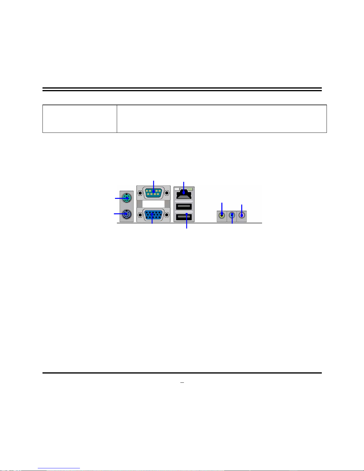
1-3 Layout Diagram & Jumper Setting
COM
Connector
RJ45 LAN
3
PS/2
Mouse
PS/2
Keyboard
MIC-IN
Line-Out
Line-In
VGA
Connector
USB
Connector
Page 9
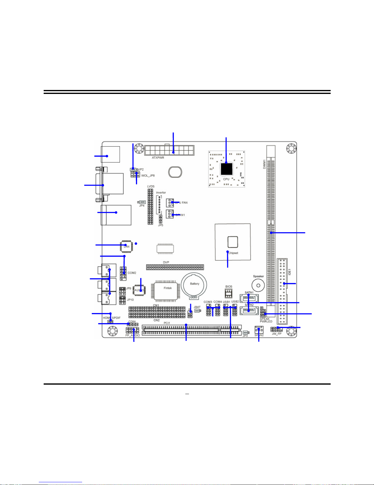
4
ATX Power Connector
C7/Eden/Nano
Keyboard/ USB Power (JP2)
PS2 KB/Mouse Port
VGA and COM
Connector
JP8
CPU FAN
USB Port Connector
SYS FAN1
DDRII Socket x1
COM Connector
RealtekRTL8111C
Gi
g
abit Lan
VIA 1708B
Audio Connector
VIA VX800
IDE Connecto
r
PCI Slot
SYS FAN2
Front Panel Connector
CD Audio-In
Header
SPDIF OUT
Front Panel Audio
Power LED
Speaker connecto
r
IR Connector
SATAII Connector (1,2)
COM Connector
USB Connector
Page 10

5
Jumper
Jumper Name Description Page
JP2
KB/USB Power On Function Setting 3-pin Block P.7
JBAT CMOS RAM Clear Function Setting 3-pin Block P.7
JP3 USB Power On Function Setting 3-pin Block P.8
JP4 LVDS5V/3.3V Select 3-pin Block P.8
JP8 Power RS232 Function Select 6-pin Block P.9
JP5 LVDS Inverter Power On Setting 3-pin Block P.9
JP9 Power RS232 Function Select 6-pin Block P.10
JP10 Power RS232/422/485 Function Select 6-pin Block P.10
Connectors
Connector Name Description Page
USB1,USB2 USB Port Connector 4-pin Connector P.11
UL2 RJ45 LAN Connector RJ-45 Connector
P.11
VGA Video Graphic Attach Connector D-sub15-pin Female
P.11
AUDIO1 Line-Out /MIC/Line-In Audio Connector 3 Phone Jack
P.11
COM1 Serial Port COM1 Connector 9-pin Connector
P.11
Page 11

6
Headers
Header Name Description Page
SYSFAN1, SYSFAN2 FAN Speed Headers 3-pin Block P.18
AUDIO2 Front panel audio Headers 9-pin block P.12
IR IR infrared module Headers 5-pin Block P.17
CDIN CD Audio-In Header 4-pin Block P.12
PWR LED Power LED 4-pin Block P.17
LVDS LVDS Connector 32-pin Block P.13
Inverter LVDS Inverter Connector 7-pin Block P.14
COM2,3,4 Serial Port COM1 Connector 9-pin Connector p.18
JW_FP
(PWR LED/ HD LED/ /Power
Button /Reset)
Front Panel Header
(PWR LED/ HD LED/ /Power Button
/Reset)
9-pin Block P.17
ATXPWR ATX Power Connector 24-pin Block p.10
SATA1~2
Serial ATAII IDE Connector 7-pin Connector p.11
Page 12
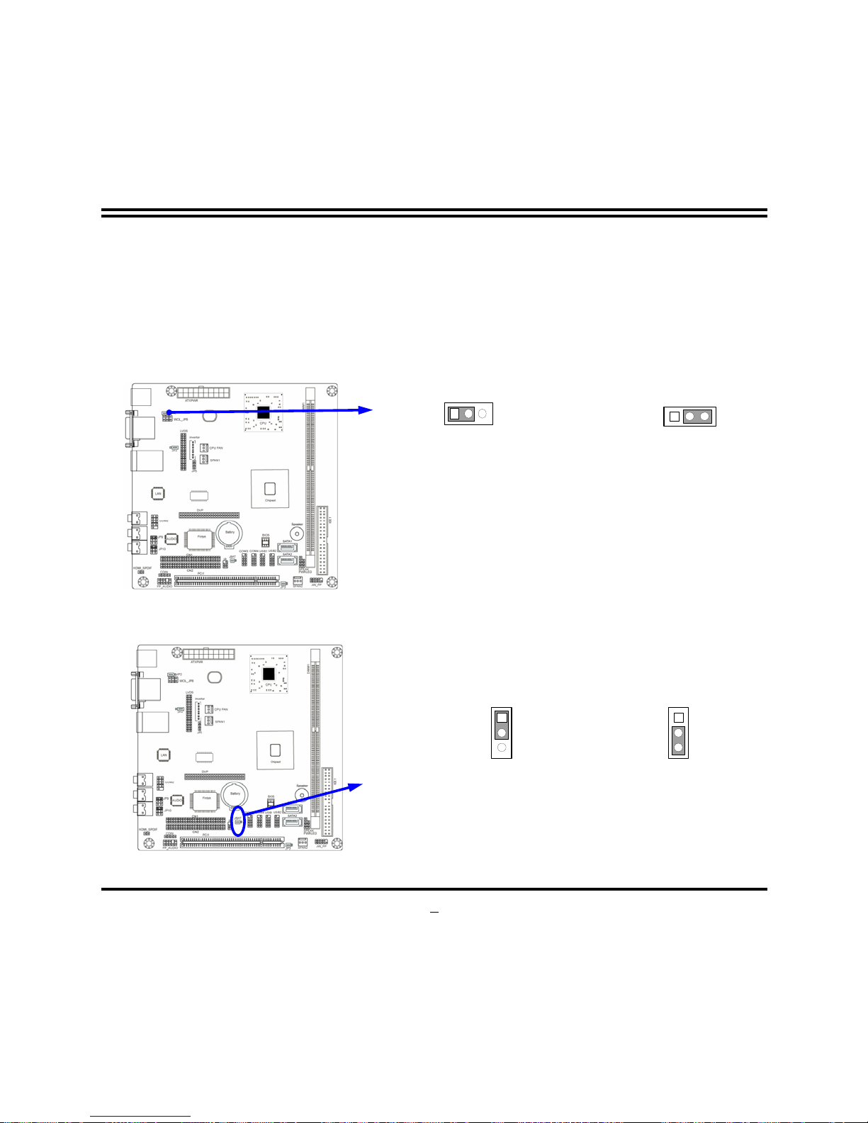
Chapter 2
2-1 Jumper Setting
(1) JP2: KB/USB Power On Function Setting
2-3 K.B& USB POWER-ON Enabled
JP2
JP2
1-2 K.B&USB POWER-ON Disacled
13
1 3
(2) Clear CMOS (3-pin): JBAT
CMOS RAM Clear Setting
2-3 closed Clear CMOS
JBAT
JBAT
1-2 closed Normal
1
3
1
3
7
Page 13

(3) JP3: USB Power On Function Setting (3-pin)
1-2 closed USB Power On Disabled
2-3 closed USB Power On Enabled
JP3
JP3
1
3
1
3
(4) JP4: LVDS 5V/3.3V Function setting (3-pin)
8
2-3 closed : PVDD= 3.3V
JP4
JP4
1
3
1-2 closed: PVDD=
1
3
5V
Page 14

(5) JP5: LVDS Inverter Function setting (3-pin)
9
(6) JP8: COM1 Pin 9 select
LVDS Function S etting
2-3 closed : LCD powered by 3.3V
JP5
JP8
1-2 closed: R
3-4 closed : +12V
1
S232
1
5-6 closed : +5V
1
1
3
JP5
1
3
1-2 closed: LCD Powered by 5V
Page 15

(7) JP9:COM2 Pin9 select
JP9
1-2 closed:
3-4 closed : +12V
1
RS232
11
5-6 closed : +5V
(8) JP10: RS232/422/485 Function Select
JP10
1-2 closed: R
10
3-4 closed : RS485
1
S232
1
5-6 closed : RS422
1
Page 16

2-2 Connectors and Headers
2-2-1 Connectors
(1) Audio Connector: (Line-IN/ Line-Out/ MIC-In)
11
(2) Serial-ATA Port connector: SATA1/SATA2
Serial-ATA Connectors
SATA2
SATA1
MIC-IN
RJ45 LAN
PS/2
Mouse
Line-Out
Line-In
USB
Connector
PS/2
Keyboard
VGA
Connector
COM
Connector
Page 17

2-2-2 Headers
(1) Front panel audio (9-pin): AUDIO2
12
Line-Out, MIC Headers
A
UDIO
Pin 1
MIC2-L
LINEOUT2-L
MIC2-R
LINEOUUT2-R
SENSE-FB
AUD
_
GND
Line2-JD
MIC2-JD
AUD
_
JD
2
9
10
(2) CD AUDIO-In Headers (4-pin): CDIN
CD Audio-In Headers
CDIN
GND
4 1
CD-R
CD-LGND
Page 18

13
(3) LVDS Headers: LVDS
Pin NO. Pin Define Pin NO. Pin Define
Pin 1
-LCD7
Pin 2
LCD7
Pin 3
-LCLK2
Pin 4
LCLK2
Pin 5
-LCD6
Pin 6
LCD6
Pin 7
-LCD5
Pin 8
LCD5
Pin 9
-LCD4
Pin 10
LCD4
Pin 11
GND
Pin 12
GND
Pin 13
GND
Pin 14
GND
Pin 15
GND
Pin 16
GND
Pin 17
LCD3
Pin 18
-LCD3
Pin 19
LCLK1
Pin 20
-LCLK1
Pin 21
LCD2
Pin 22
-LCD2
Pin 23
LCD1
Pin 24
-LCD1
Pin 25
LCD0
Pin 26
-LCD0
Pin 27
PVDD
Pin 28
PVDD
Pin 29
PVDD
Pin 30
PVDD
Pin 31
GND
Pin 32
GND
Page 19

14
Pin 1
LVDS Header
Pin 2
LVDS
(4) Pin-headers of LVDS Inverter:
Pin 1 and pin2: VCC of inverter
Pin3、pin4 and pin6: GND
Pin5: Backlight
Pin7: Brightness
VI
Pin 1
GN
Brightness
Backlight
GND
VI
GN
Page 20

(5) JWDB Header:
15
CN1
Pin NO. Pin Define Pin NO. Pin Define
Pin 1 GND Pin 2 GND
Pin 3 PCICLK2 Pin 4 -IRDY
Pin 5 -INTR_A Pin 6 +3.3V
Pin 7 -INTR_D Pin 8 -DEVSEL
Pin 9 -12V Pin 10 -PERR
Pin 11 LPC_24_48M Pin 12 -PERR
Pin 13 PCICLK3 Pin 14 +3.3v
Pin 15 PCICLK1 Pin 16 -SERR
Pin 17 GND Pin 18 +3.3v
Pin 19 -REQ1 Pin 20 C_-BE1
Pin 21 -REQ2 Pin 22 A_D14
Pin 23 A_D31 Pin 24 GND
Pin 25 A_D29 Pin 26 A_D12
Pin 27 GND Pin 28 A_D10
Pin 29 A_D27 Pin 30 GND
Pin 31 A_D25 Pin 32 A_D8
Page 21

16
Pin 33 +3.3V Pin 34 A_D7
Pin 35 C_-BE3 Pin 36 +3.3V
Pin 37 A_D23 Pin 38 A_D5
Pin 39 GND Pin 40 A_D3
Pin 41 A_D21 Pin 42 GND
Pin 43 A_D19 Pin 44 A_D1
Pin 45 LAD3 Pin 46 LAD0
Pin 47 A_D17 Pin 48 LAD1
Pin 49 C_-BE2 Pin 50 LAD2
CN2
Pin NO. Pin Define Pin NO. Pin Define
Pin 1 12V Pin 2 -FRAME
Pin 3 +5V Pin 4 GND
Pin 5 -INTR_C Pin 6 -TRDY
Pin 7 -REQ3 Pin 8 GND
Pin 9 -GNT3 Pin 10 -STOP
Pin 11 +3.3VSUS Pin 12 +3.3V
Pin 13 -PCIRSTX Pin 14 GND
Pin 15 -GNT2 Pin 16 PAR
Pin 17 -GNT1 Pin 18 A_D15
Pin 19 GND Pin 20 +3.3V
Pin 21 -PME Pin 22 A_D13
Pin 23 A_D30 Pin 24 A_D11
Pin 25 +3.3V Pin 26 GND
Pin 27 A_D28 Pin 28 A_D6
Pin 29 A_D26 Pin 30 C_-BE0
Page 22

Pin 31 GND Pin 32 +3.3V
Pin 33 A_D24 Pin 34 A_D6
Pin 35 A_D20 Pin 36 A_D4
Pin 37 +3.3V Pin 38 GND
Pin 39 A_D22 Pin 40 A_D2
Pin 41 +3.3VSUS Pin 42 A_D0
Pin 43 GND Pin 44 -LDRQ
Pin 45 A_D18 Pin 46 -LFRAME
Pin 47 A_D16 Pin 48 +5V
Pin 49 +3.3V Pin 50 GPIO1
(6) IR infrared module Headers (5-pin): IR
IR infrared module Header
IR
GND
+5VX
1
7
Pin 1
IRRX
GND
IRTX
2
6 5
Page 23

(7) JW-FP(9-pin)
System Case Connections
HDLED
RESET
VCC5
GND
VCC5
PWR LED
PWRBTN
18
(8) FAN Speed Headers (3-pin): CPUFAN, SFAN1/SFAN2
PWRBTN
PWRLED
GND
HDDLE
RSTSW
NC
JW FP
Pin 1
SPEAK
SPKR
GND
NC
VCC5
PWRLED
Pin 1
Pin 1
SYS FAN1
CPUFAN
SYS FAN2
Page 24

(9) COM Connectors (9-pin):
19
Pin No. Pin Definition Pin No. Pin Definition
Pin 1 DCD Pin 6 DSR
Pin 2 RXD Pin 7 RTS
Pin 3 TXD Pin 8 CTS
Pin 4 DTR Pin 9 RI
Pin 5 GND
Pin1
Serial COM Port 9-pin Block
Pin6
Page 25

20
Chapter 3
Introducing BIOS
Attention:
The BIOS options shown in this manual is for reference use only. We
reserve the right to update the BIOS version without advance notice.
The BIOS is a program located on a Flash Memory on the motherboard. This program is a
bridge between motherboard and operating system. When you start the computer, the BIOS
program will gain control. The BIOS first operates an auto-d ia gnostic test called POST (power
on self test) for all the necessary hardware, it detects the entire hardware device and
configures the parameters of the hardware synchronization. Only when these tasks are
completed done it gives up control of the computer to operating system (OS). Since the
BIOS is the only channel for hardware and software to communicate, it is the key factor for
system stability, and in ensuring that your system performance as its best.
In the BIOS Setup main menu of Figure 3-1, you can see several options. We will explain
these options step by step in the following pages of this chapter, but let us first see a short
description of the function keys you may use here:
• Press <Esc> to quit the BIOS Setup.
• Press ↑↓←→ (up, down, left, right) to choose, in the main menu, the option you want
to confirm or to modify.
• Press <F10> when you have completed the setup of BIOS parameters to save these
parameters and to exit the BIOS Setup menu.
• Press Page Up/Page Down or +/– keys when you want to modify the BIOS parameters
for the active option.
Page 26

21
3-1 Entering Setup
Power on the computer and by pressing <Del> immediately allows you to enter Setup.
If the message disappears before your respond and you still wish to enter Setup, restart the
system to try again by turning it OFF then ON or pressing the “RESET” button on the system
case. You may also restart by simultaneously pressing <Ctrl>, <Alt> and <Delete> keys. If
you do not press the keys at the correct time and the system does not boot, an error message
will be displayed and you will again be asked to
Press <F1> to continue, or <Del> to enter Setup
3-2 Getting Help
Main Menu
The on-line description of the highlighted setup function is displayed at the bottom of the
screen.
Status Page Setup Menu/Option Page Set up M enu
Press F1 to pop up a small help window that describes the appropriate keys to use and the
possible selections for the highlighted item. To exit the Help Window, press <Esc>.
3-3 The Main Menu
Once you enter Award® BIOS CMOS Setup Utility, the Main Menu (Figure 3-1) will appear
on the screen. The Main Menu allows you to select from fourteen setup functions and two
exit choices. Use arrow keys to select among the items and press <Enter> to accept or enter
the sub-menu.
Page 27

22
Phoenix – AwardBIOS CMOS Setup Utility
Standard CMOS Features
Advanced BIOS Features
Advanced Chipset Features
Integrated Peripherals
Power Management Setup
PnP/PCI Configurations
PC Health Status
Miscellaneous Control
Load Optimized Defaults
Load standard Defaults
Set Supervisor Password
Set User Password
Save & Exit Setup
Exit Without Saving
Esc : Quit F9 : Menu in BIOS
↑↓→←
: Select Item
F10 : Save & Exit Setup
Figure 3-1
Standard CMOS Features
Use this Menu for basic system configurations.
Advanced BIOS Features
Use this menu to set the Advanced Features available on your system.
Advanced Chipset Features
Use this menu to change the values in the chipset registers and optimize your system’s
performance.
Integrated Peripherals
Use this menu to specify your settings for integrated peripherals.
Power Management Setup
Page 28

23
Use this menu to specify your settings for power management.
Miscellaneous Control
Use this menu to specify your settings for
Miscellaneous Control
.
PC Health Status
This entry shows your PC health status.
Power User Overclock Settings
Use this menu to specify your settings (frequency, Voltage) for overclocking demand
CPU Thermal Throttling Setting
The selection is set for activating the active CPU Thermal Protection by flexible CPU loading
adjustment in the arrange of temperature you defined.
Load Optimized Defaults
Use this menu to load the BIOS default values these are setting for opt i m a l p e r f o r m a n c e s s y s t e m
operations for performance use.
Password Settings
This entry for setting Supervisor password and User password
Save & Exit Setup
Save CMOS value changes to CMOS and exit setup.
Exit Without Saving
Abandon all CMOS value changes and exit setup.
Page 29

24
3-4 Advanced BIOS Features
Phoenix – AwardBIOS CMOS Setup Utility
Advanced BIOS Features
Item Help
CPU Feature Press Enter
Hard Disk Boot Priority Press Enter
Virus Warning Disabled
CPU L1&L2 Cache Enabled
CPU L2 Cache ECC Checking Enabled
Quick power on self Test Enabled
First Boot Device HARD DISK
Second Boot Device CDROM
Third Boot Device LS120
Boot other Device Enabled
Boot Up NumLock Status On
Typematic Rate Setting Disabled
Typematic Rate (Chars/Sec) 6
Typematic Delay (Msec) 250
Security Option Setup
APIC Mode Enabled
MPS Version Control For OS 1.4
OS Select For DRAM > 64MB Non-OS2
HDD S.M.A.R.T. Capability Disabled
Video BIOS Shadow Enabled
Menu Level >
↑↓→←
Move Enter:Select +/-/PU/PD:Value F10:Save ESC:Exit F1:General Help
F5:Previous Values F6:Optimized Defaults F7:Standard Defaults
Hard Disk Boot Priority
The selection is for you to choose the hard disk drives priorities to boot from.
Virus Warning
The selection Allow you to choose the VIRUS Warning feature for IDE Hard Disk boot sector
protection. If this function is enabled and someone attempt to write data into this area, BIOS
will show a warning message on screen and alarm beep.
Page 30

25
Disabled
(default) No warning message to appear when anything attempts to access the
boot sector or hard disk partition table.
Enabled
Activates automatically when the system boots up causing a warning
message to appear when anything attempts to access the boot sector
of hard disk partition table.
CPU Internal Cache
The default value is Enabled.
Enabled
(default) Enable cache
Disabled
Disable cache
Note: The internal cache is built in the processor.
External Cache
Choose Enabled or Disabled. This option enables the Level 2 cache memory.
Quick Power On Self-Test
This category speeds up Power On Self Test (POST) after you power on the computer. If
this is set to Enabled, BIOS will shorten or skip some check items during POST.
Enabled
(default) Enable quick POST
Disabled
Normal POST
First/Second/Third Boot Device
The BIOS attempts to load the operating system from the devices in the sequence selected in
these items. The settings are Floppy, LS/ZIP, HDD-0/HDD-1/HDD-3, SCSI, CDROM,
LAD and Disabled.
Boot Up Floppy Seek
During POST, BIOS will determine if the floppy disk drive installed is 40 or 80 tracks.
360K type is 40 tracks while 760K; 1.2M and 1.44M are all 80 tracks.
Boot Up NumLock Status
The default value is on.
On
(default)
Keypad is numeric keys.
Off
Keypad is arrow keys.
Gate A20 Option
Normal
The A20 signal is controlled by keyboard controller or chipset hardware.
Fast
(default) The A20 signal is controlled by port 92 or chipset specific method.
Page 31

26
Typematic Rate Setting
Keystrokes repeat at a rate determined by the keyboard controller. When enabled, the
typematic rate and typematic delay can be selected. The settings are: Enabled/Disabled.
Typematic Rate (Chars/Sec)
Set the number of times a second to repeat a keystroke when you hold the key down. The
settings are: 6, 8, 10, 12, 15, 20, 24, and 30.
Typematic Delay (Msec)
Sets the delay time after the key is held down before beginning to repeat the keystroke. The
settings are 250, 500, 750, and 1000.
Security Option
This category allows you to limit access to the system and Setup, or just to Setup.
System
The system will not boot and access to Setup will be denied if the
correct password is not entered at the prompt.
Setup
(default) The system will boot, but access to Setup will be denied if the correct
password is not entered prompt.
HDD S.M.A.R.T Capability
This option allow you to enable the HDD S.M.A.R.T Capability (Self-Monitoring, Analysis
and Reporting Technology) . You can choose from Enabled and Disabled.
MPS Version Control For OS 1.4
This option is only valid for multiprocessor motherboards as it specifies the version of the
Multiprocessor Specification (MPS) that the motherboard will use.
OS Select For DRAM > 64MB
Allows OS2® to be used with >64MB or DRAM. Settings are Non-OS/2 (default) and OS2.
Set to OS/2 if using more than 64MB and running OS/2®.
Video BIOS shadow
Enabled copies video BIOS to shadow RAM Improves performance.
Page 32

2
7
3-4-1 CPU Feture
Phoenix – AwardBIOS CMOS Setup Utility
CPU Features
Item Help
Thermal Management Thermal Monitor 2
Thermal Monitor Bus Ratio 8x
Thermal Monitor Bus VID 0.700v
Menu Level >
↑↓→←
Move Enter:Select +/-/PU/PD:Value F10:Save ESC:Exit F1:General Help
F5:Previous Values F6:Optimized Defaults F7:Standard Defaults
Thermal Management
Thermal monitor 1 (on die throttling)
Thermal monitor 2 (Ratio&VID transition)
Thermal monitor 3 (Dynamic Ratio&VID transition)
Thermal Monitor Bus Ratio
Represent the frequency (bus ratio) of the throttled performance state that will be invited
when the on-diesensor goes from not hot to hot.
Thermal Monitor Bus VID
Represent the voltage of the throttled performance state that will be invited when the on
diesensor goes from not hot to hot.
Page 33

28
3-5 Intergrated peripherals
Phoenix – AwardBIOS CMOS Setup Utility
Intergrated peripheral
Item Help
Onboard IDE Function Press Enter
Onboard Device Function Press Enter
Onboard Superio Function Press Enter
USB Device Setting Press Enter
Init Display First PCI Slot
Menu Level >>
↑↓→←
Move Enter:Select +/-/PU/PD:Value F10:Save ESC:Exit F1:General Help
F5:Previous Values F6:Optimized Defaults F7:Standard Defaults
Phoenix – AwardBIOS CMOS Setup Utility
Onboard Device Function
Item Help
Onboard HD Audio Deivice Auto
Realtek Lan1 Device Enabled
Realtek Lan1 Bootrom Disabled
Menu Level >>
↑↓→←
Move Enter:Select +/-/PU/PD:Value F10:Save ESC:Exit F1:General Help
F5:Previous Values F6:Optimized Defaults F7:Standard Defaults
Onboard HD Audio
This item allows you to decide to enable/disable the chipset family to support HD Audio.
The settings are: Enabled, Disabled.
Onboard PCIE LAN Bootrom
Decide whether to invoke the boot ROM of the onboard LAN chip.
Page 34

29
3-6 PC Health Status
This section shows the Status of you CPU, Fan, and Warning for overall system status. This
is only available if there is Hardware Monitor onboard.
Phoenix – AwardBIOS CMOS Setup Utility
PC Health Status
Item Help
Shutdown Temperature Disabled
Show PC Health In Post Enabled
CPU Thermal-Throttling Disabled
CPU Thermal-Throttling Temp 70c
CPU Thermal-Throttling Duty 50%
CPU Thermal-Throttling Beep Enabled
Smart fan configurations Press Enter
Vcore 0.97V
+1.5v 1.49V
+5v 5.02v
+12v 11.98v
+5VSB 5.06V
VDIMM 1.84V
VCC3 3.42V
3.3 SUS 3.34V
VBAT 3.22V
CPU Temperature 54c/129F
SYS Temperature 33c/93F
CPU FAN Speed 0RPM
SYS FAN1 Speed 0RPM
SYS FAN2 Speed 0RPM
Menu Level >
↑↓→←
Move Enter:Select +/-/PU/PD:Value F10:Save ESC:Exit F1:General Help
F5:Previous Values F6:Optimized Defaults F7:Standard Defaults
Show PC Health in Post
During Enabled, it displays information list below. The choice is either Enabled or Disabled
CPU Smart FAN Configurations
CPU Full-Speed Temp
This item allows you setting the FAN works in full speed when the temperature over the value
Page 35

30
which out set. If the temperature below the value but over the Idle Temperature, the FAN
will works over 60% of full speed, and the higher temperature will gain higher FAN speed,
after over the temperature which this item setting, the FAN works in full speed.
CPU Idle Temp
This item allows you setting the FAN works in 60% of full speed, when the temperature
lower than the temperature which you setting.
Current CPU Temperature/Current System Temp/Current FAN1, FAN2 Speed/Vcore/
Vdd/3.3V/+5V/+12V/-12V/VBAT(V)/5VSB(V)
This will show the CPU/FAN/System voltage chart and FAN Speed.
3-7 Advanced Chipset Features
The Advanced Chipset Features Setup option is used to change the values of the chipset
registers. These registers control most of the system options in the computer.
Phoenix – AwardBIOS CMOS Setup Utility
Advanced Chipset Features
Item Help
DRAM Timing Settings Press Enter
VGA Timing Settings Press Enter
PCI Timing Settings Press Enter
Memory Hole Disabled
System BIOS Cacheable Enabled
VIDEO RAM Cacheable Disabled
Menu Level >
↑↓→←
Move Enter: Select +/-/PU/PD: Value F10:Save ESC: Exit F1:General Help
F5:Previous Values F6:Optimized Defaults F7:Standard Defaults
System BIOS Cacheable
Selecting Enabled allows caching of the system BIOS ROM at F0000h-FFFFFh, resulting in
better system performance. However, if any program writes to this memory area, a system
error may result. The settings are: Enabled and Disabled.
Page 36

31
3-8 Power Management Setup
The Power Management Setup allows you to configure your system to most effectively save
energy saving while operating in a manner consistent with your own style of computer use.
Phoenix – AwardBIOS CMOS Setup Utility
Power Management Setup
Item Help
ACPI Suspend Type S1(POS)
Assign IRQ For ACPI IRQ 9
Video off option Suspend-off
SYC+Blank Video off Method V/H
MODEN USE IRQ 3
Power Button Function Instant off
FF Power after power Function Always O
HPET Support Enabled
led WDRT Support Disab
WDRT Run/stop Stop
WDRT Count 1023
Wake UP Events Press Enter
Menu Level >
↑↓→←
elp Move Enter:Select +/-/PU/PD:Value F10:Save ESC:Exit F1:General H
F5:Previous Values F6:Optimized Defaults F7:Standard Defaults
ACPI Function
This item allows you to Enabled/Disabled the Advanced Configuration and Power
Management (ACPI). The settings are Enabled and Disabled.
Video Off Method
This determines the manner in which the monitor is blanked.
DPMS (default)
Initial display power management signaling.
Blank Screen
This option only writes blanks to the video buffer.
V/H SYNC+Blank
This selection will cause the system to turn off the vertical and
horizontal synchronization ports and write blanks to the video buffer.
MODEM Use IRQ
If you want an incoming call on a modem to automatically resume the system from a
power-saving mode, use this item to specify the interrupt request line (IRQ) that is used by
Page 37

32
the modem. You might have to connect the fax/modem to the motherboard Wake On Modem
connector for this feature to work.
Soft-Off by PWRBTN
Under ACPI (Advanced Configuration and Power management Interface) you can create a
software power down. In a software power down, the system can be resumed by Wake up
Alarms. This item lets you install a software power down that is controlled by the power
Button on your system. If the item is set to Instant-Off, then the power button causes a
software power down. If the item is set to Delay 4 Sec, then you have to hold the power
button down for four seconds to cause a software power down.
3-9 PnP/PCI Configuration
Phoenix – AwardBIOS CMOS Setup Utility
Pnp/PCI Configuration
Item Help
IRQ Resources Press Enter
PCI/VGA Palette Snoop Disabled
Assign IRQ For VGA Enabled
Assign IRQ For USB Enabled
Menu Level >
↑↓→←
Move Enter:Select +/-/PU/PD:Value F10:Save ESC:Exit F1:General Help
F5:Previous Values F6:Optimized Defaults F7:Standard Defaults
Page 38

33
3-10 Miscellaneous Configuration
Phoenix – AwardBIOS CMOS Setup Utility
Miscellaneous Control
Item Help
Spread Spectrum Disabled
Current Host Frequency is 200MHz
CPU Clock at Next boot is 200MHz
Current DRAM Frequency is 333MHz
DRAM Clock at Next Boot is SPD
CPU Clock Ratio is 8x
Vcore voltage Default
VCC1.05 Voltage Auto
VCC 1.5 Voltage 1.50v(Default)
VDIMM Voltage 1.84v(Default)
Menu Level >
↑↓→←
Move Enter:Select +/-/PU/PD:Value F10:Save ESC:Exit F1:General Help
F5:Previous Values F6:Optimized Defaults F7:Standard Defaults
Page 39

34
Phoenix – AwardBIOS CMOS Setup Utility
Miscellaneous Control
Item Help
Auto Detect PCI CLK Enabled
Spread Spectrum Disabled
Current Host Frequency is 100MHz
CPU Clock at Next boot is 100MHz
Current DRAM Frequency is 333MHz
DRAM Clock at Next Boot is SPD
CPU Clock Ratio is 8x
Vcore voltage Default
VCC1.05 Voltage 1.05v(Default)
VCC 1.5 Voltage 1.50v(Default)
VDIMM Voltage 1.84v(Default)
Menu Level >
V
CC 1.5 Voltage
1.00v [ ]
1.02v [ ]
1.05v [ ]
………
1.25v [ ]
↑↓:Move ENTER:Accept
ESC:Abort
↑↓→←
Move Enter:Select +/-/PU/PD:Value F10:Save ESC:Exit F1:General Help
F5:Previous Values F6:Optimized Defaults F7:Standard Defaults
Page 40

35
Phoenix – AwardBIOS CMOS Setup Utility
Miscellaneous Control
Item Help
Auto Detect PCI CLK Enabled
Spread Spectrum Disabled
Current Host Frequency is 100MHz
CPU Clock at Next boot is 100MHz
Current DRAM Frequency is 333MHz
DRAM Clock at Next Boot is SPD
CPU Clock Ratio is 8x
Vcore voltage Default
VCC1.05 Voltage 1.05v(Default)
VCC 1.5 Voltage 1.50v(Default)
VDIMM Voltage 1.84v(Default)
Menu Level >
V
core Voltage
-7.5% [ ]
-5.0% [ ]
-2.5% [ ]
Default
………
+2.5% [ ]
+30.5% [ ]
↑↓:Move ENTER:Accept
ESC:Abort
↑↓→←
Move Enter:Select +/-/PU/PD:Value F10:Save ESC:Exit F1:General Help
F5:Previous Values F6:Optimized Defaults F7:Standard Defaults
CPU Vcore
This item allows you select the CPU Vcore Voltage xx% more than the standard value, by
this function for the precise over-clocking for extra demanding of performance.
VDIMM Voltage
This item allows you select the voltage of the memory.
 Loading...