

Page 1

694X PRO
(VIA VT82C694X、4 x AGP、PC-133)
ATX Form Factor
Main Board
User's Manual
(Ver.:1.0)
Page 2

Copyright
Copyright© 2001 by this company. No part of this document may be
reproduced, transmitted, transcribed, stored in a retrieval system, or
translated into any language or computer language, in any form or
by any means without prior written permission. This manual and the
information contained herein are protected by copyright. All rights
reserved.
Manual version: 1.0
Ref. No. 3053321
Published in 2001
Page 3

Warning and Disclaimer
This manual is designed to provide information about the Pentium®
II/III system board. Every effort has been made to make this manual
as accurate as possible, but no warranty or fitness is implied. All the
information is provided on an 'as is' basis. The author and his
corresponding publishing company shall have neither liability nor
responsibility to any person or entity with respect to any loss or
damages arising from the information contained in this manual or
from the use of the system board that accompanies it.
Information contained in this manual is subject to change without
notice. The manufacturer of the main board will not be held
responsible for technical or editorial omissions made herein, nor for
the incidental or consequential damages resulting from its
furnishing, performance, functionality or use. Subsequent changes to
this manual will be incorporated into the next edition. We welcome
any suggestion regarding this manual or our computer products.
Trademarks
● Intel
®
and Pentium® are registered trademarks of Intel®
Corporation.
● IBM
®
is a registered trademark of International Business
Machines Corporation.
● Microsoft
®
is a registered trademark of Microsoft® Corporation.
● PCI
®
is a registered trademark of PCI Special Interest Groups.
● AWARD
®
is a registered trademark of Award Software Inc.
All other trademarks are the property of their respective owners.
Page 4

694X PRO System Board I
Table of Contents
Chapter 1 Introduction………………………………………..….…………1
1-1 Main Board Overview…………………………………………………1
1-2 Specifications.……………………………………………………..……3
1-3 Notice of Hardware Installation…………………..……………....……6
1-4 Notice of CD Driver Installation…………………..…………………7
Chapter 2 Installation………………………….……………………….…8
2-1 Layout Reference…………………………..…………………..………..8
2-2 Jumper Setting.…………………...…………………….…………….…9
2-2-1 RTC1 : CMOS Status…….……………….……...…………………….9
2-2-2 JP1 : CPU Type Selector…………………………….…………………10
2-2-3 VID0-VID4 : CPU Vcore Selector………………………………….11
2-2-4 JP4-JP7 : AMR Function Selector…..………………………………13
2-2-5 JP8,JP3 : Over-clocking Setup……………………………………….14
2-3 Connectors ………………………………..……………………………15
2-3-1 Front Panel…………………………………………………….………15
2-3-2 Back Panel…………………………………………….……………….17
Keyboard &Mouse..…… ………………………………………………18
USB1/USB2(Universal Serial Bus)……………………………………..18
COM1/COM2………………………………………………………..…18
LPT1 (Parallel Port)……………………………………………………18
2-3-3 ATX Power Supply Connector…...…………………….…………….19
2-3-4 CPU Fan Connectors………………….……………..……………..…20
2-3-5 I.R. : IrDA Connector………………………...……..………………21
2-3-6 Floppy Disk Connector……………………..……..……....………...22
2-3-7 IDE1 & IDE2..………………….…......………………..………...……23
2-4 DIMM Memory Installation…….…………………….….…………24
Page 5

694X PRO System Board II
Chapter 3 PhoenixNetTM BIOS Porting Guide……………………………26
3-1 Product Overview………………………………………………………26
3-2 Graphical Launch
Screen(GLS)……………………………………….27
Chapter 4 BIOS Setup..……...….…….. …………………………………28
4-1 Award BIOS CMOS Setup…………………………………………28
4-1-1 Standard CMOS Setup………………………………………………29
4-1-2 Advanced BIOS Features……………………………………………32
4-1-3 Advanced Chipset Features……………………………………..……37
4-1-4 Integrated Peripherals……………………………………..……...41
4-1-5 Power Management Setup……………………………………….46
4-1-6 PNP/PCI Configuration Setup……………………………………….52
4-1-7 PC Health Status…………...…………………………. ……………54
4-1-8 Frequency/Voltage Control.…………………………………………55
4-1-9 Load Optimized Defaults……………………………………………56
4-1-10 Supervisor/User Password……………………………………………57
4-1-11 Save and Exit Setup……..……………………………….……………60
4-1-12 Quit Without Saving…………………………………………………..61
Chapter 5 Appendix……………………………………………………….62
5-1 Memory Map…………………………………………….……………62
5-2 I/O Map……………………………………………………….………63
5-3 Time & DMA Channels Map…………………………………………64
5-4 Interrupt Map…………………………………………...….………….65
5-5 RTC & CMOS RAM Map…………………………………………66
5-6 Award BIOS Hard Disk Type………………………………………...67
5-7 ISA I/O Address Map………………………………….……………....69
Chapter 6 Q & A……………………………………………………………71
6-1 Error Messages During Power On Self Test………………………....71
Page 6

694X PRO System Board III
Page 7

VIA694X System Board 1
Chapter 1 Introduction
1-1 Main Board Overview
The main board is a new-generation INTEL Celeron/FC-PGA Pentium
®
III;Cyrix
MIII main board designed based on VIA VT82C694X chipset. The main board
has integrated the latest advances in processor, memory, I/O technologies into an
ATX form factor.
The main board utilizes VIA 694X chipset designed for INTEL Celeron/FC-PGA
Pentium
®
III;Cyrix MIII CPUs and supports new architects such as high-speed
2X/4X mode AGP graphic port, SDRAM, Ultra DMA/66, bus master IDE and
USB port. It has three Dual In-line Memory Modules (DIMM) which can be
installed with SDRAM memory. The memory subsystem supports up to either 384
MB (SDRAM). The main board using the Socket370, accepts Intel
®
Pentium®
II/III(100/133 MHz) processors. Built-in second level (L2) cache in CPU, there is
no cache necessary in this system board.
The main board also has implemented VIA VT82C686A high performance I/O
Controller utilizes with fully Plug and Play device which supports 2.88 MB
Floppy, Dual 16550 Compatible (with 16 bytes FIFO, up to 460K baud rate)
Serial Port, ECP (Enhanced Capabilities Port), EPP (Enhanced Parallel Port)
parallel port, Infrared IrDA (HPSIR), Amplitude Shift Keyed IR. (ASKIR) port
and Audio.
The main board supports 5*PCI, 1*A.G.P and 1*AMR. (four PCI Bus Mastering
slots & 1 PCI Bus Slave slot) for highest performance I/O add-on adapter cards.
Page 8

VIA694X System Board 2
The main board is also strengthened with Power Management Wake up Event
such as “WOL (Wake up on LAN),” “Modem ring on” which are the new
inventions to enable PCs to be turned on over the network. These are also key
benefits in PC operation, asset management, new system setup and power
conservation.
In conclusion, the main board is a combination of the highest in performance,
flexibility, efficiency, and ease of use that meets a variety of price/performance
levels. The main board is an ideal platform for the increasing requirements of
today’s and future’s desktop application.
This main board supports to 4X mode AGP card specially.
Page 9

VIA694X System Board 3
1-2 Specifications
● PCB board size : 30.5 cm x 19.00 cm
● PCB layer : 4 layers
● Socket 370
Support Intel® Celeron CPU at 66/100 MHz F.S.B and FC-PGA Pentium III
CPU at 100 MHz/133 MHz F.S.B. , Cyrix III CPU
CPU is not enclosed in the package.
● Memory DIMM : 3 of 168-pin 3.3V DIMM
● Expansion Slot :, 5 x PCI slots, 1x A.G.P. slot and 1 x AMR( allows primary
card only)
Supports 1X/2X/4X AGP mode.
● Chipset
• VIA VT82C694X
• VIA VT82C686A
● BIOS: flash ROM for BIOS
Award® full PnP (Plug & Play) BIOS
● I/O function
• 2 x PCI IDE devices
• 1 x FDC, 2 x serial ports(16550 fast com)
• 1 x parallel port device /EPP/ECP/SPP
• 2 x USB connector (4 port, 2 port optional)
• IrDA (infrared) connector
Page 10

VIA694X System Board 4
● Green function : Complied with APM (Advanced Power Management)
● ATX form factor
The ATX form factor has been defined to address four major areas of
improvement required of today’s predominant form factors.
• Enhance PC ease-of-use with all built-in I/O connector
• Better support for current and future I/O
• Reduce total system cost
• Better support for future processor technology
ATX is an evolution of the popular Baby-AT form factor. By mounting the
power supply on its side, the processor is relocated away from the expansion
slots, and the longer side of the board is used to host more on-board I/O
connector; this placing of I/O on the board reduces cabling inside the box,
lower costs, and improves reliability and ease-of use. A flexible I/O panel
allows ATX to support all current and future I/O requirements. The ATX
power supply will directly suck the air out of chassis that will save the cost of
a secondary fan in the system. System cost is further reduced by the higher
integration of PC components onto the system board itself, saving materials,
inventory holding, and assembly cost.
● Power supply regulation
Onboard switching voltage that supports appropriate power to the CPU and
future upgraded CPUs.
Page 11
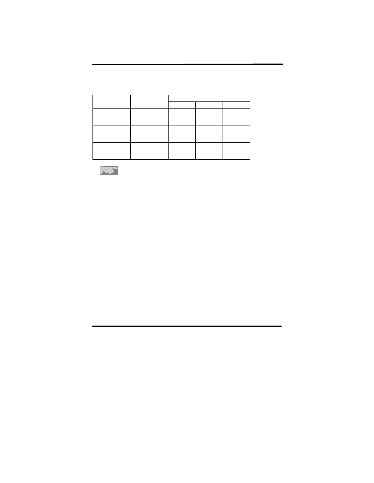
VIA694X System Board 5
● Electrical--- Typical power supply
Below is reference for ATX case requirement on power supply.
Current
Voltage Tolerance
230W 250W 300W
+5V
± 5%
23A 25A 30A
+3.3V
± 5%
14A 14A 14A
+12V
±10%
9A 10A 12A
-5V
± 5%
0.5A 0.5A 0.5A
-12V
± 5%
0.8A 0.8A 0.8A
+5VSB
± 5%
1A 1A 1A
WOL (Wake up on LAN) function requirement:
Power supply should offer at lest 1A to the signal “5VSB”to support WOL function.
● Special features
• Wake up on LAN (ATX power supply is required)
• Modem ring on
• Windows 95/98/2000 power off (ATX power supply is required)
• AMR
Page 12

VIA694X System Board 6
1-3 Notice of Hardware Installation
Before hardware installation, make sure you have checked the following
things.
A. Check the package
If any of these items is missing or damaged, contact the dealer from whom
you purchase. Leave this main board in its original package until you are
ready to install it. In the package, there are:
• the main board
• manual
• cables
• driver & utility / CD
B. Make sure power is off.
During hardware installation, be sure that there is no power connected at this
period.
C. Avoid ESD (Electrical Static Discharge)
While working with the main board, wear a grounded wristband or ankle strap
to avoid ESD (Electrical Static Discharge).
Page 13
VIA694X System Board 7
1-4 Notice of CD Driver Installation
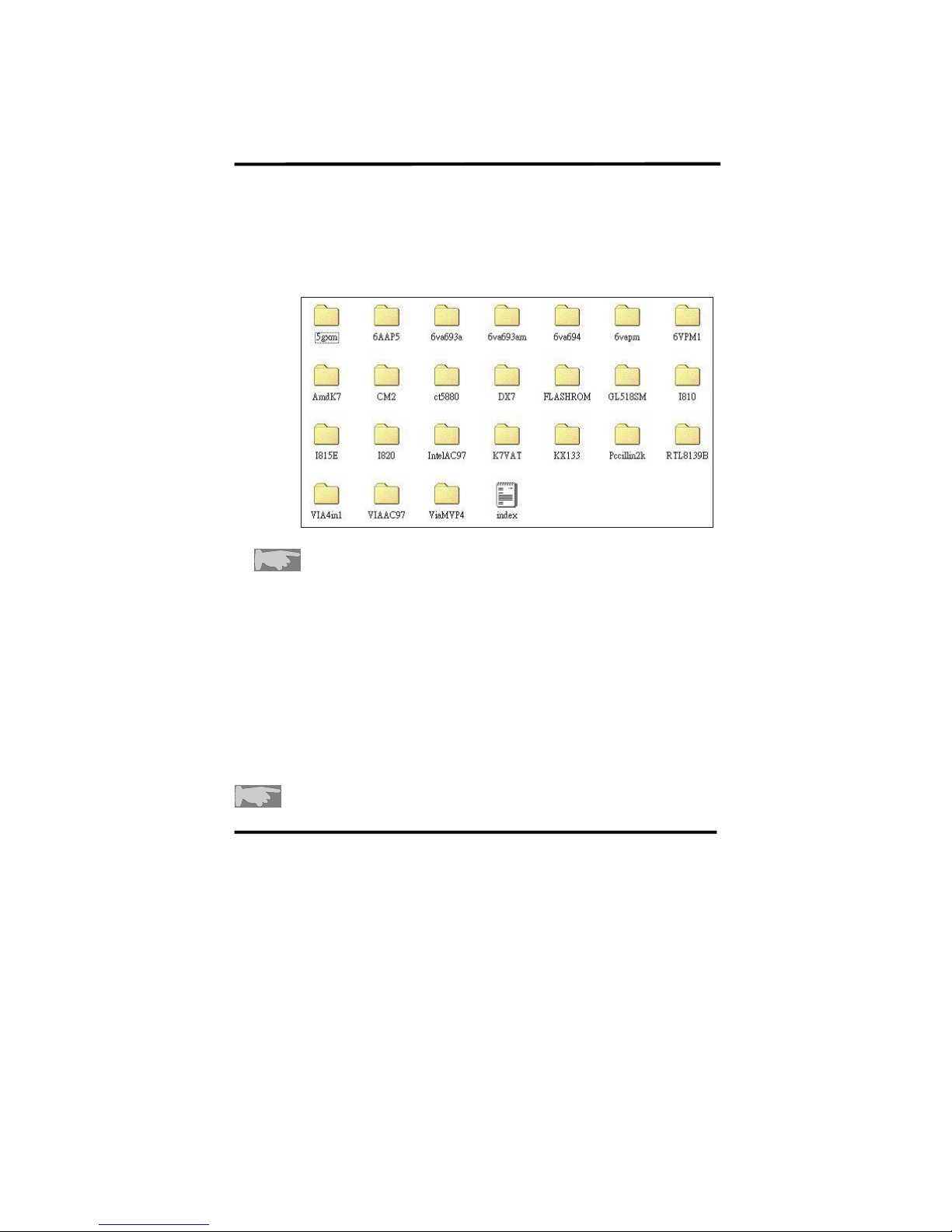
This CD contains drivers as below. Read “Index” before installing required
drivers. “Index” file is HTML format.
CD driver is always updated with the latest version, so the actual
CD content may have some differences with the above picture.
1. Main boards: 5gxm, 6AAP5, 6va693a, 6va693am, 6va694, 6vapm, 6VPM1,
Amdk7, I810, I815e, I820, K7vat, Kx133, ViaMVP4 (please choose 6va694
directory for this main board).
2. DX7:Windows DirectX7 driver.
3. Flashrom:Bios flashupgrade utility.
4. Pccillin2K: anti- virus protection software.View the on-line help for more
information.
5. VIA 4 in 1:Intall VIA 4 in 1 drivers V4.24 that automatically detect and
install the Bus Master PCI IDE driver. VIA AGP Driver, VIA INF Driver &
IRQ Routing Driver.
Due to “CIH” virus will damage BIOS completely, user needs to load
Pc-cillin anti-virus software when sets up system.
Page 14
VIA694X System Board 8
Chapter 2 Installation
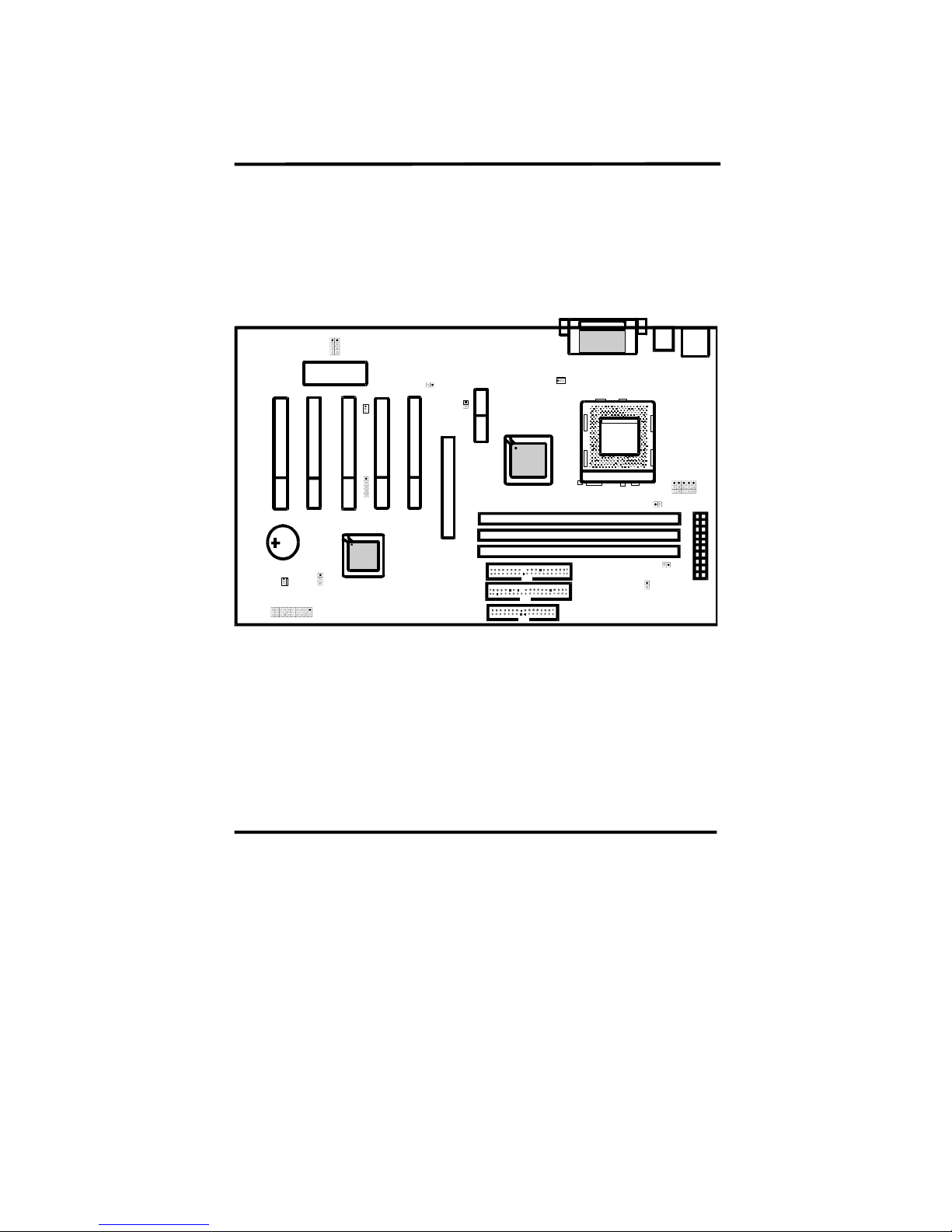
2-1 Layout Reference
COM2
COM1
LPT
USB1
K/B &
MOUSE
PGA370
FAN1
DIMM3
DIMM2
DIMM1
JP3
JP8
IDE2
IDE1
FDD1
VT82C694X
BIOS
AMR
AGP1
PCI1
PCI2PCI3PCI4PCI5
JP4
JP7
VID0
VID3
VID1
VID2
VID4
VT82C686A
RTC1
FAN2
J1
USB2
WOL1
TR1
JP1
ATX P ow er
Page 15
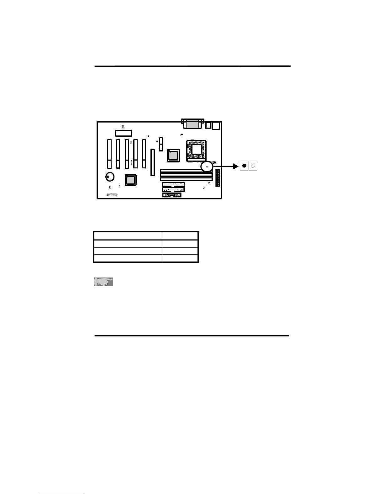
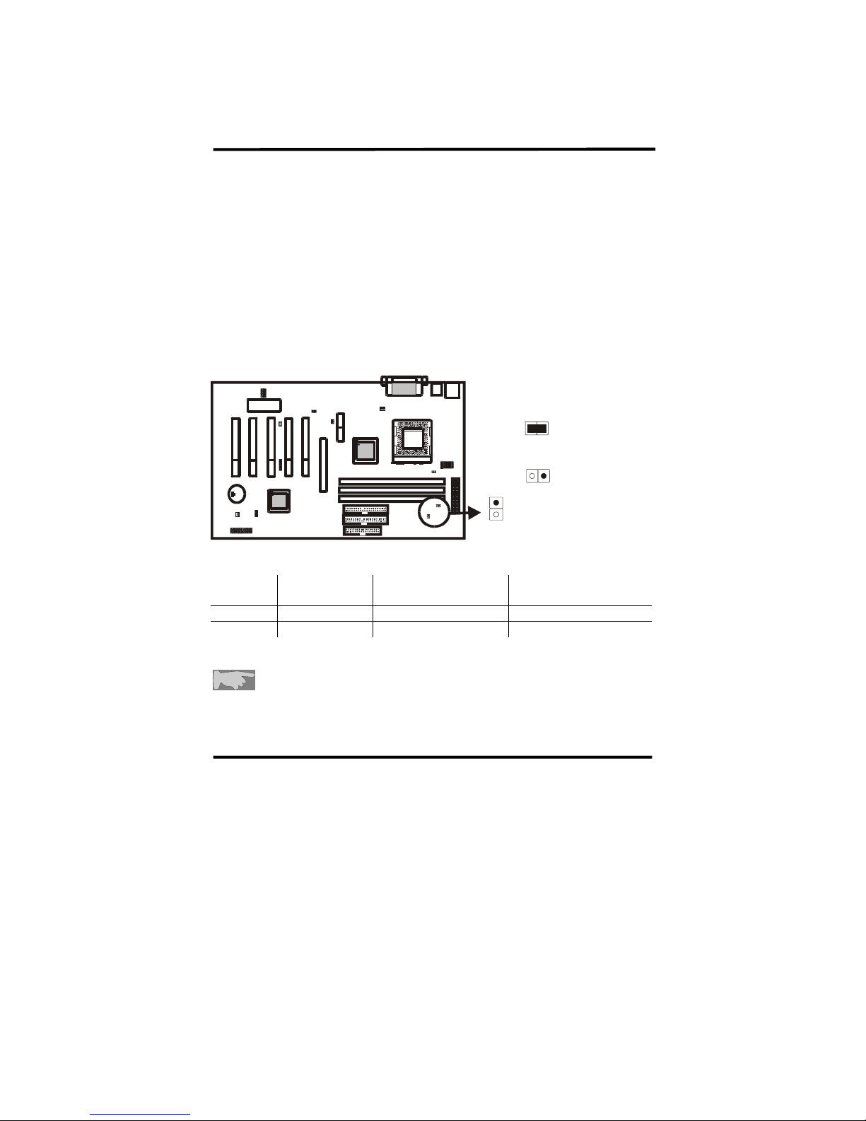
VIA694X System Board 9
2-2 Jumper Setting
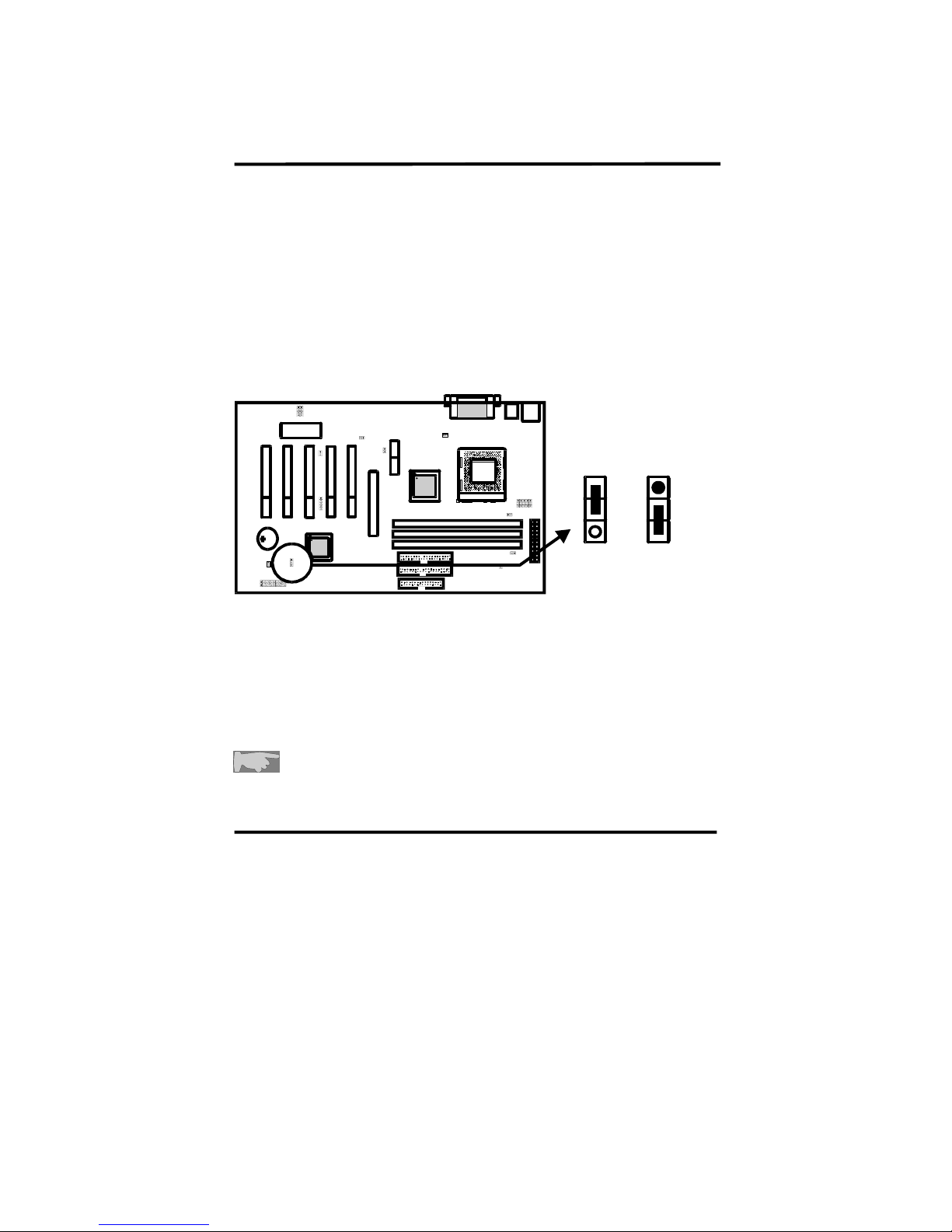
2-2-1 RTC1 - CMOS Status
RTC1 is a 3-pin connector. Clear CMOS if system password is forgotten. Below
are details to show how to clear CMOS.
RTC1:CMOS Status
Set to "1-2"---Set to "2-3"--Normal Clear CMOS
Procedure to clear CMOS:
Step 1: Shut down the system and disconnect the power supply from AC power.
Step 2: Pull out the ATX cable from ATX connector “POWER1”.
Step 3: Short the CMOS jumper by putting jumper cap on Pin 2-3 for a few seconds.
Step 4: Return to pin 1-2 for normal setup.
Step 5: Link ATX power cable to ATX connector & connect AC power to power supply.
Step 6: Turn on system power.
If you’d like to set password, press “DEL” Key during system bootup to enter
CMOS setup and establish a new password.
Page 16
VIA694X System Board 10
2-2-2 JP1 : CPU Type Selector
JP1 is 2-pin connector, which provides to select CPU type.
JP1:CPU Type Selector
CPU Type JP1
INTEL FC-PGA PIII CPU CLOSE
Cyrix III CPU OPEN
INTEL PII Celeron CPU OPEN
Remarks : JP1 : FC-PGA Coppermine/Celeron/Cyrix selector.
Page 17
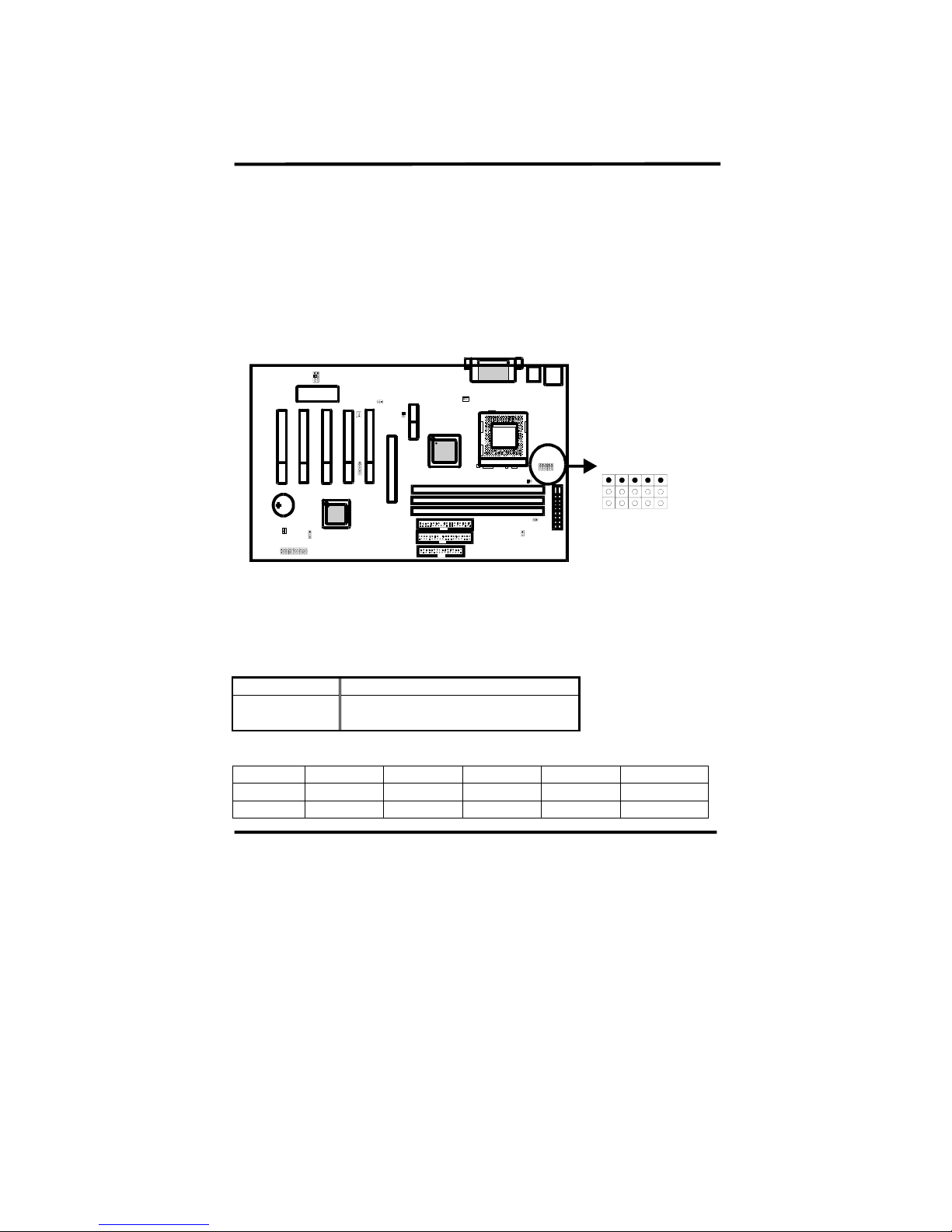
VIA694X System Board 11
2-2-3 VID0-VID4 : CPU Vcore Selector
VID0-VID4 are 3-pin connectors which provides CPU Vcore selection. Please
select the right Vcore according to your CPU and set details as below.
VID0-VID4 :CPU
Vcore Selector
VID0
VID1
VID2
VID3
VID4
VID0-VID3 VID4
Default(1-2) Default(2-3) : for Socket370 Intel
PII/PIII CPU, Cyrix III CPU
VID0 VID1 VID2 VID3 VID4 CPU_Volt.
2-3 1-2 1-2 2-3 1-2
2.9V
1-2 1-2 1-2 2-3 1-2
2.8V
Page 18
VIA694X System Board 12
2-3 2-3 2-3 1-2 1-2
2.7V
1-2 2-3 2-3 1-2 1-2
2.6V
2-3 1-2 2-3 1-2 1-2
2.5V
1-2 1-2 2-3 1-2 1-2
2.4V
2-3 2-3 1-2 1-2 1-2
2.3V
1-2 2-3 1-2 1-2 1-2
2.2V
2-3 1-2 1-2 1-2 1-2
2.1V
1-2 1-2 1-2 1-2 1-2
2.0V
2-3 2-3 2-3 2-3 2-3
2.05V
1-2 2-3 2-3 2-3 2-3
2.00V
2-3 1-2 2-3 2-3 2-3
1.95V
1-2 1-2 2-3 2-3 2-3
1.90V
2-3 2-3 1-2 2-3 2-3
1.85V
1-2 2-3 1-2 2-3 2-3
1.80V
2-3 1-2 1-2 2-3 2-3
1.75V
1-2 1-2 1-2 2-3 2-3
1.70V
2-3 2-3 2-3 1-2 2-3
1.65V
1-2 2-3 2-3 1-2 2-3
1.60V
2-3 1-2 2-3 1-2 2-3
1.55V
1-2 1-2 2-3 1-2 2-3
1.50V
2-3 2-3 1-2 1-2 2-3
1.45V
1-2 2-3 1-2 1-2 2-3
1.40V
2-3 1-2 1-2 1-2 2-3
1.35V
1-2 1-2 1-2 1-2 2-3
1.30V
Please don’t change default setting. The manufacturer shall have neither
liability nor responsibility to any person or entity with respect to any loss or
damages arising by users’ over-clocking or over-voltage.
Page 19
VIA694X System Board 13
2-2-4 JP4-JP7 : AMR Function Selector(Optional)
JP4-JP7 are 2-pin connectors which provide AMR function. Please see details as
below.
JP7
OFF
Primary CODEC for AMR(default)
JP4
ON
Use AMR Slot(default)
Only Support Primary Card For AMR Slot
JP4,JP7:AMR
Function Selector
JP4
JP7
Page 20
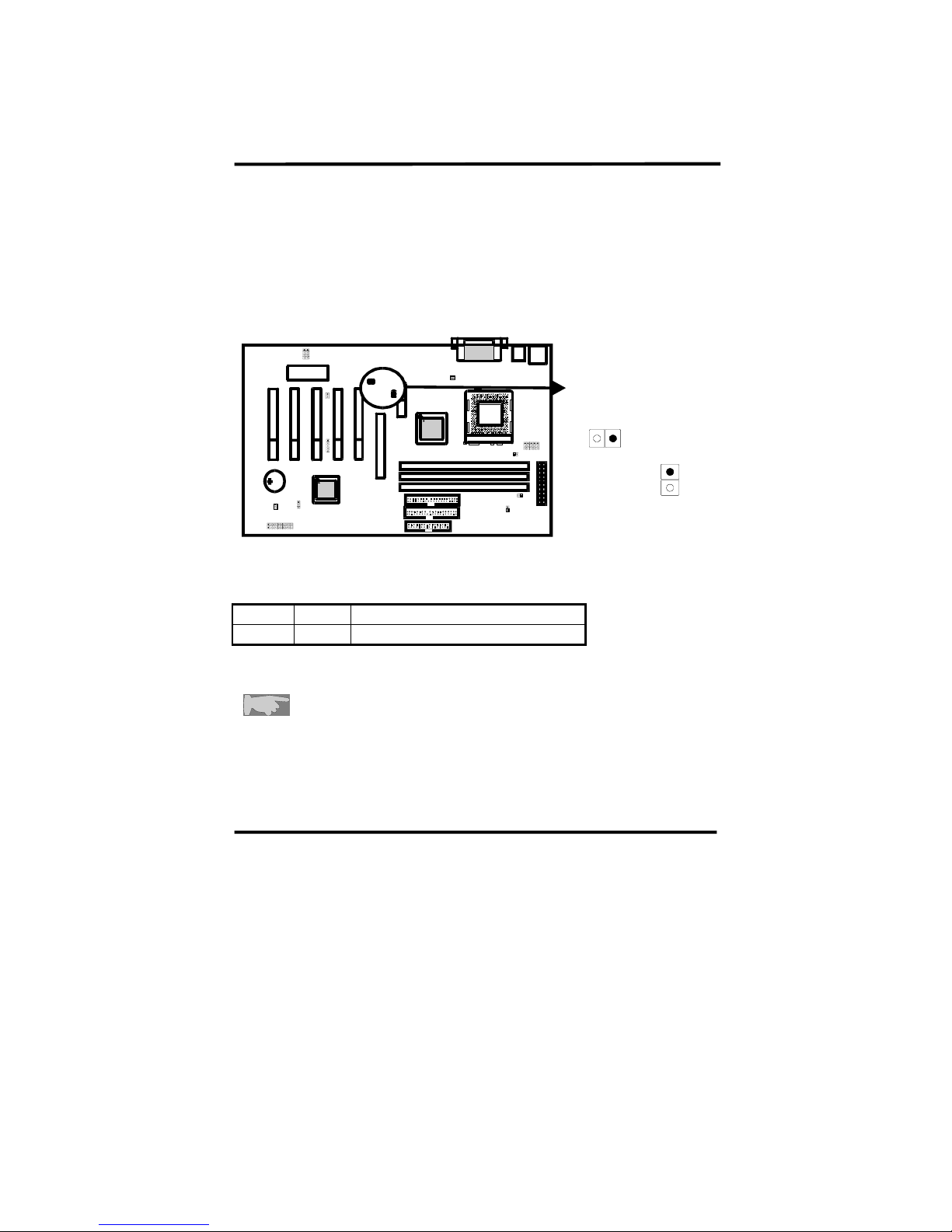
VIA694X System Board 14
2-2-5 JP8、JP3:Over-clocking Setup
JP8 is a 2-pin over-clocking jumper which allows 66MHz F.S.B. CPUs to
over-clock to 100MHz. This jumper is for internal test only. No guarantee is
provided for over-clocking setup since the chipset does not support.
JP3
:
is a 2-pin over- clocking jumper which allows 100MHz F.S.B. CPUs to
over-clock to 133MHz
Normal
Over-clocking 66MHz
to 100MHz
Over-clocking 100MHz
to 133MHz
JP8 ON OFF ON
JP3 ON ON OFF
The manufacturer shall have neither liability nor responsibility to any person
or entity with respect to any loss or damages arising by users’ over-clocking or
over-voltage.
JP3,JP8:Over-clocking Setup
Normal
Over-clocking
JP3
JP8
Page 21
VIA694X System Board 15
2-3 Connectors
There are many connectors on this main board. Refer to the following pages for
details.
2-3-1 Front Panel
Front panel has connectors as ““RESET,” “EXTSMI,” “HD-LED,” “PW-BT,”
“SPEAKER,” and “PW-LED”. Please refer to details as below.
RESET
EXTSMI HD-LED
PW-BT
SPEAKER
PWR LED
Page 22

VIA694X System Board 16
EXTSMI connector is a 2-pin Berg strip which is also called “green” or “sleep”
connector. When EXTSMI is turned from open to close and back to open, the
system will enter sleep mode immediately. This function is to make sure power
saving is working well. In PC system, it is used to connect to the push button
EXTSMI switch located on the case front panel (if there is). The system can be
forced to power saving mode by pressing the EXTSMI switch.
PW-BT with a 2-pin Berg strip on case front panel indicates the current power
status of system. It is used to connect to the Power Button on the front panel of the
case (if there is).
Marked as “HD-LED,” Hard Disk activity LED connector is a 2-pin keyed Berg
strip. It is used to connect to Hard Disk LED of the front panel.
RESET connector is a 2 -pin keyed Berg strip, connected to the push button reset
switch on the case front panel. Shorting both pin 1 & pin 2 can reset the system,
which is similar to the power off and then on again.
Speaker (SPK) connector is a 4-pin keyed Berg strip. It is used to connect to the
case speaker to the main board for sound purpose.
PW-LED is a 3-pin connector. It is used to connect to the LED on the case front
panel. The LED shows the status of the power.
Page 23
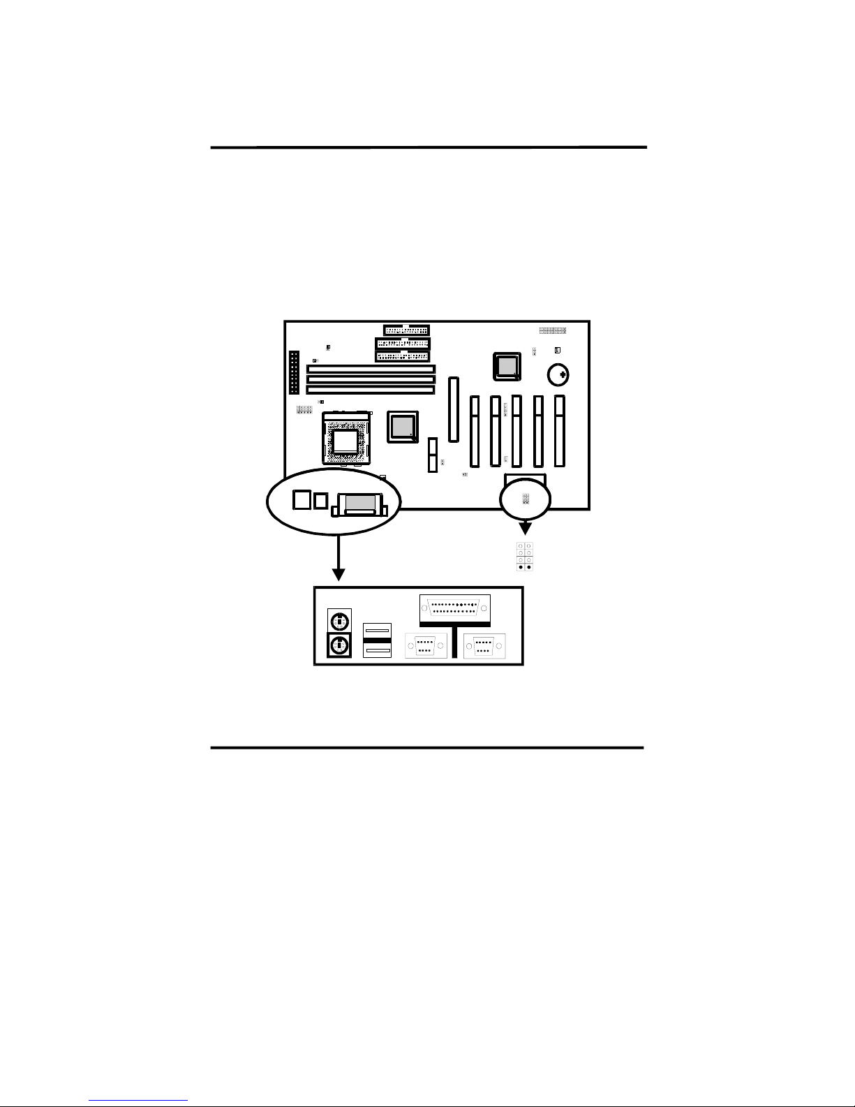
VIA694X System Board 17
2-3-2 Back Panel
There are keyboard/mouse, USB1/USB2, COM1/2, LPT1, port on the case back
panel. Please refer to more details as below.
KBMS1
USB1
COM1 COM2
LPT1
USB2
Page 24

VIA694X System Board 18
Keyboard & Mouse
The onboard PS/2 keyboard and mouse connectors are 6-pin Mini-Din
connectors, marked as “KEYBOARD” and “MOUSE.”
USB1/USB2(Universal Serial Bus)
Universal Serial Bus connector, marked as “USB,” is used to connect USB
devices. There are 4 USB connectors on this main board.
In Dos mode, USB2 doesn’t support “USB K/B support” function.
COM1/COM2
The onboard serial port 1 and port 2 are the 9-pin D-subminiature male
connector COM1/2. COM1/2 can be disabled in BIOS setup. Please refer to
Chapter 3 “Integrated Peripherals” for more information.
LPT1(Parallel Port)
The onboard parallel port is a 25-pin female connector, marked as “LPT.”
Page 25

VIA694X System Board 19
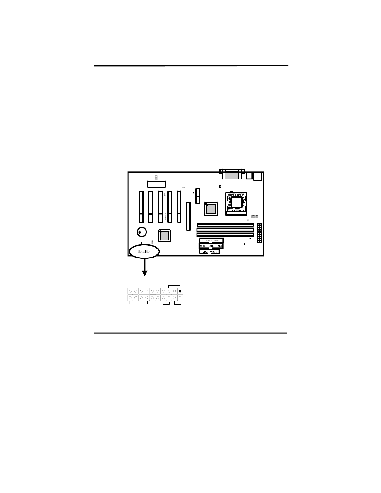
2-3-3 ATX Power Supply Connector
ATX power supply connector has 20 pins, which is designed for ATX case
especially. The ATX power supply supports the function of the “Soft Power On
Momentary switch” which connects on the front panel switch to the 2-pin
PW-BT on the system board. While the power switch on the back of ATX power
is turned on, the full power will not go into the system board until the front panel
switch is momentarily pressed. Push the switch again to turn off the power to the
system board.
Page 26

VIA694X System Board 20
2-3-4 CPU Fan Connectors
There are 2 fan connectors on this main board, and it is marked as “FAN1”,
“FAN2”. Each fan connector has three pins.
Fan Signal
SENSE
+12V
GND
FAN 1
FAN 2
Page 27

VIA694X System Board 21
2-3-5 I.R. : IrDA Connector
IR1 connector supports wireless infrared module. With this module and
application software like Laplink, or Win95 Direct Cable Connection, user can
transfer data to or from laptops, notebooks, PDA and printers. This connector
supports HPSIR, ASKIR, and Fast IR.
Attach Infrared module to IR connector. Be sure to put in the right direction
during installation.
I.R.:IrDA
Cinnector
Pin1
IR1
1
VCC
2
NONE
3
IRRX
4
GND
5
IRTX
Page 28

VIA694X System Board 22
2-3-6 Floppy Disk Connector
Floppy Disk Connector has 34 pins and is used to attach the floppy drive cable.
FDD1
Page 29

VIA694X System Board 23
2-3-7 IDE1 & IDE2
IDE1 and IDE2 are 40-pin IDE connectors. There are 2 IDE connectors
supported on this system board. IDE1 is primary channel, and IDE2 is secondary
channel. Each channel supports 2 IDE devices, and 4 devices in total for this main
board. It also supports Ultra DMA33/66 function.
IDE2
IDE1
Page 30

VIA694X System Board 24
2-4 DIMM Memory Installation
The main board has 3 DIMMs on board. Either DIMM1, DIMM2 or DIMM3
supports 8 MB, 16 MB, 32 MB, 64 MB, and 128MB. Maximum memory for
SDRAM is up to 256MB.
DIMM3
DIMM2
DIMM1
Page 31

VIA694X System Board 25
Insert the module as shown. Due to different number of pins on either side of the
breaks, the module will only fit in the orientation as shown. There is no jumper
setting for memory configuration.
DIMM
This main board supports both synchronous and asynchronous mode DIMMs.
User can use either PC-100 or PC-133 DIMMs.
Page 32

VIA694X System Board 26
Chapter 3 PhoenixNet
TM
BIOS Porting Guide
3-1 Product Overview
PhoenixNet
TM
is an end-user content service that displays system configuration
during the power on of a Personal Computer, and delivers promotional icons to
the desktop.
PhonixNet delivers 1) one-click, easy access to the Internet, 2) offers from leading
Internet companies, and 3) anti-virus protection(Trend ChipAway Virus
TM
) as
well as other free offers.
Each of the components has specific functionality and the interactions between the
components and the effects that each has upon the other will be examined in this
document.
Page 33

VIA694X System Board 27
3-2 Graphical Launch Screen (GLS)
The first ROMSmarts component, GLS, displays a graphical screen to the user
early in the boot process, as the first image displayed on the screen. This display
remains on the screen throughout the normal BIOS initialization phase called
POST.
The GLS component will replace the old text-based POST with a full graphical
screen. The screen will display PC metrics such as CPU vendor, model and speed,
memory and hard disk size.
Page 34

VIA694X System Board 28
Chapter 4 BIOS Setup
4-1 Award BIOS CMOS Setup
The menu displays all the major selection items and allow user to select any of
shown item. The selection is made by moving cursor (press any direction key) to
the item and press <Enter> key. An on-line help message is displayed at the
bottom of the screen as cursor is moving to various items which provides user
better understanding of each function. When a selection is made, the menu of
selected item will appear. So the user can modify associated configuration
parameters.
Page 35

VIA694X System Board 29
4-1-1 Standard CMOS Setup
The ”Standard CMOS Setup” allows user to configure system setting such as
current date and time, type of hard disk drive installed in the system, floppy
drive type, and the type of display monitor. Memory size is auto detected by the
BIOS and displayed for your reference. When a field is highlighted (direction keys
to move cursor and <Enter> key to select). The entries in the field will be
changed by pressing <PageDown> or <PageUp> key or user can enter new data
directly from the keyboard.
Page 36

VIA694X System Board 30
Page 37

VIA694X System Board 31
Hard Disk Configurations
1.IDE HDD Auto-Detection
: press this item to Auto Detect the HDD type.
2.IDE Primary Master : select “AUTO” to detect the mode type
automatically. Select “None/Auto/Manual” users
have to redefine the following 4-8 items according
to HDD.
“NONE” means this item disabled.
3. ACCESS MODE : select "AUTO" to detect the mode type
automatically. If your hard disk supports the LBA
mode, select "LBA" or "LARGE". However, if
your hard disk cylinder is more than 1024 and does
not support the LBA function, you have to set at
"LARGE.” Select "NORMAL" if your hard disk
supporting cylinder is below 1024.
4. CYLS : the cylinder number of the hard disk.
5. HEAD : the read/write head number of hard disk. The range is from "1"
to "16".
6.PRECOMP: the cylinder number at which the disk drive changes the write
timing.
7.LANDZ : the cylinder number that the disk drive heads (read/write) are
seated when the disk drive is parked.
8.SECTOR : the sector number of each track defined on the hard disk. The
range is from "1" to "64".
Note1: if hard disk primary master/slave and secondary master/slave were set
to “auto”, the hard disk size and model will be auto detected on display during
POST.
Note2: "halt on" is to determine when to halt the system by the BIOS if error
occurred during POST.
Page 38

VIA694X System Board 32
4-1-2 Advanced BIOS Features
Menu below shows all of the manufacturer's default values of this main board.
Move the cursor by pressing <PageDown>/- or <PageUp>/+ key to modify the
parameters, press [F1] key to display help message of the selected item. This setup
program also provide 2 convenient ways to load the default parameter data from
BIOS [F6] and [F7] area if shown data is corrupted. This provides the system a
capability to recover from any possible error.
Page 39

VIA694X System Board 33
Virus Warning
:Enabled
:Disabled (default)
CPU Internal Cache
Enabled : enable L1 cache(default)
Disabled: disable L1 cache
External Cache
Enabled (default): enable L2 cache
Disabled: disable L2 cache
CPU L2 Cache ECC Checking
Enabled (default): enable L2 cache ECC checking
Disabled: disable L2 cache ECC checking
Quick Power On Self Test
This category speeds up power on self test.
Enabled (default) : BIOS will shorten or skip some check items.
Disabled: normal speed
First Boot Device
This category determines which drive the system searches first. System will
search in turn for floppy disk drive; then hard disk drive, and finally Floppy drive.
Default value is “FLOPPY”. Options are as below:
FLOPPY; LS120; HDD-0; SCSI; CDROM; HDD-1; HDD-2; HDD-3;
ZIP100; LAN; Disabled
Page 40

VIA694X System Board 34
Second Boot Device
This category determines which drive the system searches first. System will
search in turn for floppy disk drive; then hard disk drive, and finally Floppy drive.
Default value is “HDD-0”. Options are as below:
FLOPPY; LS120; HDD-0; SCSI; CDROM; HDD-1; HDD-2; HDD-3;
ZIP100; LAN; Disabled
Third Boot Device
This category determines which drive the system searches first. System will
search in turn for floppy disk drive; then hard disk drive, and finally Floppy drive.
Default value is “LS120”. Options are as below:
FLOPPY; LS120; HDD-0; SCSI; CDROM; HDD-1; HDD-2; HDD-3;
ZIP100; LAN; Disable
Boot other Device
:Enabled (default)
:Disabled
Swap Floppy Drive
Enabled: floppy A&B will be swapped.
Disabled(default): floppy A&B will not be swapped.
Boot Up Floppy Seek
BIOS will determine if the floppy disk drive is 40 or 80 tracks. 360k type is 40
tracks while 720K/1.2M and 1.44M are all 80 tracks. Default value is Disabled.
Boot Up Numlock Status
:On(default)
:Off
Gate A20 Speed
:Normal
:Fast(default)
Page 41

VIA694X System Board 35
Typematic Rate Setting
This determines the typematic rate.
Enabled: enable typematic rate and typematic delay programming.
Disabled (default) : disable typematic rate and typematic delay programming. The
system BIOS will use default value of this 2 items and the default is controlled by
keyboard.
Typematic Rate(Chars/Sec)
6 : 6 Characters Per Second (default)
8 : 8 Characters Per Second
10 :10 Characters Per Second
12 : 12 Characters Per Second
15 : 15 Characters Per Second
20 : 20 Characters Per Second
24 : 24 Characters Per Second
30 : 30 Characters Per Second
Typematic Delay (Msec)
This is the interval between the first and second character displayed.
250 : 250 msec (default)
500 : 500 msec
750 : 750 msec
1000 :1000 msec
Security Option
Item Function Note
Setup (default) Security protection
in CMOS setup
menu
After setting password in BIOS CMOS
“Supervisor Password” or User
Password,” it protects BIOS CMOS setup.
System Security protection
in system boot-up
& BIOS setup
This function secures the system under
system boot-up and BIOS setup after setting
password.
Page 42

VIA694X System Board 36
OS Select For DRAM> 64MB
This option is especially set for OS2 operating system. Set “OS2” for RAM
memory over 64MB and set “Non-OS2” for other operating systems like
Windows® 95/98 or NT.
:Non-OS2(default)
:OS2
HDD S.M.A.R.T. Capability
:Disabled(default)
:Enabled
Video BIOS Shadow
To determine whether video BIOS will be copied to RAM for faster execution.
:Enabled(default)--- Video Shadow is enabled.
:Disabled --- Video Shadow is disabled.
C8000-CBFFF Shadow/DC000-DFFFF Shadow
These are categories determining whether optional ROM will be copied to RAM
by 16KB or 32KB per unit and the size depends on chipset.
:Enabled
:Disabled(default)
Page 43

VIA694X System Board 37
4-1-3 Advanced Chipset Features
Bank 0/1(2/3, 4/5) DRAM Timing
This will determine the timing of SDRAM. The user can separately adjust the
timing of bank 0/1, 2/3, 4/5.
: SDRAM 8/10ns (default)—10
nano second
: SDRAM 8ns, normal, medium, fast, turbo
Page 44

VIA694X System Board 38
SDRAM Cycle Length: control the DRAM page missing and row miss leadoff
timing.
:2
:3 (default)
DRAM Clock
:Host CLK (default)
System shows the actual DRAM speed the system uses.
:HCLK+33M
Please check DRAM clock for optimizes selection.
Memory Hole : this field enable a memory hole in main memory space. CPU
cycles matching an enabled hold are passed on to PCI note that a selected can not
be changed while the L2 cache is enabled.
:Disabled (default)
:15M-16M
P2C/C2P Concurrency
:Enabled (default)
:Disabled
Fast R-W Turn Around
:Enabled
:Disabled (default)
System BIOS Cacheable
:Enabled (default)
:Disabled
Video RAM Cacheable
:Enabled(default) --- allows caching of the video RAM, resulting in better system
performance. However, if any program writes to this memory area, a system error
may occur.
:Disabled
Page 45

VIA694X System Board 39
AGP Aperture Size
To select the size of the Accelerated Graphics Port (AGP) aperture is a portion of
the PCI memory address range dedicated for graphics memory address space.
Host cycles that hit the aperture range are forwarded to the AGP without any
translation.
:128M (default)
:64M, 32M, 16M, 8M, 4M
AGP-4X Mode
:Enabled (default)
:Disabled
AGP Driving Control
:Auto (default)
:Manual
AGP Driving Value
:Min:0000
:Max:00FF
Key in a Hex mumber:_______
AGP Fast Write
:Enabled
:Disabled(default)
OnChip USB
:Enabled (default)
Enabling this function adds the function of “USB Keyboard Support.”
:Disabled
OnChip USB2
:Enabled
:Disabled (default)
USB Keyboard Support
:Enabled--- enable this function when using USB keyboard in DOS mode.
Page 46

VIA694X System Board 40
:Disabled (default)
On Chip Sound
:
Auto
On Chip Modem
:
Auto
CPU to PCI Write Buffer
:Enabled (default)
:Disabled
PCI Dynamic Bursting
:Enabled (default)
:Disabled
PCI Master 0 WS Write
:Enabled (default)
:Disabled
PCI Delay Transaction
:Enabled (default)
:Disabled
PCI#2 Access #1 Retry
:Enabled (default)
:Disabled
AGP Master 1 WS Write
:Enabled
:Disabled (default)
AGP Master 1 WS Read
:Enabled
:Disabled (default)
Memory Parity/ECC Check
:Enabled --- enabled adds a parity check to the boot-up memory tests. Select
enabled only if the system DRAM contains parity.
:Disabled (default)
Page 47

VIA694X System Board 41
4-1-4 Integrated Peripherals
OnChip IDE Channel0/1
:Enabled (default)
:Disabled
IDE Prefetch Mode
:Enabled (default)
:Disabled
Page 48

VIA694X System Board 42
Primary Master PIO/ Primary Slave PIO
This feature detects your primary master hard disk device.
:Auto (default)
:Mode 0,1,2,3,4
Secondary Master PIO/Secondary Slave PIO
This feature detects your secondary master hard disk device.
:Auto (default)
:Mode 0,1,2,3,4
Primary Master UDMA/Primary Slave UDMA
:Auto (default)
:Disabled
Secondary Master UDMA/Secondary Slave UDMA
:Auto (default)
:Disabled
Init Display First
:AGP (default)
:PCI Slot
IDE HDD Block Mode
:Enabled (default)
:Disabled
Onboard FDD Controller
:Enabled (default)
:Disabled
Page 49

VIA694X System Board 43
Onboard Serial Port 1/Port 2
:3F8/IRQ4
:2F8/IRQ3
:3E8/IRQ4
:2E8/IRQ3
:Auto (default)
:Disabled
UART 2 Mode
:Standard (default) --- the user is not allowed to modify “IR Function Duplex,”
and “TX, RX inverting enable.”
:ASKIR --- the user is allowed to modify “IR Function Duplex,” and “TX, RX
inverting enable.”
:HPSIR --- the user is allowed to modify “IR Function Duplex,” and “TX, RX
inverting enable.”
Onboard Parallel Port
:378/IRQ7 (default)
:278H/IRQ5
:3BC/IRQ7
:Disabled
Onboard Parallel Mode
:Normal (default)
:ECP, EPP, ECP/EPP
ECP Mode Use DMA
Select a DMA channel for the parallel port for use during ECP mode.
:3 (default)
:1
Parallel Port EPP Type
This item allows you to determine the IR transfer mode of onboard I/O chip.
:EPP1.9 (default)
:EPP1.7
Page 50

VIA694X System Board 44
Onboard Legacy Audio
:Disabled
:Enabled
Sound Blaster
:Disabled
:Enabled
SB I/O Base Address
:220H
:240H
:260H
:280H
SB IRQ Select
:IRQ5
:IRQ7
:IRQ9
:IRQ10
SB DMA Select
:DMA0
:DMA1
:DMA2
:DMA3
MPU401
:Disabled
:Enabled
MPU401 I/O ADDRESS
:300-303H
:310-313H
:320-323H
:330-333H(Default)
Page 51

VIA694X System Board 45
Game Part
(
200-207h)
:enabled
Page 52

VIA694X System Board 46
4-1-5 Power Management Setup
ACPI function
This function allows you to enable/disable the Advanced Configuration and Power
Management(ACPI).
:Enabled (default)
:Disabled
ACPI Suspend Type
:S1(POS) (default)
PM Control By APM
No : system BIOS will ignore APM
Ye s (default) : system BIOS will wait for APM’s prompt before it enter any PM
mode, eg. Doze, standby or suspend.
Page 53

VIA694X System Board 47
Note1: If APM is installed, and there is a task running, even if the timer
is time out, the APM will not prompt the BIOS to put the system into any
power saving mode.
Note2: If APM is not installed, this option has no effect.
Video Off Option
:Suspend --> Off(default)
:All Modes --> Off
:Always On
Video Off Method
This item determines the manner in which the monitor is blanked.
:V/H SYNC+Blank(default) --- this selection will cause the system to turn off the
vertical and horizontal synchronization ports and write blanks to the video buffer.
:Blank Screen --- this option only writes blanks to the video buffer.
:DPMS Support --- Initial display power management signaling.
MODEM Use IRQ
:3(default)
:4, 5, 7, 9, 10, 11, NA
Soft-Off by PWRBTN
:Instant-off (default)
:Delay 4 sec
This allows the user to set the soft-off power button to turn off the system or set to
“4 seconds” holding the power and system will shut down in 4 seconds.
State After Power Failure
This field lets you determine the state that your PC returns to after a power
failure.
:Auto
:On --- the PC will restart after a power failure.
:Off(default) --- the PC will not boot after a power failure.
Page 54

VIA694X System Board 48
Power Management
:User Define(default)--users can configure their own power management
:Min Saving
:Max Saving
HDD Power Down
When enabled and after the set time of system inactivity, the hard disk drive will
be powered down while all other devices remain active.
:Disabled(default)
:1 Min ∼ 15 Min
Doze Mode
:Disabled(default)
:1 Min, 2 Min, 4 Min, 6 Min, 8 Min, 10 Min, 20 Min, 30 Min, 40 Min, 1 hour.
Suspend Mode
:Disabled(default)
:1 Min, 2 Min, 4 Min, 6 Min, 8 Min, 10 Min, 20 Min, 30 Min, 40 Min, 1 hour.
Page 55

VIA694X System Board 49
VGA
:ON
:OFF(default)
LPT & COM
:LPT/COM (default)
:NONE
:LPT
:COM
HDD & FDD
:ON(default)
:OFF
PCI Master
:ON
:OFF(default)
Page 56

VIA694X System Board 50
Modem Ring Resume
Enabled: modem ring on function --- system can be turned on through modem.
Disabled(default): disble this function.
Note: this function only works when the system is turned off from Windows
mode, and Doze mode will not function.
RTC Alarm Resume: auto power on at the appointed date and time.
Enabled: key in the date of current month and time of the day. System will turn
on then.
Disabled (default): disable this function.
Note: this function only works when the system is turned off.
Primary INIR
IRQ Activity Monitoring
Page 57

VIA694X System Board 51
Primary INTR
:ON (default)
Select “on,” it adds the following functions, “IRQ3(COM2) - IRQ15
(Reserved).”
:OFF
Select “off,” “IRQ3 (COM2)- IRQ15 (Reserved)” will not show.
Page 58

VIA694X System Board 52
4-1-6 PnP/PCI Configuration Setup
Page 59

VIA694X System Board 53
PNP OS Installed
:No(default)
OS will not recognize PnP devices.
:Yes
OS will arrange the setup of PnP devices.
Reset Configuration Data
:Disabled(default)
:Enabled --- to reset “Extended System Configuration Data(ESCD) when you
exit setup if you have installed a new add-on card and the system reconfiguration
has caused such a serious conflict that the operating system can not boot up.
Resources Controlled By
:Manual
The table will show the below items: “IRQ Resources, DMA Resources.” The
user can adjust the shown items as required.
:Auto(ESCD) (default)
The table will not show the above items, and the system will automatically assign
the above setup.
PCI/VGA Palette Snoop
:Enabled
:Disabled (default)
Assign IRQ For VGA
:Enabled (default)
:Disabled
Assign IRQ For USB
:Enabled (default)
:Disabled
Page 60

VIA694X System Board 54
4-1-7 PC Health Status
Current CPU Temperature, Current CPU Fan1 speed/CPU Fan2 speed/Current
Vin3(V)/Vin1(V)/VIN(2)/Vdd(V):
System will automatically detect the above items and show the status.
Page 61

VIA694X System Board 55
4-1-8 Frequency/Voltage Control
Auto Detect DIMM/PCI CIK
:Enabled
:Disabled (default)
Spread Spectrum
:0.25%
:0.50%
:Disabled(default)
This selection is reserved for manufacturers to pass CE test only not available
for users.
CPU Host Clock (CPU/PCI)
: 66/33 MHz, 75/37 MHz, 83/41 MHz, 100/33 MHz, 103/34 MHz, 112/37 MHz,
124/41 MHz, 133/44 MHz, 124/31 MHz, 133/33 MHz, 140/35 MHz
Page 62

VIA694X System Board 56
4-1-9 Load Optimized Defaults
"Load Optimized Defaults" loads optimized settings which are stored in the
BIOS ROM. The auto-configured settings only affect “BIOS Features Setup”
and “Chipset Features Setup” screens. There is no effect on the standard CMOS
setup. To use this feature, highlight it on the main screen and press the <Enter>
key. A line will appear on screen asking if you want to load the setup default
values. Press the <Y> key and then press the <Enter> key. The setup defaults will
then load. If not, enter <N>.
Page 63

VIA694X System Board 57
4-1-10 Supervisor/User Password
The "Supervisor/User Password setting" utility sets the security protection.
There are two kinds of password functions in the setup menu : one is “Supervisor
Password,” and the other is “User Password.” Their difference is:
Supervisor Password: this function allows you the right to change the options of
setup menu.
User Password: this function only allows you to enter the setup menu but not to
change the options of the setup menu except “USER PASSWORD,” “SAVE &
EXIT SETUP,” and “EXIT WITHOUT SAVING.”
1. How to set “Supervisor Password” & “User Password”
The setup of “Supervisor Password” and “User Password” has the same steps.
Step 1: Enter Password --Press <Enter> after appointing the password.
Page 64

VIA694X System Board 58
Step 2 : Confirm Password
Type the password again and press <Enter>.
If you forget password, please clear CMOS.
(refer to jumper JBAT)
Step 3: Set “Security Option” in “BIOS Features Setup”
After setting password, enter “Security Option” in “BIOS Features Setup.”
There are 2 options “Setup” & “System.” “Setup” will only secure CMOS setup
through password. “System” is to secure PC sytem and password is required
during system boot-up in addition to CMOS setup.
Page 65

VIA694X System Board 59
2. How to Disable “Supervisor Password” & “User Password”.
Step 1: Go to CMOS Setup Menu (need to key in password first)
Step 2: Enter “Supervisor Password” or “User Password”
When it shows “Enter Password”, press the <Enter> key instead of entering a new
password when "ENTER PASSWORD" appears. It will inform “PASSWORD
DISABLED PRESS ANY KEY TO CONTINUNE.” Then, press any key as
instructed to disable the password.
Page 66

VIA694X System Board 60
4-1-11 Save & Exit Setup
The "Save & Exit Setup" option will bring you back to boot up procedure with
all the changes you have made which are recorded in the CMOS RAM.
Page 67

VIA694X System Board 61
4-1-12 Quit Without Saving
The "Quit Without Saving" option will bring you back to normal boot up
procedure without saving any data into CMOS RAM. All of the old data in the
CMOS will not be changed.
Page 68

VIA694X System Board 62
Chapter 5 Appendix
5-1 Memory Map
Address range Size Description
00000-7FFFF 512K Conventional memory
80000-9FBFF 127K Extended conventional memory
9FC00-9FFFF 1K Extended BIOS data area if PS/2 mouse is
installed
A0000-C7FFF 160K Available for hi DOS memory
C8000-DFFFF 96K Available for hi DOS memory and adapter
ROMs
E0000-EEFFF 60K Available for UMB
EF000-EFFFF 4K Video service routine for monochrome &
CGA adapter
F0000-F7FFF 32K BIOS CMOS setup utility
F8000-FCFFF 20K BIOS runtime service routine (2)
FD000-FDFFF 4K Plug and play escd data area
FE000-FFFFF 8K BIOS runtime service routine (1)
Page 69

VIA694X System Board 63
5-2 I/O Map
000-01F DMA controller (master)
020-021 Interrupt controller (master)
022-023 Chipset control registers. I/O ports
040-05F Timer control registers
060-06F Keyboard interface controller (8042)
070-07F RTC ports & CMOS I/O ports
080-09F DMA register
0A0-0BF Interrupt controller (slave)
0C0-0DF DMA controller (slave)
0F0-0FF Math coprocessor
1F0-1FB Hard disk controller
278-27F Parallel port 2
2B0-2DF Graphics adapter controller
2F8-2FF Serial port 2
360-36F Network ports
378-37F Parallel port 1
3B0-3BF Monochrome & parallel port adapter
3C0-3CF EGA adapter
3D0-CDF CGA adapter
3F0-3F7 Floppy disk controller
3F8-3FF Serial port-1
Page 70

VIA694X System Board 64
5-3 Time & DMA Channels Map
Time map:
Timer channel 0 system timer interrupt
Timer channel 1 DRAM refresh request
Timer channel 2 speaker tone generator
Dma channels:
DMA channel 0 available
DMA channel 1 onboard ECP (option)
DMA channel 2 floppy disk (ITE chip)
DMA channel 3 onboard ECP (default)
DMA channel 4 cascade for DMA controller 1
DMA channel 5 available
DMA channel 6 available
DMA channel 7 available
Page 71

VIA694X System Board 65
5-4 Interrupt Map
A. NMI: non-maskable interrupt
B. IRQ(H/W):
0 system timer interrupt from timer 0
1. 1 keyboard output buffer full
2. cascade for IRQ 8-15
3. serial port2
4. serial port1
5. parallel port 2
6. floppy disk (ITE chip)
7. parallel port 1
8. RTC clock
9. available
10. available
11. available
12. PS/2 mouse
13. math coprocessor
14. onboard hard disk (IDE1) channel
15. onboard hard disk (IDE2) channel
Page 72

VIA694X System Board 66
5-5 RTC & CMOS RAM Map
00 Seconds
01 Seconds Alarm
02 Minutes
03 Minutes Alarm
04 Hours
05 Hours Alarm
06 Day of Week
07 Day of Month
08 Month
09 Year
0A Status Register A
0B Status Register B
0C Status Register C
0D Status Register D
0E Diagnostic Status Byte
0F Shutdown Byte
10 Floppy Disk Type Drive Type Byte
12 Hard Disk Type Byte
13 Reserved
14 Equipment Type
15 Base Memory Low Byte
16 Base Memory High Byte
17 Extension Memory Low Byte
18 Extension Memory High Byte
19-2D
2E-2F
30 Reserved for Extension Memory Low Byte
31 Reserved for Extension Memory High Byte
33 Information Flag
34-3F Reserved
40-7F Reserved for Chipset Setting Data
Page 73

VIA694X System Board 67
5-6 Award BIOS Hard Disk Type
Type Cylinder Heads Write
Pre-comp
Landing
Zone
Sectors Size
1 306 4 128 305 17 10MB
2 615 4 300 615 17 21MB
3 615 6 300 615 17 32MB
4 940 8 512 940 17 65MB
5 940 6 512 940 17 49MB
6 615 4 65535 615 17 21MB
7 462 8 256 511 17 32MB
8 733 5 65535 733 17 31MB
9 900 15 65535 901 17 117MB
10 820 3 65535 820 17 21MB
11 855 5 65535 855 17 37MB
12 855 7 65535 855 17 52MB
13 306 8 128 319 17 21MB
14 733 7 65535 733 17 44MB
16 612 4 0 663 17 21MB
17 977 5 300 977 17 42MB
18 977 7 65535 977 17 59MB
19 1024 7 512 1023 17 62MB
20 733 5 300 732 17 31MB
21 733 7 300 732 17 44MB
22 733 5 300 733 17 31MB
23 306 4 0 336 17 10MB
24 977 5 0 925 17 42MB
25 1024 9 65535 925 17 80MB
26 1224 7 65535 754 17 74MB
Page 74

VIA694X System Board 68
Type Cylinder Heads Write
Pre-comp
Landing
Zone
Sectors Size
27 1224 11 65535 754 17 117MB
28 1224 15 65535 699 17 159MB
29 1024 8 65535 823 17 71MB
30 1024 11 65535 1023 17 98MB
31 918 11 65535 1023 17 87MB
32 925 9 65535 926 17 72MB
33 1024 10 65535 1023 17 89MB
34 1024 12 65535 1023 17 106MB
35 1024 13 65535 1023 17 115MB
36 1024 14 65535 1023 17 124MB
37 1024 2 65535 1023 17 17MB
38 1024 16 65535 1023 17 142MB
39 918 15 65535 1023 17 119MB
40 820 6 65535 820 17 42MB
41 1024 5 65535 1023 17 44MB
42 1024 8 65535 1023 17 68MB
43 809 6 65535 852 17 42MB
44 809 9 65535 852 17 64MB
45 776 8 65535 775 17 104MB
46 AUTO 0 0 0 0
47 USER’S TYPE
Page 75

VIA694X System Board 69
5-7 ISA I/O Address Map
I/O Address (HEX)
I/O device
000 - 01F DMA Controller 1, 8237A-5
020 - 03F Interrupt Controller 1, 8259A
040 - 05F System Timer, 8254-2
060 - 06F 8042 Keyboard Controller
070 - 07F real-time Clock/CMOS and NMI Mask
080 - 09F DMA Page Register, 74LS612
0A0 - 0BF Interrupt Controller 2, 8259A
0C0 - 0DF DMA Controller 2, 8237A-5
0F0 - 0FF i486 Math Coprocessor
1F0 - 1F8 Fixed Disk Drive Adapter
200 - 207 Game I/O
20C - 20D Reserved
21F Reserved
278 - 27F Parallel Printer Port 2
2B0 - 2DF Alternate Enhanced Graphic Adapter
2E1 GPIB Adapter 0
2E2 - 2E3 Data Acquisition Adapter 0
2F8 - 2FF Serial Port 2 (RS-232-C)
300 - 31F Prototype Card
360 - 363 PC Network (Low Address)
364 - 367 Reserved
368 - 36B PC Network (High Address)
36C - 36F Reserved
378 - 37F Parallel Printer Port 1
Page 76

VIA694X System Board 70
I/O Address (HEX)
I/O device
380 - 38F SDLC, Bisynchronous 2
390 - 393 Cluster
3A0 - 3AF Bisynchronous 1
3B0 - 3BF Monochrome Display and Printer Adapter
3C0 - 3CF Enhanced Graphics Adapter
3D0 - 3DF Color/Graphics Monitor Adapter
3F0 - 3F7 Diskette Drive Controller
3F8 - 3FF Serial Port 1 (RS-232-C)
6E2 - 6E3 Data Acquisition Adapter 1
790 - 793 Cluster Adapter 1
AE2 - AE3 Data Acquisition Adapter 2
B90 - B93 Cluster Adapter 2
EE2 - EE3 Data Acquisition Adapter 3
1390 - 1393 Cluster Adapter 3
22E1 GPIB Adapter 1
2390 - 2393 Cluster Adapter 4
42E1 GPIB Adapter 2
62E1 GPIB Adapter 3
82E1 GPIB Adapter 4
A2E1 GPIB Adapter 5
C2E1 GPIB Adapter 6
E2E1 GPIB Adapter 7
Page 77

VIA694X System Board 71
Chapter 6 Q & A
6-1 Error Messages During Power on Self Test
During power on self test (post), BIOS will automatically detect the system
devices. Below are the questions that users most often meet. The user may press
“Esc” key to skip the full memory test.
1. Beep sound
On power on, the system make beep sound to offer different messages. If the
system is configured correctly, it prompts a short beep to show device
configuration is done correctly. When VGA card and DIMM modules are not
plugged well, the system makes longer and constant beep sounds.
2. BIOS ROM checksum error
It indicates the checksum of the BIOS code is not right and system will always
halt on power on screen. Contact the dealer to exchange a new BIOS.
3. CMOS battery fails
It indicates the CMOS battery does not work. Contact the dealer to exchange a
new battery.
4. CMOS checksum error
It indicates the CMOS checksum is incorrect. Load the default values in BIOS to
solve this problem. This error may result from a weak BIOS, so replace a new
BIOS if necessary.
Page 78

VIA694X System Board 72
5. Hard disk initialize
Please wait a moment…
Some hard drives require more time to initialize.
6. Hard disk install failure
The system can not find or initialize the hard drive controller or the drive. Check
if the controller is set correctly. If no hard disk is installed, “Hard drive
selection” must be set to “none.”
7. Keyboard error or no keyboard present
This means the system can not initialize the keyboard. Check if the keyboard is
plugged well and be sure no keys are pressed during POST.
8. Keyboard is lock out - Unlock the key
When this message comes out, check if there is anything mis-placed on the
keyboard. Be sure nothing touches the keys.
9. Memory test fails
There will be more information to specify the type and location of the memory
error.
10 Primary master hard disk fail
The BIOS find an error in the primary master hard disk drive.
11 Primary slave hard disk fail
The BIOS finds an error in the primary slave hard disk drive.
12 Secondary master hard disk fail
The BIOS finds an error in the secondary slave master hard disk drive.
13 Secondary slave hard disk fail
The BIOS finds an error in the secondary slave IDE hard disk drive.
 Loading...