

Page 1

VT82C42
K
EYBOARD CONTROLLER
VIA TECHNOLOGIES, INC.
Preliminary Release
DATE : November 22, 1995
Page 2

P
RELIMINARY DOCUMENT RELEASE
The material in this document supersedes all previous documentation issued for any of the products
included herein. Please contact VIA Technologies for the latest documentation.
Copyright Notice:
©
Copyright
No part of this document may be reproduced, transmitted, transcribed, stored in a retrieval system, or
translated into any language, in any form or by any means, electronic, mechanical, magnetic, optical,
chemical, manual or otherwise without the prior written permission of Via Technologies Incorporated.
The VT82C42 may only be used to identify products of VIA Technologies.
All trademarks are the properties of their respective owners.
1995, Via Technologies Incorporated. Printed in Taiwan. A
LL RIGHTS RESERVED
.
Disclaimer Notice:
No license is granted, implied or otherwise, under any patent or patent rights of VIA Technologies . VIA
Technologies mak es no warranties, implied or otherwise, in regard to this document and to the products
described in this document. The information pr ovided by this document is believed to be accurate and
reliable to the publication date of this document. However, VIA Technologies assumes no responsibility for
any errors in this document. Furthermore, VIA Technologies assumes no responsibility for the use or
misuse of the infor mation in this document and for any patent infringem ents that may arise from the use of
this document. The information and pr oduct specifications within this docum ent are subject to change at
any time, without notice and without obligation to notify any person of such change.
Offices:
5020 Brandin Court 8th Floor, No. 533
Fremont, CA 94538 Chung-Cheng Rd., Hsin-Tien
USA Taipei, Taiwan ROC
Tel: (510) 683-3300 Tel: (886-2) 218-5452
Fax: (510) 683-3301 Fax: (886-2) 218-5453
Page 3

VIA Technologies, Inc.
VT82C42
VT82C42 Keyboard Controller
Date : November 22, 1995
1. General Overview:
The VT82C42 is a compatible direct replacement for the Intel 80C42 BIOS version of the Keyboard
Controller. The VT82C42 is fully implemented by hardware logic so that it has a very fast response capability
for any command issued by the host. In addition to keyboard support, the VT82C42 also offers PS/2 mouse
support. The VT82C42 also offers the Mouse Lock
designed by VIA technologies, which locks the mouse when the keylock function is initiated.
2. Features:
∗
Fully hardware implemented, 0.8µm CMOS Technology.
∗
Very high speed response of A20 GATE & reset.
∗
Support PS2 style mouse.
∗
Compatible with all major BIOS, including AWARD, PHOENIX and AMI.
TM
function (patent pending), a feature exclusively
∗
40 pin PDIP and 44 pin PLCC packages.
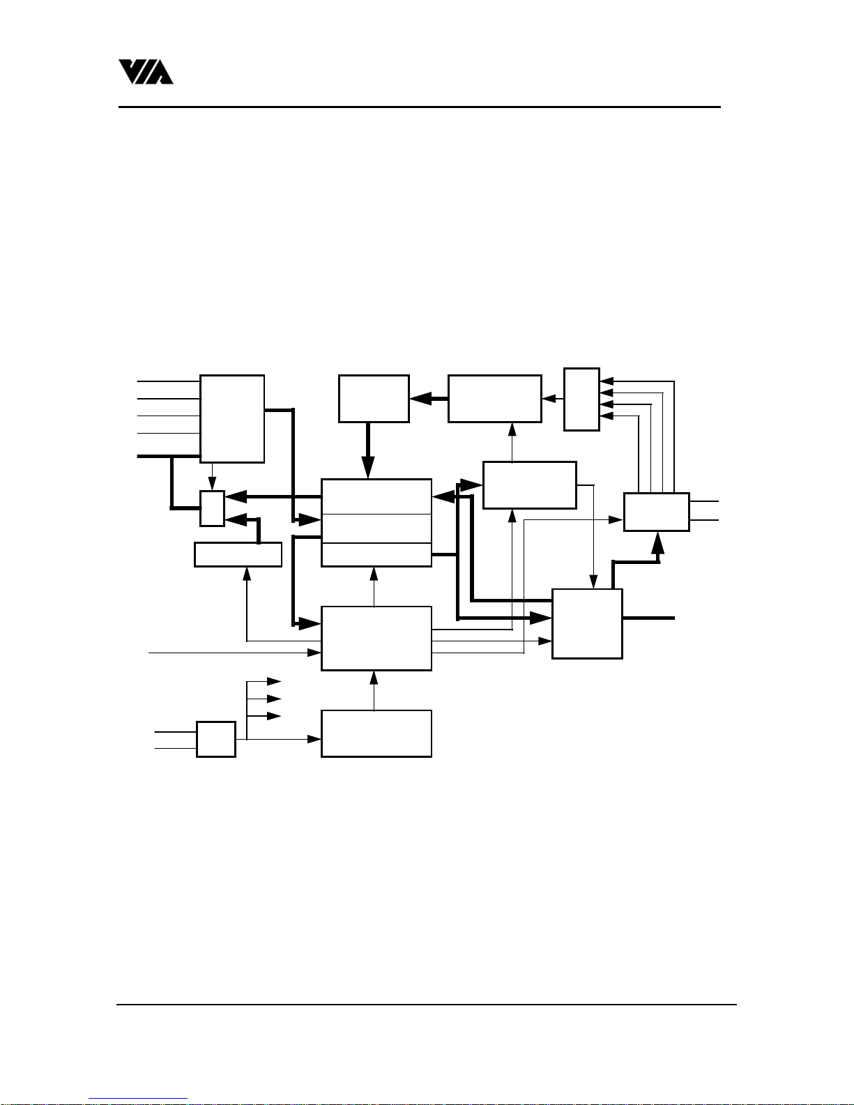
3. Function Description:
The internal timer counting is based on an 8Mhz clock input from X1, X2 ( or X2, with X1 connected to
ground). After the deassertion of RESET#, the VT82C4 2 will drive high at pin P 23 and pin P 2 7. After 6 µs (6
x 8 clocks) of driving, the VT82C42 will check on pins T1 & P10; if both pins are low, then the VT82C42
will switch to PS/2 mode. Otherwise, the VT82C42 will remain in AT mode.
If the VT82C42 is in AT mode after the self test, then it will drive P24 and P2 5 low with all other ports high.
If the VT82C42 is in PS/2 mode, then it will drive P24, P25, P 22, and P 27 low with all other ports high. The
VT82C42 will not change its driving value until it receives the command "AA" from the host. When receiving
the command "AA" from the host, the VT82C42 will prepare a "55" in its output buffer and drive P24
(reflecting the internal OBF flag) high within 6 clocks. This response time is the typical active time for
internal IBF flag. After this initialization procedure, the VT82C42 will drive P26 low (AT mode) or drive P26
and P23 low (PS/2 mode) in order for the keyboard and mouse interface to receive data from keyboard or
mouse.
When the keyboard or mouse toggles the interface (KBCLK, KBDATA, MSCLK,MSDATA), the controller
receives data from the serial interface and stores the received data into its internal output buffer. If the
received data is from the keyboard, a scan code translation is executed before the data is sent to the output
buffer. The VT82C42 also raises P24 or P25 to indicate a output buffer full. The host is signaled to issue a
read command to the data port to read the received data out. When the VT82C42 receives data in the normal
mode (pin 25 on DIP40 or pin 28 on PLCC44 parts connected to VCC) and the status of P17 is low, then the
controller will not raise the P24, nor activate its internal OBF flag. It looks like the contro ller will consume the
income data itself. And if the data is from the mouse, the controller will still raise P25 to indicate that data is
coming from mouse. However, if the VT82C42 is in Mouse Lock
PLCC44 parts connected to GND), the data from either keyboard or mouse will be prohibited from sending to
the host.
TM
mode (pin 25 on DIP40 or pin 28 on
-1-
Page 4
VIA Technologies, Inc.
VT82C42
The host can program the output port (P20-P23 in AT mode, or P20-P21 in PS/2 mode) or in-out port (P10P15 in AT mode, or P12-P15 in PS/2 mode) by issuing a command to the command register on the VT82C42.
The controller will then quickly execute the specified command. Note that P16-P17 is implemented as an
input port only. The host can also transmit data to the keyboard and mouse by issuing a command to the data
register. The data coming to the data register (with A0 = 0, CS# = 0, RD# = 1, and WR# = 0) will be sent to
the keyboard via the keyboard serial interfaces. The data sent to the mouse will be completed by 1) issuing a
D4 command to the command register, 2) then writing the following data byte to the data register (to be sent to
the mouse via mouse serial interface). In either case, the VT82C42 will wait for an acknowledgement from the
keyboard or mouse to complete a transmission. At the same time as the completion of the transmission, the
VT82C42 will raise P24 or P25 (when sending data to mouse) to signal the host of a completion of
transmission. When the controller receives or transmits, the controller does a parity and time-out check. If any
error occurs in the interface or inside the external devices (keyboard or mouse), the controller will reflect that
error in the following status register.
A0
C S
IOR
IOW
D[7: 0]
command
decoder
scan
mappi ng
rece iving u nit
debounci ng
KBCK
KBDT
MSCK
MSDT
RES ET
X1, X2
+
status register
cl ocking
(8 Mhz)
data input buffer
transmitting u nit
command reg ister/
data register
data output buffer
arbitration &
cent r al co ntrol
unit
tim e r
Fig 1. Block Diagram for VT82C42
In/Out
por t buf fer
mode
selector
P[17:10]
P[27:20]
T1
T0
-2-
Page 5

VIA Technologies, Inc.
VT82C42
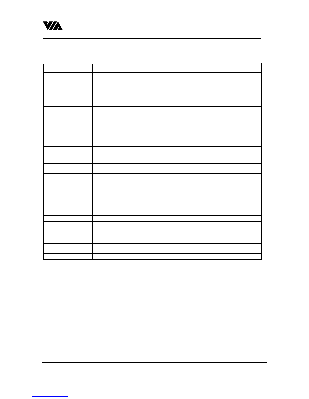
4. Register
Table 1. Status register: read only (with A0 = 1, CS# = 0, RD# = 0, WR# = 1)
Bit0 : OBF 1 means output buffer is full, 0 means output buffer is empty.
Bit1 : IBF 1 means input buffer is full, 0 means input buffer is empty.
Bit2 : system flag 0 after power on
Bit3 : command/Data 1 means last write is command write. 0 means last write is data write.
Bit4 : keylock status To represent the inhibition of keyboard. 0 means keyboard is inhibited. 1
means keyboard is not inhibited.
Bit5 : transmit timeout/mouse OBF
Bit6 : receive timeout/general time-out
Bit7 : parity error 1 means even parity has occurred in the last transmit/receive.
Table 2. Command register: read/write (use command 20h/60h)
Bit0 : OBF enable 1 means controller will generate high (interrupt) on P24 when output buffer
Bit1 : mouse OBF enable 1 means controller will generate high (interrupt) on P25 when mouse data
Bit2 : system flag Connect to the status register Bit2.
Bit3 : inhibit override Write a '1' to this Bit will disable the keyboard inhibit function.
Bit4 : prohibit enabling of
keyboard interface
Bit5 : IBM PC keyboard
type protocol/disable
mouse interface
Bit6 : PC compatible mode Default is 1, means the scan code translation is on.
Bit7 : reserved.
Act as transmit time-out on AT mode. 1 means error happens. Act as Mouse
OBF on PS2 mode. 1 means mouse output buffer full.
Act as receive time-out on AT mode. 1 means error happens. Act as general
(receive/transmit) time-out on PS2 mode.
has been written.
comes in output buffer.
Write a '1' to this Bit will disable keyboard interface
On AT mode, 0 means that the controller will do a IBM keyboard like
checking on receiving. On PS2 mode, a '1' disable the mouse interface
Table 3. Command List: (with A0 = 1, CS# = 0, RD# = 1, WR# = 0)
20h : read command byte
register.
60h : write command byte
register.
9xh : write low nibble to
(Port13-Port10).
A1h : controller's version
number.
A4h : check password
command
A7h : disable mouse
interface
A8h : enable mouse
interface
A9h : mouse interface test. Return 00h if the interface is O.K..
AAh : controller's self test Return 55h if the controller is O.K..
ABh : keyboard interface
test.
ADh : disable keyboard
interface.
AEh : enable keyboard
interface.
AFh : return version
After command execution, OBF = 1 means data is ready on the output
buffer.
Next byte write to Data port will be written to command byte register.
After command execution, OBF = 1 means data is ready on the output
buffer.
Always return 'F1' on output buffer.
After the command execution, Command byte register bit5 = 1 and P23 = 1
on PS2 mode. No effect on AT mode.
After the command execution, Command byte register bit5 = 0 and P23 = 0
on PS2 mode. No effect on AT mode.
Return 00h if the interface is O.K..
-3-
Page 6

VIA Technologies, Inc.
VT82C42
number.
B0h : write 0 to P10.
B1h : write 0 to P11.
B2h : write 0 to P12.
B3h : write 0 to P13.
B4h : write 0 to P22.
B5h : write 0 to P23.
B6h : write 0 to P14.
B7h : write 0 to P15.
B8h : write 1 to P10.
B9h : write 1 to P11.
BAh : write 1 to P12.
BBh : write 1 to P13.
BCh : write 1 to P22.
BDh : write 1 to P23.
BEh : write 1 to P14.
BFh : write 1 to P15.
C0h : read controller's
input ports P17-P10.
C1h : poll input port
low.
C2h : poll input port
high.
C8h : enable D1
command be effective
to P22 and P23.
C9h : disable D1
command be effective
to P22 and P23.
CAh : return on bit0 the
mode value.
D0h : return the
controller's output port
P20-P27.
D1h : write output port. The next byte written to data port will be put on output port.
D2h : write keyboard
output buffer
D3h : write mouse
output buffer
D4h : write to mouse The next byte written in to data port will be transmit to mouse.
E0h : read test inputs. Return T0 & T1 values on bit0 & bit1 respectively.
Exh : active output
ports
Fxh : pulse output ports P23-P20 will be pulse low for 6us according to the status on bit3-
Read from P11,P12,P13 and write to status register bit5,bit6,bit7.
Read from P15,P16,P17 and write to status register bit5,bit6,bit7.
1 for PS2 mode, 0 for AT mode.
The next byte written in to data port will be put on the output buffer
and OBF = 1.
The next byte written in to data port will be put on the output buffer
and mouse OBF = 1.
P23-P21 will change according to the status on bit3-bit1.
bit0.
5. Design Example:
1. To work with AT mode mother board.
-4-
Page 7

VIA Technologies, Inc.
VT82C42
T0
7406
P26
Keyboard Clock
T1
P27
7407
Fig 2.
2. To work with PS2 mode mother board.
P10
T0
T1
P11
P22
P27
P26
7406
7406
7406
Keyboard Data
Mouse Data
Keyboard Data
Keyboard Clock
P23
7406
Mouse Clock
Fig 3.
-5-
Page 8
VIA Technologies, Inc.
VT82C42
6. VT82C42 Signal Description
Table 4. Signal Description for VT82C42
Symbol 40-Pin 44-Pin Type Name and Function
D0-D
(BUS)
P10-P
13
P20-P
27
P14-P
15
P16-P
17
WR# 10 11 I Act as a write signal.
RD# 8 9 I Act as a read signal.
CS# 6 7 I Chip select of this chip.
A
0
12-19 14-20 I/O Act as data input or data output.
7
27-30 30-33 I/O Pullup open drain port. Writing a '1' to these ports tri-states the
ports. Act as input 'high' simultaneously if no outside 'low'
connection. Writing a '0' to these ports results in generating a low
on the port.
21-24
35-38
31, 32 35, 36 I/O Pullup open drain port. Writing a '1' to these ports tri-states the
33, 34 37, 38 I Input port 16, Input port 17
9 10 I Command/Data select when RD# or WR# is active.
24-27
39-42
Output Port 20 - Output Port 23
O
Output Port 24 - Output Port 27
ports. Act as input 'high' simultaneously if no outside 'low'
connection. Writing a '0' to these ports results in generating a low
on the port.
TEST 0,
TEST 1
XTAL 1,
XTAL 2
TH_SS
TH_PROG
TH_SSPP
TL_EA 7 8 I Tie to ground.
SYNC 11 12 O Internal state synchronous output.
NC 1, 13, 23,
RESET# 4 5 I A low in this pin reset the chip to a known state.
V
CC
GND 20 22 Ground.
1
39
2
3
5
25
26
40 44 Power supply of 4.5 to 5.5v.
43
28
29
34
2
3
4
6
I Act as Keyboard clock input in both AT mode & PS2 mode
Act as Keyboard Data input in AT mode. Act as Mouse Clock
input in PS2 mode.
I Act as clock input to the chips. Can be connected to LC circuit or
a single clock source (X2).
I Tie to VCC
I No connection.
1. Description for Table 4
RESET# is active low and is only an input pin. VT82C42 requires 10 clocks before RESET# goes to high to
have the chip go to a known state.
Pins WR#, RD#, CS# and A
are all input only pins and must activate for at least one clock cycle width to be
o
recognised by the VT82C42.
D
are two-way pins, each having 4mA TTL compatible output driving. When D0-D7 is provided by the
0-d7
host, write cycle data should cover all the WR# CS# A
VT82C42, the D
is available as long as the RD#=0 CS#=0 command is asserted and is held one clock
0-D7
command width. When the D0-D7 is provided by the
0
cycle after the command is deasserted.
TEST0,TEST1 are input only pins. TEST0 is expected to connect to KBCLK no matter what mode the
VT82C42 is in. TEST1 is expected to connect to KBDATA when in AT-mode, and is expected to connect to
MSCLK when in PS/2 mode. They have a 50K ohm pull up internally.
-6-
Page 9

VIA Technologies, Inc.
VT82C42
P16,P17 are input only pins. They have a 50K ohm pull up internally.
P20-P26 are all output only pins, each has 4mA TTL-compatible output. P27 is also output only pin, but with
16mA TTL-compatible output.
For two-way port pins, P
sustained tri-state output. That means when it is to be floated high, it will be driven high for one 8Mhz cycle
before goes to float. The external c onnection is suggested to have a 4.7K pull-up re sistor to maintain high after
floating. The following logic d iagram shows the corresponding functions. Note that the part surrounded by
dash lines is a bi-directional TTL-compatible output with 4mA driving capabilities.
TH_SS, TH_PROG and TH_SSPP are all input pins, and must be tied to high for normal operation. TL_EA is
an input pin, and must be tied to low for normal operation.
SYNC is output pin, which drives some internal state s out, this pin is only useful when in debugging stage. For
normal operation, it should leave opened.
, when floated (by written "1" to the port), the signals from these pins are all
10-P15
VCC
50K ohm
P10
P10O
CLOCK
P10I
Fig 4.
MSLKMD is the mouse lock enable pin. When this pin is tied low, the Mouse Lock mode is enabled,
otherwise the Mouse Lock mode is disabled.
XTAL1, XTAL2 is the clocking source input of VT82C42, it can be implemented as in the figure 5. or figure
6. underneath:
20pf
1 - 12 MHz
20pf
Figure 5. Crystal Connections for Clock source for VT82C42
-7-
XTAL1
XTAL2
Page 10

VIA Technologies, Inc.
VT82C42
XTAL1
CLOCK (1-12 MHz)
XTAL2
Figure 6. Clocking from other clock source for VT82C42
2. A transmission from Keyboard Controller to external device
* bitp means parity bit, bits means stop bit.
* CLOCK is driven by external device except the leading 250µs & ending 60µs low time.
* DATA is driven by KBC except the low time after the stop bit.
* If the maximum (a), (b), or (c) cannot be met, KBC will terminate the transmission with a timeout error.
CLOCK
DATA
250us
15ms max.(a) wait for response end
90us
2ms max. (b)
6us max.
bit0 bit1 bit2
.......
30us min.
.......
bitp
bit7 bits
60us
20ms max. (c)
Fig 7.Timing from KBC to external device
3. A transmission from external device to Keyboard Controller
* CLOCK is driven by external device except the ending 60µs low time.
* DATA is driven by external devices.
* If the maximum (a) cannot be met, KBC will terminate the transmission with a timeout error.
CLOCK
3us min.
DATA bit0 bit1 bit2
3us min.
.......
30us min.
.......
bit7
60us
8us2ms max. (a)
bitp
Fig 8.Timing from external device to KBC
4. Upon recieving commands which program the output ports from the host , the controller will put the
corresponding data to the output port within 6 clocks. There is one exception, P
on a typical desktop application. For software compatibility the output of P
is connected to system reset
20
is delayed for 4~8µs.
20
-8-
Page 11

VIA Technologies, Inc.
VT82C42
7. Pin Assignments
PLCC 44-Pin Configuration
XTAL1
CS
TL_EA
RD
A
WR
NC
SYNC
D
D
D
D
RESET
TH_SS
XTAL2
4
65
7
8
9
0
10
11
12
13
14
0
15
1
16
2
17
3
18 19 20
NC
TEST0
2144
3
212223
TEST1
V
CC
43 42
242526
P
P
P
25
27
26
41
40
39
38
37
36
35
34
33
32
31
30
29
28
27
P
24
P
17
P
16
P
15
P
14
NC
P
13
P
12
P
11
P
10
TH_SSPP
D
D
D
6
4
5
DIP 40-Pin Configuration
TEST0
XTAL1
XTAL2
RESET
TH_SS
CS
TL_EA
RD
WR
SYNC
D
D
D
D
D
D
D
D
GND
1
2
3
4
5
6
7
8
9
0
10
11
12
0
13
1
14
2
15
3
16
4
17
5
18
6
19
7
20
NC
P
21
20
22
TH_PROG
23
D
V
SS
7
P
P
P
Fig 9.
40
39
38
37
36
35
34
33
32A
31
30
29
28
27
26
25
24
23
22
21
V
CC
TEST1
P
27
P
26
P
25
P
24
P
17
P
16
P
15
P
14
P
13
P
12
P
11
P
10
TH_SSPP
TH_PROG
P
23
P
22
P
21
P
20
Fig 10.
-9-
Page 12

VIA Technologies, Inc.
VT82C42
8. Package Diagrams
44-Pin PLCC Dimension Diagram
.045
e
C
44-Pin Quad PLCC (Q)
Talbe 5.
D1
F2
F
D3
F1
Fig 11.
D
A
A1
.004
D2
Dimension Minimum Typical Maximum Units
A - - 0.180 inches
A1 0.020 - - inches
C - 0.010 - inches
D 0.685 0.690 0.695 inches
D1 0.650 0.650 0.656 inches
D2 0.590 0.610 0.630 inches
D3 0.480 0.500 0.520 inches
F - 0.050 - inches
F1 0.013 - 0.021 inches
F2 0.026 - 0.032 inches
e - 0.653 - inches
40-Pin P-DIP Dimension Diagram
-10-
Page 13

VIA Technologies, Inc.
VT82C42
C
AB
O
N
J
K
E
D
D2
D1
F
0.01
H
H
I
G
40-Pin P-DIP
Fig 12.
Table 6.
Dimension Minimum Typical Maximum Units
A 2.040 2.050 2.060 inches
B 1.530 1.540 1.550 inches
C 0.065 0.070 0.075 inches
D 0.546 0.550 0.554 inches
D1 0.550 0.554 0.558 inches
D2 0.130 0.150 0.170 inches
E 0.600 0.612 0.624 inches
F 0.630 0.650 0.670 inches
G - 0.010 - inches
H 0.066 0.070 0.074 inches
I - - 0.310 inches
J 0.015 - - inches
K - - 0.100 inches
L 0.016 0.018 0.02 inches
M - 0.050 - inches
N - 0.015 - inches
O - 0.007 - inches
P 0.030 0.035 0.040 inches
M
P
L
-11-
 Loading...