

Page 1

USER MANUAL
VB7008
Mini-ITX embedded board
1.06-06222012-163400
Page 2

Copyright
Copyright © 2011-2012 VIA Technologies Incorporated. All rights reserved.
No part of this document may be reproduced, transmitted, transcribed, stored in a retrieval system, or translated into any language,
in any form or by any means, electronic, mechanical, magnetic, optical, chemical, manual or otherwise without the prior written
permission of VIA Technologies, Incorporated.
Trademarks
All trademarks are the property of their respective holders.
Disclaimer
No license is granted, implied or otherwise, under any patent or patent rights of VIA Technologies. VIA Technologies makes no
warranties, implied or otherwise, in regard to this document and to the products described in this document. The information
provided in this document is believed to be accurate and reliable as of the publication date of this document. However, VIA
Technologies assumes no responsibility for the use or misuse of the information in this document and for any patent infringements
that may arise from the use of this document. The information and product specifications within this document are subject to
change at any time, without notice and without obligation to notify any person of such change.
VIA Technologies, Inc. reserves the right the make changes to the products described in this manual at any time without prior
notice.
Regulatory Compliance
FCC
FCC----A Radio Frequency Interference Statement
A Radio Frequency Interference Statement
FCCFCC
A Radio Frequency Interference StatementA Radio Frequency Interference Statement
This equipment has been tested and found to comply with the limits for a class A digital device, pursuant to part 15 of the FCC
rules. These limits are designed to provide reasonable protection against harmful interference when the equipment is operated in a
commercial environment. This equipment generates, uses, and can radiate radio frequency energy and, if not installed and used in
accordance with the instruction manual, may cause harmful interference to radio communications. Operation of this equipment in a
residential area is likely to cause harmful interference, in which case the user will be required to correct the interference at his
personal expense.
Notice 1
Notice 1
Notice 1Notice 1
The changes or modifications not expressly approved by the party responsible for compliance could void the user's authority to
operate the equipment.
Notice 2
Notice 2
Notice 2Notice 2
Shielded interface cables and A.C. power cord, if any, must be used in order to comply with the emission limits.
Tested To Comply
With FCC Standards
FOR HOME OR OFFICE USE
Page 3

Battery Recycling and Disposal
Only use the appropriate battery specified for this product.
Do not re-use, recharge, or reheat an old battery.
Do not attempt to force open the battery.
Do not discard used batteries with regular trash.
Discard used batteries according to local regulations.
Safety Precautions
Always read the safety instructions carefully.
Keep this User's Manual for future reference.
All cautions and warnings on the equipment should be noted.
Keep this equipment away from humidity.
Lay this equipment on a reliable flat surface before setting it up.
Make sure the voltage of the power source and adjust properly 110/220V before connecting
the equipment to the power inlet.
Place the power cord in such a way that people cannot step on it.
Always unplug the power cord before inserting any add-on card or module.
If any of the following situations arises, get the equipment checked by authorized service
personnel:
The power cord or plug is damaged.
Liquid has penetrated into the equipment.
The equipment has been exposed to moisture.
The equipment has not worked well or you cannot get it work according to User's Manual.
The equipment has dropped and damaged.
The equipment has obvious sign of breakage.
Do not leave this equipment in an environment unconditioned or in a storage temperature
above 60°C (140°F). The equipment may be damaged.
Do not leave this equipment in direct sunlight.
Never pour any liquid into the opening. Liquid can cause damage or electrical shock.
Do not place anything over the power cord.
Do not cover the ventilation holes. The openings on the enclosure protect the equipment
from overheating
Page 4

VB7008
VB7008 User Manual
VB7008VB7008
Box Contents and Ordering Information
VB7008
VB7008----16
VB7008VB7008
16
1616
1 x VB7008 embedded board (with C7®-D 1.6 GHz NanoBGA2 processor)
1 x I/O bracket
1 x SATA cable
User Manual
User ManualUser Manual
iv
Page 5

VB7008
VB7008 User Manual
VB7008VB7008
Table of Contents
1.
1. Product Overview
Product Overview................................
1.1.
Product OverviewProduct Overview
1.1.
Key Features and Benefits........................................................................... 1
1.1.1. VIA C7®-D 1.6GHz NanoBGA2 Processor ........................................ 1
1.1.2. VIA VX900 MSP Chipset........................................................................ 2
1.1.3. Modular Expansion Options................................................................. 2
1.2.
Product Specifications................................................................................. 3
1.3.
Layout Diagram ............................................................................................. 6
1.4.
Product Dimensions..................................................................................... 7
1.5.
Height Distribution....................................................................................... 8
2.
2. I/O Interface
I/O Interface................................
2.2.
I/O InterfaceI/O Interface
2.1.
External I/O Ports ......................................................................................... 9
2.1.1. PS/2 Port.................................................................................................. 10
2.1.2. HDMI® Port............................................................................................. 10
2.1.3. VGA Port................................................................................................. 12
2.1.4. COM Port................................................................................................ 13
2.1.5. USB 2.0 Port ........................................................................................... 14
2.1.6. RJ45 LAN port: Gigabit Ethernet ....................................................... 15
2.1.7. Audio Ports.............................................................................................16
2.2.
Onboard Connectors ................................................................................17
2.2.1. ATX Power Connector......................................................................... 17
2.2.2. CMOS Battery Slot................................................................................ 18
2.2.3. Front Panel Pin Header ........................................................................19
2.2.4. SMBus Pin Header................................................................................. 20
2.2.5. CPU and System Fan Connectors ...................................................... 20
2.2.6. SATA Connectors .................................................................................22
2.2.7. USB 2.0 Pin Headers............................................................................. 23
2.2.8. COM Pin Header ................................................................................... 25
2.2.9. PS/2 Keyboard and Mouse Pin Header ............................................26
2.2.10. Front Audio Pin Header ....................................................................... 27
................................................................
................................................................
................................................................
................................................................
................................................................
................................................................
................................................................
................................................................
................................ 1111
................................................................
..........................................
................................................................
User Manual
User ManualUser Manual
.......... 9999
....................
v
Page 6

VB7008
2.2.11. SPDIF Connector ................................................................................... 28
2.2.12. SPI Pin Header .......................................................................................29
2.2.13. LPC Pin Header ...................................................................................... 30
2.2.14. LPT Pin Header ......................................................................................31
2.2.15. SIR Pin Header ....................................................................................... 33
2.2.16. Temperature Sensor Pin Header........................................................ 34
2.2.17. Composite + S-Video Out Pin Header (optional)................................ 35
3.
3. Jumpers
Jumpers ................................
3.3.
JumpersJumpers
3.1.
3.2.
3.3.
4.
4. Expansion Slots
Expansion Slots................................
4.4.
Expansion SlotsExpansion Slots
4.1.
4.1.1. Installing a Memory Module .............................................................. 42
4.1.2. Removing a Memory Module............................................................. 44
4.1.3. PCI Slot.................................................................................................... 45
5.
5. Hardware Installation
Hardware Installation ................................
5.5.
Hardware InstallationHardware Installation
5.1.
5.1.1. Suggested minimum chassis dimensions ......................................... 47
5.1.2. Suggested minimum chassis height................................................... 48
5.1.3. Suggested keepout areas .................................................................... 49
................................................................
................................................................
Clear CMOS Jumper.................................................................................. 37
COM2 Voltage Select Jumper ................................................................ 39
SATA DOM Voltage Select Jumper ...................................................... 40
................................................................
................................................................
DDR3 Memory Slots ..................................................................................41
Installing into a Chassis............................................................................. 47
................................................................
................................................................
................................................................
................................................................
................................................................
................................................................
...............................................
................................................................
........................................................
................................................................
VB7008 User Manual
VB7008VB7008
..................................
................................................................
........................ 47
................................................
User Manual
User ManualUser Manual
............... 37
..............................
37
3737
.. 41
41
....
4141
47
4747
6.
6. BIOS Setup Utility
BIOS Setup Utility................................
6.6.
BIOS Setup UtilityBIOS Setup Utility
6.1.
Entering the BIOS Setup Utility............................................................... 51
6.2.
Control Keys................................................................................................ 51
6.3.
Navigating the BIOS Menus ..................................................................... 52
6.4.
Getting Help................................................................................................ 52
6.5.
Main Menu ................................................................................................... 53
6.5.1. Standard CMOS Features .................................................................... 53
6.5.2. Advanced BIOS Features..................................................................... 53
................................................................
................................................................
..............................................................
................................................................
.............................. 51
............................................................
51
5151
vi
Page 7

VB7008
6.5.3. Advanced Chipset Features ................................................................ 53
6.5.4. Integrated Peripherals.......................................................................... 53
6.5.5. Power Management Setup.................................................................. 53
6.5.6. PnP/PCI Configurations......................................................................... 54
6.5.7. PC Health Status.................................................................................... 54
6.5.8. Frequency/Voltage Control ................................................................54
6.5.9. Load Optimized Defaults.................................................................... 54
6.5.10. Set Supervisor Password ..................................................................... 54
6.5.11. Set User Password ................................................................................ 54
6.5.12. Save & Exit Setup .................................................................................. 54
6.5.13. Exit Without Saving............................................................................... 54
6.6.
Standard CMOS Features .........................................................................55
6.6.1. Date..........................................................................................................55
6.6.2. Time ......................................................................................................... 55
6.6.3. Halt On ................................................................................................... 55
6.7.
IDE Channels ............................................................................................... 56
6.8.
Advanced BIOS Features .......................................................................... 58
6.8.1. Quick Power On Self-Test .................................................................. 58
6.8.2. First/Second/Third Boot Device .........................................................58
6.8.3. Boot Other Device................................................................................ 59
6.8.4. Boot Up NumLock Status ....................................................................59
6.8.5. Security Option ..................................................................................... 59
6.8.6. Full Screen Logo Show........................................................................ 59
6.8.7. Summary Screen Show ........................................................................ 59
6.9.
Hard Disk Boot Priority.............................................................................. 60
6.10. Advanced Chipset Features ..................................................................... 61
6.11. PCIE Bus Control ........................................................................................ 62
6.11.1. PCIE Root Port........................................................................................ 62
6.11.2. PCIE Target Link Speed........................................................................ 62
6.12. UMA & P2P Bridge Control...................................................................... 63
6.12.1. UMA Enable ........................................................................................... 63
6.12.2. VGA Share Memory Size ..................................................................... 63
6.12.3. CPU Direct Access FB .......................................................................... 63
VB7008 User Manual
VB7008VB7008
User Manual
User ManualUser Manual
vii
Page 8

VB7008
6.12.4. Select Display Device.......................................................................... 64
6.12.5. Select Display Device 1 ...................................................................... 64
6.12.6. Select Display Device 2 ...................................................................... 64
6.12.7. TV_Type .................................................................................................. 64
6.12.8. TV_Connector: Composite ................................................................. 64
6.12.9. TV_Connector: S-Video....................................................................... 64
6.13. CPU & PCI Bus Control ............................................................................. 65
6.13.1. PCI Master 0 WS Write ........................................................................ 65
6.13.2. PCI Delay Transaction .......................................................................... 65
6.13.3. SB P2P Bridge......................................................................................... 65
6.14. Integrated Peripherals ...............................................................................66
6.15. VIA OnChip IDE Device............................................................................ 67
6.15.1. OnChip SATA ........................................................................................ 67
6.16. VIA OnChip PCI Device ............................................................................ 68
6.16.1. Onboard PCIE LAN............................................................................... 68
6.16.2. OnBoard LAN Boot ROM.................................................................... 68
6.16.3. OnChip HDAC Device......................................................................... 68
6.16.4. NB HD Audio Codec 1........................................................................ 68
6.16.5. Hide D1F1............................................................................................... 68
6.17. SuperIO Device .......................................................................................... 69
6.17.1. Onboard Serial Port 1.......................................................................... 69
6.17.2. Onboard Serial Port 2.......................................................................... 69
6.17.3. SIR Function Setting .............................................................................. 69
6.17.4. Onboard Parallel Port .........................................................................69
6.17.5. Parallel Port Mode................................................................................ 69
6.17.6. ECP Mode Use DMA ............................................................................70
6.18. USB Device Setting .................................................................................... 71
6.18.1. USB 1.0 Controller................................................................................ 71
6.18.2. USB 2.0 Controller................................................................................ 71
6.18.3. USB Operation Mode........................................................................... 71
6.18.4. USB Keyboard Function .......................................................................71
6.18.5. USB Mouse Function............................................................................. 72
6.18.6. USB Storage Function........................................................................... 72
VB7008 User Manual
VB7008VB7008
User Manual
User ManualUser Manual
viii
Page 9

VB7008
6.19. Power Management Setup .......................................................................73
6.19.1. EuP/ErP Lot6 ........................................................................................... 73
6.19.2. ACPI Suspend Type .............................................................................. 73
6.19.3. Soft-Off by PWRBTN ............................................................................ 73
6.19.4. Run VGABIOS if S3 Resume ...............................................................74
6.19.5. AC Loss Auto Restart ........................................................................... 74
6.19.6. HPET Support ........................................................................................74
6.19.7. WDRT Support ......................................................................................74
6.19.8. WDRT Run/Stop..................................................................................... 74
6.19.9. WDRT Count ..........................................................................................74
6.20. Wakeup Event Detect................................................................................ 75
6.20.1. PS2KB Wakeup Select.......................................................................... 75
6.20.2. PS2KB Wakeup Key Select.................................................................. 75
6.20.3. PS2MS Wakeup Key Select................................................................. 75
6.20.4. PS2 Keyboard Power ON.................................................................... 75
6.20.5. PS2 Mouse Power ON ......................................................................... 76
6.20.6. RTC Alarm Resume............................................................................... 76
6.20.7. Date (of Month)..................................................................................... 76
6.20.8. Resume Time (hh:mm:ss) .................................................................... 76
6.21. PnP/PCI Configurations .............................................................................. 77
6.21.1. Init Display First ..................................................................................... 77
6.21.2. Reset Configuration Data..................................................................... 77
6.21.3. Resources Controlled By..................................................................... 77
6.22
PC Health Status......................................................................................... 79
6.23
Frequency/Voltage Control ..................................................................... 80
6.23.1 DRAM Clock........................................................................................... 80
6.23.2 DRAM Timing ......................................................................................... 80
6.23.3 DRAM Init Method................................................................................ 80
6.23.4 DRAM REMAP ........................................................................................ 80
6.23.5 Spread Spectrum................................................................................... 80
6.24
Load Optimized Defaults .........................................................................82
6.25
Set Supervisor/User Password................................................................. 83
6.26
Save & Exit Setup ....................................................................................... 85
VB7008 User Manual
VB7008VB7008
User Manual
User ManualUser Manual
ix
Page 10

VB7008
6.27
Exit Without Saving.................................................................................... 86
7777 Driver Installation
Driver Installation................................
Driver InstallationDriver Installation
7.1 Microsoft Driver Support ...............................................................................87
7.2 Linux Driver Support....................................................................................... 87
Appendix A. Power Consumption Report
Appendix A. Power Consumption Report................................
Appendix A. Power Consumption ReportAppendix A. Power Consumption Report
A.1. VB7008-16............................................................................................................ 89
A.1.1. Playing DVD-Windows Media Player 12 (+HDMI) .............................89
A.1.2. Playing MP3-Media Player ........................................................................90
A.1.3. Running Network Application – Files Copy .........................................90
A.1.4. Idle................................................................................................................. 90
A.1.5. Run Burn-in Test V6.0 ................................................................................91
A.1.6. S3.................................................................................................................... 91
Appendix B. Mating Connector Vendor Lis
Appendix B. Mating Connector Vendor Lists
Appendix B. Mating Connector Vendor LisAppendix B. Mating Connector Vendor Lis
................................................................
................................................................
...............................................................
................................................................
...............................................................
................................................................
ts................................
..........................................................
tsts
................................................................
VB7008 User Manual
VB7008VB7008
............................... 87
..............................................................
............................... 89
..............................................................
User Manual
User ManualUser Manual
.......................... 93
....................................................
87
8787
89
8989
93
9393
x
Page 11

VB7008
VB7008 User Manual
VB7008VB7008
User Manual
User ManualUser Manual
Lists of Figures
Figure 1: Layout diagram of the VB7008 mainboard (top view) ............................ 6
Figure 2: Mounting holes and dimensions of the VB7008 mainboard .................. 7
Figure 3: External I/O port dimensions of the VB7008 mainboard........................ 7
Figure 4: Height distribution of the VB7008 mainboard........................................... 8
Figure 5: External I/O ports............................................................................................. 9
Figure 6: PS/2 port pinout diagram ............................................................................. 10
Figure 7: HDMI® port pinout diagram......................................................................... 10
Figure 8: VGA port pinout diagram............................................................................. 12
Figure 9: COM port pinout diagram............................................................................ 13
Figure 10: USB port pinout diagram............................................................................ 14
Figure 11: Gigabit Ethernet port pinout diagram ..................................................... 15
Figure 12: Audio jack receptacle stack....................................................................... 16
Figure 13: ATX power connector ................................................................................17
Figure 14: CMOS battery slot ....................................................................................... 18
Figure 15: Front panel pin header ............................................................................... 19
Figure 16: SMBus pin header pinout ........................................................................... 20
Figure 17: Fan connectors.............................................................................................. 21
Figure 18: SATA connectors ......................................................................................... 22
Figure 19: USB pin headers ........................................................................................... 23
Figure 20: COM pin header........................................................................................... 25
Figure 21: PS/2 keyboard and mouse pin header .................................................... 26
Figure 22: Front audio pin header ...............................................................................27
Figure 23: SPDIF connector ...........................................................................................28
Figure 24: SPI pin header ............................................................................................... 29
Figure 25: LPC pin header.............................................................................................. 30
Figure 26: LPT pin header .............................................................................................. 31
Figure 27: SIR pin header............................................................................................... 33
Figure 28: Temperature sensor pin header................................................................ 34
Figure 29: Composite + S-Video pin header ............................................................ 35
Figure 30: CLEAR CMOS jumper .................................................................................37
Figure 31: COM2 voltage select jumper.................................................................... 39
xi
Page 12

VB7008
Figure 32: SATA DOM voltage select jumper.......................................................... 40
Figure 33: DDR3 memory slots ....................................................................................41
Figure 34: Unlocking the memory DIMM slot........................................................... 42
Figure 35: Inserting the memory module................................................................... 42
Figure 36: Locking the memory module .................................................................... 43
Figure 37: Removing the memory module ................................................................ 44
Figure 38: PCI slot ........................................................................................................... 45
Figure 39: Suggested minimum chassis dimensions ................................................ 47
Figure 40: Suggested minimum internal chassis ceiling height............................. 48
Figure 41: Suggested keepout areas ........................................................................... 49
Figure 42: Illustration of the Main menu screen....................................................... 53
VB7008 User Manual
VB7008VB7008
User Manual
User ManualUser Manual
xii
Page 13

VB7008
VB7008 User Manual
VB7008VB7008
User Manual
User ManualUser Manual
Lists of Tables
Table 1: PS/2 port pinout .............................................................................................. 10
Table 2: HDMI® port pinout ......................................................................................... 11
Table 3: VGA port pinout ............................................................................................. 12
Table 4: COM port pinout ............................................................................................ 13
Table 5: USB port pinout............................................................................................... 14
Table 6: Gigabit Ethernet port pinout ........................................................................15
Table 7: Gigabit Ethernet LED color definition ........................................................ 15
Table 8: Audio jack receptacle pinout....................................................................... 16
Table 9: ATX power connector pinout...................................................................... 17
Table 10: CMOS battery slot pinout .......................................................................... 18
Table 11: Front panel pin header pinout................................................................... 19
Table 12: SMBus pin header ......................................................................................... 20
Table 13: Fan connector pinouts ................................................................................. 21
Table 14: SATA connector pinouts............................................................................. 22
Table 15: USB pin header pinouts............................................................................... 24
Table 16: COM pin header pinout .............................................................................. 25
Table 17: PS/2 keyboard and mouse pin header pinout ........................................ 26
Table 18: Front audio pin header pinout................................................................... 27
Table 19: SPDIF connector pinout ..............................................................................28
Table 20: SPI pin header pinout ..................................................................................29
Table 21: LPC pin header pinout ................................................................................. 30
Table 22: LPT pin header pinout .................................................................................32
Table 23: SIR pin header pinout .................................................................................. 33
Table 24: Temperature sensor pin header pinout ...................................................34
Table 25: Composite + S-Video pin header pinout ............................................... 35
Table 26: CLEAR CMOS jumper settings ................................................................... 37
Table 27: COM2 voltage select jumper settings ..................................................... 39
Table 28: SATA DOM voltage select jumper settings ........................................... 40
Table 29: VB7008 mating connector vendor lists ...................................................93
xiii
Page 14

VB7008
1.
1. Product Overview
Product Overview
1.1.
Product OverviewProduct Overview
The VIA VB7008 Mini-ITX mainboard is an entry-level native x86 mainboard
designed mainly for embedded and thin client applications. It can also be
used for various domain applications such as desktop PC, industrial PC, etc.
The mainboard is based on the VIA VX900 MSP (Media System Processor)
chipset that features the VIA Chrome9™ HD DX9 with 2D/3D graphics and
video accelerators for rich digital media performance.
The VIA VB7008 includes a secure and power efficient VIA C7
®
NanoBGA2 processor. The VIA C7
Padlock Security Engine, VIA StepAhead™ Technology Suite, VIA PowerSaver,
and VIA CoolStream™ technology.
The VIA VB7008 has one 1066 MHz DDR3 DIMM slot that support up to 4 GB
memory size. The VIA VB7008 provides support for high fidelity audio with its
included VIA VT1708S High Definition Audio codec. In addition it supports
two SATA 3Gb/s storage devices.
-D NanoBGA2 processor includes the VIA
VB7008 User Manual
VB7008VB7008
User Manual
User ManualUser Manual
®
-D 1.6 GHz
The VIA VB7008 is compatible with a full range of Mini-ITX chassis as well as
FlexATX and MicroATX enclosures and power supplies. The VIA VB7008 is
fully compatible with Microsoft® and Linux operating systems.
1.1. Key Features and Benefits
1.1.1. VIA C7
The VIA C7®-D NanoBGA2 is a 32-bit processor in x86 platform using a 90
nanometer process technology. It is the world’s first Carbon Free processor
and perfectly fit for embedded system applications. Packed into an ultra
compact NanoBGA2 package (measuring 21mm x 21mm), it delivers an
energy-efficient yet powerful performance, with cool and quiet operation.
1
®
-D 1.6GHz NanoBGA2 Processor
Page 15

VB7008
VB7008 User Manual
VB7008VB7008
User Manual
User ManualUser Manual
1.1.2. VIA VX900 MSP Chipset
The VIA VX900 media system processor is designed to enable high quality
digital video streaming and DVD playback. The VIA VX900 features VIA
Chrome9™ HD DX9 with 2D/3D graphics and video accelerators, DDR3 1066
MHz support, motion compensation and dual display support to ensure a rich
overall entertainment experience.
1.1.3. Modular Expansion Options
The VIA VB7008 ensures long-term usability with its support for industry
standard expansion options. Its support for legacy PCI expansion cards helps
to smooth and reduce the costs of transitioning to newer expansion
technologies. The VIA VB7008 enables companies to slowly roll out upgrades
as necessary instead of having to replace everything all at once. This ensures
that companies using the VB7008 obtain the maximum benefits from its past
investments in PCI expansion cards.
2
Page 16

VB7008
VB7008 User Manual
VB7008VB7008
1.2. Product Specifications
Processor
Processor
ProcessorProcessor
VIA C7®-D 1.6 GHz NanoBGA2
Supports 800MHz Front Side Bus
21 mm x 21 mm FCBGA
Chipset
Chipset
ChipsetChipset
VIA VX900 MPS chipset
31 mm x 31 mm FCBGA
System Memory
System Memory
System MemorySystem Memory
1 x DIMM slot supporting DDR3 1066 MHz
Supports up to 4 GB memory size
Graphics
Graphics
GraphicsGraphics
Integrated VIA Chrome9™ HD DX9 3D/2D Graphics and Video Processor
MPEG-2, VC-1 and H.264 video decoding acceleration
DirectX 9 support
Onboard
Onboard Peripherals
Onboard Onboard
Onboard I/O Connectors
Onboard I/O Connectors
Onboard I/O ConnectorsOnboard I/O Connectors
Peripherals
PeripheralsPeripherals
Serial ATA
Serial ATA
Serial ATASerial ATA
2 SATA connectors
Supports up to 3 Gb/s
Onboard LAN
Onboard LAN
Onboard LANOnboard LAN
VIA VT6130 PCIe Gigabit Ethernet controller
Onboard
Onboard HDTV
Onboard Onboard
Onbo
Onboard Audio
OnboOnbo
Onboard Super I
Onboard Super I////OOOO
Onboard Super IOnboard Super I
3 x USB 2.0 pin header for 6 USB ports (including 2 optional port)
2 x SATA 2.0 HDD connectors
1 x Composite + S-Video out pin header supported by VT162 (manufacturing option)
1 x Front audio pin header for Line-out and MIC-in
1 x PS/2 Keyboard and Mouse pin header
HDTV
HDTVHDTV
VIA VT1625 HDTV encoder (manufacturing option)
ard Audio
ard Audioard Audio
VIA VT1708S High Definition Audio Codec
Fintek F71869E Super I/O controller
Supports up to two COM ports
User Manual
User ManualUser Manual
3
Page 17

VB7008
1 x Front panel pin header
1 x CPU fan connector
1 x System fan connector
1 x COM pin header
1 x LPC pin header
1 x LPT pin header
1 x SPDIF connector
1 x SMBus pin header
1 x Temperature sensor pin header
1 x SIR pin header
1 x SPI pin header
1 x PCI slot
1 x Clear CMOS jumper
1 x COM voltage select jumper
1 x SATA DOM voltage select jumper
1 x Buzzer
1 x ATX (20-pin) power connector
VB7008 User Manual
VB7008VB7008
Back Panel I/O
Back Panel I/O
Back Panel I/OBack Panel I/O
1 x HDMI® port
1 x VGA port
1 x COM port
1 x RJ45 (GigaLAN) port
2 x USB 2.0 ports
1 x PS/2 Keyboard port
1 x PS/2 Mouse port
1 x Audio port stack with Line-in, Line-out, MIC-in (Horizontal, Smart 5.1 support)
BIOS
BIOS
BIOSBIOS
Award BIOS
8 Mbit SPI flash memory
Supported
Supported Operating System
Supported Supported
Operating System
Operating SystemOperating System
Windows 7
Windows Embedded Standard 7
Windows Embedded Standard
Windows XP
Windows CE
Linux
User Manual
User ManualUser Manual
4
Page 18

VB7008
System Monitoring & Management
System Monitoring & Management
System Monitoring & ManagementSystem Monitoring & Management
Wake-on-LAN
Keyboard and Mouse Power-on
Timer Power-on
System voltage monitoring
AC power failure recovery
VB7008 User Manual
VB7008VB7008
Operating Conditions
Operating Conditions
Operating ConditionsOperating Conditions
Operating Temperature
Operating Temperature
Operating TemperatureOperating Temperature
0°C up to 50°C
Operating Humidity
Operating Humidity
Operating HumidityOperating Humidity
0% ~ 95% (relative humidity; non-condensing)
Form Factor
Form Factor
Form FactorForm Factor
Mini-ITX (4-layer)
17 cm x 17 cm
Compliance
Compliance
ComplianceCompliance
CE
FCC
RoHS
User Manual
User ManualUser Manual
5
Page 19
VB7008
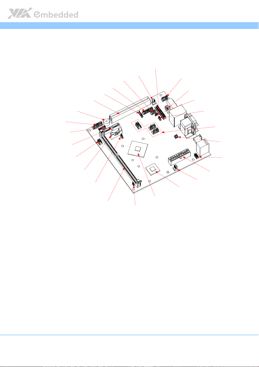
VIA C7-D processor
VIA VX900 chipset
SATA DOM voltage select jumper
Front panel pin header
SATA connectors
Front Audio pin header
SPDIF connector
COM voltage select jumper
Temperature sensor pin header
USB pin headers
JTV pin header
KB & MS pin header
ATX power connector
CPU fan connector
SMBus pin header
DDR3 DIMM slot
Clear CMOS jumper
CMOS battery
SPI pin header
Buzzer
PCI slot
SIR pin header
LPC pin header
COM pin header
System fan connector
LPT pin header
VB7008 User Manual
VB7008VB7008
1.3. Layout Diagram
User Manual
User ManualUser Manual
Figure
Figure 1111: Layout diagram of the
Figure Figure
6
: Layout diagram of the VB7008
: Layout diagram of the : Layout diagram of the
VB7008 mainboard
VB7008VB7008
mainboard (top view)
mainboard mainboard
(top view)
(top view) (top view)
Page 20

VB7008
VB7008 User Manual
VB7008VB7008
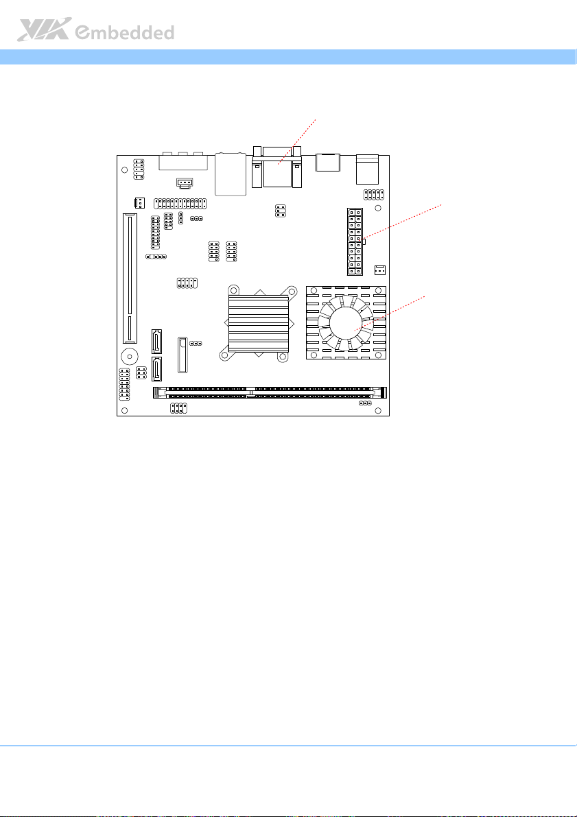
1.4. Product Dimensions
170.00 mm
10.16 mm
33.02
mm
170.00 mm
4.97 mm
6.17 mm
Figure
Figure 2222: Mounting holes and dimensions of the
: Mounting holes and dimensions of the VB7008
Figure Figure
: Mounting holes and dimensions of the : Mounting holes and dimensions of the
VB7008 mainboard
VB7008VB7008
6.35 mm
mainboard
mainboard mainboard
User Manual
User ManualUser Manual
Figure
Figure 3333:
Figure Figure
26.88 mm
23.35 mm
7.88 mm
8.10 mm
4.69 mm
: Exte
External
: :
ExteExte
158.75 mm
0.00
0.00
12.01 mm
35.79 mm
rnal I/O
I/O port
port dimensions of the VB7008 mainboard
rnal rnal
dimensions of the VB7008 mainboard
I/O I/O
portport
dimensions of the VB7008 mainboard dimensions of the VB7008 mainboard
67.95 mm
94.17 mm
122.66 mm
110.16 mm
2.54 mm
2.54 mm
44.45 mm
8.10 mm
135.16 mm
7
Page 21
VB7008
VB7008 User Manual
VB7008VB7008
1.5. Height Distribution
Height: 32.00 mm
Height: 33.00 mm
Height: 34.80 mm
User Manual
User ManualUser Manual
Figure
Figure 4444: Height distribution of the
: Height distribution of the VB7008
Figure Figure
: Height distribution of the : Height distribution of the
VB7008 mainboard
mainboard
VB7008VB7008
mainboard mainboard
8
Page 22
VB7008
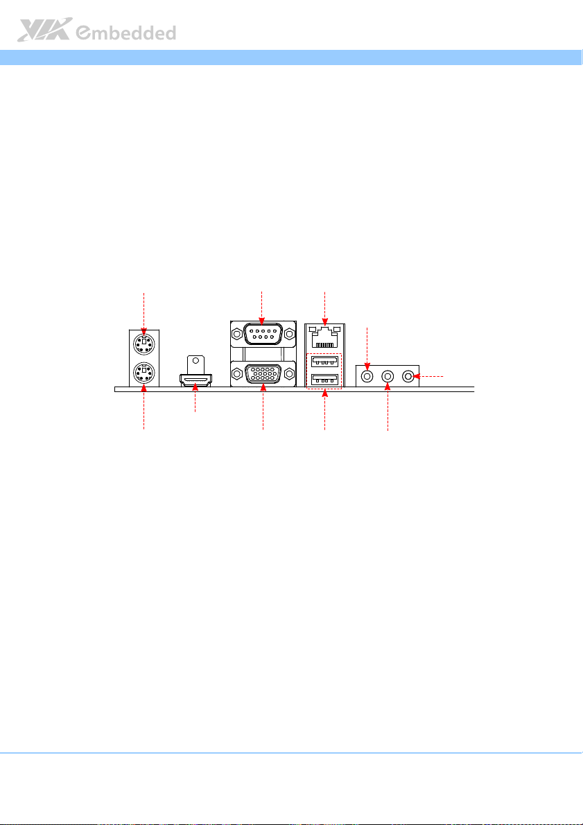
HDMI port
PS2 Mouse port
PS2 Keyboard port
VGA port
COM port GigaLAN port
USB ports
Line-Out
Line-In
MIC-In
2.
2. I/O Interface
I/O Interface
2.2.
I/O InterfaceI/O Interface
The VIA VB7008 has a wide selection of interfaces integrated into the board. It
includes a selection of frequently used ports as part of the external I/O
coastline.
VB7008 User Manual
VB7008VB7008
User Manual
User ManualUser Manual
2.1. External I/O Ports
Figure
Figure 5555: External I/O ports
: External I/O ports
Figure Figure
: External I/O ports: External I/O ports
9
Page 23
VB7008
VB7008 User Manual
VB7008VB7008
User Manual
User ManualUser Manual
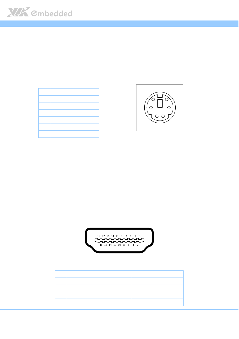
2.1.1. PS/2 Port
The mainboard has two integrated PS/2 ports for keyboard and mouse. Each
port is using the 6-pin Mini-DIN connector. The color purple is use for a PS/2
keyboard while the color green is use for a PS/2 mouse. The pinout of the PS/2
port are shown below.
Pin
Pin
Signal
Signal
PinPin
SignalSignal
5
1 Data
2 NC
3 Ground
4 +5V
5 Clock
6 NC
Table
Table 1111: PS/2 port pinout
: PS/2 port pinout
Table Table
: PS/2 port pinout: PS/2 port pinout
Figure
Figure 6666:
Figure Figure
6
34
12
: PS/2
PS/2 port pinout diagram
port pinout diagram
: :
PS/2PS/2
port pinout diagram port pinout diagram
2.1.2. HDMI
®
Port
The integrated 19-pin HDMI® port uses an HDMI® Type A receptacle
connector. The HDMI
®
(High Definition Multimedia Interface) port is for
connecting the high definition video and digital audio. It allows you to
connect the digital video devices which utilize a high definition video signal.
®
The pinout of the HDMI
port is shown below.
Figure
Figure 7777: HDMI
Figure Figure
®®®®
: HDMI
port pinout diagram
port pinout diagram
: HDMI: HDMI
port pinout diagram port pinout diagram
Pin
Pin
PinPin
1 TX2+ 2 Ground
3 TX2- 4 TX1+
5 Ground 6 TX1-
7 TX0+ 8 Ground
Signal
Signal Pin
SignalSignal
Pin
PinPin
Signa
Signallll
SignaSigna
10
Page 24

VB7008
9 TX0- 10 TXC+
11 Ground 12 TXC-
13 key 14 key
15 DDCSCL 16 DDCSDA
17 Ground 18 +5V
19 Hot Plug Detect
: HDMI
: HDMI: HDMI
®®®®
port pinout
port pinout
port pinout port pinout
Table
Table 2222: HDMI
Table Table
VB7008 User Manual
VB7008VB7008
User Manual
User ManualUser Manual
11
Page 25
VB7008
VB7008 User Manual
VB7008VB7008
User Manual
User ManualUser Manual
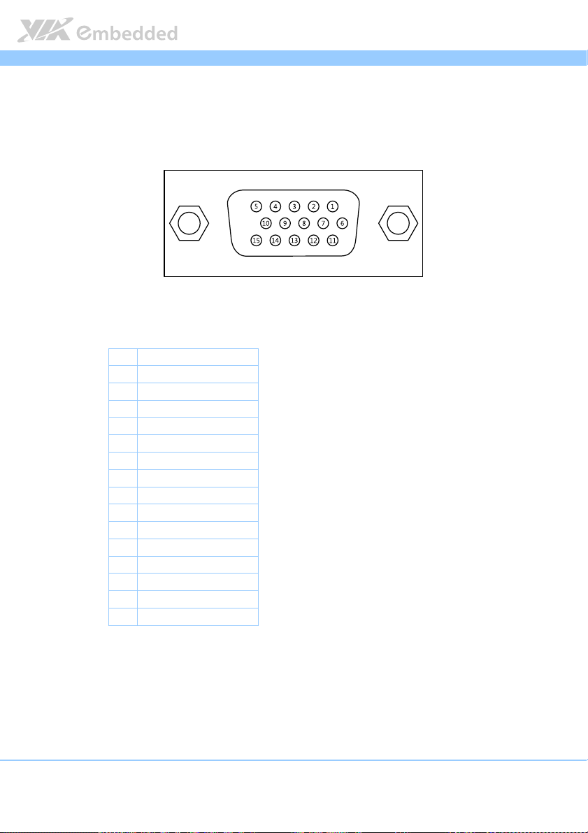
2.1.3. VGA Port
The integrated 15-pin VGA port uses a female DE-15 connector. The VGA
port is for connecting to analog displays. The pinout of the VGA port is shown
below.
Figure
Figure 8888: VGA port pinout diagram
: VGA port pinout diagram
Figure Figure
: VGA port pinout diagram: VGA port pinout diagram
Pin
Pin
Signal
Signal
PinPin
SignalSignal
1 RED
2 GREEN
3 BLUE
4 NC
5 Ground
6 Ground
7 Ground
8 Ground
9 +5V
10 NC
11 NC
12 SDA
13 HSync
14 VSync
15 SCL
Table
Table 3333: VGA port pinout
: VGA port pinout
Table Table
: VGA port pinout: VGA port pinout
12
Page 26
VB7008
VB7008 User Manual
VB7008VB7008
User Manual
User ManualUser Manual
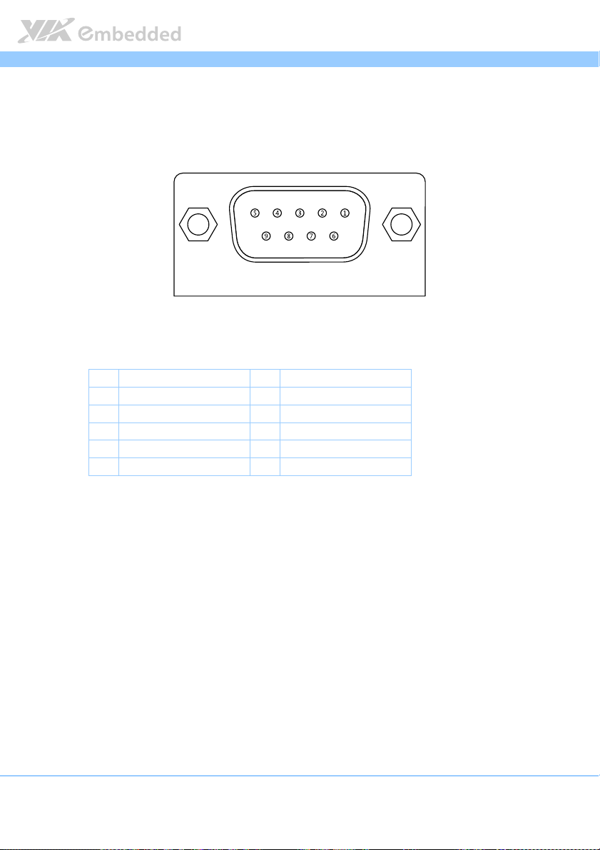
2.1.4. COM Port
The integrated 9-pin COM port uses a male DE-9 connector. The COM
(COM1) port supports the RS-232 standard. The pinout of the COM port is
shown below.
Figure
Figure 9999: COM port pinout diagram
: COM port pinout diagram
Figure Figure
: COM port pinout diagram: COM port pinout diagram
Pin
Pin
Signal
Signal Pin
PinPin
SignalSignal
1 DCD 6 DSR
2 RxD 7 RTS
3 TxD 8 CTS
4 DTR 9 RI
5 GND
Table
Table 4444:
: COM port pinout
Table Table
COM port pinout
: :
COM port pinoutCOM port pinout
Pin
PinPin
Signal
Signal
SignalSignal
13
Page 27
VB7008
VB7008 User Manual
VB7008VB7008
User Manual
User ManualUser Manual
2.1.5. USB 2.0 Port
There are two integrated USB 2.0 ports in VB7008 mainboard. The USB-
interface port gives complete Plug and Play and hot swap capability for
external devices and it complies with USB UHCI, rev. 2.0. Each USB port is
using the USB Type A receptacle connector. The pinout of the typical USB
port is shown below.
Pin
Pin
Signal
Signal
PinPin
SignalSignal
1 +5VSUS
2 Data-
3 Data+
4 Ground
Table
Table 5555: USB port pinout
: USB port pinout
Table Table
: USB port pinout: USB port pinout
Figure
Figure 10
10: USB port pinout diagram
Figure Figure
: USB port pinout diagram
1010
: USB port pinout diagram: USB port pinout diagram
14
Page 28
VB7008
VB7008 User Manual
VB7008VB7008
User Manual
User ManualUser Manual
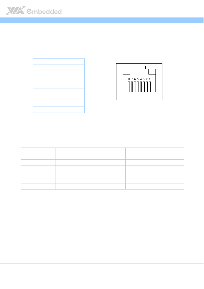
2.1.6. RJ45 LAN port: Gigabit Ethernet
The integrated 8-pin Gigabit Ethernet port is using an 8 Position 8 Contact
(8P8C) receptacle connector (commonly referred to as RJ45). The pinout of
the Gigabit Ethernet port is shown below.
Pin
Pin
Signal
Signal
PinPin
SignalSignal
1 Signal pair 1+
2 Signal pair 1-
3 Signal pair 2+
4 Signal pair 3+
5 Signal pair 3-
6 Signal pair 2-
7 Signal pair 4+
8 Signal pair 4-
Table
Table 6666: Gigabit Ethernet port pinout
: Gigabit Ethernet port pinout
Table Table
: Gigabit Ethernet port pinout: Gigabit Ethernet port pinout
Figure
Figure 11
11: Gigabit Ethernet port pinout diagram
Figure Figure
The RJ-45 port has two individual LED indicators located on the front side to
show its Active/Link status and Speed status.
: Gigabit Ethernet port pinout diagram
1111
: Gigabit Ethernet port pinout diagram: Gigabit Ethernet port pinout diagram
Link LED
(Left LED on RJ
(Left LED on RJ----45 connector)
(Left LED on RJ(Left LED on RJ
Link Off Off Off
Speed_10Mbit The LED is always On in either Green
or Orange colors
Speed_100Mbit The LED is always On in Green color Flash in Yellow color
Speed_1000Mbit The LED is always On in Orange color Flash in Yellow color
Table
Table 7777: Gigabit Ethernet LED color de
: Gigabit Ethernet LED color definition
Table Table
: Gigabit Ethernet LED color de: Gigabit Ethernet LED color de
Link LED
Link LEDLink LED
45 connector)
45 connector)45 connector)
finition
finitionfinition
Active LED
Active LED
Active LEDActive LED
(Right LED on RJ
(Right LED on RJ----45 connector)
(Right LED on RJ(Right LED on RJ
Flash in Yellow color
45 connector)
45 connector)45 connector)
15
Page 29
VB7008
VB7008 User Manual
VB7008VB7008
User Manual
User ManualUser Manual
2.1.7. Audio Ports
There are three audio jack receptacles integrated into a single stack on the I/O
coastline. Each receptacle can fit a 3.5 mm Tip Ring Sleeve (TRS) connector to
enable connections to Line-Out Line-In, and MIC-in. The Line-Out jack is for
connecting to external speakers or headphones. The Line-In jack is for
connecting an external audio devices such as CD player, tape player and etc..
The MIC-In jack is for connecting to a microphone.
Wiring
Wiring
WiringWiring
Tip Left channel Left channel in Left channel
Ring Right channel Right channel in Right channel
Sleeve Ground Ground Ground
Table
Table 8888: Audio jack receptacle pinout
Table Table
Line
Line----Out
Out Line
LineLine
OutOut
: Audio jack receptacle pinout
: Audio jack receptacle pinout: Audio jack receptacle pinout
Line----In
In MIC
LineLine
InIn
MIC----In
MICMIC
Line-Out
In
InIn
Figure
Figure 12
Figure Figure
Line-In
12: Audio jack receptacle stack
: Audio jack receptacle stack
1212
: Audio jack receptacle stack: Audio jack receptacle stack
MIC-In
16
Page 30
VB7008
VB7008 User Manual
VB7008VB7008
User Manual
User ManualUser Manual
2.2. Onboard Connectors
2.2.1. ATX Power Connector
The mainboard has a 20-pin ATX power connector onboard. The ATX power
connector is labeled as “ATX_POWER1”. The pinout of the ATX power
connector is shown below.
20
10
11
1
Figure
Figure 13
13: ATX power connector
Figure Figure
Table
Table 9999: ATX power connector pinout
Table Table
17
: ATX power connector
1313
: ATX power connector: ATX power connector
Pin
Pin
Signal
Signal Pin
PinPin
SignalSignal
1 +3.3V 11 +3.3V
2 +3.3V 12 -12V
3 Ground 13 Ground
4 +5V 14 Power Supply On
5 Ground 15 Ground
6 +5V 16 Ground
7 Ground 17 Ground
8 Power OK 18 -5V
9 +5VSB 19 +5V
10 +12V 20 +5V
: ATX power connector pinout
: ATX power connector pinout: ATX power connector pinout
Pin
PinPin
SSSSignal
ignal
ignalignal
Page 31

VB7008
VB7008 User Manual
VB7008VB7008
User Manual
User ManualUser Manual
2.2.2. CMOS Battery Slot
The mainboard is equipped with a CMOS battery slot, which is compatible
with CR2032 coin batteries. The CMOS battery slot is labeled as “BAT2”.
When inserting a CR2032 coin battery, be sure that the positive side is facing
the locking clip.
-
+
Figure
Figure 14
14: CMOS battery slot
Figure Figure
: CMOS battery slot
1414
: CMOS battery slot: CMOS battery slot
Pin
Pin
Signal
Signal
PinPin
SignalSignal
1 Ground
2 +3V
3 Ground
Table
Table 10
10: CMOS battery slot pinout
: CMOS battery slot pinout
Table Table
1010
: CMOS battery slot pinout: CMOS battery slot pinout
18
Page 32

VB7008
VB7008 User Manual
VB7008VB7008
User Manual
User ManualUser Manual
2.2.3. Front Panel Pin Header
The front panel pin header consists of 15 pins in a 16-pin block. Pin 15 is
keyed. The front panel pin header is labeled as “F_PANEL1”. It provides access
to system LEDs, power, reset, system speaker and HDD LED. The pinout of the
front panel pin header is shown below.
2
16
15
ader
aderader
Figure
Figure 15
15: Front panel pin he
Figure Figure
: Front panel pin header
1515
: Front panel pin he: Front panel pin he
1
Pin
Pin
Signal
Signal Pin
PinPin
SignalSignal
1 +5VDUAL 2 +5V
3 +5VDUAL 4 SATA_LED
5 PWR_LED 6 PWR_BTN
7 +5V 8 Ground
9 NC 10 -RST_SW
11 NC 12 Ground
13 SPEAK 14 +5V
15 key 16 NC
Table
Table 11
11: Front panel pin header pinout
: Front panel pin header pinout
Table Table
1111
: Front panel pin header pinout: Front panel pin header pinout
19
Pin
PinPin
Signal
Signal
SignalSignal
Page 33

VB7008
VB7008 User Manual
VB7008VB7008
User Manual
User ManualUser Manual
2.2.4. SMBus Pin Header
The SMBus pin header consists of three pins that allow connecting the SMBus
devices. Devices communicate with a SMBus host and/or other SMBus devices
using the SMBus interface. It is labeled as “SMBUS”. The pinout of the SMBus
pin header is shown below.
Pin
Pin
Signal
Signal
PinPin
SignalSignal
1 SMBCK
2 SMBDT
3 Ground
Table
Table 12
12: SMBus pin header
: SMBus pin header
Table Table
1212
: SMBus pin header: SMBus pin header
Figure
Figure 16
16: SMBus pin header
Figure Figure
: SMBus pin header pinout
1616
: SMBus pin header: SMBus pin header
pinout
pinout pinout
1
2.2.5. CPU and System Fan Connectors
There are two fan connectors on board: one for the CPU and one for the
chassis. The fan connector for the CPU is labeled as “CPUFAN1” and the fan
connector for the system is labeled as “SYSFAN1”. The fans provide variable
fan speeds controlled by the BIOS. The pinout of the fan connectors is shown
below.
20
Page 34

VB7008
CPUFAN1
1
SYSFAN1
1
VB7008 User Manual
VB7008VB7008
CPU
CPU fan
fan (C
(CPUFAN1
fanfan
(C (C
Signal
Signal
SignalSignal
PUFAN1))))
PUFAN1PUFAN1
CPU CPU
Pin
Pin
PinPin
1 FANIN1
2 FANCTL
3 Ground
System fan
System fan (SYSFAN1
System fanSystem fan
Pin
Pin
PinPin
1 FANIN2
2 FANCTL
3 Ground
Table
Table 13
13: Fan connector pinouts
: Fan connector pinouts
Table Table
1313
: Fan connector pinouts: Fan connector pinouts
(SYSFAN1))))
(SYSFAN1 (SYSFAN1
Signal
Signal
SignalSignal
Figure
Figure 17
Figure Figure
17: Fan connectors
: Fan connectors
1717
: Fan connectors: Fan connectors
User Manual
User ManualUser Manual
21
Page 35

VB7008
SATA1
SATA2
VB7008 User Manual
VB7008VB7008
User Manual
User ManualUser Manual
2.2.6. SATA Connectors
The two SATA connectors on board can support up to 3 Gb/s transfer speeds.
The SATA connectors are labeled as “SATA1” and “SATA2”. The pinout of the
SATA connectors are shown below.
SATA1
SATA1
SATA1SATA1
Pin
Pin
Signal
Signal
PinPin
SignalSignal
1 Ground
2 STXP_1
3 STXN_1
4 Ground
5 SRXN_1
6 SRXP_1
7 Ground
SATA2
SATA2
SATA2SATA2
Pin
Pin
Signal
Signal
PinPin
SignalSignal
1 Ground
2 STXP_2
3 STXN_2
4 Ground
5 SRXN_2
6 SRXP_2
7 SATA2_+5V
Table
Table 14
14: SATA connector pinouts
: SATA connector pinouts
Table Table
1414
: SATA connector pinouts: SATA connector pinouts
Figure
Figure 18
18: SATA connectors
Figure Figure
: SATA connectors
1818
: SATA connectors: SATA connectors
Note:
Note:
Note:Note:
If the users want to use the SATA Disk-on-Module flash drive on the board, please use the SATA2 connector.
22
Page 36

VB7008
VB7008 User Manual
VB7008VB7008
User Manual
User ManualUser Manual
2.2.7. USB 2.0 Pin Headers
The mainboard has three USB 2.0 pin header blocks that support up to six USB
2.0 ports. The pin header blocks are labeled as “USB_2”, USB_3, and “USB_4”.
The pinout of the USB pin headers are shown below.
USB_4
1
2
10
USB_2
2
1
Figure
Figure 19
19: USB pin headers
Figure Figure
: USB pin headers
1919
: USB pin headers: USB pin headers
USB_
USB_2222
USB_USB_
Pin
Pin
Signal
Signal Pin
PinPin
SignalSignal
1 VUSB2 2 VUSB2
3 USBD_T3- 4 USB_T2-
5 USBD_T3+ 6 USB_T2+
7 Ground 8 Ground
9 Key 10 Ground
USB_
USB_3333
USB_USB_
Pin
Pin
Signa
Signallll Pin
PinPin
SignaSigna
1 VUSB4 2 VUSB4
3 USBD_T5- 4 USB_T4-
5 USBD_T5+ 6 USB_T4+
7 Ground 8 Ground
9 Key 10 Ground
10
Pin
PinPin
Pin
PinPin
USB_3
1
10
2
Signal
Signal
SignalSignal
Signal
Signal
SignalSignal
23
Page 37

VB7008
USB_
USB_4444
USB_USB_
Pin
Pin
Signal
Signal Pin
PinPin
SignalSignal
1 VUSB6 2 VUSB6
3 USBD_T6- 4 USB_T7-
5 USBD_T6+ 6 USB_T7+
7 Ground 8 Ground
9 Key 10 Ground
Table
Table 15
15:
: USB pin header pinouts
Table Table
USB pin header pinouts
1515
: :
USB pin header pinoutsUSB pin header pinouts
Pin
PinPin
Signal
Signal
SignalSignal
VB7008 User Manual
VB7008VB7008
User Manual
User ManualUser Manual
24
Page 38

VB7008
VB7008 User Manual
VB7008VB7008
User Manual
User ManualUser Manual
2.2.8. COM Pin Header
The mainboard include one onboard COM pin header in addition to the COM
port 1 on the external I/O. The onboard COM pin header labeled as “COM2”
is used to attach additional COM port that supports RS-232 standard. The
pinout of the COM2 pin header is shown below.
2
1
9
Figure
Figure 20
20: COM pin header
Figure Figure
: COM pin header
2020
: COM pin header: COM pin header
Pin Signal Pin Signal
1 COM_DCD 2 COM_RXD
3 COM_TXD 4 COM_DTR
5 Ground 6 COM_DSR
7 COM_RTS 8 COM_CTS
9 COM_RI 10 key
Table
Table 16
16: COM pin header pinout
: COM pin header pinout
Table Table
1616
: COM pin header pinout: COM pin header pinout
25
Page 39

VB7008
VB7008 User Manual
VB7008VB7008
User Manual
User ManualUser Manual
2.2.9. PS/2 Keyboard and Mouse Pin Header
The mainboard has a pin header for a PS/2 keyboard and mouse. The pin
header is labeled as “KBMS1”. The pinout of the pin header is shown below.
10
Figure
Figure 21
21: PS/2 keyboard and mouse pin header
Figure Figure
: PS/2 keyboard and mouse pin header
2121
: PS/2 keyboard and mouse pin header: PS/2 keyboard and mouse pin header
Pin
Pin
Signal
Signal Pin
PinPin
SignalSignal
1 +5VDUAL 2 Ground
3 KB_CLK 4 KB_DATA
5 EKBCLK 6 EKBDATA
7 MS_CLK 8 MS_DATA
9 EMSCLK 10 EMSDATA
Table
Table 17
17: PS/2 keyboard and mouse pin header pinout
: PS/2 keyboard and mouse pin header pinout
Table Table
1717
: PS/2 keyboard and mouse pin header pinout: PS/2 keyboard and mouse pin header pinout
Note:
Note:
Note:Note:
When the pin header is not in use, please short pin 3&5, pin 4&6, pin 7&9 and pin 8&10
Pin
PinPin
Signal
Signal
SignalSignal
26
Page 40

VB7008
VB7008 User Manual
VB7008VB7008
User Manual
User ManualUser Manual
2.2.10. Front Audio Pin Header
In addition to the TRS audio jacks on the external I/O coastline, the mainboard
has a pin header for Line-Out and MIC-In. The pin header is labeled as
“F_AUDIO1”. The pinout of the pin header is shown below.
Figure
Figure 22
22: Front audio pin header
Figure Figure
: Front audio pin header
2222
: Front audio pin header: Front audio pin header
Pin
Pin
Signal
Signal Pin
PinPin
SignalSignal
1 MIC2IN_L 2 AGND
3 MIC2IN_R 4 AGND
5 HPOUTR 6 MIC2_JD
7 F_AUDIO_SENSE 8 Key
9 HPOUTL 10 HPOUT_JD
Table
Table 18
18: Front audio pin header pinout
: Front audio pin header pinout
Table Table
1818
: Front audio pin header pinout: Front audio pin header pinout
27
Pin
PinPin
Signal
Signal
SignalSignal
Page 41

VB7008
VB7008 User Manual
VB7008VB7008
User Manual
User ManualUser Manual
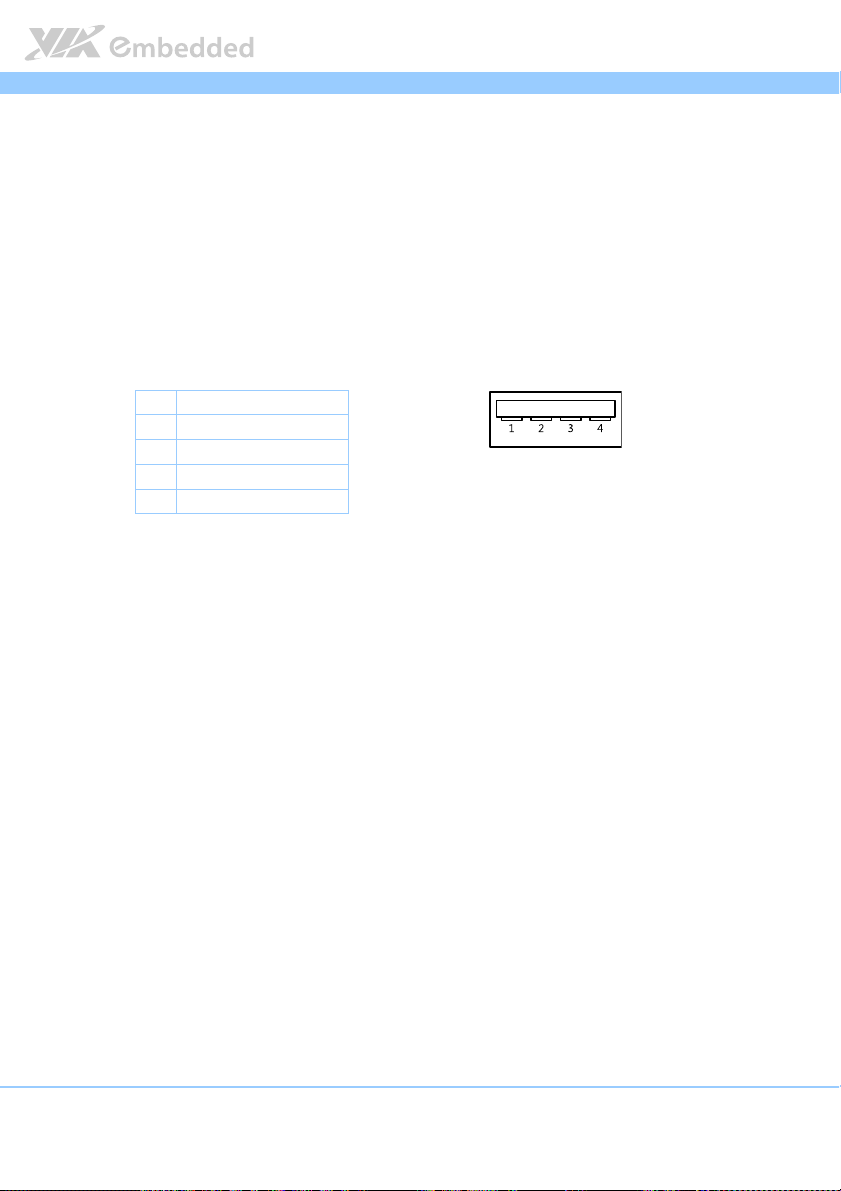
2.2.11. SPDIF Connector
The mainboard has one 3-pin SPDIF (Sony Philips Digital Interface) connector.
The SPDIF output provides digital audio to external speakers or compressed
AC3 data to an external Dolby Digital Decoder. The connector is labeled as
“SPDIF1”. The pinout of the connector is shown below.
1
Figure
Figure 23
23: SPDIF connector
Figure Figure
: SPDIF connector
2323
: SPDIF connector: SPDIF connector
Pin
Pin
Signal
Signal
PinPin
SignalSignal
1 VDD
2 SPDIFO
3 Ground
Table
Table 19
19: SPDIF connector pinout
: SPDIF connector pinout
Table Table
1919
: SPDIF connector pinout: SPDIF connector pinout
28
Page 42

VB7008
1
8
VB7008 User Manual
VB7008VB7008
User Manual
User ManualUser Manual
2.2.12. SPI Pin Header
The mainboard has one 8-pin SPI pin header. The SPI (Serial Peripheral
Interface) pin-header is used to connect to the SPI BIOS programming fixture.
The pin header is labeled as “SPI1”. The pinout of the pin header is shown
below.
Figure
Figure 24
24: SPI pin header
Figure Figure
: SPI pin header
2424
: SPI pin header: SPI pin header
Pin
Pin
Signal
Table
Table 20
20: SPI pin header pinout
: SPI pin header pinout
Table Table
2020
: SPI pin header pinout: SPI pin header pinout
Signal Pin
PinPin
SignalSignal
1 SPIVCC 2 Ground
3 MSPISS0 4 MSPICLK
5 MSPIDI 6 MSPIDO
7 key 8 -PCIRST
Pin
PinPin
Signal
Signal
SignalSignal
29
Page 43

VB7008
VB7008 User Manual
VB7008VB7008
User Manual
User ManualUser Manual
2.2.13. LPC Pin Header
The mainboard has one LPC pin header for connecting LPC devices. The pin
header is labeled as “LPC”. The pinout of the pin header is shown below.
2
1
19
Figure
Figure 25
25: LPC pin header
Figure Figure
: LPC pin header
2525
: LPC pin header: LPC pin header
Pin
Pin
Signal
Table
Table 21
21: LPC pin header pinout
: LPC pin header pinout
Table Table
2121
: LPC pin header pinout: LPC pin header pinout
Signal Pin
PinPin
SignalSignal
1 LAD1 2 LPCIF_33_CLK
3 -PCIRSTX 4 Ground
5 LAD0 6 LPCIF_48_CLK
7 LAD2 8 _LFRAME
9 SERIRQ 10 LAD3
11 -LDRQ1 12 -EXTSMI
13 +5V 14 +3.3V
15 +5V 16 +3.3V
17 Ground 18 Ground
19 Ground 20 NC
Pin
PinPin
Signal
Signal
SignalSignal
30
Page 44

VB7008
VB7008 User Manual
VB7008VB7008
User Manual
User ManualUser Manual
2.2.14. LPT Pin Header
The mainboard has one LPT pin header for connecting 25-pin LPT female
external connector for parallel port. A parallel port is a standard printer port
that supports Enhanced Parallel Port (EPP) and Extended Capabilities Parallel
Port (ECP) modes. The pin header is labeled as “LPT1”. The pinout of the pin
header is shown below.
1
25
Figure
Figure 26
26: LPT pin header
Figure Figure
31
: LPT pin header
2626
: LPT pin header: LPT pin header
Pin
Pin
Signal
Signal Pin
PinPin
SignalSignal
1 -LP_STB 2 -LP_AFD
3 LP_D0 4 -LP_ERR
5 LP_D1 6 -LP_INIT
7 LP_D2 8 -LP-SLIN
9 LP_D3 10 Ground
11 LP_D4 12 Ground
13 LP_D5 14 Ground
15 LP_D6 16 Ground
17 LP_D7 18 Ground
Pin
PinPin
Signal
Signal
SignalSignal
Page 45

VB7008
19 -LP_ACK 20 Ground
21 LP_BUSY 22 Ground
23 LP_PE 24 Ground
25 LP_SLCT 26 Key
Table
Table 22
22: LPT pin header pinout
: LPT pin header pinout
Table Table
2222
: LPT pin header pinout: LPT pin header pinout
VB7008 User Manual
VB7008VB7008
User Manual
User ManualUser Manual
32
Page 46

VB7008
VB7008 User Manual
VB7008VB7008
User Manual
User ManualUser Manual
2.2.15. SIR Pin Header
The mainboard has SIR (Serial Infrared) pin header. This pin header is used to
connect to a serial infrared module. The pin header is labeled as “SIR1”. The
pinout of the SIR pin header is shown below.
1
Figure
Figure 27
27: SIR pin header
Figure Figure
: SIR pin header
2727
: SIR pin header: SIR pin header
Pin
Pin
Signal
Signal
PinPin
SignalSignal
1 +5V
2 NC
3 IRRX
4 Ground
5 IRTX
Table
Table 23
23: S
: SIR pin header pinout
Table Table
IR pin header pinout
2323
: S: S
IR pin header pinoutIR pin header pinout
Note:
Note:
Note:Note:
Microsoft Windows Vista and Windows 7 do not support the Infrared driver.
33
Page 47

VB7008
VB7008 User Manual
VB7008VB7008
User Manual
User ManualUser Manual
2.2.16. Temperature Sensor Pin Header
The mainboard supports a pin header (3-pin) that allows the connection of a
temperature sensor cable for detecting the system’s internal air temperature.
The temperature reading can be seen in the BIOS Setup Utility. The pin header
is labeled as “J5”. The pin out of the temperature sensor pin header is shown
below.
1
Figure
Figure 28
28: Temperature sensor pin h
Figure Figure
: Temperature sensor pin header
2828
: Temperature sensor pin h: Temperature sensor pin h
eader
eadereader
Pin
Pin
Signal
Signal
PinPin
SignalSignal
1 TMPIN2
2 TMPIN2
3 HWMGND
Table
Table 24
24: Temperature sensor pin header pinout
: Temperature sensor pin header pinout
Table Table
2424
: Temperature sensor pin header pinout: Temperature sensor pin header pinout
34
Page 48

VB7008
1
2
5
☎
VB7008 User Manual
VB7008VB7008
User Manual
User ManualUser Manual
2.2.17.Composite + S-Video Out Pin Header (optional)
The mainboard provide an optional Composite + S-Video out pin header that
allows connecting the TV port/jack connector in order to interface TV monitor
or S-Video device to the mainboard. The pin header is labeled as “JTV1”. The
pinout of the pin header is shown below.
Figure
Figure 29
29: Composite + S
Figure Figure
: Composite + S----Video pin header
2929
: Composite + S: Composite + S
Table
Table 25
25: Composite + S
: Composite + S----Video pin header pinout
Table Table
2525
: Composite + S: Composite + S
Video pin header
Video pin headerVideo pin header
Pi
Pinnnn
Signal
Signal Pin
PiPi
SignalSignal
1 CVBS 2 Ground
3 CHROMA 4 key
5 LUMA 6 Ground
Video pin header pinout
Video pin header pinoutVideo pin header pinout
Pin
PinPin
Signal
Signal
SignalSignal
35
Page 49

Page 50

VB7008
3.
3. Jumpers
Jumpers
3.3.
JumpersJumpers
VB7008 User Manual
VB7008VB7008
User Manual
User ManualUser Manual
3.1. Clear CMOS Jumper
The onboard CMOS RAM stores system configuration data and has an onboard
battery power supply. To reset the CMOS settings, set the jumper on pins 2
and 3 while the system is off. Return the jumper to pins 1 and 2 afterwards.
Setting the jumper while the system is on will damage the mainboard. The
default setting is on pins 1 and 2.
1
Fig
Figure
ure 30
30: CLEAR CMOS jumper
FigFig
Table
Table 26
Table Table
: CLEAR CMOS jumper
ure ure
3030
: CLEAR CMOS jumper: CLEAR CMOS jumper
Setting
Setting Pin 1
SettingSetting
Regular (default) On On Off
Clear CMOS Off On On
26: CLEAR CMOS jumper settings
: CLEAR CMOS jumper settings
2626
: CLEAR CMOS jumper settings: CLEAR CMOS jumper settings
Pin 1 Pin 2
Pin 1Pin 1
Pin 2 Pin 3
Pin 2Pin 2
Pin 3
Pin 3Pin 3
37
Page 51

VB7008
VB7008 User Manual
VB7008VB7008
Note:
Note:
Note:Note:
Except when clearing the RTC RAM, never remove the cap from the CLEAR_CMOS jumper default
position. Removing the cap will cause system boot failure. Avoid clearing the CMOS while the system
is on; it will damage the mainboard.
User Manual
User ManualUser Manual
38
Page 52

VB7008
VB7008 User Manual
VB7008VB7008
User Manual
User ManualUser Manual
3.2. COM2 Voltage Select Jumper
The additional COM port (available through the onboard COM2 pin header,
see page 25) can support both +5V and +12V. The COM2 voltage select pin
jumper is a selector to determine the input voltage of COM2 pin header
connector. The voltage can be either +5V or +12V. +5V is the default setting.
The pin jumper is labeled as “J6”. The jumper settings are shown below.
1
Figure
Figure 31
31: COM
: COM2222 voltage select jumper
Figure Figure
3131
voltage select jumper
: COM: COM
voltage select jumper voltage select jumper
Setting
Table
Table 27
27: COM
Table Table
2727
Setting Pin 1
SettingSetting
+5V On On Off
+12V Off On On
: COM2222 voltage s
voltage select jumper settings
: COM: COM
voltage s voltage s
elect jumper settings
elect jumper settingselect jumper settings
Pin 1 Pin 2
Pin 1Pin 1
Pin 2 Pin 3
Pin 2Pin 2
Pin 3
Pin 3Pin 3
39
Page 53

VB7008
VB7008 User Manual
VB7008VB7008
User Manual
User ManualUser Manual
3.3. SATA DOM Voltage Select Jumper
The SATA2 connector (see page 22) can be used to support Disk-on-Module
th
(DOM) flash drive. When the jumper is set, +5V will be delivered to the 7
pin of the SATA2 connector. The pin jumper is labeled as “J2”. The jumper
settings are shown below.
2
6
1
5
Figure
Figure 32
32:
: SATA DOM voltage select jumper
Figure Figure
SATA DOM voltage select jumper
3232
: :
SATA DOM voltage select jumperSATA DOM voltage select jumper
SATA2 Setting
SATA2 Setting Pin 2
SATA2 SettingSATA2 Setting
DOM support On On Off
Regular (default) Off On On
Table
Table 28
28:
: SATA DOM voltage select jumper settings
Table Table
SATA DOM voltage select jumper settings
2828
: :
SATA DOM voltage select jumper settingsSATA DOM voltage select jumper settings
Note:
Note:
Note:Note:
The default settings of “SATA DOM Voltage Select Jumper”: short pin 3&5 and pin 4&6
Pin 2 Pin 4
Pin 2Pin 2
Pin 4 Pin 6
Pin 4Pin 4
Pin 6
Pin 6Pin 6
40
Page 54

VB7008
DIMM1
4.
4. Expansion Slots
Expansion Slots
4.4.
Expansion SlotsExpansion Slots
VB7008 User Manual
VB7008VB7008
User Manual
User ManualUser Manual
4.1. DDR3 Memory Slots
The mainboard provide one DDR3 DIMM memory slot. The memory slot can
accommodate up to 4 GB of 1066 MHz memory. The memory slot is labeled
as “DIMM1”. The location of the DDR3 memory slot is shown below.
Figure
Figure 33
33: DDR3 memory slot
Figure Figure
41
: DDR3 memory slotssss
3333
: DDR3 memory slot: DDR3 memory slot
Page 55

VB7008
VB7008 User Manual
VB7008VB7008
User Manual
User ManualUser Manual
4.1.1. Installing a Memory Module
Step 1
Step 1
Step 1Step 1
Disengage the locking mechanism at both ends of the DIMM slot by pressing
the retaining clips outward.
Figure
Figure 34
34: Unlocking the memory DIMM slot
Figure Figure
Step
Step 2222
Step Step
Align the notch on the DIMM memory module with the counter part on the
DIMM slot.
: Unlocking the memory DIMM slot
3434
: Unlocking the memory DIMM slot: Unlocking the memory DIMM slot
Figure
Figure 35
35: I
: Inserting the
Figure Figure
nserting the memory
3535
: I: I
nserting thenserting the
memory module
memory memory
module
modulemodule
42
Page 56

VB7008
Step
Step 3333
Step Step
VB7008 User Manual
VB7008VB7008
User Manual
User ManualUser Manual
Insert the DIMM memory module into the slot and push down at both ends
until the locking clips lock the DIMM memory module into place.
Figure
Figure 36
36:
: Locking the memory module
Figure Figure
Locking the memory module
3636
: :
Locking the memory moduleLocking the memory module
43
Page 57

VB7008
VB7008 User Manual
VB7008VB7008
User Manual
User ManualUser Manual
4.1.2. Removing a Memory Module
Step 1
Step 1
Step 1Step 1
To disengage the locking clips, push outward the locking clips on both ends
of memory slot. When the locking clips have cleared, the DIMM memory
module will automatically pop up. Remove the memory module.
Figure
Figure 37
37:
: Removing the memory module
Figure Figure
Removing the memory module
3737
: :
Removing the memory moduleRemoving the memory module
44
Page 58

VB7008
VB7008 User Manual
VB7008VB7008
User Manual
User ManualUser Manual
4.1.3. PCI Slot
The onboard PCI slot, labeled as “PCI_SLOT1”, supports 5V 32-bit PCI cards. It
is not compatible with PCI cards requiring 3.3V signaling. The location of the
PCI slot is shown below.
key notch
Figure
Figure 38
38: PCI slot
Figure Figure
: PCI slot
3838
: PCI slot: PCI slot
Note:
1. The orientation of PCI card can be changed from vertical to horizontal using a riser card module.
2. When adding or removing expansion card, unplug first the power supply.
45
Page 59

Page 60

VB7008
10.00 mm
5.00 mm
10.00 mm
100.00 mm
1.00 mm
5.
5. Hardware Installation
Hardware Installation
5.5.
Hardware InstallationHardware Installation
VB7008 User Manual
VB7008VB7008
User Manual
User ManualUser Manual
5.1. Installing into a Chassis
The VB7008 can be fitted into any chassis that has the mounting holes for
compatible with the standard Mini-ITX mounting hole locations. Additionally,
the chassis must meet the minimum height requirements for specified areas of
the mainboard. If a riser card module is being used, the chassis will need to
accommodate the additional space requirements.
5.1.1. Suggested minimum chassis dimensions
The figure below shows the suggested minimum space requirements that a
chassis should have in order to work well with the VB7008.
Figure
Figure 39
39: Suggested minimum chassis dimensions
Figure Figure
Each side of the mainboard should have a buffer zone from the internal wall
of the chassis. The side of the mainboard that accommodates the I/O coastline
should have a buffer of 1.00 mm. The side on the opposite end of the I/O
: Suggested minimum chassis dimensions
3939
: Suggested minimum chassis dimensions: Suggested minimum chassis dimensions
47
Page 61

VB7008
100.00 mm
(70.00 mm if
using riser card)
45.00 mm
50.00 mm
47.00 mm
56.00 mm
VB7008 User Manual
VB7008VB7008
User Manual
User ManualUser Manual
coastline should have a buffer of at least 5.00 mm. The two sides adjacent to
the I/O coastline should have at least a 10.00 mm buffer.
For the side that is close to the PCI slot, the buffer should be at least 100.00
mm if a riser card module will be used.
5.1.2. Suggested minimum chassis height
The figure below shows the suggested minimum height requirements for the
internal space of the chassis. It is not necessary for the internal ceiling to be
evenly flat. What is required is that the internal ceiling height must be strictly
observed for each section that is highlighted. The highest part of the ceiling
will be above the PCI slot.
Figure
Figure 40
40: Suggested minimum internal chassis c
Figure Figure
: Suggested minimum internal chassis ceiling height
4040
: Suggested minimum internal chassis c: Suggested minimum internal chassis c
48
eiling height
eiling heighteiling height
Page 62

VB7008
VB7008 User Manual
VB7008VB7008
User Manual
User ManualUser Manual
5.1.3. Suggested keepout areas
The figure below shows the areas of the mainboard that is highly suggested to
leave unobstructed.
Keep out area
Figure
Figure 41
41: Suggested keepout areas
Figure Figure
: Suggested keepout areas
4141
: Suggested keepout areas: Suggested keepout areas
49
Page 63

VB7008
VB7008 User Manual
VB7008VB7008
User Manual
User ManualUser Manual
50
Page 64

VB7008
6.
6. BIOS Setup Utility
BIOS Setup Utility
6.6.
BIOS Setup UtilityBIOS Setup Utility
VB7008 User Manual
VB7008VB7008
6.1. Entering the BIOS Setup Utility
User Manual
User ManualUser Manual
Power on the computer and press Delete
sequence to enter the BIOS Setup Utility. If the entry point has passed, restart
the system and try again.
Delete during the beginning of the boot
DeleteDelete
6.2. Control Keys
Up
Up Move up one row
UpUp
Down
Down Move down one row
DownDown
Left
Left Move to the left in the navigation bar
LeftLeft
Right
Right Move to the right in the navigation bar
RightRight
Enter
Enter Access the highlighted item / Select the item
EnterEnter
Esc
Esc Jumps to the Exit screen or returns to the previous screen
EscEsc
Page up /
Page up / ++++1 Increase the numeric value
Page up / Page up /
1
Page down /
Page down / ----
Page down / Page down /
F1
F1 General help
F1F1
FFFF5555 Restore the previous CMOS value
FFFF7777 Load optimized defaults
Decrease the numeric value
2
F10
F10 Save all the changes and exit
F10F10
Note:
Note:
Note:Note:
1. Must be pressed using the 10-key pad.
2. The General help contents are only for the Status Page and Option Page setup menus.
51
Page 65

VB7008
VB7008 User Manual
VB7008VB7008
6.3. Navigating the BIOS Menus
User Manual
User ManualUser Manual
The main menu displays all the BIOS setup categories. Use the <Left
and <Up
Up>/<Down
Down> arrow keys to select any item or sub-menu. Descriptions
UpUp
DownDown
of the selected/highlighted category are displayed at the bottom of the screen.
The small triangular arrowhead symbol next to a field indicates that a sub-
menu is available (see figure below). Press <Enter
To exit the sub-menu, press <Esc
Esc>.
EscEsc
Enter> to display the sub-menu.
EnterEnter
Left>/<Right
LeftLeft
Right>
RightRight
6.4. Getting Help
The BIOS Setup Utility provides a “General Help
accessed at any time by pressing F1
using and navigating the BIOS Setup Utility. Press Esc
General Help” screen. This screen can be
General HelpGeneral Help
F1. The help screen displays the keys for
F1F1
Esc to exit the help screen.
EscEsc
52
Page 66

VB7008
Phoenix - AwardBIOS CMOS Setup Utility
Standard CMOS Features
Advanced BIOS Features
Advanced Chipset Features
Integrated Peripherals
Power Management Setup
PnP/PCI Configurations
PC Health Status
Frequency/Voltage Control
Load Optimized Defaults
Set Supervisor Password
Set User Password
Save & Exit Setup
Exit Without Saving
Time, Date, Hard Disk Type...
Esc: Quit
F10: Save & Exit Setup
: Select Item
VB7008 User Manual
VB7008VB7008
User Manual
User ManualUser Manual
6.5. Main Menu
The Main Menu contains thirteen setup functions and two exit choices. Use
arrow keys to select the items and press <Enter
Figure
Figure 42
42: Illustration of the Main menu screen
Figure Figure
: Illustration of the Main menu screen
4242
: Illustration of the Main menu screen: Illustration of the Main menu screen
6.5.1. Standard CMOS Features
Use this menu to set basic system configurations.
Enter> to accept or enter Sub-menu.
EnterEnter
6.5.2. Advanced BIOS Features
Use this menu to set the advanced features available on your system.
6.5.3. Advanced Chipset Features
Use this menu to set chipset specific features and optimize system
performance.
6.5.4. Integrated Peripherals
Use this menu to set onboard peripherals features.
6.5.5. Power Management Setup
53
Page 67

VB7008
Use this menu to set onboard power management functions.
VB7008 User Manual
VB7008VB7008
User Manual
User ManualUser Manual
6.5.6. PnP/PCI Configurations
Use this menu to set the PnP and PCI configurations.
6.5.7. PC Health Status
This menu shows the PC health status.
6.5.8. Frequency/Voltage Control
Use this menu to set the system frequency and voltage control.
6.5.9. Load Optimized Defaults
Use this menu option to load BIOS default settings for optimal and high
performance system operations.
6.5.10. Set Supervisor Password
Use this menu option to set the BIOS supervisor password.
6.5.11. Set User Password
Use this menu option to set the BIOS user password.
6.5.12. Save & Exit Setup
Save BIOS setting changes and exit setup.
6.5.13. Exit Without Saving
Discard all BIOS setting changes and exit setup
54
Page 68

VB7008
VB7008 User Manual
VB7008VB7008
6.6. Standard CMOS Features
Phoenix - AwardBIOS CMOS Setup Utility
Standard CMOS Features
Date (mm:dd:yy)
Time (hh:mm:ss) 3 : 17 : 8
IDE Channel 0 Master
IDE Channel 0 Slave
Halt On [All, But Keyboard]
Base Memory
Extended Memory
Total Memory
Enter: Select +/-/PU/PD: Value
: Move
F5: Previous Values
Mon, Aug 15 2011
[None]
[None]
640K
784384K
785408K
6.6.1. Date
The date format is [Day, Month Date, Year]
6.6.2. Time
The time format is [Hour : Minute : Second]
F10: Save
F7: Optimized Defaults
Item Help
Menu Level
Change the day, month, year
and century
ESC: Exit
F1: General Help
User Manual
User ManualUser Manual
6.6.3. Halt On
Set the system’s response to specific boot errors. Below is a table that details
the possible settings.
Settings
Settings Description
SettingsSettings
All Errors System halts when any error is detected
No Errors System does not halt for any error
All, But Keyboard System halts for all non-key errors
55
Description
DescriptionDescription
Page 69

VB7008
IDE HDD Auto-Detection
IDE Channel 0 Master
Access Mode
Capacity
Cylinder
Precomp
Landing Zone
To auto-detect the HDD's
size, head... on this
channel
IDE Channel 0 Master
[Press Enter]
[Auto]
[Auto]
0 MB
0
Head 0
Sector
0
0
0
Phoenix - AwardBIOS CMOS Setup Utility
Item Help
Menu Level
ESC: Exit
F5: Previous Values
: Move
F10: Save
Enter: Select +/-/PU/PD: Value
F1: General Help
F7: Optimized Defaults
VB7008 User Manual
VB7008VB7008
6.7. IDE Channels
Channel 0 Master
Channel 0 Master
Channel 0 MasterChannel 0 Master
Channel 0
Channel 0 Slave
Channel 0 Channel 0
Slave
SlaveSlave
User Manual
User ManualUser Manual
Phoenix - AwardBIOS CMOS Setup Utility
IDE Channel 0 Slave
IDE HDD Auto-Detection
IDE Channel 0 Slave
Access Mode
Capacity
Cylinder
Head 0
Precomp
Landing Zone
56
Sector
: Move
Enter: Select +/-/PU/PD: Value
F5: Previous Values
[Press Enter]
[Auto]
[Auto]
0 MB
0
0
0
0
F10: Save
F7: Optimized Defaults
Item Help
Menu Level
To auto-detect the HDD's
size, head... on this
channel
ESC: Exit
F1: General Help
Page 70

VB7008
VB7008 User Manual
VB7008VB7008
User Manual
User ManualUser Manual
The specifications of your drive must match with the drive table. The hard disk
will not work properly if you enter incorrect information in this category.
Select “Auto”
“Auto” whenever possible. If you select “Manual”
“Auto”“Auto”
“Manual”, make sure the
“Manual”“Manual”
information is from your hard disk vendor or system manufacturer.
Below is a table that details required hard drive information when using the
““““Manual”
Manual” mode.
Manual”Manual”
Settings
Settings Description
SettingsSettings
[storage] Channel The name of this match the name of the menu.
Access Mode Settings: [CHS, LBA, Large, Auto]
Capacity Formatted size of the storage device
Cylinder Number of cylinders
Head Number of heads
Precomp Write precompensation
Landing Zone Cylinder location of the landing zone
Sector Number of sectors
Description
DescriptionDescription
Settings: [None, Auto, Manual]
57
Page 71

VB7008
Hard Disk Boot Priority
Quick Power On Self Test
Second Boot Device
Boot Other Device
Advanced BIOS Features
[Press Enter]
[Enabled]
First Boot Device [None]
[None]
[On]
Boot Up NumLock Status [Disabled]
Security Option [Setup]
Third Boot Device [None]
Full Screen LOGO Show [Disabled]
Summary Screen Show [Disabled]
Select Hard Disk Boot
Device Priorityl
Phoenix - AwardBIOS CMOS Setup Utility
Item Help
Menu Level
ESC: Exit
F5: Previous Values
: Move
F10: Save
Enter: Select +/-/PU/PD: Value
F1: General Help
F7: Optimized Defaults
VB7008 User Manual
VB7008VB7008
User Manual
User ManualUser Manual
6.8. Advanced BIOS Features
The Advanced BIOS Features section includes the following submenus:
Hard Disk Boot Priority
6.8.1. Quick Power On Self-Test
Shortens Power On Self-Test (POST) cycle to enable shorter boot up time.
Settings
Settings Description
SettingsSettings
Description
DescriptionDescription
Disabled Standard Power On Self Test (POST)
Enabled Shorten Power On Self Test (POST) cycle and boot up time
6.8.2. First/Second/Third Boot Device
Set the boot device sequence as BIOS attempts to load the disk operating
system.
Settings
Settings Description
SettingsSettings
Removable Boot from external drive
Hard Disk Boot from the HDD
CDROM Boot from CDROM
Legacy LAN Boot from network drive
VIA Networking Boot from network drive
Disabled Disable the boot device sequence
58
Description
DescriptionDescription
Page 72

VB7008
VB7008 User Manual
VB7008VB7008
User Manual
User ManualUser Manual
6.8.3. Boot Other Device
Enables the system to boot from alternate devices if the system fails to boot
from the “First/Second/Third Boot Device” lists.
Settings
Settings Description
SettingsSettings
Disabled No alternate boot device allowed
Enabled Enable alternate boot device
Description
DescriptionDescription
6.8.4. Boot Up NumLock Status
Set the NumLock status when the system is powered on.
Settings
Settings Description
SettingsSettings
Off Forces keypad to behave as arrow keys
On Forces keypad to behave as 10-key
Description
DescriptionDescription
6.8.5. Security Option
Selects whether the password is required every time the System boots, or only
when you enter Setup.
Settings
Settings Description
SettingsSettings
Setup Password prompt appears only when end users try to run BIOS
System Password prompt appears every time when the computer is powered
Description
DescriptionDescription
Setup
on and when end users try to run BIOS Setup
6.8.6. Full Screen Logo Show
Show full screen logo during BIOS boot up process.
Settings: [Disabled, Enabled]
6.8.7. Summary Screen Show
Show summary screen.
Settings: [Disabled, Enabled]
59
Page 73

VB7008
1. Bootable Add-in Cards
Hard Disk Boot Priority
Use < > or < > to
select a device, then
press < + > to move it
up, or < - > to move it
down the list. Press
<ESC> to exit this
menu.
Phoenix - AwardBIOS CMOS Setup Utility
Item Help
Menu Level
ESC: Exit
F5: Previous Values
: Move
F10: Save
Enter: Select +/-/PU/PD: Value
F1: General Help
F7: Optimized Defaults
VB7008 User Manual
VB7008VB7008
User Manual
User ManualUser Manual
6.9. Hard Disk Boot Priority
This is for setting the priority of the hard disk boot order when the “Hard Disk”
option is selected in the “[First/Second/Third] Boot Device” menu item.
60
Page 74

VB7008
Advanced Chipset Features
[Press Enter]
UMA & P2P Bridge Control
[Press Enter]
CPU & PCI Bus Control
[Press Enter]PCIE Bus Control
Phoenix - AwardBIOS CMOS Setup Utility
Item Help
Menu Level
ESC: Exit
F5: Previous Values
: Move
F10: Save
Enter: Select +/-/PU/PD: Value
F1: General Help
F7: Optimized Defaults
VB7008 User Manual
VB7008VB7008
User Manual
User ManualUser Manual
6.10. Advanced Chipset Features
Caution:
Caution:
Caution: Caution:
The Advanced Chipset Features menu is used for optimizing the chipset functions. Do not change
these settings unless you are familiar with the chipset.
The Advanced Chipset Features section includes the following submenus:
PCIE Bus Control
UMA & P2P Bridge Control
CPU & PCI Bus Control
61
Page 75

VB7008
PCIE Root Port
PCIE Target Link Speed
PCIE Bus Control
[Enable]
[Auto]
Phoenix - AwardBIOS CMOS Setup Utility
Item Help
Menu Level
ESC: Exit
F5: Previous Values
: Move
F10: Save
Enter: Select +/-/PU/PD: Value
F1: General Help
F7: Optimized Defaults
VB7008 User Manual
VB7008VB7008
6.11. PCIE Bus Control
6.11.1. PCIE Root Port
Settings: [Disabled, Enabled]
6.11.2. PCIE Target Link Speed
Settings: [Auto, Force Gen1]
User Manual
User ManualUser Manual
62
Page 76

VB7008
UMA Enable
VGA Share Memory Size
Select Display Device
Select Display Device 2
UMA & P2P Bridge Control
[Enable]
[256M]
CPU Direct Access FB [Enable]
[Manual]
[HDMI]
Select Display Device 1 [CRT]
TV_Type [NTSC]
TV_Connector: Composite [Enabled]
TV_Connector: S-Video [Enabled]
Phoenix - AwardBIOS CMOS Setup Utility
Item Help
Menu Level
ESC: Exit
F5: Previous Values
: Move
F10: Save
Enter: Select +/-/PU/PD: Value
F1: General Help
F7: Optimized Defaults
VB7008 User Manual
VB7008VB7008
User Manual
User ManualUser Manual
6.12. UMA & P2P Bridge Control
6.12.1. UMA Enable
Settings: [Disabled, Enabled]
6.12.2. VGA Share Memory Size
This setting allows you to select the amount of system memory that is
allocated to the integrated graphics processor.
Settings
Settings Description
SettingsSettings
Description
DescriptionDescription
64M Minimum amount of memory that can be allocated to the graphics
processor.
128M Maximum amount of memory that can be allocated to the graphics
processor if the system memory size is less than 1GB.
256M Maximum amount of memory that can be allocated to the graphics
processor if the system memory size is 1GB but less than 2GB.
512M Maximum amount of memory that can be allocated to the graphics
6.12.3. CPU Direct Access FB
Settings: [Disabled, Enabled]
processor if the system memory size is 2GB or above.
63
Page 77

VB7008
VB7008 User Manual
VB7008VB7008
User Manual
User ManualUser Manual
6.12.4. Select Display Device
This setting refers to the type of display being used with the system.
Settings: [Auto, Manual]
6.12.5. Select Display Device 1
This setting refers to the type of display device 1 being used with the system.
Settings: [CRT, TV, HDMI]
6.12.6. Select Display Device 2
This setting refers to the type of display device 2 being used with the system.
Settings: [CRT, TV, HDMI]
6.12.7. TV_Type
This setting refers to the native resolution of the display being used with the
system.
Settings: [NTSC, PAL]
6.12.8. TV_Connector: Composite
This setting refers to enable or disable the Composite video interface being
used with the system. The default setting is enabled.
Settings: [Enabled, Disabled]
6.12.9. TV_Connector: S-Video
This setting refers to enable or disable the S-Video interface being used with
the system. The default setting is enabled.
Settings: [Enabled, Disabled]
Note:
Note:
Note:Note:
The TV-out function is available as a manufacturing option. The default SKU does not include the TV-out.
64
Page 78

VB7008
PCI Master 0 WS Write
CPU & PCI Bus Control
PCI Delay Transaction [Enabled]
[Enabled]
SB P2P Bridge [Disabled]
Phoenix - AwardBIOS CMOS Setup Utility
Item Help
Menu Level
ESC: Exit
F5: Previous Values
: Move
F10: Save
Enter: Select +/-/PU/PD: Value
F1: General Help
F7: Optimized Defaults
VB7008 User Manual
VB7008VB7008
6.13. CPU & PCI Bus Control
6.13.1. PCI Master 0 WS Write
Settings: [Enabled, Disabled]
6.13.2. PCI Delay Transaction
Settings: [Disabled, Enabled]
User Manual
User ManualUser Manual
6.13.3. SB P2P Bridge
Settings: [Disabled, Enabled]
65
Page 79

VB7008
VIA OnChip IDE Device
USB Device Setting
Integrated Peripherals
[Press Enter]
[Press Enter]
VIA OnChip PCI Device [Press Enter]
SuperIO Device [Press Enter]
Phoenix - AwardBIOS CMOS Setup Utility
Item Help
Menu Level
ESC: Exit
F5: Previous Values
: Move
F10: Save
Enter: Select +/-/PU/PD: Value
F1: General Help
F7: Optimized Defaults
VB7008 User Manual
VB7008VB7008
6.14. Integrated Peripherals
The Integrated Peripherals section includes the following submenus:
VIA OnChip IDE Device
VIA OnChip PCI Device
SuperIO Device
User Manual
User ManualUser Manual
USB Device Setting
66
Page 80

VB7008
OnChip SATA
VIA OnChip IDE Device
[Enabled]
Phoenix - AwardBIOS CMOS Setup Utility
Item Help
Menu Level
ESC: Exit
F5: Previous Values
: Move
F10: Save
Enter: Select +/-/PU/PD: Value
F1: General Help
F7: Optimized Defaults
VB7008 User Manual
VB7008VB7008
6.15. VIA OnChip IDE Device
6.15.1. OnChip SATA
Settings: [Disabled, Enabled]
User Manual
User ManualUser Manual
67
Page 81

VB7008
Onboard PCIE LAN
VIA OnChip PCI Device
[Enabled]
Hide D1F1 [Disabled]
NB HD Audio Codec 1 [Enabled]
OnChip HDAC Device [Enabled]
Onboard LAN Boot ROM [Disabled]
Phoenix - AwardBIOS CMOS Setup Utility
Item Help
Menu Level
ESC: Exit
F5: Previous Values
: Move
F10: Save
Enter: Select +/-/PU/PD: Value
F1: General Help
F7: Optimized Defaults
VB7008 User Manual
VB7008VB7008
6.16. VIA OnChip PCI Device
6.16.1. Onboard PCIE LAN
Settings: [Enabled, Disabled]
6.16.2. OnBoard LAN Boot ROM
Settings: [Enabled, Disabled]
User Manual
User ManualUser Manual
6.16.3. OnChip HDAC Device
Settings: [Enabled, Disabled]
6.16.4. NB HD Audio Codec 1
Settings: [Enabled, Disabled]
6.16.5. Hide D1F1
Settings: [Enabled, Disabled]
68
Page 82

VB7008
Onboard Serial Port 1
x SIR Duplex Mode
Onboard Parallel Port
SuperIO Device
[3F8/IRQ4]
[378/IRQ7]
Onboard Serial Port 2 [2F8/IRQ3]
SIR Function Setting [Disabled]
Parallel Port Mode [SPP]
x ECP Mode Use DMA 3
Half
Phoenix - AwardBIOS CMOS Setup Utility
Item Help
Menu Level
ESC: Exit
F5: Previous Values
: Move
F10: Save
Enter: Select +/-/PU/PD: Value
F1: General Help
F7: Optimized Defaults
VB7008 User Manual
VB7008VB7008
6.17. SuperIO Device
6.17.1. Onboard Serial Port 1
Settings: [Disabled, 3F8/IRQ4, 2F8/IRQ3, 3E8/IRQ4, 2E8/IRQ3, Auto]
6.17.2. Onboard Serial Port 2
Settings: [Disabled, 3F8/IRQ4, 2F8/IRQ3, 3E8/IRQ4, 2E8/IRQ3, Auto]
User Manual
User ManualUser Manual
6.17.3. SIR Function Setting
Settings: [Disabled, IrDA]
6.17.4. Onboard Parallel Port
This specifies the I/O port address and IRQ of the onboard parallel port.
Settings: [Disabled, 378/IRQ7, 278/IRQ5, 3BC/IRQ7]
6.17.5. Parallel Port Mode
Set the parallel port mode. To operate the onboard parallel port as Standard
Parallel Port, choose SPP. To operate the onboard parallel port in the EPP
mode, choose EPP. By choosing ECP, the onboard parallel port will operate in
69
Page 83

VB7008
VB7008 User Manual
VB7008VB7008
User Manual
User ManualUser Manual
ECP mode. Choosing ECP + EPP will allow the onboard parallel port to
support both the ECP and EPP modes simultaneously.
Settings: [SPP, EPP, ECP, ECP + EPP]
6.17.6. ECP Mode Use DMA
ECP (Extended Capabilities Port) has two DMA channels that it can use. The
default channel is 3. However, some expansion cards may use channel 3 as
well. To solve this conflict, change the ECP channel to 1. Select a DMA
channel for the port.
Settings: [1, 3]
70
Page 84

VB7008
USB 1.0 Controller
USB Keyboard Function
USB Mouse Function
USB Device Setting
[Enabled]
[Enabled]
[Enabled]
USB 2.0 Controller [Enabled]
USB Operation Mode [High Speed]
USB Storage Function [Enabled]
*** USB Mass Storage Device Boot Setting ***
Enabled or Disabled
Universal Host Controller
Interface for Universal
Serial Bus
Phoenix - AwardBIOS CMOS Setup Utility
Item Help
Menu Level
ESC: Exit
F5: Previous Values
: Move
F10: Save
Enter: Select +/-/PU/PD: Value
F1: General Help
F7: Optimized Defaults
VB7008 User Manual
VB7008VB7008
User Manual
User ManualUser Manual
6.18. USB Device Setting
6.18.1. USB 1.0 Controller
Enable or disable Universal Host Controller Interface for Universal Serial Bus.
Settings: [Disabled, Enabled]
6.18.2. USB 2.0 Controller
Enable or disable Enhanced Host Controller Interface for Universal Serial Bus.
Settings: [Disabled, Enabled]
6.18.3. USB Operation Mode
Auto decide USB device operation mode.
Settings
Settings Description
SettingsSettings
Full/Low Speed All of USB Device operated on full/low speed mode
High Speed If USB device was high speed device, then it operated on high speed
6.18.4. USB Keyboard Function
Enable or disable legacy support of USB keyboard.
71
Description
DescriptionDescription
mode.
Page 85

VB7008
Settings: [Disabled, Enabled]
VB7008 User Manual
VB7008VB7008
6.18.5. USB Mouse Function
Settings: [Disabled, Enabled]
6.18.6. USB Storage Function
Enable or disable legacy support of USB mass storage.
Settings: [Disabled, Enabled]
User Manual
User ManualUser Manual
72
Page 86

VB7008
VB7008 User Manual
VB7008VB7008
User Manual
User ManualUser Manual
6.19. Power Management Setup
Phoenix - AwardBIOS CMOS Setup Utility
Power Management Setup
EuP/ErP Lot6
ACPI Suspend Type [S1&S3]
Soft-Off by PWRBTN [Instant-Off]
Run VGABIOS if S3 Resume [Auto]
AC Loss Auto Restart
HPET Support [Enabled]
WDRT Support [Enabled]
WDRT Run/Stop [Run]
WDRT Count [1023]
Wakeup Event Detect
: Move
Enter: Select +/-/PU/PD: Value
F5: Previous Values
[Disabled]
[Off]
[Press Enter]
F10: Save
F7: Optimized Defaults
The Power Management Setup section includes the following submenus:
Wakeup Event Detect
6.19.1. EuP/ErP Lot6
Settings: [Disabled, Enabled]
Item Help
Menu Level
[Enable] or [Disable]
EuP/ErP Lot6 support
used GPIO0, for MB
VT8595C and later.
ESC: Exit
F1: General Help
6.19.2. ACPI Suspend Type
Settings
Settings Description
SettingsSettings
Description
DescriptionDescription
S1(POS) S1/Power On Suspend (POS) is a low power state. In this state, no
system context (CPU or chipset) is lost and hardware maintains all system
contexts.
S3(STR) S3/Suspend To RAM (STR) is a power-down state. In this state, power is
supplied only to essential components such as main memory and
wakeup-capable devices. The system context is saved to main memory,
and context is restored from the memory when a "wakeup" event occurs.
S1 & S3 Depends on the OS to select S1 or S3.
6.19.3. Soft-Off by PWRBTN
Settings
Settings Description
SettingsSettings
73
Description
DescriptionDescription
Page 87

VB7008
Delay 4 Sec System is turned off if power button is pressed for more than four
seconds.
Instant-Off Power button functions as a normal power-on/-off button.
VB7008 User Manual
VB7008VB7008
User Manual
User ManualUser Manual
6.19.4. Run VGABIOS if S3 Resume
Select whether to run VGA BIOS if resuming from S3 state. This is only
necessary for older VGA drivers.
Settings: [Auto, Yes, No]
6.19.5. AC Loss Auto Restart
The field defines how the system will respond after an AC power loss during
system operation.
Settings
Settings Description
SettingsSettings
Off Keeps the system in an off state until the power button is pressed
On Restarts the system when the power is back
Former-Sts Former-Sts
Description
DescriptionDescription
6.19.6. HPET Support
Settings: [Disabled, Enabled]
6.19.7. WDRT Support
Settings: [Disabled, Enabled
6.19.8. WDRT Run/Stop
Settings: [Stop, Run]
6.19.9. WDRT Count
Key in a DEC number.
Settings: [Min = 0, Max = 1023]
74
Page 88

VB7008
PS2KB Wakeup Select
Wakeup Event Detect
[Hot Key]
PS2KB Wakeup Key Select [Any Key]
PS2MS Wakeup Key Select [Any Button]
PS2 Keyboard Power ON [Disabled]
PS2 Mouse Power On [Disabled]
RTC Alarm Resume [Disabled]
Date (of Month) 0
Resume Time (hh:mm:ss) 0 : 0 : 0
x
x
Phoenix - AwardBIOS CMOS Setup Utility
Item Help
Menu Level
ESC: Exit
F5: Previous Values
: Move
F10: Save
Enter: Select +/-/PU/PD: Value
F1: General Help
F7: Optimized Defaults
VB7008 User Manual
VB7008VB7008
User Manual
User ManualUser Manual
6.20. Wakeup Event Detect
6.20.1. PS2KB Wakeup Select
This feature has two settings: Hot Key and Password. To select the Password
option, press <Page Up> or <Page Down>. To set the password, enter up to
eight digits and press <Enter>.
Settings: [Hot Key]
6.20.2. PS2KB Wakeup Key Select
This feature is only available when “Hot Key” is chosen in “PS2KB Wakeup
Select”.
Settings: [Ctrl+F1, Ctrl+F2, Ctrl+F3, Ctrl+F4, Ctrl+F5, Ctrl+F6, Ctrl+F7,
Ctrl+F8, Ctrl+F9, Ctrl+F10, Ctrl+F11, Ctrl+F12, Power, Wake, Any Key]
6.20.3. PS2MS Wakeup Key Select
Settings: [Any Button, Left Button, Right Button]
6.20.4. PS2 Keyboard Power ON
Settings: [Disabled, Enabled]
75
Page 89

VB7008
VB7008 User Manual
VB7008VB7008
User Manual
User ManualUser Manual
6.20.5. PS2 Mouse Power ON
Settings: [Disabled, Enabled]
6.20.6. RTC Alarm Resume
Set a scheduled time and/or date to automatically power on the system.
Settings: [Disabled, Enabled]
6.20.7. Date (of Month)
This field can only be set if “RTC Alarm Resume” is enabled. The field
specifies the date for “RTC Alarm Resume”.
6.20.8. Resume Time (hh:mm:ss)
This field can only be set if “RTC Alarm Resume” is enabled. The field
specifies the time for “RTC Alarm Resume”.
76
Page 90

VB7008
PnP/PCI Configurations
Reset Configuration Data [Disabled]
Resources Controlled By [Auto(ESCD)]
IRQ Resources Press Enterx
Init Display First [Onboard]
Phoenix - AwardBIOS CMOS Setup Utility
Item Help
Menu Level
ESC: Exit
F5: Previous Values
: Move
F10: Save
Enter: Select +/-/PU/PD: Value
F1: General Help
F7: Optimized Defaults
VB7008 User Manual
VB7008VB7008
6.21. PnP/PCI Configurations
Note:
Note:
Note:Note:
This section covers some very technical items and it is strongly recommended to leave the default
settings as is unless you are an experienced user.
User Manual
User ManualUser Manual
6.21.1. Init Display First
Settings: [Onboard, PCI slot]
6.21.2. Reset Configuration Data
Settings
Settings Description
SettingsSettings
Disabled Default setting
Enabled Resets the ESCD (Extended System Configuration Data) after
6.21.3. Resources Controlled By
Enables the BIOS to automatically configure all the Plug-and-Play compatible
devices.
77
Description
DescriptionDescription
exiting BIOS Setup if a newly installed PCI card or the system
configuration prevents the operating system from loading
Page 91

VB7008
Settings
Settings Description
SettingsSettings
Auto(ESCD) BIOS will automatically assign IRQ, DMA and memory base
Manual Unlocks “IRQ Resources” for manual configuration
Description
DescriptionDescription
address fields
VB7008 User Manual
VB7008VB7008
User Manual
User ManualUser Manual
78
Page 92

VB7008
VB7008 User Manual
VB7008VB7008
6.22 PC Health Status
User Manual
User ManualUser Manual
Phoenix - AwardBIOS CMOS Setup Utility
VCore 1.000V
+5V
+3.3V
+12V 11.880V
VSB3V
Voltage Battery
SYSTEM Temp.
CPU FAN
System FAN
Enter: Select +/-/PU/PD: Value
: Move
F5: Previous Values
PC Health Status
5.100V
3.200V
3.360V
3.232V
30°C
0 RPM
0 RPM
F10: Save
Item Help
Menu Level
ESC: Exit
F7: Optimized Defaults
F1: General Help
The PC Health Status displays the current status of all of the monitored
hardware devices/components such as CPU voltages, temperatures and fan
speeds.
79
Page 93

VB7008
Current DRAM Frequency
Frequency/Voltage Control
DRAM Clock
Current FSB Frequency 100 MHz
DRAM Timing
533 MHz
[By SPD]
[Auto By SPD]
DRAM Init Method [Force Software]
DRAM REMAP [Enabled]
Spread Spectrum [+/-0.1%]
Phoenix - AwardBIOS CMOS Setup Utility
Item Help
Menu Level
ESC: Exit
F5: Previous Values
: Move
F10: Save
Enter: Select +/-/PU/PD: Value
F1: General Help
F7: Optimized Defaults
VB7008 User Manual
VB7008VB7008
User Manual
User ManualUser Manual
6.23 Frequency/Voltage Control
6.23.1 DRAM Clock
This chipset supports synchronous and asynchronous mode between host
clock and DRAM clock frequency.
Settings: [By SPD, 400 MHz, 533 MHz]
6.23.2 DRAM Timing
Setting: [Auto By SPD]
6.23.3 DRAM Init Method
Settings: [Auto: Hardware Init, Force software]
6.23.4 DRAM REMAP
Settings: [Disabled, Enabled]
6.23.5 Spread Spectrum
When the mainboard's clock generator pulses, the extreme values (spikes) of
the pulses create EMI (Electromagnetic Interference). The Spread Spectrum
80
Page 94

VB7008
VB7008 User Manual
VB7008VB7008
User Manual
User ManualUser Manual
function reduces the EMI generated by modulating the pulses so that the
spikes of the pulses are reduced to flatter curves.
Settings: [Disabled, +/- 0.1%, +/- 0.2%, +/- 0.3%, +/- 0.4%, +/- 0.5%, +/- 0.6%,
+/- 0.7%, +/- 0.8%, +/- 0.9%]
81
Page 95

VB7008
VB7008 User Manual
VB7008VB7008
6.24 Load Optimized Defaults
Phoenix - AwardBIOS CMOS Setup Utility
User Manual
User ManualUser Manual
Standard CMOS Features
Advanced BIOS Features
Advanced Chipset Features
Integrated Peripherals
Power Management Setup
PnP/PCI Configurations
PC Health Status
Esc: Quit
F10: Save & Exit Setup
Load Optimized Defaults (Y/N)? N
Load Optimized Defaults
Frequency/Voltage Control
Load Optimized Defaults
Set Supervisor Password
Set User Password
Save & Exit Setup
Exit Without Saving
: Select Item
This option is for restoring all the default optimized BIOS settings. The default
optimized values are set by the mainboard manufacturer to provide a stable
system with optimized performance.
Entering “YYYY” and press <Enter> to load the default optimized BIOS values.
Entering ”NNNN” will cancel the load optimized defaults request.
82
Page 96

VB7008
VB7008 User Manual
VB7008VB7008
6.25 Set Supervisor/User Password
Phoenix - AwardBIOS CMOS Setup Utility
User Manual
User ManualUser Manual
Standard CMOS Features
Advanced BIOS Features
Advanced Chipset Features
Integrated Peripherals
Power Management Setup
PnP/PCI Configurations
PC Health Status
Esc: Quit
F10: Save & Exit Setup
Enter Password:
Change/Set/Disable Password
Frequency/Voltage Control
Load Optimized Defaults
Set Supervisor Password
Set User Password
Save & Exit Setup
Exit Without Saving
: Select Item
This option is for setting a password for entering BIOS Setup. When a
password has been set, a password prompt will be displayed whenever BIOS
Setup is run. This prevents an unauthorized person from changing any part of
your system configuration.
There are two types of passwords you can set. A supervisor password and a
user password. When a supervisor password is used, the BIOS Setup program
can be accessed and the BIOS settings can be changed. When a user
password is used, the BIOS Setup program can be accessed but the BIOS
settings cannot be changed.
To set the password, type the password (up to eight characters in length) and
press <Enter>
<Enter>. The password typed now will clear any previously set
<Enter><Enter>
password from CMOS memory. The new password will need to be reentered
to be confirmed. To cancel the process press <Esc>
To disable the password, press <Enter>
<Enter> when prompted to enter a new
<Enter><Enter>
<Esc>.
<Esc><Esc>
password. A message will show up to confirm disabling the password. To
cancel the process press <Esc>
<Esc>.
<Esc><Esc>
83
Page 97

VB7008
VB7008 User Manual
VB7008VB7008
User Manual
User ManualUser Manual
Additionally, when a password is enabled, the BIOS can be set to request the
password each time the system is booted. This would prevent unauthorized
use of the system. See “Security Option” in the “Advanced BIOS Features”
section for more details.
84
Page 98

VB7008
VB7008 User Manual
VB7008VB7008
6.26 Save & Exit Setup
Phoenix - AwardBIOS CMOS Setup Utility
User Manual
User ManualUser Manual
Standard CMOS Features
Advanced BIOS Features
Advanced Chipset Features
Integrated Peripherals
Power Management Setup
PnP/PCI Configurations
PC Health Status
Esc: Quit
F10: Save & Exit Setup
SAVE to CMOS and EXIT (Y/N)? Y
Save Data to CMOS
Frequency/Voltage Control
Load Optimized Defaults
Set Supervisor Password
Set User Password
Save & Exit Setup
Exit Without Saving
: Select Item
Entering “YYYY” saves any changes made, and exits the program.
Entering “NNNN” will cancel the exit request.
85
Page 99

VB7008
VB7008 User Manual
VB7008VB7008
6.27 Exit Without Saving
Phoenix - AwardBIOS CMOS Setup Utility
User Manual
User ManualUser Manual
Standard CMOS Features
Advanced BIOS Features
Advanced Chipset Features
Integrated Peripherals
Power Management Setup
PnP/PCI Configurations
PC Health Status
Esc: Quit
F10: Save & Exit Setup
Quit Without Saving (Y/N)? N
Frequency/Voltage Control
Load Optimized Defaults
Set Supervisor Password
Set User Password
Save & Exit Setup
Exit Without Saving
: Select Item
Abandon all Data
Entering “YYYY’ discards any changes made and exits the program.
Entering “NNNN” will cancel the exit request
86
Page 100

VB7008
7
7 Driver Installation
Driver Installation
77
Driver InstallationDriver Installation
VB7008 User Manual
VB7008VB7008
User Manual
User ManualUser Manual
7.1 Microsoft Driver Support
The VIA VB7008 mainboard is compatible with Microsoft operating systems.
The latest Windows drivers can be downloaded from the VEPD website at
www.viaembedded.com.
For embedded operating systems, the related drivers can be found in the VIA
Embedded website at www.viaembedded.com.
7.2 Linux Driver Support
The VIA VB7008 mainboard is highly compatible with many Linux distributions.
Support and drivers are provided through various methods including:
Drivers provided by VIA
Using a driver built into a distribution package
Visiting www.viaembedded.com for the latest updated drivers
Installing a third party driver (such as the ALSA driver from the
Advanced Linux Sound Architecture project for integrated audio)
For OEM clients and system integrators developing a product for long term
production, other code and resources may also be made available. Contact
VEPD to submit a request.
87
 Loading...