

Page 1

1.11-08072017-135600
USER MANUAL
VAB-1000
Pico-ITX Cortex-A9 Board
Page 2

Copyright
Copyright © 2015-2017 VIA Technologies Incorporated. All rights reserved.
No part of this document may be reproduced, transmitted, transcribed, stored in a retrieval system, or translated into any language,
in any form or by any means, electronic, mechanical, magnetic, optical, chemical, manual or otherwise without the prior written
permission of VIA Technologies, Incorporated.
Trademarks
All trademarks are the property of their respective holders.
Disclaimer
No license is granted, implied or otherwise, under any patent or patent rights of VIA Technologies. VIA Technologies makes no
warranties, implied or otherwise, in regard to this document and to the products described in this document. The information
provided in this document is believed to be accurate and reliable as of the publication date of this document. However, VIA
Technologies assumes no responsibility for the use or misuse of the information (including use or connection of extra
device/equipment/add-on card) in this document and for any patent infringements that may arise from the use of this document. The
information and product specifications within this document are subject to change at any time, without notice and without obligation
to notify any person of such change.
VIA Technologies, Inc. reserves the right the make changes to the products described in this manual at any time without prior notice.
Regulatory Compliance
FCC-A Radio Frequency Interference Statement
This equipment has been tested and found to comply with the limits for a class A digital device, pursuant to part 15 of the FCC rules.
These limits are designed to provide reasonable protection against harmful interference when the equipment is operated in a
commercial environment. This equipment generates, uses, and can radiate radio frequency energy and, if not installed and used in
accordance with the instruction manual, may cause harmful interference to radio communications. Operation of this equipment in a
residential area is likely to cause harmful interference, in which case the user will be required to correct the interference at his
personal expense.
Notice 1
The changes or modifications not expressly approved by the party responsible for compliance could void the user's authority to
operate the equipment.
Notice 2
Shielded interface cables and A.C. power cord, if any, must be used in order to comply with the emission limits.
Notice 3
The product described in this document is designed for general use, VIA Technologies assumes no responsibility for the conflicts or
damages arising from incompatibility of the product. Check compatibility issue with your local sales representatives before placing
an order.
Page 3

Battery Recycling and Disposal
Only use the appropriate battery specified for this product.
Do not re-use, recharge, or reheat an old battery.
Do not attempt to force open the battery.
Do not discard used batteries with regular trash.
Discard used batteries according to local regulations.
Safety Precautions
Always read the safety instructions carefully.
Keep this User's Manual for future reference.
All cautions and warnings on the equipment should be noted.
Keep this equipment away from humidity.
Lay this equipment on a reliable flat surface before setting it up.
Make sure the voltage of the power source and adjust properly 110/220V before connecting the
equipment to the power inlet.
Place the power cord in such a way that people cannot step on it.
Always unplug the power cord before inserting any add-on card or module.
If any of the following situations arises, get the equipment checked by authorized service personnel:
The power cord or plug is damaged.
Liquid has penetrated into the equipment.
The equipment has been exposed to moisture.
The equipment has not worked well or you cannot get it work according to User's Manual.
The equipment has dropped and damaged.
The equipment has obvious sign of breakage.
Do not leave this equipment in an environment unconditioned or in a storage temperature above
60°C (140°F). The equipment may be damaged.
Do not leave this equipment in direct sunlight.
Never pour any liquid into the opening. Liquid can cause damage or electrical shock.
Do not place anything over the power cord.
Do not cover the ventilation holes. The openings on the enclosure protect the equipment from
overheating
Page 4

VAB-1000 User Manual
iv
Box Contents
1 x VAB-1000 board
1 x VAB-1000-T I/O card
1 x Screw pack for miniPCIe module
1 x Console cable
Ordering Information
Part Number Description
10GBL100400A0
Pico-ITX board with 1.0GHz VIA Elite E1000 Cortex-A9 SoC, 4GB
eMMC, 2GB DDR3 SDRAM, Mini HDMI, LVDS, 2 x USB 2.0, Mini USB 2.0,
COM, Gigabit Ethernet, miniPCIe slot, Micro SD card slot, 12V DC-in
(Packed with VAB-1000-T I/O card)
Optional Accessories
I/O Expansion Cards
Part Number Description
10GBN00000020
VAB-1000-L LVDS converter card
10GBQ00000020
VAB-1000-T I/O card for Line-in, Line-out, Mic-in, 2 x USB 2.0 ports, 2 x
activity LEDs, Power button
Wireless Accessories
Part Number Description
00GO27100BU2B0D0
VNT9271 IEEE 802.11 b/g/n USB Wi-Fi dongle
EMIO-1533-00A2
VNT9271 IEEE 802.11 b/g/n USB Wi-Fi module with assembly kit and
antenna
EMIO-1541-00A1
VNT9485 IEEE 802.11 b/g/n miniPCIe Wi-Fi module with assembly kit
and antenna
EMIO-2550-00A1
3.75G HSPA/UMTS mobile broadband full size miniPCIe module with
GPS and SIM card slot, assembly kit and antenna
(
Note:
GPS function is not currently supported for VAB-1000)
Page 5

VAB-1000 User Manual
v
Table of Contents
1. Product Overview ........................................................................................................................ 1
1.1. Key Features ........................................................................................................................................................ 1
1.2. Product Specifications ...................................................................................................................................... 2
1.3. Layout Diagram .................................................................................................................................................. 4
1.4. Product Dimensions .......................................................................................................................................... 6
1.5. Height Distribution ............................................................................................................................................ 7
2. I/O Interface ................................................................................................................................... 8
2.1. External I/O Ports .............................................................................................................................................. 8
2.1.1. DC-In Jack .................................................................................................................................................... 9
2.1.2. Micro SD Card Slot .................................................................................................................................... 9
2.1.3. Mini USB 2.0 Port ......................................................................................................................................10
2.1.4. Mini HDMI® Port .......................................................................................................................................10
2.1.5. Gigabit Ethernet Port ...............................................................................................................................11
2.2. Onboard Connectors ......................................................................................................................................12
2.2.1. RTC Battery Connector............................................................................................................................12
2.2.2. SATA Connector ......................................................................................................................................13
2.2.3. SATA Power Connector .........................................................................................................................14
2.2.4. SPI Flash Connector .................................................................................................................................15
2.2.5. USB 2.0 Connector ...................................................................................................................................16
2.2.6. VGA Pin Header .......................................................................................................................................17
2.2.7. Front Audio Pin Header ..........................................................................................................................18
2.2.8. Front Panel, USB 2.0 and COM Pin Header .......................................................................................19
2.2.9. COM and I²C Pin Header ........................................................................................................................20
2.2.10. SPI and GPIO Pin Header .......................................................................................................................21
2.2.11. JTAG Connector .......................................................................................................................................22
2.2.12. LVDS Panel Connector ............................................................................................................................23
3. Jumpers ........................................................................................................................................ 24
3.1. Backlight Power Jumper .................................................................................................................................25
3.2. Panel Power Jumper .......................................................................................................................................25
3.3. Clear CMOS Jumper .......................................................................................................................................26
3.4. MiniPCIe Revision Jumper ..............................................................................................................................27
3.5. Miscellaneous Jumper ....................................................................................................................................28
4. Hardware Installation ................................................................................................................ 29
4.1. Installing into a Chassis ..................................................................................................................................29
4.1.1. Suggested minimum chassis dimensions ............................................................................................29
4.1.2. Suggested minimum chassis height ......................................................................................................30
4.1.3. Suggested keep out areas ......................................................................................................................31
5. Software and Technical Supports ........................................................................................... 32
5.1. Android Support..............................................................................................................................................32
5.2. Technical Supports and Assistance .............................................................................................................32
Appendix A. VAB-1000-T I/O Card ............................................................................................... 33
A.1. Specifications .......................................................................................................................................................33
A.2. Layout Diagram ....................................................................................................................................................34
A.3. Dimensions ...........................................................................................................................................................34
A.4. Onboard Connectors and Jumper ..................................................................................................................35
A.4.1. Audio Board-to-Board Connector ...........................................................................................................35
A.4.2. Front Panel, USB 2.0 and COM Board-to-Board Connector ................................................................35
A.4.3. COM Pin Header .........................................................................................................................................36
A.4.4. USB/COM Jumper .......................................................................................................................................37
Appendix B. VAB-1000-L LVDS Converter Card ................................................................................. 38
B.1. Specifications ........................................................................................................................................................38
Page 6

VAB-1000 User Manual
vi
B.2. Layout Diagram ....................................................................................................................................................38
B.3. Dimensions ............................................................................................................................................................39
B.4. VAB-1000-L Onboard Connectors ..................................................................................................................40
B.4.1. Board-to-Board LVDS Connector .............................................................................................................40
B.4.2. 2-Channel LVDS Panel Connector ...........................................................................................................41
B.4.3. 1-Channel LVDS Panel Connector ...........................................................................................................42
B.4.4. 2-Channel Backlight Connector ................................................................................................................43
B.4.5. 1-Channel Backlight Connector ................................................................................................................43
B.4.6. DC-in Connector ..........................................................................................................................................44
Appendix C. Installing I/O Expansion Card .................................................................................. 45
C.1. Installing the VAB-1000-T I/O Card ................................................................................................................45
C.2. Installing VAB-1000-L LVDS Converter Card (optional) ...........................................................................47
Appendix D. Installing Wireless Accessories .............................................................................. 52
D.1. Installing the VNT9271 USB Wi-Fi Dongle ...................................................................................................52
D.2. Installing the EMIO-1533 USB Wi-Fi Module ...............................................................................................53
D.3. Installing the EMIO-1541 miniPCIe Wi-Fi Module ......................................................................................55
D.4. Installing the EMIO-2550 miniPCIe Mobile Broadband Module .............................................................58
Page 7

VAB-1000 User Manual
vii
Lists of Figures
Figure 1: Layout diagram of VAB-1000 (top and bottom view) ................................................................................4
Figure 2: Dimensions of VAB-1000 ..................................................................................................................................6
Figure 3: Height distribution of VAB-1000 (top and bottom) ...................................................................................7
Figure 4: Back panel I/O .....................................................................................................................................................8
Figure 5: DC-in jack diagram ..............................................................................................................................................9
Figure 6: Micro SD card slot diagram ..............................................................................................................................9
Figure 7: Mini USB 2.0 port diagram ............................................................................................................................. 10
Figure 8: Mini HDMI port diagram ................................................................................................................................. 10
Figure 9: Gigabit Ethernet port diagram ...................................................................................................................... 11
Figure 10: RTC battery connector diagram .................................................................................................................. 12
Figure 11: SATA connector diagram ............................................................................................................................. 13
Figure 12: SATA power connector diagram ............................................................................................................... 14
Figure 13: SPI flash connector diagram ........................................................................................................................ 15
Figure 14: USB 2.0 connector diagram ......................................................................................................................... 16
Figure 15: VGA pin header diagram ............................................................................................................................. 17
Figure 16: Front audio pin header diagram ................................................................................................................. 18
Figure 17: Front panel, USB 2.0 and COM pin header diagram ............................................................................. 19
Figure 18: COM and I²C pin header diagram .............................................................................................................. 20
Figure 19: SPI and GPIO pin header diagram.............................................................................................................. 21
Figure 20: JTAG connector diagram ............................................................................................................................. 22
Figure 21: LVDS panel connector diagram.................................................................................................................. 23
Figure 22: Jumper settings example ............................................................................................................................. 24
Figure 23: Backlight power jumper diagram ............................................................................................................... 25
Figure 24: Panel power jumper diagram ...................................................................................................................... 25
Figure 25: Clear CMOS jumper diagram ...................................................................................................................... 26
Figure 26: MiniPCIe revision jumper diagram .............................................................................................................. 27
Figure 27: Miscellaneous jumper diagram ................................................................................................................... 28
Figure 28: Suggested minimum chassis dimensions .................................................................................................. 29
Figure 29: Suggested minimum internal chassis ceiling height ............................................................................... 30
Figure 30: Suggested keep out areas ............................................................................................................................ 31
Figure 31: VAB-1000-T layout ........................................................................................................................................ 34
Figure 32: VAB-1000-T dimensions ............................................................................................................................... 34
Figure 33: Audio board-to-board connector diagram .............................................................................................. 35
Figure 34: Front panel, USB 2.0 and COM board-to-board connector diagram ................................................ 35
Figure 35: COM pin header diagram ............................................................................................................................ 36
Figure 36: USB/COM jumper diagram .......................................................................................................................... 37
Figure 37: VAB-1000-L layout (top side) ..................................................................................................................... 38
Figure 38: VAB-1000-L layout (bottom side) ............................................................................................................. 38
Figure 39: VAB-1000-L dimensions (top view) .......................................................................................................... 39
Figure 40: VAB-1000-L dimensions (side view) ......................................................................................................... 39
Figure 41: Board-to-board LVDS connector diagram ............................................................................................... 40
Figure 42: 2-Channel LVDS panel connector diagram ............................................................................................. 41
Figure 43: 1-Channel LVDS panel connector diagram ............................................................................................. 42
Figure 44: 2-Channel backlight connector diagram .................................................................................................. 43
Figure 45: 1-Channel backlight connector diagram .................................................................................................. 43
Figure 46: DC-in connector diagram ............................................................................................................................. 44
Figure 47: Installing the VAB-1000-T I/O card ........................................................................................................... 45
Figure 48: Securing the VAB-1000-T I/O card ............................................................................................................ 46
Figure 49: Connecting the LVDS flat flex cable ......................................................................................................... 47
Figure 50: Installing the VAB-1000-L LVDS converter card on the chassis ......................................................... 47
Figure 51: Connecting the 2-Channel backlight cable ............................................................................................. 48
Figure 52: Connecting the 2-Channel LVDS cable .................................................................................................... 49
Figure 53: Connecting the USB touch panel cable ................................................................................................... 50
Figure 54: Connecting the DC-in cable ........................................................................................................................ 51
Figure 55: Inserting VNT9271 USB Wi-Fi dongle ....................................................................................................... 52
Figure 56: Installing EMIO-1533 module ..................................................................................................................... 53
Page 8

VAB-1000 User Manual
viii
Figure 57: Connecting the USB Wi-Fi cable diagram ................................................................................................ 53
Figure 58: Installing Wi-Fi antenna cable diagram .................................................................................................... 54
Figure 59: Connecting the Wi-Fi antenna cable to EMIO-1533 module .............................................................. 54
Figure 60: Installing the hex standoff screw for EMIO-1541 module ................................................................... 55
Figure 61: Installing the EMIO-1541 module ............................................................................................................. 55
Figure 62: Securing the EMIO-1541 module .............................................................................................................. 56
Figure 63: Installing the Wi-Fi antenna of EMIO-1541 module .............................................................................. 56
Figure 64: Connecting the Wi-Fi antenna cable to EMIO-1541 module .............................................................. 57
Figure 65: Installing the hex standoff screw for EMIO-2550 module ................................................................... 58
Figure 66: Installing the EMIO-2550 module ............................................................................................................. 58
Figure 67: Securing the EMIO-2550 module .............................................................................................................. 59
Figure 68: Installing the 3G antenna cable diagram.................................................................................................. 59
Figure 69: Connecting the 3G antenna cable to EMIO-2550 module .................................................................. 60
Page 9

VAB-1000 User Manual
ix
Lists of Tables
Table 1: Layout diagram description table of VAB-1000 ...........................................................................................5
Table 2: Layout diagram description table of back paneI I/O ...................................................................................8
Table 3: DC-in jack specifications ....................................................................................................................................9
Table 4: Micro SD card slot pinout .................................................................................................................................9
Table 5: Mini USB 2.0 port pinout ................................................................................................................................. 10
Table 6: Mini HDMI port pinout .................................................................................................................................... 10
Table 7: Gigabit Ethernet port pinout .......................................................................................................................... 11
Table 8: Gigabit Ethernet port LED color definition ................................................................................................. 11
Table 9: RTC battery connector pinout ....................................................................................................................... 12
Table 10: SATA connector pinout ................................................................................................................................ 13
Table 11: SATA power connector pinout ................................................................................................................... 14
Table 12: SPI flash connector pinout ........................................................................................................................... 15
Table 13: USB 2.0 connector pinout ............................................................................................................................ 16
Table 14: VGA pin header pinout ................................................................................................................................. 17
Table 15: Front audio pin header pinout ..................................................................................................................... 18
Table 16: Front panel, USB 2.0 and COM pin header pinout................................................................................. 19
Table 17: COM and I²C pin header pinout .................................................................................................................. 20
Table 18: SPI and GPIO pin header pinout ................................................................................................................. 21
Table 19: JTAG connector pinout ................................................................................................................................. 22
Table 20: LVDS panel connector pinout ..................................................................................................................... 23
Table 21: Backlight power jumper settings ................................................................................................................ 25
Table 22: Panel power jumper settings ....................................................................................................................... 25
Table 23: Clear CMOS jumper settings ....................................................................................................................... 26
Table 24: MiniPCIe revision jumper settings ............................................................................................................... 27
Table 25: Miscellaneous jumper settings .................................................................................................................... 28
Table 26: Layout diagram description table of VAB-1000-T .................................................................................. 34
Table 27: Audio board-to-board connector pinout ................................................................................................. 35
Table 28: Front panel, USB 2.0 and COM board-to-board connector pinout ................................................... 36
Table 29: COM pin header pinout ................................................................................................................................ 36
Table 30: USB/COM jumper settings ............................................................................................................................ 37
Table 31: Board-to-board LVDS connector pinout ................................................................................................... 40
Table 32: 2-Channel LVDS panel connector pinout ................................................................................................. 41
Table 33: 1-Channel LVDS panel connector pinout ................................................................................................. 42
Table 34: 2-Channel backlight connector pinout ..................................................................................................... 43
Table 35: 1-Channel backlight connector pinout ..................................................................................................... 43
Table 36: DC-in connector pinout ................................................................................................................................ 44
Page 10

VAB-1000 User Manual
1
1. Product Overview
Based on the ultra-compact Pico-ITX form factor, measuring 100mm x 72mm, the VIA VAB-1000 is
powered by a 1.0GHz VIA Elite E1000 Cortex-A9 dual-core SoC. The board features a high-performance
graphics and video engine with a Unified Shader Architecture featuring 64 stream processors that provides
support for dual independent displays along with the smoothest 3D/2D graphics acceleration and full HD
playback support for the most demanding video formats in resolutions up to 1080p.
The ultra-compact VAB-1000 board is optimized for both performance and power to meet the high end
demands of advanced industrial, in-vehicle and multimedia applications, boasting a ruggedized design
with an extended operating temperature range from 0°C to 60°C, while offering extremely low power
consumption.
The VAB-1000 board has integrated dual-channel LVDS panel connector, miniPCIe slot and SATA
connector, USB 2.0 connector for USB Wi-Fi module and an SPI connector. In addition, VAB-1000
provides an impressive selection of rear I/O in a compact form factor including Mini HDMI port, Mini USB
2.0 port, Micro SD card slot and Gigabit Ethernet port.
The VIA VAB-1000 board supports an optional VAB-1000-T I/O card. The VAB-1000-T I/O card is
connected through onboard pin headers carrying the I/O such as audio jacks, LED indicators, power on/off
button, USB 2.0 ports and COM pin header (TX/RX).
1.1. Key Features
Powered by 1.0GHz VIA Elite E1000 Cortex-A9 dual-core SoC
Supports integrated graphics processing (GPU) with Unified Shading Architecture
Dual display support including full HD content and dual channel LVDS
Small form factor and low power design
Fanless and ultra-low power consumption
4GB onboard eMMC Flash memory
Supports dual-channel 18/24-bit LVDS panel connector
Supports miniPCIe slot for 3.75G/3G module
Supports Micro SD card slot for expandable storage up to 32GB size
Supports SATA connector for SATA SSD device
Supports Wi-Fi connectivity through an optional USB Wi-Fi module.
Android software solution pack available
Page 11

VAB-1000 User Manual
2
1.2. Product Specifications
Processor
1.0GHz VIA Elite E1000 Cortex-A9 dual-core SoC
System Memory
2GB DDR3 SDRAM onboard
Storage
4GB eMMC Flash memory
1 x SATA connector
Graphics
Three integrated, independent 3D/2D and video processing units
Graphics engine supporting OpenGL® ES 3.0 hardware acceleration
Supports MPEG-2, VC1 and H.264 video decoding up to 1080p
LAN
Realtek RTL8111G Gigabit Ethernet controller
Audio
Wolfson WM8960 Audio Codec
HDMI
Integrated HDMI 1.4 transmitter
Power Management IC’s
Wolfson WM8326GEFL/RV processor power management subsystem
EEPROM
Flash ROM M25P32-VMW6G 32Mbit/4MB SO8W 8-pin for boot loader
LVDS Transmitter
Onboard Chrontel CH7305A Single/Dual LVDS transmitter (DVP to LVDS)
Support pixel rate up to 165M pixel/sec
Support up to UXGA resolution (1600x1200)
18/24-bit LVDS output
Note:
The LVDS transmitter has to be used along with VAB-1000-L LVDS converter card.
Watchdog Timer
When system hang, the watchdog will reboot the system after timeout
Back Panel I/O
1 x Mini HDMI port
1 x Mini USB 2.0 port
1 x Gigabit Ethernet port
1 x Micro SD card slot (support up to 32GB)
1 x DC-in jack
Page 12
VAB-1000 User Manual
3
Onboard Connectors
1 x SATA connector
1 x SATA power connector (supports +12V/+5V)
1 x RTC battery connector
1 x USB 2.0 connector (for USB Wi-Fi module)
1 x SPI flash connector (for Boot Loader EEPROM update)
1 x miniPCIe slot (for 3.75G/3G module)
1 x LVDS panel connector (dual-channel 18/24-bit)
1 x JTAG connector
Onboard Pin headers
1 x Front panel, USB 2.0 and COM pin header (for two USB 2.0 ports, one COM (TX/RX),
power-on and two activity LEDs indicators)
1 x SPI and DIO pin header (supports 4-bit GPIO)
1 x COM and I²C pin header (for two COM (TX/RX) ports and two I²C pair)
1 x Front audio pin header (for Line-in, Line-out and Mic-in)
1 x VGA pin header (reserved for factory production)
Onboard Pin Jumpers
1 x Backlight power jumper
1 x Panel power jumper
1 x Miscellaneous jumper (for SD write protect, line-out and auto power-on)
1 x Clear CMOS jumper
1 x miniPCIe version jumper
Operating System
Android 4.4.2
Operating Temperature
0°C ~ 60°C
Operating Humidity
0% ~ 95% (relative humidity; non-condensing)
Power Supply
12V DC-in
Form Factor
Pico-ITX
100mm x 72mm (3.9” x 2.8”)
Compliance
CE
FCC
Notes:
1. As the operating temperature provided in the specifications is a result of the test performed in VIA’s
chamber, a number of variables can influence this result. Please note that the working temperature may vary
depending on the actual situation and environment. It is highly suggested to execute a solid testing and take
all the variables into consideration when building the system. Please ensure that the system runs well under
the operating temperature in terms of application.
2. Please note that the lifespan of the onboard eMMC memory chip may vary depending on the amount of
access. More frequent and larger data access on eMMC memory makes its lifespan shorter. Therefore, it is
highly recommended to use a replaceable external storage (e.g., Micro SD card) for large data access.
Page 13
VAB-1000 User Manual
4
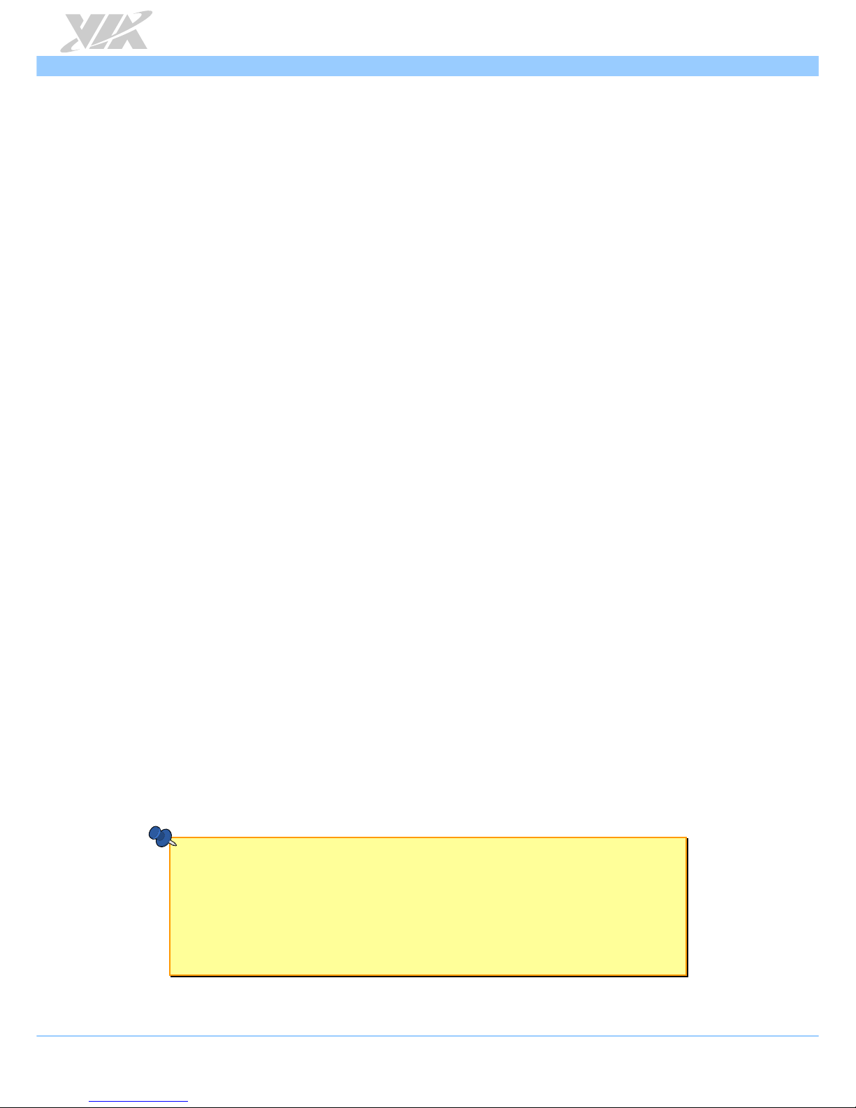
1.3. Layout Diagram
Figure 1: Layout diagram of VAB-1000 (top and bottom view)
Page 14

VAB-1000 User Manual
5
Item Description
1 DDR3 SDRAM
2 JM3: Miscellaneous jumper
3 PWR1: SATA power connector
4 CN9: SPI and GPIO pin header
5 WLAN1: USB 2.0 connector
6 CN8: COM and I²C pin header
7 JSF1: SPI flash connector
8 CN7: Front panel, USB 2.0 and COM pin header
9 SATA1: SATA connector
10 CN6: Front audio pin header
11 4GB eMMC flash memory
12 MPCIE_SET1: miniPCIe revision jumper
13 JM1: Clear CMOS jumper
14 VGA1: VGA pin header
15 BAT1: RTC battery connector
16 1.0GHz VIA Elite E1000 Cortex-A9 dual-core SoC
17 PBL_SET1: Backlight power jumper
18 PVDD_SET1: Panel power jumper
19 MPCIE1: miniPCIe slot
20 JTAG1: JTAG connector
21 DDR3 SDRAM
22 LVDS1: LVDS panel connector
Table 1: Layout diagram description table of VAB-1000
Page 15
VAB-1000 User Manual
6
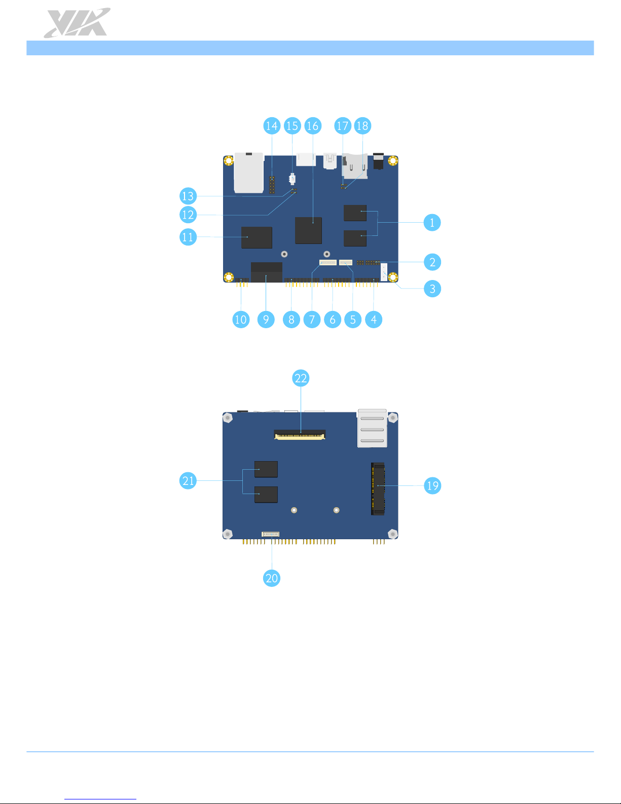
1.4. Product Dimensions
Figure 2: Dimensions of VAB-1000
Page 16
VAB-1000 User Manual
7
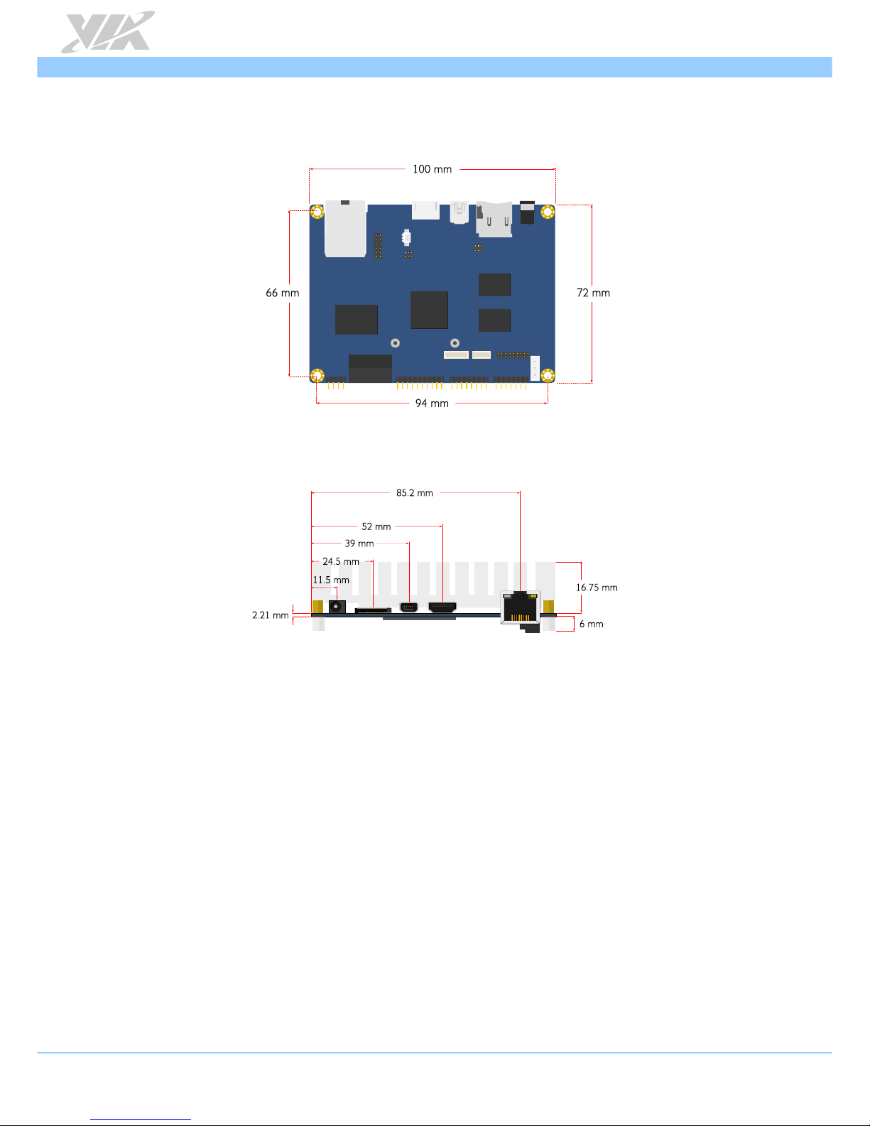
1.5. Height Distribution
Figure 3: Height distribution of VAB-1000 (top and bottom)
Page 17
VAB-1000 User Manual
8
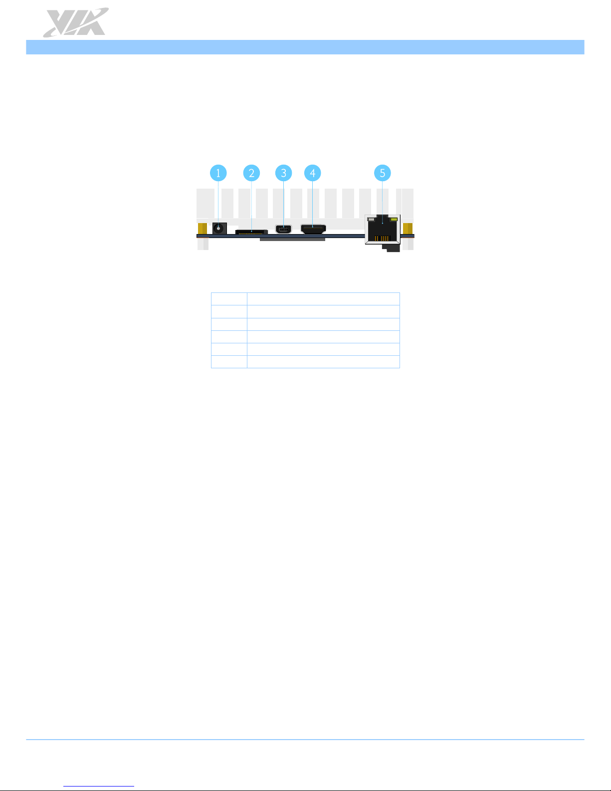
2. I/O Interface
The VIA VAB-1000 has a wide selection of interfaces integrated into the board. It includes a selection of
frequently used ports as part of the back panel I/O.
2.1. External I/O Ports
Figure 4: Back panel I/O
Item Description
1 CN1: DC-in jack
2 SD1: Micro SD card slot
3 USB1: Mini USB 2.0 port
4 HDMIO1: Mini HDMI port
5 LAN1: Gigabit Ethernet port
Table 2: Layout diagram description table of back paneI I/O
Page 18
VAB-1000 User Manual
9
2.1.1. DC-In Jack
The VAB-1000 comes with a DC-in jack on the back panel adjacent to the Micro SD slot. The DC-in jack
carriers 12V DC external power input. The specifications and pinout of power DC-in jack are shown
below.
Figure 5: DC-in jack diagram
Physical Specifications
Outer Diameter 3.7 mm
Inner Diameter 1.3 mm
Barrel Depth 8.25 mm
Electrical Specifications
Input Voltage 12V
Table 3: DC-in jack specifications
2.1.2. Micro SD Card Slot
The VAB-1000 comes with a Micro SD card slot located on the back panel. Micro SD card slot offers
expandable storage up to 32GB.
Figure 6: Micro SD card slot diagram
Pin Signal
1 SD0DATA2
2 SD0DATA3
3 SD0CMD
4 VDD (3.3V)
5 SD0CLK
6 GND
7 SD0DATA0
8 SD0DATA1
9 SD0_CD
Table 4: Micro SD card slot pinout
Page 19
VAB-1000 User Manual
10
2.1.3. Mini USB 2.0 Port
The VAB-1000 is equipped with a Mini USB 2.0 port located on the back panel. The Mini USB 2.0 interface
port gives complete Plug and Play and hot swap capability for external devices and it complies with USB
UHCI, rev. 2.0. The Mini USB 2.0 port uses the USB Type AB receptacle port connector. The pinout of the
Mini USB 2.0 port is shown below.
Figure 7: Mini USB 2.0 port diagram
Pin Signal
1 VCC (+5V)
2 USBH13 USBH1+
4 ID (GND)
5 GND
Table 5: Mini USB 2.0 port pinout
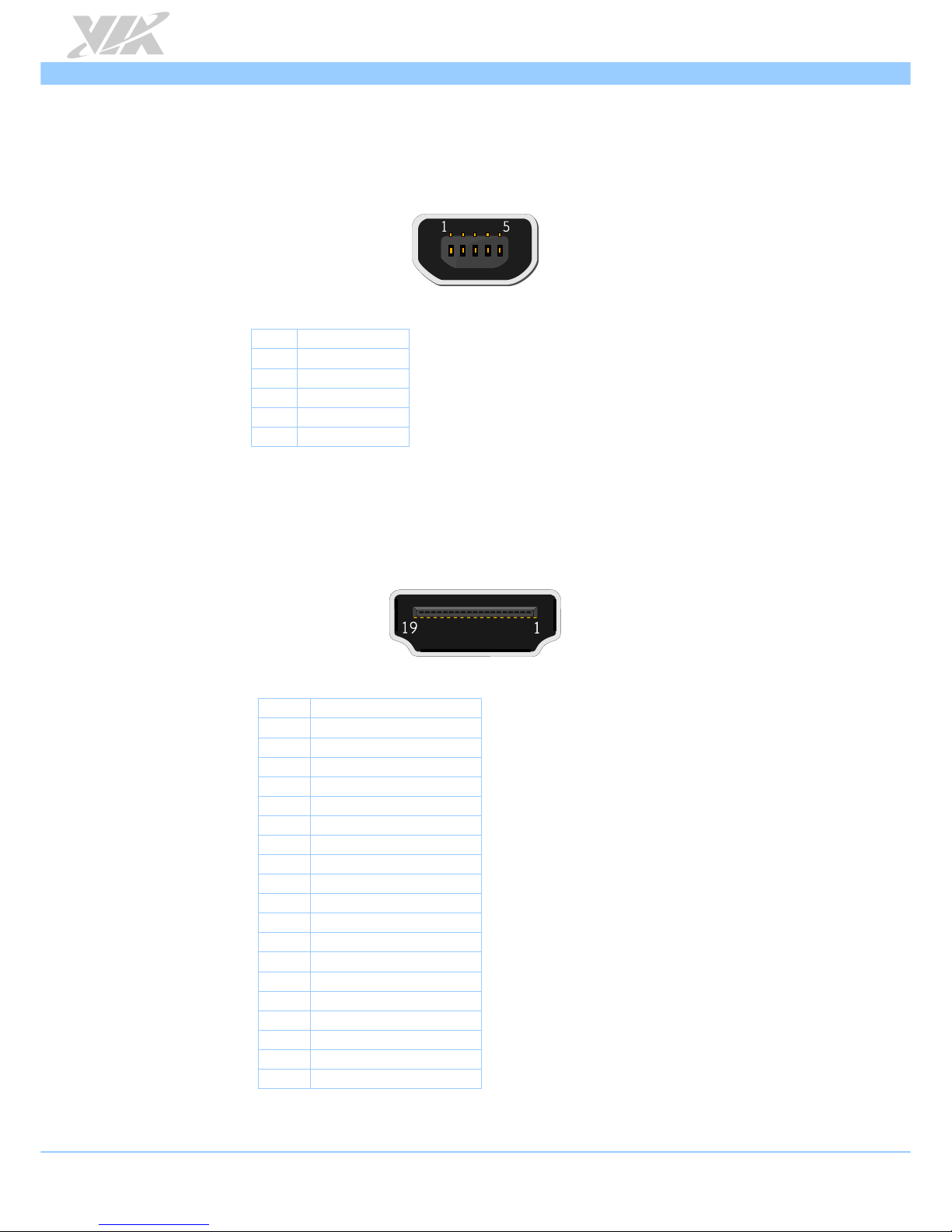
2.1.4. Mini HDMI
®
Port
The VAB-1000 has Mini HDMI port on the back panel. The Mini HDMI port uses an HDMI Type C
receptacle connector. It is used to connect high definition video and digital audio using a single cable.
The pinout of the Mini HDMI port is shown below.
Figure 8: Mini HDMI port diagram
Pin Signal
1 TMDS Data2 Shield
2 TMDS Data2+
3 TMDS Data24 TMDS Data1 Shield
5 TMDS Data1+
6 TMDS Data17 TMDS Data0 Shield
8 TMDS Data0+
9 TMDS Data010 TMDS Clock Shield
11 TMDS Clock+
12 TMDS Clock13 DDC/CEC Ground
14 CEC
15 SCL
16 SDA
17 Reserved
18 +5V Power
19 Hot Plug Detect
Table 6: Mini HDMI port pinout
Page 20
VAB-1000 User Manual
11
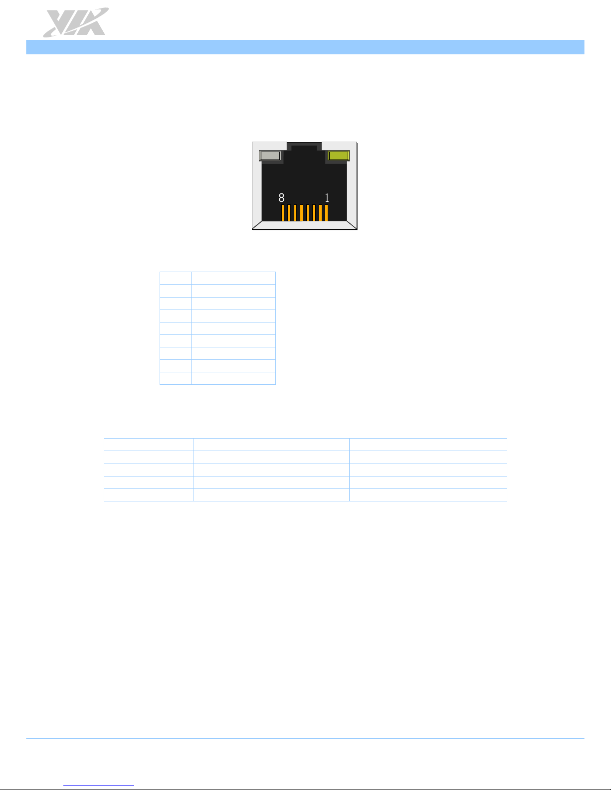
2.1.5. Gigabit Ethernet Port
The VAB-1000 is equipped with a Gigabit Ethernet port. The Gigabit Ethernet port is using 8 Position 8
Contact (8P8C) receptacle connector or commonly referred to as RJ-45. It is fully compliant with IEEE
802.3 (10BASE-T), 802.3u (100BASE-TX), and 802.3ab (1000BASE-T) standards. The pinout of the Gigabit
Ethernet port is shown below.
Figure 9: Gigabit Ethernet port diagram
Pin Signal
1 LAN1_TD0+
2 LAN1_TD03 LAN1_TD1+
4 LAN1_TD15 LAN1_TD2+
6 LAN1_TD27 LAN1_TD3+
8 LAN1_TD3-
Table 7: Gigabit Ethernet port pinout
The Gigabit Ethernet port has two individual LED indicators located on the front side to show its
Active/Link status and Speed status.
Left LED Right LED
Link Off LED is Off LED is Off
Speed_10Mbit The LED is On in Green color (flash)
LED is Off
Speed_100Mbit The LED is On in Red color (flash) LED is Off
Speed_1000Mbit LED is Off The LED is On in Orange color(flash)
Table 8: Gigabit Ethernet port LED color definition
Page 21
VAB-1000 User Manual
12
2.2. Onboard Connectors
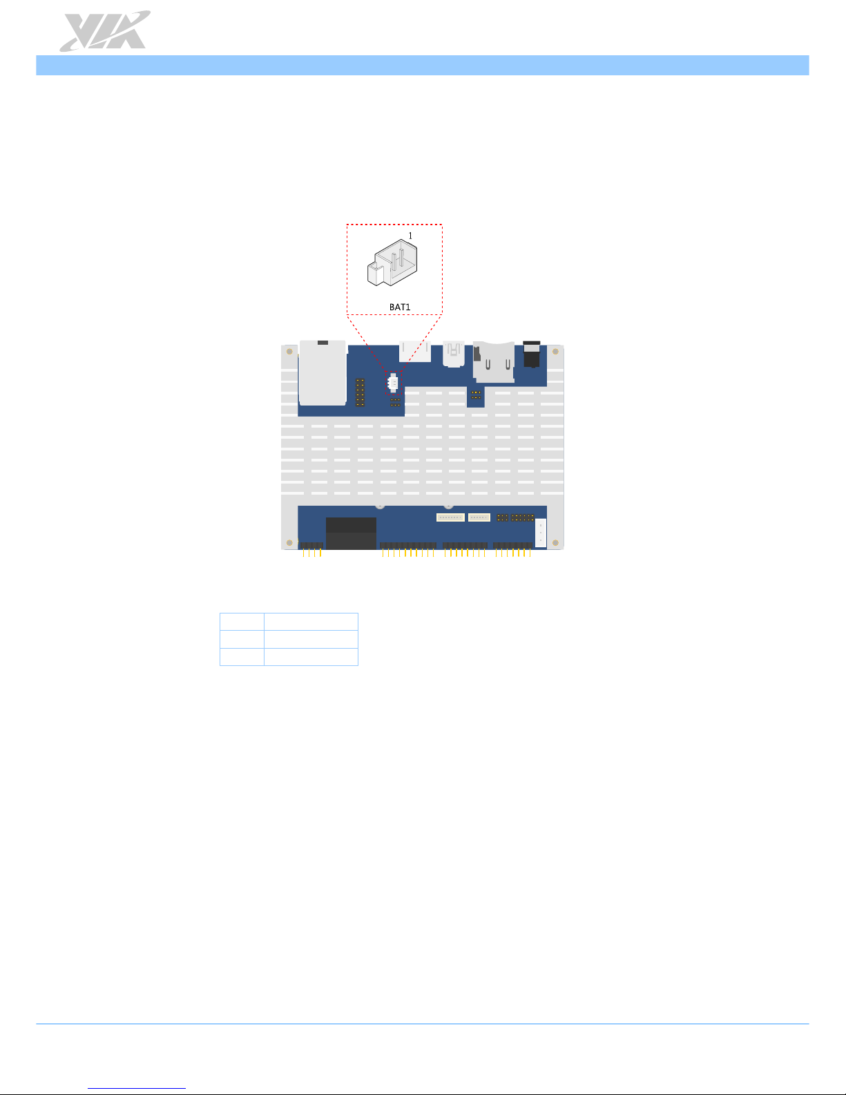
2.2.1. RTC Battery Connector
The VAB-1000 is equipped with an onboard RTC battery connector which is used for connecting the
external cable battery that provides power to the 32.768KHz crystal oscillator for Real Time Clock (RTC).
The RTC battery connector is labeled as “BAT1”. The connector pinout is shown below.
Figure 10: RTC battery connector diagram
Pin Signal
1 VBAT
2 GND
Table 9: RTC battery connector pinout
Page 22

VAB-1000 User Manual
13
2.2.2. SATA Connector
The SATA connector on board can support up to 3Gb/s transfer speeds. The SATA connector is labeled
as “SATA1” and it can support 2.5” SATA SSD. The pinout of the SATA connector is shown below.
Figure 11: SATA connector diagram
Pin Signal
1 GND
2 STXP_1
3 STXN_1
4 GND
5 SRXN_1
6 SRXP_1
7 GND
Table 10: SATA connector pinout
Page 23

VAB-1000 User Manual
14
2.2.3. SATA Power Connector
The SATA power connector is used for connecting the SATA SSD power cable to power the 2.5” SATA
SSD. When connecting the SATA SSD power cable, make sure the power plug is inserted in the proper
orientation and pins are properly aligned. The SATA power connector is labeled as “PWR1”. The pinout
of the SATA power connector is shown below.
Figure 12: SATA power connector diagram
Pin Signal
1 VDD5V
2 VDD12V
3 GND
Table 11: SATA power connector pinout
Page 24

VAB-1000 User Manual
15
2.2.4. SPI Flash Connector
The VAB-1000 has one 8-pin SPI flash connector. The SPI (Serial Peripheral Interface) flash connector is
used to update the Boot Loader EEPROM. The connector is labeled as “JSF1”. The pinout of the connector
is shown below.
Figure 13: SPI flash connector diagram
Pin Signal Pin Signal
1 VDD33_SF (VDD33_SPI VDD) 2 GND
3 SF_CS0- 4 SF_CLK
5 SF_MISO 6 SF_MOSI
7 NC 8 NC
Table 12: SPI flash connector pinout
Note:
NC represents “No Connection”
Page 25

VAB-1000 User Manual
16
2.2.5. USB 2.0 Connector
The VAB-1000 has an onboard USB 2.0 connector designed for connecting the USB Wi-Fi module. The
USB 2.0 connector is labeled as “WLAN1”. The pinout of USB 2.0 connector is shown below.
Figure 14: USB 2.0 connector diagram
Pin Signal
1 NC
2 WLAN_LED
3 GND
4 USBH1_C_2DP_1
5 USBH1_C_20M_1
6 VCC_USB1
Table 13: USB 2.0 connector pinout
Note:
The onboard USB 2.0 connector (WLAN1) shares the same USB signals with miniPCIe slot. Whenever the USB
2.0 connector is connected or in used, the miniPCIe slot is automatically disabled and vice versa. Please refer to
section 3.5 “Miscellaneous Jumper” for details about selecting the USB 2.0 connector/miniPCIe slot.
Page 26

VAB-1000 User Manual
17
2.2.6. VGA Pin Header
The mainboard has VGA pin header for CRT display. The VGA pin header is labeled as “VGA1”. The
pinout of the VGA pin header is shown below.
Figure 15: VGA pin header diagram
Pin Signal Pin Signal
1 VGA_R 2 +5VCRT
3 VGA_G 4 GND
5 VGA_B 6 VGA_SDA
7 GND 8 VGA_SCL
9 NC 10 VGA_VSYNC
11 VGA_HSYNC 12 GND
Table 14: VGA pin header pinout
Note:
This function is reserved for factory production only.
Page 27

VAB-1000 User Manual
18
2.2.7. Front Audio Pin Header
The VAB-1000 has a front audio pin header for connecting the Line-out, Line-in and Mic-in jacks. The pin
header is labeled as “CN6”. The pinout of the front audio pin header is shown below.
Figure 16: Front audio pin header diagram
Pin Signal Pin Signal
1 LINEIN_R 2 AUD_GND
3 LINEIN_L 4 MICIN1
5 LINEOUT_R 6 MICIN2
7 LINEOUT_L 8 HP_DET-
Table 15: Front audio pin header pinout
Page 28

VAB-1000 User Manual
19
2.2.8. Front Panel, USB 2.0 and COM Pin Header
The mainboard includes one Front panel, USB 2.0 and COM pin header block labeled as “CN7”. The Front
panel, USB 2.0 and COM pin header is used to connect the power button, two USB 2.0 ports, COM
(TX/RX) port and two activity LED indicators. The pinout of the pin header is shown below.
Figure 17: Front panel, USB 2.0 and COM pin header diagram
Pin Signal Pin Signal
1 PWR_LED (Series 470 ohm resistance) 2 VDD33_SUS/0.5A
3 PWR_BUTTON# 4 GND
5 RESET_GD 6 GND
7 -HD_LED1 (Series 470 ohm resistance) 8 VDD50/0.5A
9 VCC_USB2/0.5A 10 VCC_USB3/0.5A
11 USBH2_C_DM 12 USBH3_C_DM
13 USBH2_C_DP 14 USBH3_C_DP
15 GND 16 GND
17 DTE1_TXD_C 18 DTE1_RXD_C
19 HWTP_1 20 USBH123_SW
Table 16: Front panel, USB 2.0 and COM pin header pinout
Page 29

VAB-1000 User Manual
20
2.2.9. COM and I
²
C Pin Header
The COM and I²C pin header block labeled as “CN8” is used for connecting I²C devices and additional
COM port that supports TX/RX. The pinout of the COM and I²C pin header is shown below.
Figure 18: COM and I²C pin header diagram
Pin Signal Pin Signal
1 VDD33_SUS/0.5A 2 VDD33/0.5A
3 DTE0_TXD_C 4 NC
5 DTE0_RXD_C 6 NC
7 GND 8 I²C0_SCL(IPU to VDD33)
9 DTE2_TXD_C 10 I²C0_SDA(IPU to VDD33)
11 DTE2_RXD_C 12 I²C1_SCL(IPU to VDD33)
13 GND 14 I²C1_SDA(IPU to VDD33)
15 PMIC_CONF_SCL 16 PMIC_CONF_SDA
Table 17: COM and I²C pin header pinout
Page 30

VAB-1000 User Manual
21
2.2.10. SPI and GPIO Pin Header
The SPI and GPIO pin header block labeled as “CN9” is used for connecting the SPI device, and General
Purpose Input and Output. The pinout of the pin header is shown below.
Figure 19: SPI and GPIO pin header diagram
Pin Signal Pin Signal
1 VDD3318_DVP (for GFX GPIO
Power)/100mA
2 VDD50_SUS/0.5A
3 GND 4 VDD33 (for GPIO Power)/0.5A
5 NC 6 SPI1_CLK : SPI1 Host Interface
Clock GPIO5
7 NC 8 SPI1_MISO : SPI1 Host Interface
Master Input, Slave Output GPIO6
9 NC 10 SPI1_MOSI :SPI1 Host Interface
Master Output, Slave Input GPIO7
11 NC 12 SPI1 Host Interface Slave Select
Active-low. GPIO8
13 GND 14 GND
Table 18: SPI and GPIO pin header pinout
Note:
NC represents “No Connection”
Page 31

VAB-1000 User Manual
22
2.2.11. JTAG Connector
The JTAG connector provides a set of JTAG signals that allow JTAG debugging equipment to be used.
The connector is labeled as “JTAG1”. The pinout of the JTAG connector is shown below.
Figure 20: JTAG connector diagram
Pin Signal Pin Signal
1 GND 2 NC
3 JTAG_TRST# 4 JTAG_TD0
5 JTAG_TDI 6 JTAG_TMS
7 JTAG_TCK 8 VDD33
Table 19: JTAG connector pinout
Page 32

VAB-1000 User Manual
23
2.2.12. LVDS Panel Connector
The VAB-1000 has one LVDS panel connector on the bottom side of the board. The LVDS panel
connector can connect the panel’s LVDS cable to support the dual-channel 18/24-bit display. The LVDS
panel connector is labeled as “LVDS1”. The pinout of the LVDS panel connector is shown below.
Figure 21: LVDS panel connector diagram
Pin Signal Pin Signal
1 PVDD1 (for Panel VDD +5V or +3.3V) 2 PVDD1 (for Panel VDD +5V or +3.3V)
3 PVDD1 (for Panel VDD +5V or +3.3V) 4 VDD50
5 VDD50 6 VDD_BL (for Panel BL +12V or +5V)
7 VDD_BL (for Panel BL +12V or +5V) 8 VDD_BL (for Panel BL +12V or +5V)
9 GND 10 A0M1
11 A0P1 12 GND
13 A1M1 14 A1P1
15 GND 16 A2M1
17 A2P1 18 GND
19 A3M1 20 A3P1
21 GND 22 CLK1M1
23 CLK1P1 24 GND
25 A4M1 26 A4P1
27 GND 28 A5M1
29 A5P1 30 GND
31 A6M1 32 A6P1
33 GND 34 A7M1
35 A7P1 36 GND
37 CLK2M1 38 CLK2P1
39 VDD33 for EDID Power 40 LCD_CLK (I²C CLK)
41 LCD_DATA (I²C DATA) 42 ENABLT1 (Enable BL)
43 BAK_ADJ 44 NC
45 NC 46 NC
47 NC 48 NC
49 NC 50 NC
Table 20: LVDS panel connector pinout
Page 33

VAB-1000 User Manual
24
3. Jumpers
Jumper Description
A jumper consists of pair conductive pins used to close in or bypass an electronic circuit to set up or
configure particular feature using a jumper cap. The jumper cap is a small metal clip covered by plastic. It
performs like a connecting bridge to short (connect) the pair of pins. The usual colors of the jumper cap
are black/red/blue/white/yellow.
Jumper Setting
There are two settings of the jumper pin: “Short and Open”. The pins are “Short” when a jumper cap is
placed on the pair of pins. The pins are ”Open” if the jumper cap is removed.
In addition, there are jumpers that have three or more pins, and some pins are arranged in series. In case
of a jumper with three pins, place the jumper cap on pin 1 and pin 2 or pin 2 and 3 to Short it.
Some jumper size is small or mounted on the crowded location of the board that makes it difficult to
access. Therefore, using long-nose pliers in installing and removing the jumper cap is very helpful.
Figure 22: Jumper settings example
Caution:
Make sure to install the jumper cap on the correct pins. Installing it in the wrong pin might cause damage and
malfunction.
Page 34

VAB-1000 User Manual
25
3.1. Backlight Power Jumper
The mainboard has a jumper that controls the input voltage delivered to the LVDS backlight connector.
The jumper is labeled as “PBL_SET1”. The jumper settings are shown below.
Figure 23: Backlight power jumper diagram
Settings Pin 1 Pin 2 Pin 3
+12V (Default) Short Short Open
+5V Open Short Short
Table 21: Backlight power jumper settings
3.2. Panel Power Jumper
The mainboard has a jumper that controls the voltage delivered to the LVDS panel connector. The jumper
is labeled as “PVDD_SET1”. The jumper settings are shown below.
Figure 24: Panel power jumper diagram
Settings Pin 1 Pin 2 Pin 3
+5V Short Short Open
+3.3V (Default) Open Short Short
Table 22: Panel power jumper settings
Page 35

VAB-1000 User Manual
26
3.3. Clear CMOS Jumper
The onboard CMOS RAM stores system configuration data and has an onboard battery power supply. To
reset the CMOS settings, set the jumper on pins 2 and 3 while the system is off. Return the jumper to pins
1 and 2 afterwards. Setting the jumper while the system is on will damage the mainboard. The jumper is
labeled as “JM1”. The default setting is on pins 1 and 2.
Figure 25: Clear CMOS jumper diagram
Settings Pin 1 Pin 2 Pin 3
Normal (default) Short Short Open
Clear CMOS Open Short Short
Table 23: Clear CMOS jumper settings
Note:
Except when clearing the CMOS RAM, never remove the cap from the JM1 (Clear CMOS) jumper default
position. Removing the cap will cause system boot failure. Avoid clearing the CMOS while the system is on; it
will damage the mainboard.
Page 36

VAB-1000 User Manual
27
3.4. MiniPCIe Revision Jumper
The mainboard has a miniPCIe revision jumper that determines the supported revision specification of
miniPCIe slot. The jumper is labeled as “MPCIE_SET1”. The jumper settings are shown below.
Figure 26: MiniPCIe revision jumper diagram
Settings Pin 1 Pin 2 Pin 3
Support Revision 1.2 (Default) Short Short Open
Support Revision 1.1 Open Short Short
Table 24: MiniPCIe revision jumper settings
Page 37

VAB-1000 User Manual
28
3.5. Miscellaneous Jumper
The mainboard has a miscellaneous jumper that is used to enable/disable the SD card write protect,
detect the active/inactive audio head phone, select the USB bus and auto power-on function. The jumper
is labeled as “JM3”. The jumper settings are shown below.
Figure 27: Miscellaneous jumper diagram
SD Card Write Protect Settings Pin 1-2
Disable (Default) Short
Enable Open
Reserved Pin 3-4
(Default) Short
Open
Audio Head Phone Detect Settings Pin 5-6
Active (Default) Short
Inactive Open
USB Bus Selection Settings Pin 7-8
USB to miniPCIe (Default) Short
USB to WLAN Open
Auto Power On Function by H/W Settings Pin 9-10
Enable (Default) Short
Disable Open
Table 25: Miscellaneous jumper settings
Note:
In order to enable the Watchdog timer function, Auto Power On Function must be enabled first.
Page 38

VAB-1000 User Manual
29
4. Hardware Installation
4.1. Installing into a Chassis
The VAB-1000 board can be fitted into any chassis that has the mounting holes for compatible with the
standard Pico-ITX mounting hole locations. Additionally, the chassis must meet the minimum height
requirements for specified areas of the board. If the VAB-1000-T I/O card is being used, the chassis will
need to accommodate the additional space requirements.
4.1.1. Suggested minimum chassis dimensions
The figure below shows the suggested minimum space requirements that a chassis should have in order to
work well with the VAB-1000 board.
Figure 28: Suggested minimum chassis dimensions
Each side of the board should have a buffer zone from the internal wall of the chassis. The side of the
board that accommodates the I/O coastline should have a buffer of 1.5mm. The side on the opposite end
of the I/O coastline that has SATA connector and board-to-board pin headers should have a buffer of at
least 12mm, or 27mm if the VAB-1000-T I/O card will be used. The two sides adjacent to the I/O
coastline should have at least a 2mm buffer.
Page 39

VAB-1000 User Manual
30
4.1.2. Suggested minimum chassis height
The figure below shows the suggested minimum height requirements for the internal space of the chassis.
It is not necessary for the internal ceiling to be evenly flat. What is required is that the internal ceiling
height must be strictly observed for each section that is highlighted.
Figure 29: Suggested minimum internal chassis ceiling height
Note:
In getting the minimum height requirements for internal space of the chassis, it is required to consider the
heights of the onboard connectors (such as JTAG connector and miniPCIe slot) on the bottom side of the VAB1000 board.
Page 40

VAB-1000 User Manual
31
4.1.3. Suggested keep out areas
The figure below shows the areas of the mainboard that is highly suggested to leave unobstructed.
Figure 30: Suggested keep out areas
Page 41

VAB-1000 User Manual
32
5. Software and Technical Supports
5.1. Android Support
The VAB-1000 Board Support Package features Android 4.4.2 operating system as well as the VIA Smart
ETK comprising a number of APIs.
5.2. Technical Supports and Assistance
For utilities downloads, latest documentation and new information about the VAB-1000, go to
https://www.viatech.com/en/boards/pico-itx/vab-1000/
For technical support and additional assistance, always contact your local sales representative or
board distributor, or go to
http://www.viatech.com/en/about/contact/
to fill up the form request.
For OEM clients and system integrators developing a product for long term production, other code
and resources may also be made available. Contact VIA to submit a request.
Page 42

VAB-1000 User Manual
33
Appendix A. VAB-1000-T I/O Card
A.1. Specifications
Front Panel I/O
3 x Audio jacks (Line-in, Line-out and Mic-in)
1 x SSD activity LED indicator
1 x USB/COM LED indicator
2 x USB 2.0 ports
1 x Power on/off button with built-in LED
Supports three modes:
System Suspend/Resume (press the button once)
Popup power control menu (press the button for 4 seconds)
System Off (press the button for 8 seconds)
Onboard Connectors and Jumper
1 x Front panel, USB 2.0 and COM board-to-board connector
1 x Audio board-to-board connector
1 x COM pin header (for RS-232/Console)
1 x USB/COM jumper
Dimensions
100mm x 21mm
Page 43

VAB-1000 User Manual
34
A.2. Layout Diagram
Figure 31: VAB-1000-T layout
Item Description
1 PW_SW: Power on/off button with built-in LED
2 HD_LED: SSD activity LED indicator
3 USB/COM_LED: USB/COM indicator LED
4 USB2: USB 2.0 port
5 USB1: USB 2.0 port
6 LINE-IN: Line-in jack
7 LINE-OUT: Line-out jack
8 MIC-IN: Mic-in jack
9 COM1: COM pin header
10 B2B_AUDIO: Audio board-to-board connector
11 B2B_FRONT_USB_COM: Front panel, USB 2.0 and
COM board-to-board connector
12 USB_COM_SEL: USB/COM jumper
Table 26: Layout diagram description table of VAB-1000-T
A.3. Dimensions
Figure 32: VAB-1000-T dimensions
Page 44

VAB-1000 User Manual
35
A.4. Onboard Connectors and Jumper
A.4.1. Audio Board-to-Board Connector
Figure 33: Audio board-to-board connector diagram
Pin Signal Pin Signal
1 LINEIN_R 2 GND_AUDIO
3 LINEIN_L 4 MICIN1
5 LINEOUT_R 6 MINI2
7 LINEOUT_L 8 HP_DET-
Table 27: Audio board-to-board connector pinout
A.4.2. Front Panel, USB 2.0 and COM Board-to-Board Connector
Figure 34: Front panel, USB 2.0 and COM board-to-board connector diagram
Page 45

VAB-1000 User Manual
36
Pin Signal Pin Signal
1 PWR_LED 2 VDD33_SUS
3 PWR_BUTTON- 4 GND
5 RESET_GND 6 GND
7 -HD_LED1 8 VDD50
9 VCC_USB2 10 VCC_USB3
11 USBH2_C_DM 12 USBH3_C_DM
13 USBH2_C_DP 14 USBH3_C_DP
15 GND 16 GND
17 DTE1_TXD_C 18 DTE1_RXD_C
19 HWTP_1 20 USBH123_SW
Table 28: Front panel, USB 2.0 and COM board-to-board connector pinout
A.4.3. COM Pin Header
Figure 35: COM pin header diagram
Pin Signal
1 DTE1_TXD
2 DTE1_RXD_C
3 GND
Table 29: COM pin header pinout
Note:
Please use the Console cable provided for connection.
Page 46

VAB-1000 User Manual
37
A.4.4. USB/COM Jumper
Figure 36: USB/COM jumper diagram
Settings Pin 1 Pin 2 Pin 3
USB (Default) Short Short Open
COM (TX/RX) Open Short Short
Table 30: USB/COM jumper settings
Page 47

VAB-1000 User Manual
38
Appendix B. VAB-1000-L LVDS Converter Card
B.1. Specifications
Onboard Connectors
1 x Board-to-Board LVDS connector
1 x 1-Channel LVDS panel connector
1 x 1-Channel Backlight connector
1 x 2-Channel LVDS panel connector
1 x 2-Channel Backlight connector
1 x DC-in connector
Dimensions
68mm x 47mm
B.2. Layout Diagram
1
1
1
DC-in connector
2-Channel LVDS panel connector
2-Channel Backlight connector
1-Channel LVDS panel connector
Figure 37: VAB-1000-L layout (top side)
1
1
2-Channel Backlight connector
Board-to Board LVDS connector
Figure 38: VAB-1000-L layout (bottom side)
Page 48

VAB-1000 User Manual
39
B.3. Dimensions
Figure 39: VAB-1000-L dimensions (top view)
Figure 40: VAB-1000-L dimensions (side view)
Page 49

VAB-1000 User Manual
40
B.4. VAB-1000-L Onboard Connectors
B.4.1. Board-to-Board LVDS Connector
Figure 41: Board-to-board LVDS connector diagram
Pin Signal Pin Signal
1 GND 2 NC
3 NC 4 NC
5 NC 6 NC
7 NC 8 BAK_ADJ
9 ENABLT1 10 LCD_DATA
11 LCD_CLK 12 VDD33
13 CLK2P1 14 CLK2M1
15 GND 16 A7P1
17 A7M1 18 GND
19 A6P1 20 A6M1
21 GND 22 A5P1
23 A5M1 24 GND
25 A4P1 26 A4M1
27 GND 28 CLK1P1
29 CLK1M1 30 GND
31 A3P1 32 A3M1
33 GND 34 A2P1
35 A2M1 36 GND
37 A1P1 38 A1M1
39 GND 40 A0P1
41 A0M1 42 GND
43 VDD_BL 44 VDD_BL
45 VDD_BL 46 VDD50
47 VDD50 48 PVDD1
49 PVDD1 50 PVDD1
Table 31: Board-to-board LVDS connector pinout
Page 50

VAB-1000 User Manual
41
B.4.2. 2-Channel LVDS Panel Connector
Figure 42: 2-Channel LVDS panel connector diagram
Pin Signal Pin Signal
1 2CH_1LDC4- 2 PVDD1
3 2CH_1LDC4+ 4 PVDD1
5 GND 6 GND
7 2CH_1LDC5- 8 GND
9 2CH_1LDC5+ 10 2CH_1LDC011 GND 12 2CH_1LDC0+
13 2CH_1LDC6- 14 GND
15 2CH_1LDC6+ 16 2CH_1LDC117 GND 18 2CH_1LDC1+
19 2CH_1LCLK2- 20 GND
21 2CH_1LCLK2+ 22 2CH_1LDC223 GND 24 2CH_1LDC2+
25 2CH_1LDC7- 26 GND
27 2CH_1LDC7+ 28 2CH_1LCLK129 NC 30 2CH_1LCLK1+
31 GND 32 GND
33 +3.3V 34 2CH_1LDC335 NC 36 2CH_1LDC3+
37 Reserved 38 LCD_CLK
39 SEL68 40 LCD_DAT
Table 32: 2-Channel LVDS panel connector pinout
Page 51

VAB-1000 User Manual
42
B.4.3. 1-Channel LVDS Panel Connector
Figure 43: 1-Channel LVDS panel connector diagram
Pin Signal Pin Signal
1 NC 2 PVDD1
3 PVDD1 4 GND
5 GND 6 NC
7 1CH_1LDC0+ 8 1CH_1LDC0-
9 GND 10 1CH_1LDC1+
11 1CH_1LDC1- 12 GND
13 1CH_1LDC2+ 14 1CH_1LDC2-
15 GND 16 1CH_1LCLK1+
17 1CH_1LCK1- 18 GND
19 1CH_1LDC3+ 20 1CH_1LDC3-
21 GND 22 NC
23 NC 24 GND
25 NC 26 PVDD1
27 NC 28 NC
29 NC 30 NC
Table 33: 1-Channel LVDS panel connector pinout
Page 52

VAB-1000 User Manual
43
B.4.4. 2-Channel Backlight Connector
Figure 44: 2-Channel backlight connector diagram
Pin Signal Pin Signal
1 VDD_BL_C 2 VDD_BL_C
3 ENABLT1 4 NC
5 NC 6 BL_CTL
7 GND 8 GND
Table 34: 2-Channel backlight connector pinout
B.4.5. 1-Channel Backlight Connector
Figure 45: 1-Channel backlight connector diagram
Pin Signal Pin Signal
1 NC 2 NC
3 BAK_ADJ 4 ENABLT1
5 NC 6 NC
7 NC 8 GND
9 GND 10 VDD_BL_C
11 VDD_BL_C 12 VDD_BL_C
Table 35: 1-Channel backlight connector pinout
Page 53

VAB-1000 User Manual
44
B.4.6. DC-in Connector
Figure 46: DC-in connector diagram
Pin Signal
1 GND
2 DCIN
Table 36: DC-in connector pinout
Note:
A panel that carries voltage lower than 12V does not need to externally connect to a DC-in connector.
Page 54

VAB-1000 User Manual
45
Appendix C. Installing I/O Expansion Card
C.1. Installing the VAB-1000-T I/O Card
The VAB-1000 board comes with a VAB-1000-T I/O card. The VAB-1000-T I/O card is an extender card,
which adds multiple I/O interfaces, including audio jacks, USB 2.0 ports, LED indicators, power on/off
button and COM pin header for one COM port (TX/RX support only) as well as board-to-board
connectors.
Step 1
Align the Audio and Front panel, USB 2.0 and COM board-to-board connectors on the VAB-1000-T I/O
card with the CN6 and CN7 pin header block on the VAB-1000 board.
Figure 47: Installing the VAB-1000-T I/O card
Step 2
Gently apply even pressure until the pins on the VAB-1000 board have been fully inserted into the Audio
and Front panel, USB 2.0, and COM board-to-board connectors of the VAB-1000-T I/O card.
Page 55

VAB-1000 User Manual
46
Step 3
Secure the VAB-1000-T I/O card to the standoffs with two screws.
Figure 48: Securing the VAB-1000-T I/O card
Page 56

VAB-1000 User Manual
47
C.2. Installing VAB-1000-L LVDS Converter Card (optional)
Step 1
Connect one end of the LVDS flat flex cable into the LVDS panel connector on the VAB-1000 board, then
connect the other end of the cable to the board-to-board LVDS connector on the VAB-1000-L LVDS
converter card.
VAB-1000-L (bottom side)
VAB-1000 (bottom side)
1
2
Figure 49: Connecting the LVDS flat flex cable
Step 2
Install the VAB-1000-L LVDS converter card to a suitable surface on the chassis and secure it with two
screws.
2
1
C
casing
V
LVDS flat flex cable
Figure 50: Installing the VAB-1000-L LVDS converter card on the chassis
Page 57

VAB-1000 User Manual
48
Step 3
Connect the 2-Channel backlight cable into the 2-Channel backlight connector on the VAB-1000-L LVDS
converter card, and then connect the other end of the cable into the 10.4” LVDS panel display.
1
2
b /
o!!
Lo!"
#$"%
(&!#!'
Figure 51: Connecting the 2-Channel backlight cable
Page 58

VAB-1000 User Manual
49
Step 4
Connect the 2-Channel LVDS cable into the 2-Channel LVDS panel connector on the VAB-1000-L LVDS
converter card, and then connect the other end of the cable into the 10.4” LVDS panel display.
1
2
Figure 52: Connecting the 2-Channel LVDS cable
Page 59

VAB-1000 User Manual
50
Step 5
Connect the USB touch panel cable into the 10.4” LVDS panel display, and then connect the other end of
the cable into one of the USB 2.0 port on the VAB-1000 board.
1
2
Figure 53: Connecting the USB touch panel cable
Page 60

VAB-1000 User Manual
51
Step 4
Connect the DC-in cable into the DC-in connector on the VAB-1000-L LVDS converter card.
Figure 54: Connecting the DC-in cable
Page 61

VAB-1000 User Manual
52
Appendix D. Installing Wireless Accessories
This section provides information on how to install the optional wireless accessories to provide wireless
connection such as Wi-Fi, Bluetooth and 3G.
D.1. Installing the VNT9271 USB Wi-Fi Dongle
Step 1
Locate a USB 2.0 port on the front panel.
Step 2
Insert the VNT9271 dongle in one of the USB 2.0 port.
Figure 55: Inserting VNT9271 USB Wi-Fi dongle
Page 62

VAB-1000 User Manual
53
D.2. Installing the EMIO-1533 USB Wi-Fi Module
Step 1
Mount the EMIO-1533 module to the prepared standoff on the chassis. Align the two mounting holes on
the EMIO-1533 module with the mounting holes on the standoffs, then secure the EMIO-1533 module in
place with two screws.
1
2
Figure 56: Installing EMIO-1533 module
Step 2
Connect one end of the USB Wi-Fi cable to the onboard USB 2.0 connector (WLAN1), and then connect
the other end of the cable to the EMIO-1533 module.
2
1
Figure 57: Connecting the USB Wi-Fi cable diagram
Page 63

VAB-1000 User Manual
54
Step 3
Insert the Wi-Fi antenna cable into the antenna hole from the inside of the panel I/O plate. Insert the
toothed washer, fasten it with the nut and install the external antenna.
SS
SS
1
2
3
4
Panel I/O plate
Figure 58: Installing Wi-Fi antenna cable diagram
Step 4
Connect the other end of the Wi-Fi antenna cable to the micro-RF connector labeled “IPEX” on the EMIO1533 module.
Figure 59: Connecting the Wi-Fi antenna cable to EMIO-1533 module
Page 64

VAB-1000 User Manual
55
D.3. Installing the EMIO-1541 miniPCIe Wi-Fi Module
Step 1
Locate the miniPCIe slot and install the hex standoff screw provided.
Figure 60: Installing the hex standoff screw for EMIO-1541 module
Step 2
Align the notch on the EMIO-1541 module with the protruding wedge on the miniPCIe slot then insert the
module at 30° angle.
30
Figure 61: Installing the EMIO-1541 module
Page 65

VAB-1000 User Manual
56
Step 3
Once the module has been inserted, push down the module until the screw hole align with the mounting
hole on the hex standoff. Secure the module with screw to the standoff.
Figure 62: Securing the EMIO-1541 module
Step 4
Insert the Wi-Fi antenna cable into the antenna hole from inside of the chassis. Insert the washer, and
fasten it with the nut. Then install the external antenna.
SS
SS
1
2
3
4
Panel I/O plate
Figure 63: Installing the Wi-Fi antenna of EMIO-1541 module
Page 66

VAB-1000 User Manual
57
Step 5
Connect the other end of the Wi-Fi antenna cable onto the micro-RF connector labeled “TRX” on the
EMIO-1541 module.
Figure 64: Connecting the Wi-Fi antenna cable to EMIO-1541 module
Page 67

VAB-1000 User Manual
58
D.4. Installing the EMIO-2550 miniPCIe Mobile Broadband
Module
Step 1
Insert the SIM card on the bottom side of the EMIO-2550 module. (EMIO-2550-00A1)
Step 2
Locate the miniPCIe slot and install the hex standoff screw provided.
Figure 65: Installing the hex standoff screw for EMIO-2550 module
Step 3
Align the notch on the EMIO-2550 module with the protruding wedge on the miniPCIe slot then insert the
module at 30° angle.
30
Figure 66: Installing the EMIO-2550 module
Page 68

VAB-1000 User Manual
59
Step 4
Once the module has been inserted, push down the module until the screw hole align with the mounting
hole on the standoff. Secure the module with the screw to the standoff.
Figure 67: Securing the EMIO-2550 module
Step 5
Insert the 3G antenna cable into the antenna hole from the inside of the panel I/O plate. Insert the
toothed washer, fasten it with the nut and install the external 3G antenna.
SS
1
2
3
4
Panel I/O plate
Figure 68: Installing the 3G antenna cable diagram
Page 69

VAB-1000 User Manual
60
Step 6
Connect the other end of the 3G antenna cable onto the micro-RF connector labeled “MAN” on the
EMIO-2550 module.
Figure 69: Connecting the 3G antenna cable to EMIO-2550 module
Page 70

 Loading...