

Page 1

1.03-05242017-171300
USER MANUAL
QSM-8Q60
Qseven™ ARM module with
NXP i.MX 6QuadPlus or i.MX 6DualLite
Cortex-A9 SoC
Page 2

Copyright
Copyright © 2015-2017 VIA Technologies Incorporated. All rights reserved.
No part of this document may be reproduced, transmitted, transcribed, stored in a retrieval system, or translated into any language,
in any form or by any means, electronic, mechanical, magnetic, optical, chemical, manual or otherwise without the prior written
permission of VIA Technologies, Incorporated.
Trademarks
All trademarks are the property of their respective holders.
Disclaimer
No license is granted, implied or otherwise, under any patent or patent rights of VIA Technologies. VIA Technologies makes no
warranties, implied or otherwise, in regard to this document and to the products described in this document. The information
provided in this document is believed to be accurate and reliable as of the publication date of this document. However, VIA
Technologies assumes no responsibility for the use or misuse of the information (including use or connection of extra
device/equipment/add-on card) in this document and for any patent infringements that may arise from the use of this document. The
information and product specifications within this document are subject to change at any time, without notice and without obligation
to notify any person of such change.
VIA Technologies, Inc. reserves the right the make changes to the products described in this manual at any time without prior notice.
Regulatory Compliance
FCC-A Radio Frequency Interference Statement
This equipment has been tested and found to comply with the limits for a class A digital device, pursuant to part 15 of the FCC rules.
These limits are designed to provide reasonable protection against harmful interference when the equipment is operated in a
commercial environment. This equipment generates, uses, and can radiate radio frequency energy and, if not installed and used in
accordance with the instruction manual, may cause harmful interference to radio communications. Operation of this equipment in a
residential area is likely to cause harmful interference, in which case the user will be required to correct the interference at his
personal expense.
Notice 1
The changes or modifications not expressly approved by the party responsible for compliance could void the user's authority to
operate the equipment.
Notice 2
Shielded interface cables and A.C. power cord, if any, must be used in order to comply with the emission limits.
Notice 3
The product described in this document is designed for general use, VIA Technologies assumes no responsibility for the conflicts or
damages arising from incompatibility of the product. Check compatibility issue with your local sales representatives before placing
an order.
Page 3

Battery Recycling and Disposal
Only use the appropriate battery specified for this product.
Do not re-use, recharge, or reheat an old battery.
Do not attempt to force open the battery.
Do not discard used batteries with regular trash.
Discard used batteries according to local regulations.
Safety Precautions
Always read the safety instructions carefully.
Keep this User's Manual for future reference.
All cautions and warnings on the equipment should be noted.
Keep this equipment away from humidity.
Lay this equipment on a reliable flat surface before setting it up.
Make sure the voltage of the power source and adjust properly 110/220V before connecting the
equipment to the power inlet.
Place the power cord in such a way that people cannot step on it.
Always unplug the power cord before inserting any add-on card or module.
If any of the following situations arises, get the equipment checked by authorized service personnel:
The power cord or plug is damaged.
Liquid has penetrated into the equipment.
The equipment has been exposed to moisture.
The equipment has not worked well or you cannot get it work according to User's Manual.
The equipment has dropped and damaged.
The equipment has obvious sign of breakage.
Do not leave this equipment in an environment unconditioned or in a storage temperature above
70°C (158°F). The equipment may be damaged.
Do not leave this equipment in direct sunlight.
Never pour any liquid into the opening. Liquid can cause damage or electrical shock.
Do not place anything over the power cord.
Do not cover the ventilation holes. The openings on the enclosure protect the equipment from
overheating
Page 4

QSM-8Q60 User Manual
iv
Box Contents
QSM-8Q60-QP SKU
1 x QSM-8Q60 Qseven
™
module (with 1.0GHz NXP i.MX 6QuadPlus Cortex-A9 quad-core SoC)
1 x QSM-8Q60 evaluation carrier board (QSMDB2)
1 x DC power cable
1 x Console cable
QSM-8Q60 SKU
1 x QSM-8Q60 Qseven
™
module (with 1.0GHz NXP i.MX DualLite Cortex-A9 dual-core SoC)
1 x QSM-8Q60 evaluation carrier board (QSMDB2)
1 x DC power cable
1 x Console cable
Ordering Information
Part Number Description
10GEC10H40020
Qseven™ module with 1.0GHz NXP i.MX 6QuadPlus Cortex-A9, 4GB
eMMC, 4MB SPI ROM, 2GB DDR3 SDRAM, HDMI, 4 x USB 2.0, USB OTG
client, LVDS, 3 x COM (TX/RX), Gigabit Ethernet, 10/100Mbps Ethernet,
2 x CAN bus, PCIe x1, Micro SD card slot
10GEC10700020
Qseven™ module with 1.0GHz NXP i.MX 6DualLite Cortex-A9, 4GB
eMMC, 4MB SPI ROM, 2GB DDR3 SDRAM, HDMI, 4 x USB 2.0, USB OTG
client, LVDS, 3 x COM (TX/RX), Gigabit Ethernet, 10/100Mbps Ethernet,
2 x CAN bus, PCIe x1, Micro SD card slot
10GFL00000020
QSM-8Q60 evaluation carrier board (QSMDB2) with CAN bus cable
and DC power cable
Optional Accessories
Wireless Modules
Part Number Description
00GO27100BU2B0D0
VNT9271BU0DB IEEE 802.11 b/g/n USB Wi-Fi dongle
EMIO-1541-00A1
VNT9485 IEEE 802.11 b/g/n miniPCIe Wi-Fi module with assembly kit
and antenna
EMIO-2531-00A1
VAB-820-W-M IEEE 802.11 b/g/n miniPCIe Wi-Fi & Bluetooth module
with assembly kit and antenna
EMIO-2550-00A1
3.75G HSPA/UMTS mobile broadband full size miniPCIe module with
GPS, SIM card slot, assembly kit and antenna
Page 5

QSM-8Q60 User Manual
v
Table of Contents
1. Product Overview ........................................................................................................................ 1
1.1. Key Features ........................................................................................................................................................ 1
1.2. Product Specifications ...................................................................................................................................... 2
1.3. Layout Diagram .................................................................................................................................................. 4
1.4. Product Dimensions .......................................................................................................................................... 5
2. Onboard Slot ................................................................................................................................ 6
2.1. Micro SD Card Slot ........................................................................................................................................... 6
3. Onboard Jumpers ......................................................................................................................... 7
3.1. Micro SD/SPI Boot Select Jumper .................................................................................................................. 8
4. Hardware Installation .................................................................................................................. 9
4.1. Installing the QSM-8Q60 Module on the QSMDB2 Carrier Board ........................................................ 9
5. Software and Technical Supports ........................................................................................... 12
5.1. Linux Support .................................................................................................................................................. 12
5.1.1. Driver Installation .................................................................................................................................... 12
5.2. Technical Supports and Assistance ............................................................................................................ 12
Appendix A. QSMDB2 Carrier Board Reference ........................................................................... 13
A.1. Board Specifications .......................................................................................................................................... 13
A.2. QSMDB2 External I/O Connectors ................................................................................................................ 14
A.2.1. Front Panel I/O ............................................................................................................................................ 14
A.3. QSMDB2 Layout Diagram................................................................................................................................. 14
A.3.1. QSMDB2 Onboard Connectors, Slots and Pin Headers ................................................................... 15
A.3.1.1. Qseven MXM Connector ................................................................................................................ 15
A.3.1.2. Audio Pin Header ............................................................................................................................. 18
A.3.1.3. Touch Panel Connector .................................................................................................................. 18
A.3.1.4. RTC Battery Connector ................................................................................................................... 19
A.3.1.5. DC-In Connector .............................................................................................................................. 19
A.3.1.6. COM Pin headers ............................................................................................................................. 20
A.3.1.7. Serial and I2C Pin Header ............................................................................................................... 21
A.3.1.8. CAN Bus Connector ........................................................................................................................ 22
A.3.1.9. GPIO Pin Header .............................................................................................................................. 23
A.3.1.10. LVDS Panel Connector ................................................................................................................. 24
A.3.1.11. LVDS Inverter Connector ............................................................................................................. 25
A.3.1.12. MiniPCIe Slot .................................................................................................................................. 26
A.3.1.13. SIM Card Slot .................................................................................................................................. 27
A.3.2. QSMDB2 Onboard Jumpers .................................................................................................................... 28
A.3.2.1. Backlight and Panel Power Select Jumper ................................................................................. 28
Appendix B. Installing Wireless Accessories ............................................................................... 29
B.1. Inserting VNT9271 USB Wi-Fi Dongle ........................................................................................................... 29
B.2. Installing EMIO-1541 miniPCIe Wi-Fi Module ............................................................................................. 30
B.3. Installing EMIO-2531 miniPCIe Wi-Fi + Bluetooth Module ..................................................................... 32
B.4. Installing EMIO-2550 miniPCIe Mobile Broadband Module .................................................................... 34
Appendix C. Inserting SIM Card...................................................................................................... 37
Page 6

QSM-8Q60 User Manual
vi
List of Figures
Figure 1: Layout diagram of the QSM-8Q60 (top side) ..............................................................................................4
Figure 2: Layout diagram of the QSM-8Q60 (bottom side) .......................................................................................4
Figure 3: Dimensions of the QSM-8Q60 module (top view) ....................................................................................5
Figure 4: Dimensions of the QSM-8Q60 attached to the carrier board (top view) .............................................5
Figure 5: Dimensions of the QSMDB2 external I/O .....................................................................................................5
Figure 6: Micro SD card slot diagram ..............................................................................................................................6
Figure 7: Jumper settings example ...................................................................................................................................7
Figure 8: Micro SD/SPI boot select jumper diagram ....................................................................................................8
Figure 9: Mounting points and Qseven MXM connector ............................................................................................9
Figure 10: Installing the hex spacers on the QSMDB2 carrier board .......................................................................9
Figure 11: Installing QSM-8Q60 module .................................................................................................................... 10
Figure 12: Securing the QSM-8Q60 module .............................................................................................................. 10
Figure 13: Installing the heatsink ................................................................................................................................... 11
Figure 14: Securing the heatsink .................................................................................................................................... 11
Figure 15: QSMDB2 front panel I/O ............................................................................................................................. 14
Figure 16: QSMDB2 layout label (top side) ............................................................................................................... 14
Figure 17: QSMDB2 layout label (bottom side) ........................................................................................................ 14
Figure 18: Qseven MXM connector diagram .............................................................................................................. 15
Figure 19: Audio pin header diagram ........................................................................................................................... 18
Figure 20: Touch panel connector diagram ................................................................................................................ 18
Figure 21: RTC battery connector diagram .................................................................................................................. 19
Figure 22: DC-in connector diagram ............................................................................................................................. 19
Figure 23: COM4, COM 5, COM 6 and COM 7 pin header diagram .................................................................... 20
Figure 24: Serial and I2C pin header diagram ............................................................................................................. 21
Figure 25: CAN bus connector diagram ...................................................................................................................... 22
Figure 26: GPIO pin header diagram ............................................................................................................................ 23
Figure 27: LVDS panel connector diagram.................................................................................................................. 24
Figure 28: LVDS inverter connector diagram .............................................................................................................. 25
Figure 29: MiniPCIe slot diagram ................................................................................................................................... 26
Figure 30: SIM card slot diagram ................................................................................................................................... 27
Figure 31: Backlight and Panel power select jumper diagram ............................................................................... 28
Figure 32: Inserting VNT9271 USB Wi-Fi dongle ....................................................................................................... 29
Figure 33: Installing hex standoff screw for EMIO-1541 module .......................................................................... 30
Figure 34: Installing EMIO-1541 module ..................................................................................................................... 30
Figure 35: Securing EMIO-1541 module...................................................................................................................... 30
Figure 36: Installing Wi-Fi antenna of EMIO-1541 module ..................................................................................... 31
Figure 37: Connecting Wi-Fi antenna cable to the EMIO-1541 module .............................................................. 31
Figure 38: Removing screw on the EMIO-2531 module .......................................................................................... 32
Figure 39: Installing EMIO-2531 module ..................................................................................................................... 32
Figure 40: Securing EMIO-2531 module...................................................................................................................... 32
Figure 41: Installing Wi-Fi antenna of EMIO-2531 module ..................................................................................... 33
Figure 42: Connecting Wi-Fi antenna cable to the EMIO-2531 module .............................................................. 33
Figure 43: Connecting GPS antenna cable to the EMIO-2550 module ................................................................ 34
Figure 44: Installing EMIO-2550 module ..................................................................................................................... 34
Figure 45: Securing EMIO-2550 module...................................................................................................................... 35
Figure 46: Connecting 3G antenna cable to the EMIO-2550 module .................................................................. 35
Figure 47: Installing 3G and GPS antenna of EMIO-2550 module ........................................................................ 36
Figure 48: Inserting SIM card on QSMDB2 carrier board ......................................................................................... 37
Page 7

QSM-8Q60 User Manual
vii
List of Tables
Table 1: Micro SD card slot pinout .................................................................................................................................6
Table 2: Micro SD/SPI boot select jumper settings .....................................................................................................8
Table 3: Qseven MXM connector pinout .................................................................................................................... 17
Table 4: Audio pin header pinout ................................................................................................................................. 18
Table 5: Touch panel connector pinout ...................................................................................................................... 18
Table 6: RTC battery connector pinout ....................................................................................................................... 19
Table 7: DC-in connector pinout .................................................................................................................................. 19
Table 8: COM pin header pinout .................................................................................................................................. 20
Table 9: Serial and I2C pin header pinout ................................................................................................................... 21
Table 10: CAN bus connector pinout .......................................................................................................................... 22
Table 11: GPIO pin header pinout ................................................................................................................................ 23
Table 12: LVDS panel connector pinout ..................................................................................................................... 24
Table 13: LVDS inverter connector pinout ................................................................................................................. 25
Table 14: MiniPCIe slot pinout ...................................................................................................................................... 26
Table 15: SIM card slot pinout ...................................................................................................................................... 27
Table 16: Backlight power select jumper settings .................................................................................................... 28
Table 17: Panel power select jumper settings ........................................................................................................... 28
Page 8

QSM-8Q60 User Manual
1
1. Product Overview
The VIA QSM-8Q60 is an ARM-based Qseven™ form factor module powered by a 1.0GHz NXP i.MX
6QuadPlus (or i.MX 6DualLite) Cortex-A9 SoC that delivers high performance and rich multimedia
features in an ultra-compact package for a wide range of embedded system applications such as industrial
automation, transportation, medical and infotainment.
Measuring 70mm x 70mm, the VIA QSM-8Q60 is fully compliant with the Qseven™ Rev. 2.0 embedded
form factor standard adopted by the Standardization Group for Embedded Technologies e.V. (SGeT).
Supporting a wide operating temperature of -20°C ~ 70°C, the VIA QSM-8Q60 is designed for optimum
flexibility in the harshest environments.
The VIA QSM-8Q60 supports an onboard Micro SD card slot, 4GB eMMC Flash memory and 2GB DDR3
SDRAM, the module also offers rich I/O and display expansion options including four USB 2.0 ports,
HDMI port, dual-channel 18/24-bit LVDS panel, three COM ports (TX/RX), Gigabit Ethernet, two CAN bus
and PCIe x1.
The VIA QSM-8Q60 features a Linux BSP which includes the kernel and bootloader source codes. Other
features include a Tool Chain to help make adjustments to the kernel and to support the VIA QSMDB2
carrier board I/O and other hardware features.
1.1. Key Features
• Powered by 1.0GHz NXP i.MX 6QuadPlus or i.MX 6DualLite Cortex-A9 SoC
• Qseven
™
Rev. 2.0 compliant
• Supports one 18/24-bit dual-channel LVDS panel
• Supports four USB 2.0 ports
• Supports one Micro SD card slot
• 4GB onboard eMMC Flash memory
• Wide operating temperature range: -20°C ~ 70°C
• 3.5” form factor carrier options
• 7-year longevity support
Page 9

QSM-8Q60 User Manual
2
1.2. Product Specifications
Processor
o 1.0GHz NXP i.MX 6QuadPlus Cortex-A9 quad-core SoC (QSM-8Q60-QP SKU)
o 1.0GHz NXP i.MX 6DualLite Cortex-A9 dual-core SoC (QSM-8Q60 SKU)
System Memory
o 2GB DDR3 SDRAM
Storage
o 4GB eMMC Flash memory
Boot Loader
o 4MB SPI Flash ROM
Graphics
o Vivante GC2000+ GPU (QSM-8Q60-QP SKU)
• Three Independent, integrated 3D/2D graphics processing units
• Graphics engines support OpenGL
®
ES 2.0, OpenCL and OpenVG™ 1.1 hardware
acceleration
• Support MPEG-2, VC1 and H.264 video decoding up to 1080p
• Support SD encoding
o Vivante GC880 GPU (QSM-8Q60 SKU)
• Two Independent, integrated 3D/2D graphics processing units
• Graphics engines support OpenGL
®
ES 2.0, OpenVG™ 1.1 hardware acceleration
• Support MPEG-2, VC1 video decoding up to 1080p
LAN
o Micrel KSZ9031RNX Gigabit Ethernet Transceiver with RGMII support
Audio
o I2S Audio Interface
HDMI
o Integrated HDMI Transmitter
USB
o SMSC USB2514 USB 2.0 High Speed 4-port hub controller
Supported Expansion I/O
o 1 x PCIe x1
Supported I/O
o 4 x USB 2.0 ports
o 1 x USB OTG client
o 1 x HDMI port
o 1 x Dual-channel 18/24-bit LVDS panel connector
o 1 x PWM
o 3 x COM (TX/RX) ports
o 1 x Gigabit Ethernet port
o 2 x CAN bus
o 1 x I2S
o 1 x SPI
o 1 x SDIO/GPIO
o 1 x I
2
C
Onboard I/O
o 1 x Micro SD card slot (supports up to 32GB)
Page 10

QSM-8Q60 User Manual
3
Onboard Jumper
o 1 x Micro SD/SPI boot select jumper
Operating Temperature
o -20°C ~ 70°C
Operating Humidity
o 0% ~ 95% (non-condensing)
Form Factor
o
70mm x 70mm (2.76” x 2.76”)
Compliance
o Qseven
™
Rev. 2.0 module
Operating System
o Linux Kernel 4.1.15 (QSM-8Q60-QP SKU)
o Linux Kernel 3.14.28 (QSM-8Q60 SKU)
Notes:
1. As the operating temperature provided in the specifications is a result of the test performed in VIA’s
chamber, a number of variables can influence this result. Please note that the working temperature may vary
depending on the actual situation and environment. It is highly suggested to execute a solid testing and take
all the variables into consideration when building the system. Please ensure that the system runs well under
the operating temperature in terms of application.
2.. Please note that the lifespan of the onboard eMMC memory chip may vary depending on the amount of
access. More frequent and larger data access on eMMC memory makes its lifespan shorter. Therefore, it is
highly recommended to use a replaceable external storage (e.g., Micro SD card) for large data access.
Page 11
QSM-8Q60 User Manual
4
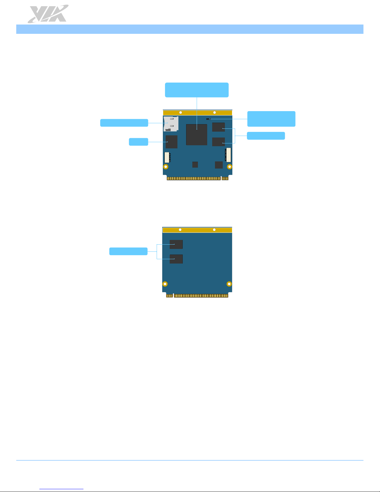
1.3. Layout Diagram
Micro SD card slot
eMMC
DDR3 SDRAM
NXP i.MX 6DualLite
Cortex A9 dual core SoC
Micro SD/SPI
boot select jumper
Figure 1: Layout diagram of the QSM-8Q60 (top side)
DDR3 SDRAM
Figure 2: Layout diagram of the QSM-8Q60 (bottom side)
Page 12
QSM-8Q60 User Manual
5
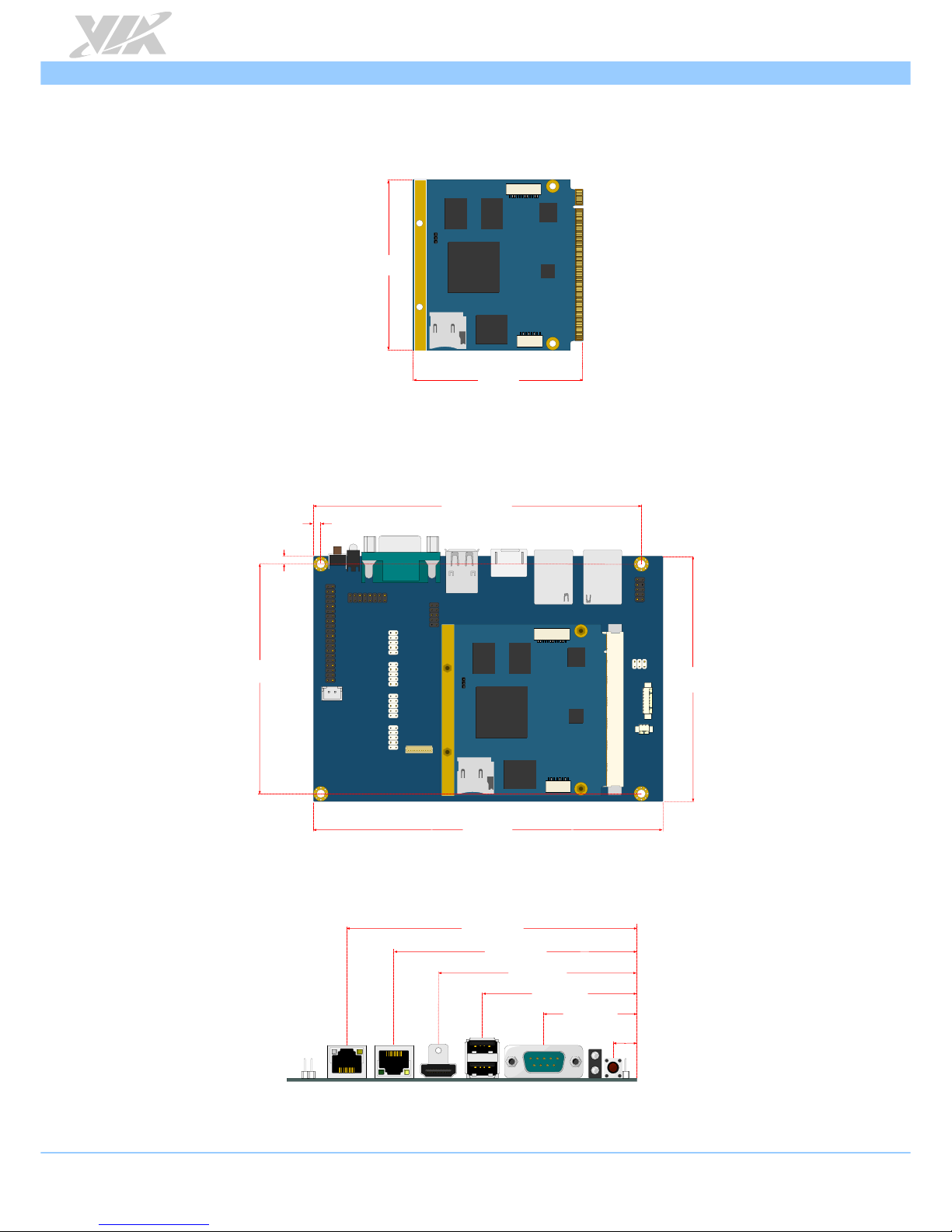
1.4. Product Dimensions
70mm
70mm
Figure 3: Dimensions of the QSM-8Q60 module (top view)
QSMDB2
137.19mm
95.24mm
3mm
102mm
3.68mm
146mm
Figure 4: Dimensions of the QSM-8Q60 attached to the carrier board (top view)
11.19mm
0.00
37.88mm
63.48mm
82.63mm
101.66mm
121.01mm
Figure 5: Dimensions of the QSMDB2 external I/O
Page 13
QSM-8Q60 User Manual
6
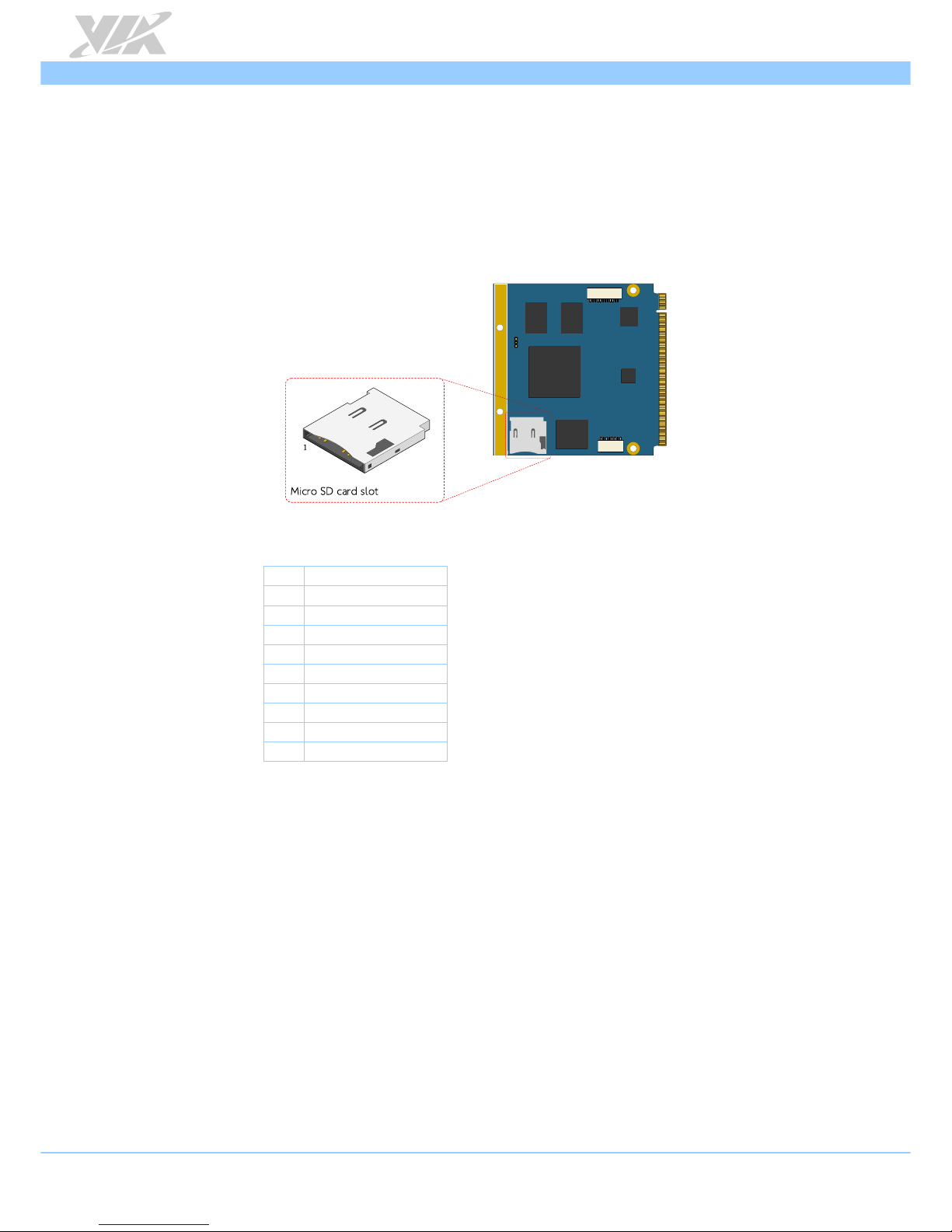
2. Onboard Slot
This chapter provides information about the QSM-8Q60’s onboard slot.
2.1. Micro SD Card Slot
The QSM-8Q60 module comes with a Micro SD card slot. The Micro SD card slot offers expandable
storage of Micro SD card memory up to 32GB capacity. The pinout of the Micro SD card slot is shown
below.
Figure 6: Micro SD card slot diagram
Pin Signal
1 SD0DATA2
2 SD0DATA3
3 SD0CMD
4 VDD (3.3V)
5 SD0CLK
6 GND
7 SD0DATA0
8 SD0DATA1
9 SD0_CD
Table 1: Micro SD card slot pinout
Page 14
QSM-8Q60 User Manual
7
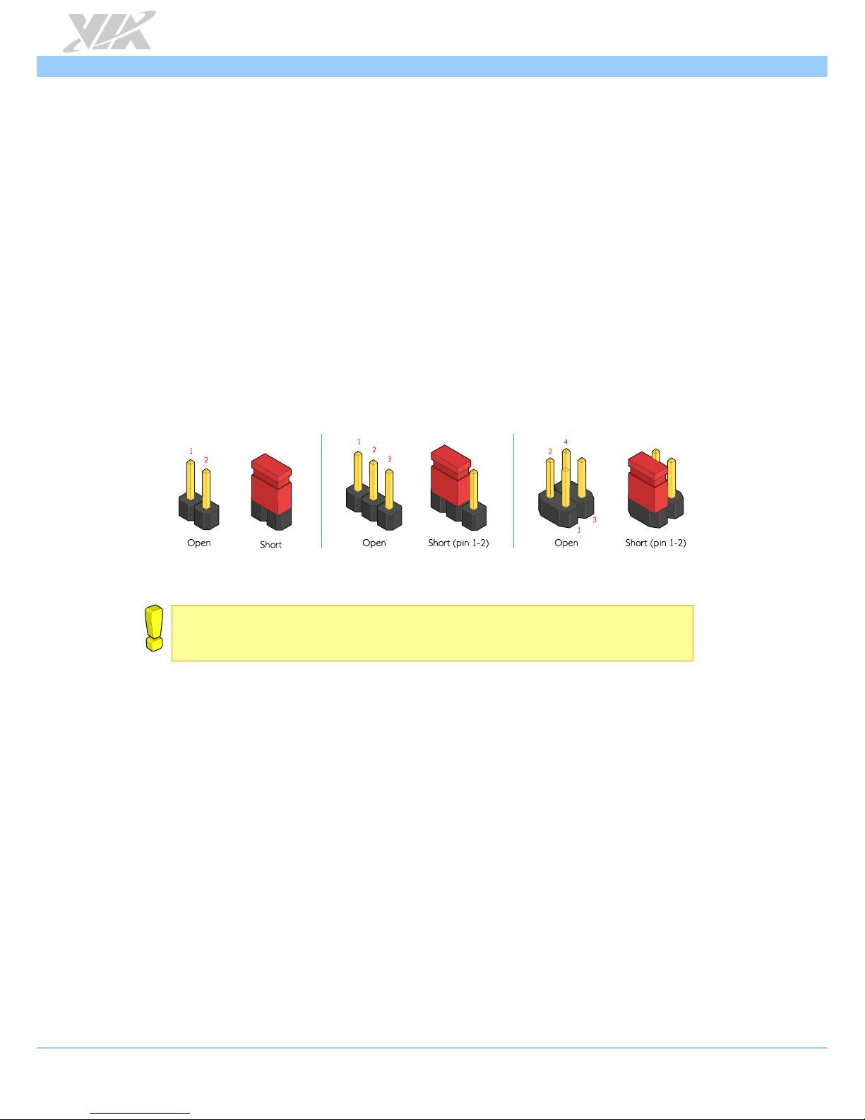
3. Onboard Jumpers
This section will explain how to configure the QSM-8Q60 to match the needs of your application by
setting the jumpers.
Jumper Description
A jumper consists of pair conductive pins used to close in or bypass an electronic circuit to set up or
configure particular feature using a jumper cap. The jumper cap is a small metal clip covered by plastic. It
performs like a connecting bridge to short (connect) the pair of pins. The usual colors of the jumper cap
are black/red/blue/white/yellow.
Basic Jumper Configuration
There are two settings of the jumper pin: “
Short
and
Open
”. The pins are “
Short
” when a jumper cap is
placed on the pair of pins. The pins are ”
Open
” if the jumper cap is removed.
In addition, there are jumpers that have three or more pins, and some pins are arranged in series. In case
of a jumper with three pins, place the jumper cap on pin 1 and pin 2 or pin 2 and 3 to
Short
it.
Some jumper size is small or mounted on the crowded location on the board that makes it difficult to
access. Therefore, using a long-nose pliers in installing and removing the jumper cap is very helpful.
Figure 7: Jumper settings example
Caution:
Make sure to install the jumper cap on the correct pins. Installing it in the wrong pin might cause damage and
malfunction.
Page 15

QSM-8Q60 User Manual
8
3.1. Micro SD/SPI Boot Select Jumper
The Micro SD/SPI boot select jumper labeled as “J11” is set to specify the boot device. The default setting
is the Micro SD. The jumper settings are shown below.
Figure 8: Micro SD/SPI boot select jumper diagram
Setting Pin 1 Pin 2 Pin 3
Micro SD (default) Short Short Open
SPI Open Short Short
Table 2: Micro SD/SPI boot select jumper settings
Page 16

QSM-8Q60 User Manual
9
4. Hardware Installation
This chapter provides information about hardware installation procedures.
4.1. Installing the QSM-8Q60 Module on the QSMDB2
Carrier Board
Step 1
Locate the mounting points and the Qseven MXM slot on the QSMDB2 carrier board.
Figure 9: Mounting points and Qseven MXM connector
Step 2
Install four 5mm hex spacers on the carrier board. From the bottom of the carrier board, tighten the hex
spacers by using the M2.5x4mm screws.
QSMDB2
Hex spacer
M2.5x4mm screw
Top side
Bottom side
QSMDB2 carrier board
Figure 10: Installing the hex spacers on the QSMDB2 carrier board
Page 17

QSM-8Q60 User Manual
10
Step 3
Align the notch on the QSM-8Q60 module with the protruding wedge on the Qseven™ MXM connector
then insert the module at 30° angle. Once the module has been inserted, push down the module until
the screw holes align with the hole of hex spacers.
Figure 11: Installing QSM-8Q60 module
Step 4
Secure the QSM-8Q60 module with four 7mm hex spacer screws.
Figure 12: Securing the QSM-8Q60 module
Page 18

QSM-8Q60 User Manual
11
Step 5
Install the heatsink on the QSM-8Q60 module.
QSMDB2
Figure 13: Installing the heatsink
Step 6
Secure the heatsink with M2.5x4mm screws.
QSMDB2
Heatsink
QSM-8Q60 module
QSMDB2 carrier board
M2.5x4mm screw
Figure 14: Securing the heatsink
Page 19

QSM-8Q60 User Manual
12
5. Software and Technical Supports
5.1. Linux Support
The VIA QSM-8Q60 module is highly compatible with Linux Kernel operating system.
• Linux Kernel 4.1.15 (QSM-8Q60-QP SKU)
• Linux Kernel 3.14.28 (QSM-8Q60 SKU)
5.1.1. Driver Installation
Linux Driver Support
Linux drivers are provided through various methods including:
• Drivers provided by VIA
• Using a driver built into a distribution package
• Visiting
www.viatech.com
for the latest updated drivers
• Installing a third party driver (such as the ALSA driver from the Advanced Linux Sound
Architecture project for integrated audio)
5.2. Technical Supports and Assistance
• For utilities downloads, latest documentation and new information about the QSM-8Q60, go to
http://www.viatech.com/en/boards/modules/qsm-8q60/
• For technical support and additional assistance, always contact your local sales representative or
board distributor, or go to
http://www.viatech.com/en/about/contact/
to fill up the form request.
• For OEM clients and system integrators developing a product for long term production, other
code and resources may also be made available. Contact VIA to submit a request.
Page 20

QSM-8Q60 User Manual
13
Appendix A. QSMDB2 Carrier Board
Reference
A.1. Board Specifications
Qseven™ Rev. 2.0 compliant
o Support QSM-8Q60 module
Audio
o NXP SGTL5000 low power stereo codec
Front Panel I/O
o 2 x USB 2.0 ports
o 1 x HDMI port
o 1 x COM port (TX/RX for debug)
o 1 x Gigabit Ethernet LAN port
o 1 x 10/100Mbps Ethernet port
o 1 x Power LED indicator
o 1 x Wi-Fi activity LED indicator
o 1 x Reset button
Onboard connectors and pin headers
o 1 x Qseven
™
MXM connector
o 1 x GPIO pin header (16 GPI + 16 GPO)
o 1 x CAN bus connector (supports two CAN bus)
o 4 x COM pin headers (RS-232/RS-422/RS-485)
o 1 x Serial and I
²
C pin header (supports two COM ports for TX/RX, and one I2C)
o 1 x Audio pin header (for Line-in, Line-out and Mic-in)
o 1 x Touch panel connector
o 1 x RTC battery connector
o 1 x DC-in connector
o 1 x Dual-channel 18/24-bit LVDS panel connector
o 1 x LVDS inverter connector
o 1 x miniPCIe slot
o 1 x SIM card slot
Onboard Jumper
o 1 x Backlight and Panel power select jumper
Power Supply
o 15V ~ 24V DC-in
Form Factor and Dimension
o 3.5” Form Factor 14.6cm x 10.2cm (5.75” x 4.01”)
Operating Temperature
o -20°C ~ 70°C
Operating Humidity
o 0% ~ 95% (non-condensing)
Page 21

QSM-8Q60 User Manual
14
A.2. QSMDB2 External I/O Connectors
The QSMDB2 carrier board has a wide selection of interfaces. It includes a selection of frequently used
ports as part of the external I/O coastline.
A.2.1. Front Panel I/O
COM 2
Reset button
Power LED
USB 2.0
Wi-Fi LEDHDMI
Gigabit Ethernet
10/100Mbps Ethernet
Figure 15: QSMDB2 front panel I/O
A.3. QSMDB2 Layout Diagram
QSMDB2
CAN bus
Audio
GPIO
DC-in
COM 7
COM 6
COM 4
COM 5
Serial and I C
2
RTC battery connector
Touch panel
Backlight and Panel
power select jumper
Qseven MXM
Figure 16: QSMDB2 layout label (top side)
O
L
O
MiniPCIe
SIM card slot
Figure 17: QSMDB2 layout label (bottom side)
Page 22

QSM-8Q60 User Manual
15
A.3.1. QSMDB2 Onboard Connectors, Slots and Pin Headers
A.3.1.1. Qseven MXM Connector
The Qseven MXM connector labeled as “J2” is an onboard connector for connecting the Qseven™
modules (e.g. QSM-8Q60 module) to the carrier board. The Qseven MXM connector is consists of 230pins. The pinout of the Qseven MXM connector is shown below.
QSMDB2
1
J
2
2
1
Figure 18: Qseven MXM connector diagram
Pin Signal Pin Signal
1 GND 2 GND
3 TXRXM_D 4 TXRXM_C
5 TXRXP_D 6 TXRXP_C
7 NC 8 NC
9 TXRXM_B 10 TXRXM_A
11 TXRXP_B 12 TXRXP_A
13 LED2_LINK- 14 LED1_ACT15 NC 16 GPIO_19_PLED
17 NC 18 USB_OTG_PWR_EN
19 NC 20 NC
21 NC 22 NC
23 GND 24 GND
25 GND 26 NC
27 NC 28 RESET_N
29 SATA0_TX+ 30 UART3_RX
31 SATA0_TX- 32 UART3_TX
33 SATA_ACT- 34 GND
35 SATA0_RX+ 36 UART3_-CTS
37 SATA0_RX- 38 UART3_-RTS
39 GND 40 GND
41 NC 42 SD1_CLK
43 SD1_CD- 44 SD1_LED
45 SD1_CMD 46 SD1_WP
47 SD1_PWR- 48 SD1_DATA1
49 SD1_DATA0 50 SD1_DATA3
51 SD1_DATA2 52 SD1_DATA5
53 SD1_DATA4 54 SD1_DATA7
55 SD1_DATA6 56 NC
Page 23

QSM-8Q60 User Manual
16
57 GND 58 GND
59 AUD4_TXFS 60 UART2_RX
61 GPIO_0_CLKO 62 UART2_TX
63 AUD4_TXC 64 NC
65 AUD4_TXD 66 I2C3_SCL
67 AUD4_RXD 68 I2C3_SDA
69 NC 70 NC
71 NC 72 WDOG_B
73 GND 74 GND
75 NC 76 NC
77 NC 78 NC
79 NC 80 USB_4_OC
81 NC 82 USBD_T483 NC 84 USBD_T4+
85 USB_2_3_OC 86 USB_0_OTG_OC
87 USBD_T3- 88 USBD_T289 USBD_T3+ 90 USBD_T2+
91 NC 92 USBD_OTG_ID
93 OTG_USBD_T1- 94 USBD_T095 OTG_USBD_T1+ 96 USBD_T0+
97 GND 98 GND
99 LVDS0_TX0_P 100 LVDS1_TX0_P
101 LVDS0_TX0_N 102 LVDS1_TX0_N
103 LVDS0_TX1_P 104 LVDS1_TX1_P
105 LVDS0_TX1_N 106 LVDS1_TX1_N
107 LVDS0_TX2_P 108 LVDS1_TX2_P
109 LVDS0_TX2_N 110 LVDS1_TX2_N
111 LVDS_PPEN 112 LVDS_BLEN
113 LVDS0_TX3_P 114 LVDS1_TX3_P
115 LVDS0_TX3_N 116 LVDS1_TX3_N
117 GND 118 GND
119 LVDS0_CLK_P 120 LVDS1_CLK_P
121 LVDS0_CLK_N 122 LVDS1_CLK_N
123 LVDS_PWM2 124 NC
125 I2C1_SDA 126 USB_0_2_3_4_EN
127 I2C1_SCL 128 HDMI_CEC_IN
129 CAN_TX1 130 CAN_RX1
131 HDMI_CLKP 132 TP_2
133 HDMI_CLKM 134 TP_3
135 GND 136 GND
137 HDMI_D1P 138 NC
139 HDMI_D1M 140 NC
141 GND 142 GND
143 HDMI_D0P 144 NC
145 HDMI_D0M 146 NC
147 GND 148 GND
149 HDMI_D2P 150 I2C2_SDA
151 HDMI_D2M 152 I2C2_SCL
153 HDMI_HPD 154 GND
155 PCIe_CREFCLKP 156 PCIE_WAKE_B
157 PCIe_CREFCLKM 158 PCIE_RST_B
159 GND 160 GND
161 NC 162 NC
Page 24

QSM-8Q60 User Manual
17
163 NC 164 NC
165 GND 166 GND
167 NC 168 NC
169 NC 170 NC
171 UART1_TX 172 UART1_-RTS
173 NC 174 CAN_TX2
175 NC 176 CAN_RX2
177 UART1_RX 178 UART1_CTS
179 PCIe_CTXP 180 PCIe_CRXP
181 PCIe_CTXM 182 PCIe_CRXM
183 GND 184 GND
185 GPIO6_IO11 186 GPIO_7
187 GPIO_2 188 GPIO_8
189 GPIO6_IO14 190 GPIO6_IO7
191 GPIO_5 192 GPIO6_IO16
193 VDD_RTC_IN 194 NC
195 NC 196 PWM_OUT1
197 GND 198 GND
199 CSPI3_MOSI 200 CSPI3_CS0
201 CSPI3_MISO 202 CSPI3_CS1
203 CSPI3_CLK 204 NC
205 NC 206 NC
207 NC 208 NC
209 NC 210 NC
211 5VIN 212 NC
213 5VIN 214 5VIN
215 5VIN 216 5VIN
217 5VIN 218 5VIN
219 5VIN 220 5VIN
221 5VIN 222 5VIN
223 5VIN 224 5VIN
225 5VIN 226 5VIN
227 5VIN 228 5VIN
229 5VIN 230 5VIN
Table 3: Qseven MXM connector pinout
Page 25

QSM-8Q60 User Manual
18
A.3.1.2. Audio Pin Header
The QSMDB2 carrier board has an Audio pin header for Line-in, Line-out and and Mic-in. The pin header is
labeled as “AUDIO1”. The pinout of the Audio pin header is shown below.
QSMDB2
1
AUDIO1: Audio pin header
1
Figure 19: Audio pin header diagram
Pin Signal Pin Signal
1 HEAD_RIGHT 2 HEAD_LEFT
3 LINE_IN_R 4 LINE_IN_L
5 MIC_IN 6 MIC_IN
7 — 8 NC
9 GND_ANALOG 10 GND_ANALOG
Table 4: Audio pin header pinout
A.3.1.3. Touch Panel Connector
The Touch panel connector labeled as “TOUCH_C1” is used to connect the touch sensor controller for 5wire/4-wire touch panel. The pinout of the touch panel connector is shown below.
QSMDB2
1
TOUCH_C1: Touch Panel connector
1
Figure 20: Touch panel connector diagram
Pin Signal
1 GND
2 I2C1_SDA
3
I2C1_SCL
4
5VIN
5 GPIO_2
6 GPIO6_IO11
7 3P3V
Table 5: Touch panel connector pinout
Page 26

QSM-8Q60 User Manual
19
A.3.1.4. RTC Battery Connector
The QSMDB2 carrier board is equipped with onboard RTC battery connector used for connecting the
external cable battery that provides power to the 32.768 KHz crystal oscillator for Real Time Clock (RTC).
The RTC battery connector is labeled as “J3”. The connector pinout is shown below.
QSMDB2
1
!"# $%& '())*+, -.//*-).+
0
Figure 21: RTC battery connector diagram
Pin Signal
1 VDD_RTC
2
GND
Table 6: RTC battery connector pinout
A.3.1.5. DC-In Connector
The QSMDB2 carrier board supports DC-in connector to provide power to the system. The 2-pin DC-in
connector is used to connect the DC-in power jack. The connector is labeled as “J6”. The pinout of the
DC-in connector is shown below.
QSMDB2
1
345 D6789 :;99<:=;>
?
Figure 22: DC-in connector diagram
Pin Signal
1 DCIN
2 GND
Table 7: DC-in connector pinout
Page 27

QSM-8Q60 User Manual
20
A.3.1.6. COM Pin headers
The QSMDB2 carrier board is equipped with four COM pin headers labeled as “COM4, COM5, COM6
and COM7” that supports RS-232/RS-422/RS-485 mode. The pinouts of COM pin headers are shown
below.
QSMDB2
1
C@ABE C
OM 4 pin header
F
C@AGE C
OM 5 pin header
H
H
H
H
F
C@AIE C
OM 6 pin header
F
C@AKE C
OM 7 pin header
Figure 23: COM4, COM 5, COM 6 and COM 7 pin header diagram
Pin Signal Pin Signal
1 IC_DCD1 2 IC_RXD1
3 IC_TXD1 4 IC_DTR1
5 GND 6 IC_DSR1
7 IC_RTS1 8 IC_CTS1
9 COM_RI1 10 —
Table 8: COM pin header pinout
Page 28

QSM-8Q60 User Manual
21
A.3.1.7. Serial and I
2
C Pin Header
The QSMDB2 carrier board is equipped with Serial and I2C pin header labeled as “COM1_3”. The Serial
and I2C pin header can support two COM ports (COM 1 and COM 3) used for TX/RX only, and one I2C
device. The pinout of Serial and I2C pin header is shown below.
QSMDB2
1
1
MNPQRST
Serial and I C pin header
2
Figure 24: Serial and I2C pin header diagram
Pin Signal Pin Signal
1 COM_TXD1 2 COM_TXD3
3 COM_RXD1 4 COM_RXD3
5 GND 6 GND
7 GND 8 I2C3_SDA
9 — 10 I2C3_SCL
Table 9: Serial and I2C pin header pinout
Page 29

QSM-8Q60 User Manual
22
A.3.1.8. CAN Bus Connector
The QSMDB2 carrier board provides CAN bus connector that support CAN protocol specification Version
2.0B. The onboard CAN bus connector labeled as “CANBUS” supports two CAN bus ports. The pinout of
the CAN bus connector is shown below.
Figure 25: CAN bus connector diagram
Pin Signal
1
NC
2 NC
3 NC
4 CANH1
5 NC
6 GND
7 CANL2
8 CANH2
9 GND
10 CANL1
Table 10: CAN bus connector pinout
Page 30

QSM-8Q60 User Manual
23
A.3.1.9. GPIO Pin Header
The QSMDB2 carrier board provides GPIO pin header labeled as “GPIO”. The 32 digital inputs and
outputs can be programmed to read or control devices, with input or output defined. The GPIO pin
header supports up to 16 GPI and 16 GPO signals. The pinout of the GPIO pin header is shown below.
Figure 26: GPIO pin header diagram
Pin Signal Pin Signal
1 GPIO0 2 GPIO4
3 GPIO1 4 GPIO5
5 GPIO2 6 GPIO6
7 GPIO3 8 GPIO7
9 GND 10 GND
11 GPIO10 12 GPIO14
13 GPIO11 14 GPIO15
15 GPIO12 16 GPIO16
17 GPIO13 18 GPIO17
19 GND 20 —
21 GPIO20 22 GPIO24
23 GPIO21 24 GPIO25
25 GPIO22 26 GPIO26
27 GPIO23 28 GPIO27
29 GND 30 GND
31 GPIO30 32 GPIO34
33 GPIO31 34 GPIO35
35 GPIO32 36 GPIO36
37 GPIO33 38 GPIO37
39 GND 40 GND
Table 11: GPIO pin header pinout
Page 31

QSM-8Q60 User Manual
24
A.3.1.10. LVDS Panel Connector
The QSMDB2 carrier board supports an onboard 40-pin LVDS connector used for connecting the panel’s
LVDS cable directly to support LVDS panel without any need of a daughter card. The connector is
labeled as “LVDS1”. The pinout of the LVDS connector is shown below.
U
V
W
X
Y
U
Z
[
LVDS1: LVDS panel connector
1
1
1
Figure 27: LVDS panel connector diagram
Pin Signal Pin Signal
1 LVDS1_TX0_NC 2 PVDD
3 LVDS1_TX0_PC 4 PVDD
5 GND 6 GND
7 LVDS1_TX1_NC 8 GND
9 LVDS1_TX1_PC 10 LVDS0_TX0_NC
11 GND 12 LVDS0_TX0_PC
13 LVDS1_TX2_NC 14 GND
15 LVDS1_TX2_PC 16 LVDS0_TX1_NC
17 GND 18 LVDS0_TX1_PC
19 LVDS1_CLK_NC 20 GND
21 LVDS1_CLK_PC 22 LVDS0_TX2_NC
23 GND 24 LVDS0_TX2_PC
25 LVDS1_TX3_NC 26 GND
27 LVDS1_TX3_PC 28 LVDS0_CLK_NC
29 GND 30 LVDS0_CLK_PC
31 5VIN 32 GND
33 3P3V 34 LVDS0_TX3_NC
35 NC 36 LVDS0_TX3_PC
37 NC 38 LVDS0_EDID_SCL
39 NC 40 LVDS0_EDID_SDA
Table 12: LVDS panel connector pinout
Page 32

QSM-8Q60 User Manual
25
A.3.1.11. LVDS Inverter Connector
The QSMDB2 carrier board provides LVDS inverter connector located on the bottom side of the board for
supplying power to the backlight of the LCD panel. The connector is labeled as “INVERTER1”. The pinout
of the LVDS inverter connector is shown below.
\
]
^
_
`
\
a
b
c
defghighjk dlmnopno qrllnqpro
j
c
Figure 28: LVDS inverter connector diagram
Pin Signal
1 IVDD
2 IVDD
3 LVDS_EN
4 DISP0_CONTRAST
5 LVDS_EN
6 DISP0_CONTRAST
7 GND
8 GND
Table 13: LVDS inverter connector pinout
Page 33

QSM-8Q60 User Manual
26
A.3.1.12. MiniPCIe Slot
The QSMDB2 carrier board is equipped with miniPCIe slot labeled as “MINIPCIE1”. The miniPCIe slot is
for 3G module to provide a 3G function. The pinout of the MiniPCIe slot is shown below.
s
t
u
v
w
s
x
y
2
1
52
51
z{|{}~{ z}~{
e slot
Figure 29: MiniPCIe slot diagram
Pin Signal Pin Signal
1 PCIE_WAKE_B 2 MPCIE_3V3
3 NC 4 GND
5 NC 6 DDR_1_5V
7 NC 8 USIM_VCC
9 GND 10 USIM_DATA
11 PCIe_CREFCLKM 12 USIM_CLK
13 PCIe_CREFCLKP 14 USIM_RST
15 GND 16 USIM_VCC
17 NC 18 GND
19 NC 20 NC
21 GND 22 PCIE_RST_B
23 PCIe_CRXM 24 MPCIE_3V3
25 PCIe_CRXP 26 GND
27 GND 28 DDR_1_5V
29 GND 30 PCIe_SMB_CLK
31 PCIe_CTXM 32 PCIe_SMB_DATA
33 PCIe_CTXP 34 GND
35 GND 36 PCIE_USB_DM
37 GND 38 PCIE_USB_DP
39 MPCIE_3V3 40 GND
41 MPCIE_3V3 42 LED_WWAN_B
43 GND 44 LED_WLAN_B
45 NC 46 LED_WPAN_B
47 NC 48 DDR_1_5V
49 NC 50 GND
51 NC 52 MPCIE_3V3
Table 14: MiniPCIe slot pinout
Page 34

QSM-8Q60 User Manual
27
A.3.1.13. SIM Card Slot
The QSMDB2 carrier board is equipped with SIM card slot located on the bottom side of the board which
can supports a 3G SIM card. Using the SIM card slot on QSMDB2 requires a 3G module installed in the
MiniPCIe slot to enable the 3G function, otherwise the SIM card slot is disabled. The SIM card slot is
labeled as “SIM1”. The pinout of the SIM card slot is shown below.
1
1
Figure 30: SIM card slot diagram
Pin Signal
1 USIM_DATA
2 USIM_CLK
3 USIM_VCC
4 USIM_RST
5 GND
6 USIM_VCC
Table 15: SIM card slot pinout
Page 35

QSM-8Q60 User Manual
28
A.3.2. QSMDB2 Onboard Jumpers
A.3.2.1. Backlight and Panel Power Select Jumper
The power selectors for backlight and panel are controlled by the jumper labeled as “J1”. It can select
either +12V or +5V for backlight power and +3.3V or +5V for panel power. The jumper settings are
shown below.
QSMDB2
2
1
4
6
3
5
¡¢£¤
+5V
Backlight power select settings
+3.3V (default)
+5V
Panel power select settings
J1: Backlight and Panel
power select jumper
1 1
1 1
1
Figure 31: Backlight and Panel power select jumper diagram
Setting Pin 1 Pin 3 Pin 5
+12V (default) Short Short Open
+5V Open Short Short
Table 16: Backlight power select jumper settings
Setting Pin 2 Pin 4 Pin 6
+3.3V (default) Short Short Open
+5V Open Short Short
Table 17: Panel power select jumper settings
Page 36

QSM-8Q60 User Manual
29
Appendix B. Installing Wireless Accessories
This section provides information on how to install the optional wireless accessories to provide wireless
connection such as Wi-Fi, Bluetooth, GPS and 3G.
B.1. Inserting VNT9271 USB Wi-Fi Dongle
Step 1
Locate a USB 2.0 port on the front panel I/O of the QSMDB2 carrier board.
Step 2
Insert the VNT9271 dongle in one of the USB 2.0 port.
Figure 32: Inserting VNT9271 USB Wi-Fi dongle
Page 37

QSM-8Q60 User Manual
30
B.2. Installing EMIO-1541 miniPCIe Wi-Fi Module
Step 1
Locate the miniPCIe slot and install the hex standoff screw to the QSMDB2 carrier board.
Carrier Board (Q
SMDB2)
Figure 33: Installing hex standoff screw for EMIO-1541 module
Step 2
Align the notch on the EMIO-1541 module with the protruding wedge on the miniPCIe slot then insert the
module at 30° angle.
Carrier Board (Q
SMDB2)
30
Figure 34: Installing EMIO-1541 module
Step 3
Once the module has been inserted, push down the module until the screw hole align with the mounting
hole on the hex standoff. Secure the module with screw to the standoff.
Carrier Board (Q
SMDB2)
Figure 35: Securing EMIO-1541 module
Page 38

QSM-8Q60 User Manual
31
Step 4
Insert the Wi-Fi antenna cable into the antenna hole from inside of the chassis. Insert the washer, and
fasten it with the nut. Then install the external antenna.
SS
1
2
3
4
P
a
nel
I/O pl
a
te
Figure 36: Installing Wi-Fi antenna of EMIO-1541 module
Step 5
Connect the other end of the Wi-Fi antenna cable onto the micro-RF connector labeled “TRX” on the
EMIO-1541 module.
Carrier Board (QSMDB2)
Figure 37: Connecting Wi-Fi antenna cable to the EMIO-1541 module
Page 39

QSM-8Q60 User Manual
32
B.3. Installing EMIO-2531 miniPCIe Wi-Fi + Bluetooth
Module
Step 1
Take off the screw and nut on the EMIO-2531 as shown in the illustration.
Figure 38: Removing screw on the EMIO-2531 module
Step 2
Align the notch on the EMIO-2531 module with the protruding wedge on the miniPCIe slot then insert the
module at 30° angle.
Carrier Board (Q
SMDB2)
30
Figure 39: Installing EMIO-2531 module
Step 3
Once the module has been inserted, push down the module until the screw hole align with the mounting
hole on the standoff. Reinstall the screw to secure the module to the standoff.
Carrier Board (Q
SMDB2)
Figure 40: Securing EMIO-2531 module
Page 40

QSM-8Q60 User Manual
33
Step 4
Insert the Wi-Fi antenna cable into the antenna hole from inside of the chassis. Insert the washer, fasten it
with the nut and install the external antenna.
SS
1
2
3
4
P
a
nel
I/O p
l
a
te
Figure 41: Installing Wi-Fi antenna of EMIO-2531 module
Step 5
Gently connect the other end of the Wi-Fi antenna cable to the micro-RF connector labeled “MH2” on the
EMIO-2531 module.
Carrier Board (Q
SMDB2)
Figure 42: Connecting Wi-Fi antenna cable to the EMIO-2531 module
Page 41

QSM-8Q60 User Manual
34
B.4. Installing EMIO-2550 miniPCIe Mobile Broadband
Module
Step 1
Insert the SIM card on the bottom side of the EMIO-2550 module. (EMIO-2550-00A1)
Step 2
Connect first the other end of the GPS antenna cable to the micro-RF connector labeled “GPS” on the
bottom side of EMIO-2550 module. Insert the 3G and GPS antenna cables into the antenna holes from
inside of the chassis then insert their respective washers, and fasten it with the nut.
Panel I/O plate
1
2
3
Figure 43: Connecting GPS antenna cable to the EMIO-2550 module
Step 3
Align the notch on the EMIO-2550 module with the protruding wedge on the miniPCIe slot then insert the
module at 30° angle.
Carrier Board (Q
SMDB2)
Figure 44: Installing EMIO-2550 module
Page 42

QSM-8Q60 User Manual
35
Step 4
Once the module has been inserted, push down the module until the screw hole align with the mounting
hole on the standoff. Secure the module with the screw to the standoff.
Carrier Board (Q
SMDB2)
Figure 45: Securing EMIO-2550 module
Step 5
Connect the other end of the 3G antenna cable onto the micro-RF connector labeled “MAN” on the
EMIO-2550 module.
Carrier Board (Q
SMDB2)
Carrier Board (Q
SMDB2)
Figure 46: Connecting 3G antenna cable to the EMIO-2550 module
Page 43

QSM-8Q60 User Manual
36
Step 6
Install the 3G and GPS external antennas respectively.
Carrier Board (Q
SMDB2)
Figure 47: Installing 3G and GPS antenna of EMIO-2550 module
Page 44

QSM-8Q60 User Manual
37
Appendix C. Inserting SIM Card
This section provides information on how to insert the SIM card on the QSMDB2 carrier board.
Step 1
Push back firmly the SIM card slot to unlock the opening.
Step 2
Pull up the slot and place the SIM card inside the slot. Ensure the angled corner of the SIM card is placed
in the correct way before closing the slot.
Step 3
Gently close the slot by pulling down the SIM slot.
Step 4
Lock the SIM slot by sliding back the slot.
Carrier Board (QSMDB2)
1 2 3 4
Figure 48: Inserting SIM card on QSMDB2 carrier board
Page 45

 Loading...