

Page 1

User’s Manual
NAB-7400
Version 1.11
April 2, 2007
Page 2

Copyright
Copyright © 2006-2007 VIA Technologies Incorporated. All rights reserved.
No part of this document may be reproduced, transmitted, transcribed, stored in a retrieval
system, or translated into any language, in any form or by any means, electronic, mechanical,
magnetic, optical, chemical, manual or otherwise without the prior written permission of VIA
Technologies, Incorporated.
Trademarks
All trademarks are the property of their respective holders. PS/2 is a registered trademark of
IBM Corporation. Award BIOS is a registered trademark of Phoenix Technologies Ltd.
Macrovision
Apparatus Claims of U.S. Patent Nos. 4,631,603; 4,819,098; 4,907,093; 5,315,448; 6,516,132
licensed for limited viewing uses only. This product incorporates copyright protection
technology that is protected by certain U.S. patents and other intellectual property rights owned
by Macrovision and other rights owners. Use of this copyright protection technology must be
authorized by Macrovision, and is intended for home and other limited viewing uses only
unless otherwise authorized by Macrovision. Reverse engineering or disassembly is
prohibited.
Disclaimer
No license is granted, implied or otherwise, under any patent or patent rights of VIA
Technologies. VIA Technologies makes no warranties, implied or otherwise, in regard to this
document and to the products described in this document. The information provided in this
document is believed to be accurate and reliable as of the publication date of this document.
However, VIA Technologies assumes no responsibility for the use or misuse of the information
in this document and for any patent infringements that may arise from the use of this
document. The information and product specifications within this document are subject to
change at any time, without notice and without obligation to notify any person of such change.
Page 3

FCC-B Radio Frequency Interference Statement
This equipment has been tested and found to comply with the limits for a class B digital
device, pursuant to part 15 of the FCC rules. These limits are designed to provide reasonable
protection against harmful interference when the equipment is operated in a commercial
environment. This equipment generates, uses and can radiate radio frequency energy and, if not
installed and used in accordance with the instruction manual, may cause harmful interference
to radio communications. Operation of this equipment in a residential area is likely to cause
harmful interference, in which case the user will be required to correct the interference at his
personal expense.
Notice 1
The changes or modifications not expressly approved by the party responsible for compliance
could void the user's authority to operate the equipment.
Notice 2
Shielded interface cables and A.C. power cord, if any, must be used in order to comply with
the emission limits.
Tested To Comply
With FCC Standards
FOR HOME OR OFFICE USE
Page 4

Safety Instructions
1. Always read the safety instructions carefully.
2. Keep this User's Manual for future reference.
3. Keep this equipment away from humidity.
4. Lay this equipment on a reliable flat surface before setting it up.
5. The openings on the enclosure are for air convection hence protects the equipment from
overheating. DO NOT COVER THE OPENINGS.
6. Make sure the voltage of the power source and adjust properly 110/220V before
connecting the equipment to the power inlet.
7. Place the power cord in such a way that people cannot step on it. Do not place anything
over the power cord.
8. Always unplug the power cord before inserting any add-on card or module.
9. All cautions and warnings on the equipment should be noted.
10. Never pour any liquid into the opening. Liquid can cause damage or electrical shock.
11. If any of the following situations arises, get the equipment checked by a service personnel:
• The power cord or plug is damaged
• Liquid has penetrated into the equipment
• The equipment has been exposed to moisture
• The equipment has not work well or you cannot get it work according to User's
Manual.
• The equipment has dropped and damaged
• If the equipment has obvious sign of breakage
12. DO NOT LEAVE THIS EQUIPMENT IN AN ENVIRONMENT UNCONDITIONED,
STORAGE TEMPERATURE ABOVE 60 C (140F), IT MAY DAMAGE THE
EQUIPMENT.
CAUTION: Explosion or serious damage may occur if the battery is
incorrectly replaced. Replace only with the same or equivalent
battery type recommended by the manufacturer.
Page 5

TABLE OF CONTENTS
Table of Contents .................................................................. i
Chapter 1 ............................................................................ 1
Specifications .................................................................... 1
Mainboard Specifications..................................................... 2
Mainboard Layout............................................................... 4
Back Panel Layout.............................................................. 5
Chapter 2 ............................................................................ 6
Installation........................................................................ 6
CPU ................................................................................. 7
Memory Module Installation................................................. 9
Connecting the Power Supply..............................................10
Back Panel Ports ...............................................................11
Connectors.......................................................................12
Jumpers........................................................................... 18
Slots ............................................................................... 20
Chapter 3 ........................................................................... 21
BIOS Setup ...................................................................... 21
Entering Setup..................................................................22
Control Keys ..................................................................... 23
Navigating the BIOS Menus ................................................ 24
Getting Help .....................................................................25
Main Menu .......................................................................26
Standard CMOS Features.................................................... 28
IDE Drives .......................................................................29
Advanced BIOS Features .................................................... 30
CPU Feature..................................................................... 33
Hard Disk Boot Priority....................................................... 35
Advanced Chipset Features................................................. 36
AGP & P2P Bridge Control...................................................38
CPU & PCI Bus Control.......................................................40
Integrated Peripherals ....................................................... 41
Power Management Setup ..................................................44
Peripheral Activities ...........................................................46
IRQs Activities.................................................................. 48
i
Page 6

PNP/PCI Configurations ......................................................49
Frequency / Voltage Control ............................................... 51
Load Fail-Safe Defaults ...................................................... 53
Load Optimized Defaults..................................................... 54
Set Supervisor / User Password...........................................55
Save & Exit Setup ............................................................. 57
Exit Without Saving........................................................... 58
Chapter 4 ........................................................................... 59
Driver Installation ............................................................. 59
Driver Utilities .................................................................. 60
CD Content ......................................................................62
Appendix ............................................................................ 63
Watchdog Timer Configuration ............................................63
Sample Code .................................................................... 64
ii
Page 7

This page is left intentionally blank.
iii
Page 8

Page 9

HAPTER
C
1
Specifications
The ultra-compact and highly integrated VIA NAB-7400 uses the
mainboard form-factor developed by VIA Technologies, Inc. as
part of the company’s open industry-wide Total Connectivity
initiative. The mainboard enables the creation of an exciting new
generation of small, ergonomic, innovative and affordable
systems. Through a high level of integration, it occupies 66% of
the size of FlexATX mainboard form factor.
1
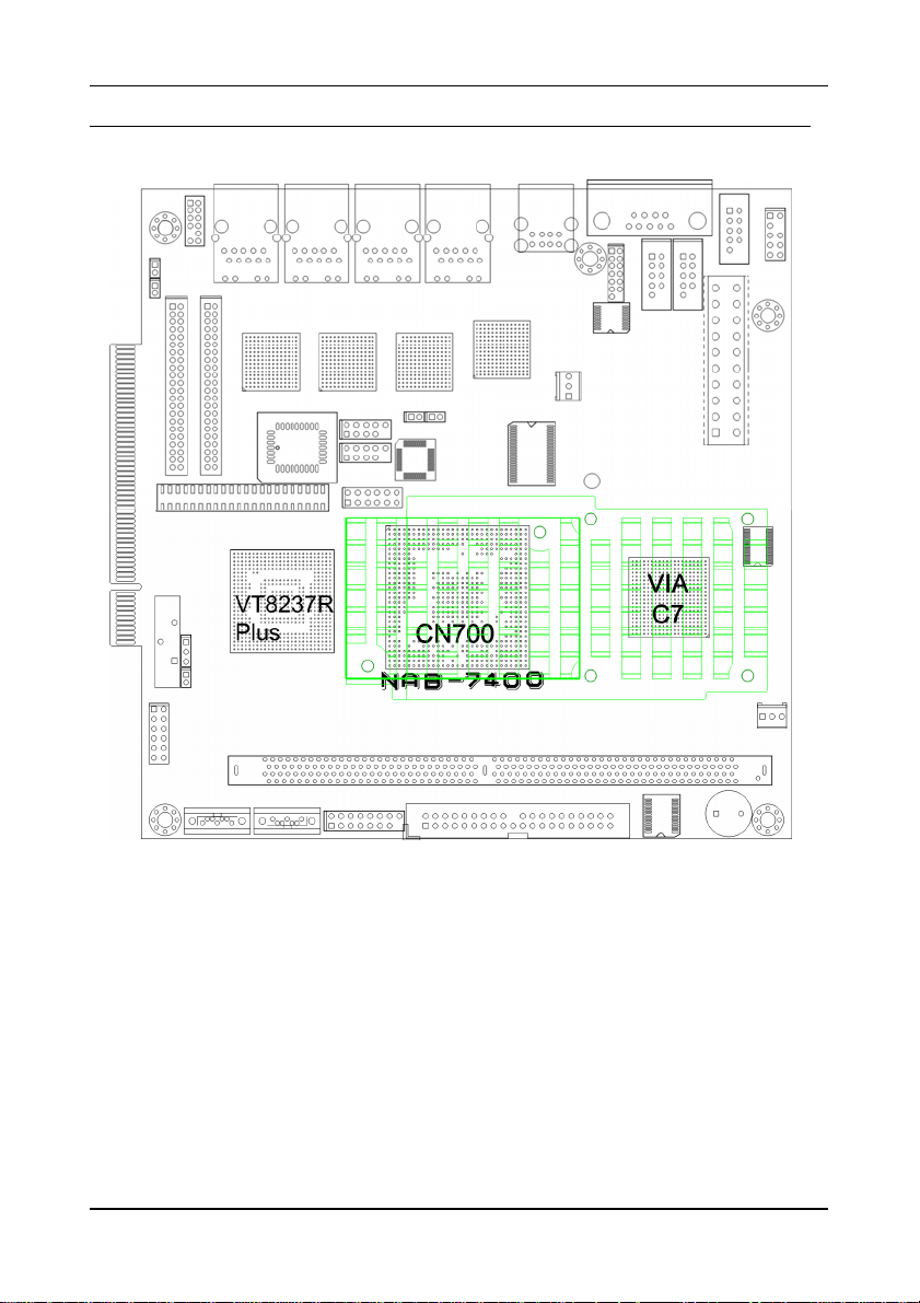
Page 10

Chapter 1
MAINBOAR D SPECIFICATIONS
CPU
• Support VIA C7 1.0GHz NanoBGA2 Processor
Chipset
• VIA CN700 North Bridge
• VIA VT8237R-Series South Bridge
Graphics
• Integrated UniChrome™ Pro 3D/2D AGP with MPEG-2 Video
Decoding Acceleration
Memory
• 1 x DDR2 533/400 DIMM slot (up to 1 GB)
Expansion Interface
• 2 x Mini PCI Interface
• 1 x 32-bit PCI Golden Finger
IDE
• 2 x UltraDMA 133/100/66 connectors (1 x 40 pins and 1 x 44
pins)
LAN
• 4 x Intel 82551ER Fast Ethernet PCI Controller or 4 x Intel
82541GI of Gigabit Ethernet Controllers
Back Panel I/O Ports
• 1 x COM port
• 2 x USB 2.0 ports
• 4 x RJ-45 LAN ports
2
Page 11

Onboard I/O Connectors
• 1 x VGA pin connector
• 1 x Digital I/O pin connector
• 1 x PS/2 pin connector for keyboard and mouse
• 1 x PCI pin header for storage module board
• 1 x PCI extension pin connector (for BXB board)
• 1 x Front panel pin connector
• 1 x Front panel LED pin connector for the LAN activity indicators
of Ethernet and wireless
• 2 x Fan pin connectors (CPU Fan and System Fan)
• 2 x SATA connectors
• 3 x USB pin connectors for 6 additional USB 2.0 ports (1 port
for VNT wireless board)
• 3 x Serial port pin connectors for COM2/3/4
• 1 x ATX Power connector
• 1 x Buzzer
BIOS
• Award BIOS with LPC 4/8Mbit flash memory capacity
Form Factor
• 6-layer PCB
• 17cm X 17.8cm
Specifications
3
Page 12
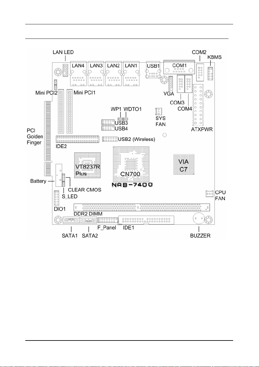
Chapter 1
MAINBOAR D LAYOUT
4
Page 13
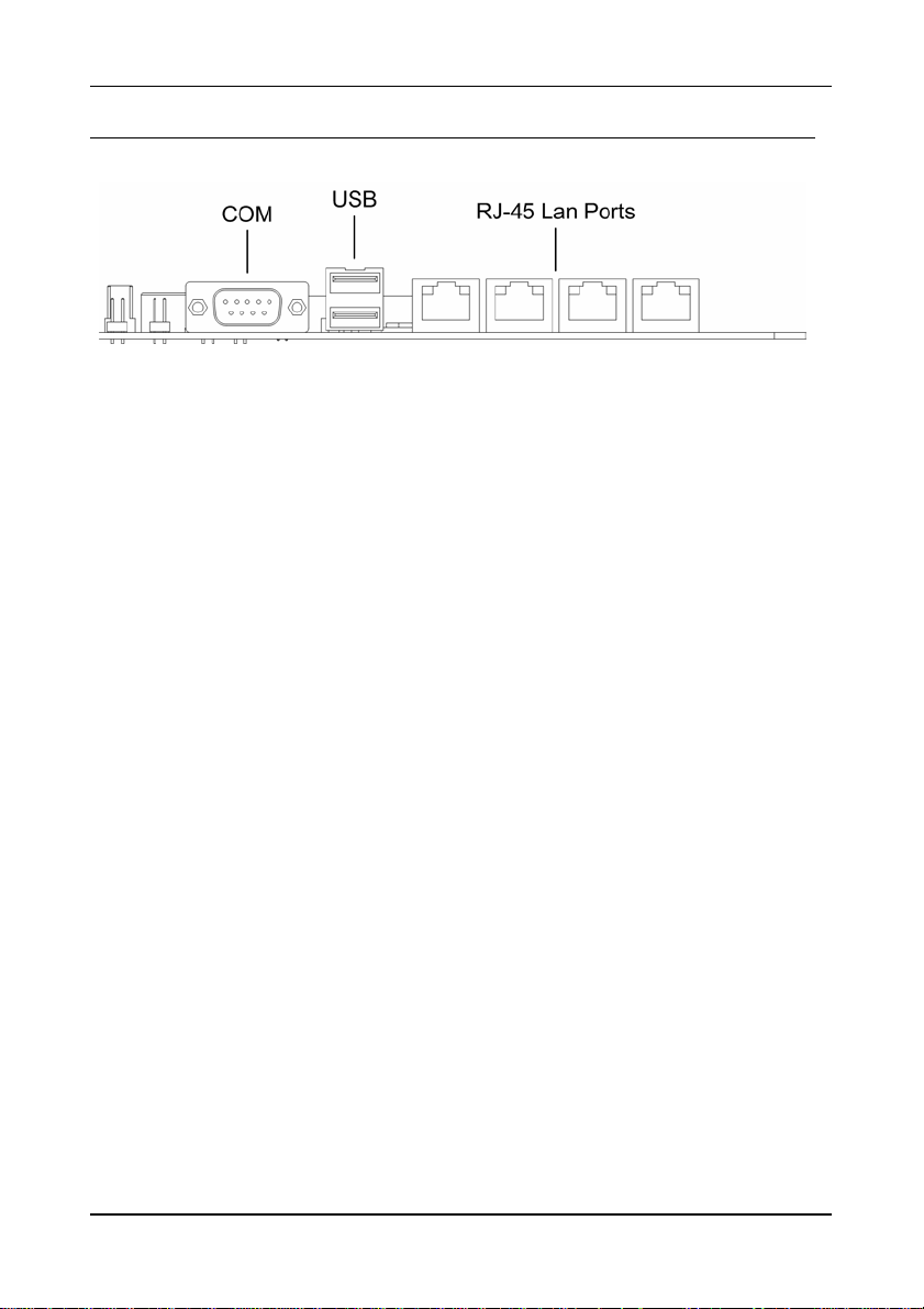
BACK PANEL LAYOUT
Specifications
5
Page 14

HAPTER
C
2
Installation
This chapter provides you with information about hardware
installation procedures. It is recommended to use a grounded wrist
strap before handling computer components. Electrostatic discharge
(ESD) can damage some components.
6
Page 15
Installation
CPU
The VIA NAB-7400 mainboard can support VIA C7 NanoBGA2 P rocessor.
7
Page 16

Chapter 2
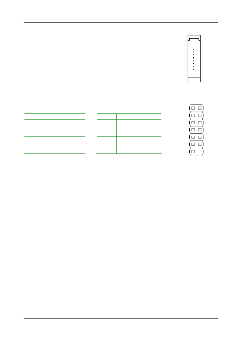
CPU Fan and System Fan: CPUFAN and SYSFAN
The CPUFAN (CPU fan) and SYSFAN (system fan) run on +12V and maintain
system cooling. When connecting the wire to the connectors, always be
aware that the red wire is the Positive and should be connected to the +12V .
The black wire is Ground and should always be connected to GND.
FAN_MCM is a switch that is used by high-quality fans to monitor the system
temperature and will automatically adjust according to the env ironment.
CPUFAN
Pin Signal
1 FAN_MCM
2 +12V
3 GND
SYSFAN
Pin Signal
1 FAN Speed detect
2 FAN_Control
3 GND
CPUFAN
1
SYSFAN
1
8
Page 17

Installation
MEMORY MODULE INSTALLATION
The VIA NAB-7400 mainboard provides one 240-pin DIMM slot for DDR2
400/533 SDRAM memory modules and supports th e memory size up to 1GB.
DIMM
DDR2 SDRAM Module Installation Procedures
• Locate the DIMM slot in the motherboard.
• Unlock a DIMM slot by pressing the retain ing clips ou tward.
• Align a DIMM on the socket such that the notch on the DIMM
matches the break on the slot.
• Firmly insert the DIMM into the slot until the retaining clips snap
back in place and the DIMM is properly seated.
Available DDR2 SDRAM Configurations
Refer to the table below for availab le DDR2 SDRAM configurations on the
mainboard.
Slot Module Size Total
DIMM 64MB, 128MB, 256MB, 512MB, 1GB 64MB-1GB
Maximum supported system memory 64MB-1GB
9
Page 18

Chapter 2
CONNECTING THE POWER SUPPLY
The VIA NAB-7400 mainboard supports a conventional ATX power supply for
the power system. Before inserting the power supply connector, always
make sure that all components are installed correctly to ensure that no
damage will be caused.
ATX 20-Pin Power Connector
To connect the ATX power supp ly, make sure the power plug is inserted in
the proper orientation and the pins are aligned. Then push down the plug
firmly into the connector.
Pin Signal
1 +3.3V
2 +3.3V
3 GND
4 +5V
5 GND
6 +5V
7 GND
8 Power Good
9 +5V Standby
10 +12V
11 +3.3V
12 -12V
13 GND
14 Power Supply On
15 GND
16 GND
17 GND
18 -5V
19 +5V
20 +5V
ATXPWR
11
20
1
10
10
Page 19
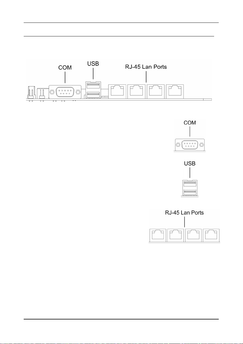
BACK PANEL PORTS
The back panel has the following po rts:
Serial port: COM 1
The 9-pin COM 1 port is for pointing devices or other
serial devices.
USB 2.0 ports
The USB ports is for connecting to extern al periphera l
devices.
Installation
RJ-45 10/100 LAN ports
The mainboard provides four standard RJ-45
ports which allow connection to a Local Area
Network (LAN).
11
Page 20
Chapter 2
CONNECTORS
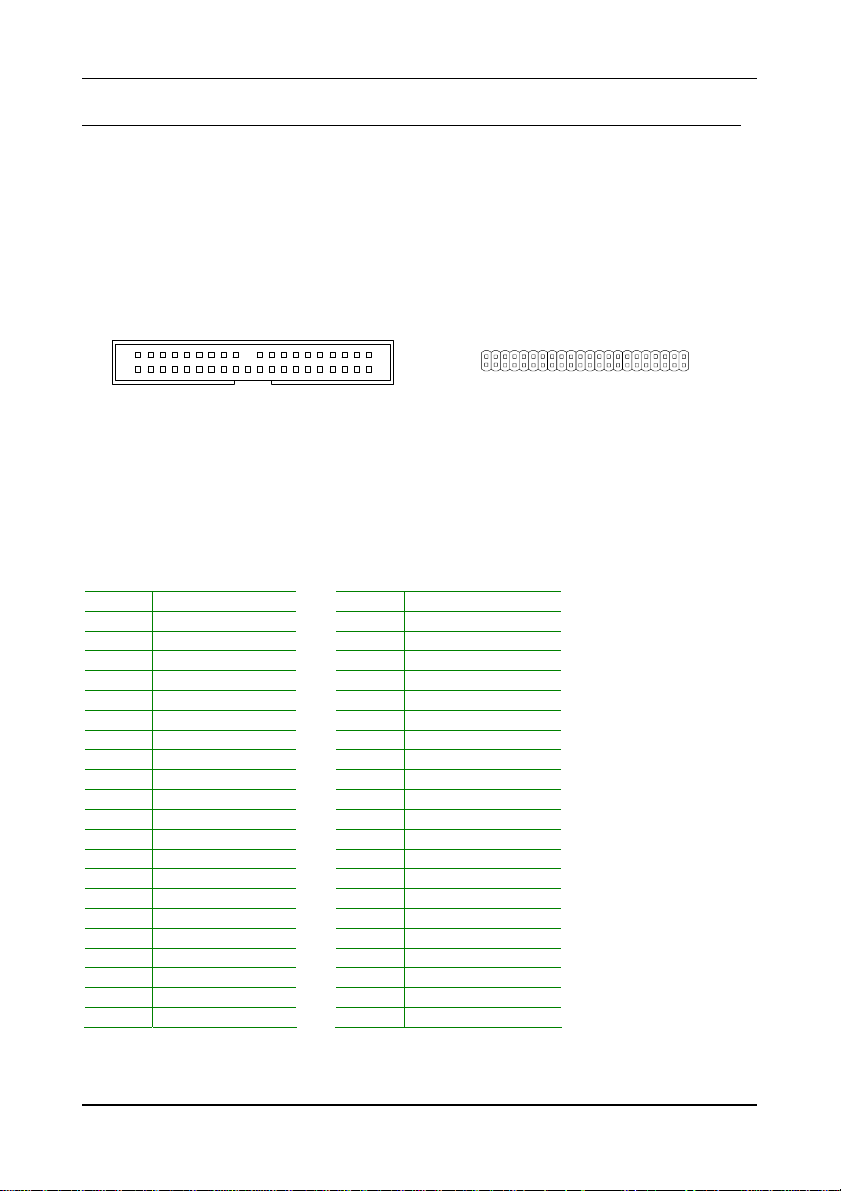
Hard Disk Connectors: IDE1 & IDE2
The mainboard has an Ultra DMA 133/100/66 controller. You can connect up
to four hard disk drives, CD-ROM and other dev ices.
The primary hard drive should always be connected to IDE1 as the master
drive. Both IDE drives can connect to a master an d a slave drive .
IDE1 (40 pins)
1
IDE2 (44 pins)
1
If two drives are connected to a single ca ble, the jumper on the secon d drive
must be set to slave mode. Refer to the d rive documentation supplied by the
vendor for the jumper settings.
IDE2 Pinout:
Pin Signal Pin Signal
1 -IDERST2 2 GND
3 SDD7 4 SDD8
5 SDD6 6 SDD9
7 SDD5 8 SDD10
9 SDD4 10 SDD11
11 SDD3 12 SDD12
13 SDD2 14 SDD13
15 SDD1 16 SDD14
17 SDD0 18 SDD15
19 GND 20 NC
21 SDDREQ 22 GND
23 -SDIOW 24 GND
25 -SDIOR 26 GND
27 SHDRDY 28 NC
29 -SDDACK 30 GND
31 IRQ15 32 NC
33 SDA1 34 S_ATA66
35 SDA0 36 SDA2
37 -SCS1 38 -SCS3
39 -HD_led2 40 GND
41 +5V 42 +5V
43 GND 44 NC
12
Page 21

Installation
Case Connector: F_PANEL
The F_PANEL pin header allows you to connect the power switch, reset switch,
power LED, sleep LED, HDD LED and the case s peaker.
Pin Signal Pin Signal
1 +5V 2 +5V
3 +5V 4 HD_LED
5 -PLED_2 6 PW_BN
7 +5V 8 GND
9 NC 10 RST_SW
11 NC 12 GND
13 SPEAK 14 +5V
15 Key 16 -SLEEP_LED
F_PANEL
12
15 16
HDD LED (HD_LED): pin 2 & pin 4
HDD LED shows the activity of a hard disk drive. Avoid turn ing the power off
when the HDD LED still has a lit. Connect the HDD LED from the system case
to this pin.
Power Switch (PW_BN): pin 6 & pin 8
Connect to a 2-pin power button switch. Pressing this button will turn the
system power on or off.
Reset Switch (RST_SW): pin 10 & pin 12
The reset switch is used to rebo ot the system rather than turning the power
ON/OFF. Avoid rebooting the system, if the HDD is still working. Connect
the reset switch from the system case to this pin.
Sleep LED (-SLEEP_LED): pin 14 and pin 16
Power LED (-PLED_2): pin 1 & pin 5, or pin 3 & pin 5
The LED will light when the system is on. If the system is in S1 (POS - Power
On Suspend) or S3 (STR - Suspend To RAM) state, the LED will b link.
Speaker (SPEAK): pin 7 & pin 13
The speaker from the system case is connected to this pin.
13
Page 22
Chapter 2
Serial ATA Connectors: SATA1 and SATA2
These next generation connectors support the thin Serial ATA
cables for primary internal storage devices. The current Serial
ATA interface allows up to 150 MB/s data transfer rate, faster
than the standard parallel ATA with 133 MB/s (Ultra DMA).
VGA Connectors
The internal pin header is to suppor t VGA outpu t.
Pin Signal Pin Signal
1 GND 2 VCC
3 R 4 SPD2
5 G 6 SPCLK2
7 B 8 HSYNC
9 GND 10 VSYNC
11 GND 12 GND
13 GND 14 Key
SATA1-2
VGA1
12
13
14
14
Page 23
Installation
USB Pin Connector: USB 2-4
The mainboard provides 3 front USB pin headers, allowing up to 6 additional
USB 2.0 ports up to maximum throughput of 480 Mbps. Connect each 2-port
USB cable into the pin header. This port can be used to connect high-speed
USB interface peripherals such as USB HDD, digital cameras, MP3 players,
printers, modem and the like.
USB2
11
1
2
12
Pin Signal Pin Signal
1 VCC 2 VCC
3 USBD_T2- 4 USBD_T35 USBD_T2+ 6 USBD_T3+
7 GND 8 GND
9 Key 10 Wireless LAN LED
11 NC 12 NC
USB3
Pin Signal Pin Signal
1 VCC 2 VCC
3 USBD_T4- 4 USBD_T55 USBD_T4+ 6 USBD_T5+
7 GND 8 GND
9 Key 10 GND
12
910
USB4
Pin Signal Pin Signal
1 5VDUAL 2 5VDUAL
3 USBD_T6- 4 USBD_T75 USBD_T6+ 6 USBD_T7+
7 GND 8 GND
9 Key 10 GND
12
910
15
Page 24

Chapter 2
Serial Port Connector: COM 2/3/4
COM2/3/4 pin headers can be used to attach additional ports for serial mouse
or other serial devices.
COM2
Pin Signal Pin Signal
1 RIN12 2 RIN32
3 DOUT22 4 DOUT32
5 GND 6 RIN22
7 DOUT12 8 RIN42
9 XRI2# 10 Key
12
910
COM3
Pin Signal Pin Signal
1 RIN13 2 RIN33
3 DOUT23 4 DOUT33
5 GND 6 RIN23
7 DOUT13 8 RIN43
9 XRI3# 10 Key
12
910
Pin Signal Pin Signal
1 RIN14 2 RIN34
3 DOUT24 4 DOUT34
5 GND 6 RIN24
7 DOUT14 8 RIN44
9 XRI4# 10 Key
COM4
12
910
16
Page 25

Installation
Digital I/O Connector: DIO
General purpose input and output.
DIO
Pin Signal Pin Signal
1 +5V 2 +12V
3 GPO14 4 GPI20
5 GPO13 6 GPI21
7 GPO4 8 GPI22
9 GPO29 10 GPI9
11 GND 12 GND
12
11
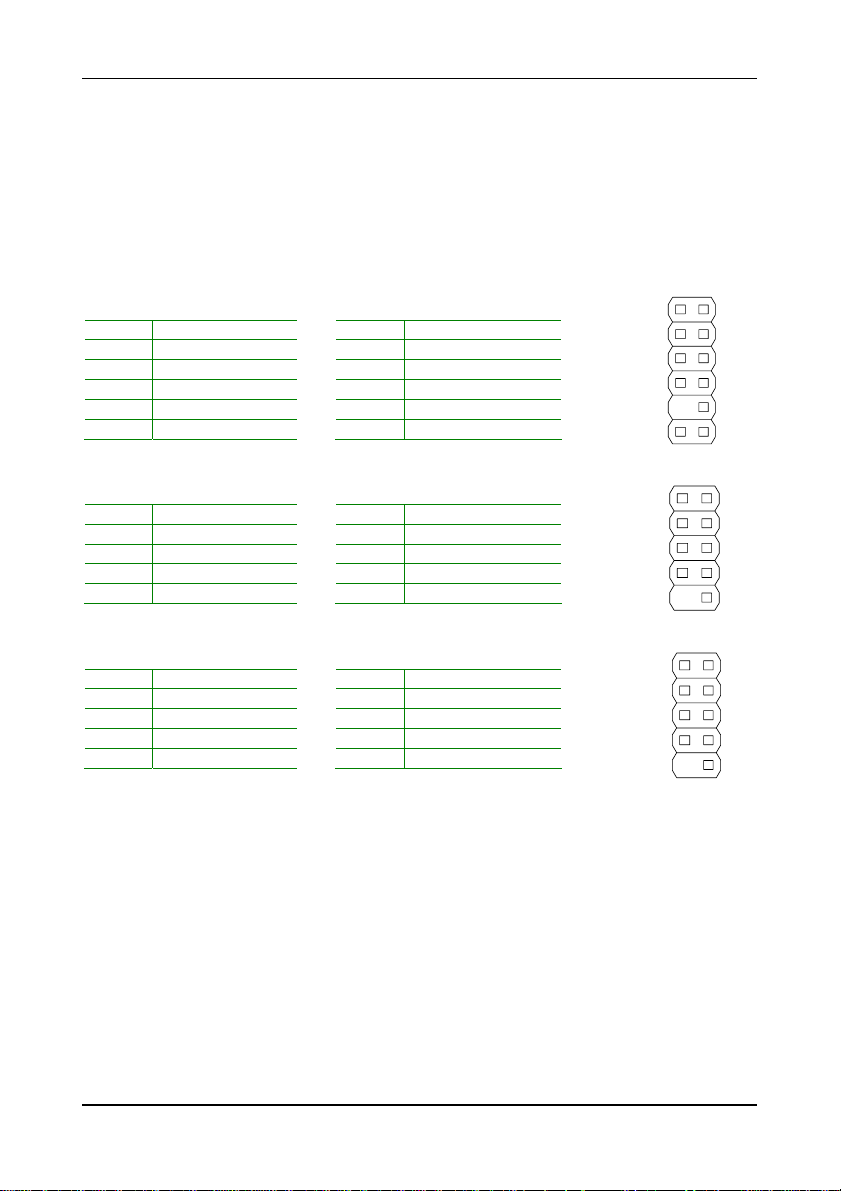
KBMS Connector: JKB/MS
The mainboard provides a PS2 pin header to attach a PS 2 keyboard and
mouse.
JKB/MS
Pin Signal Pin Signal
1 VCCE 2 VCCE
3 KB_CLK 4 Key
5 EKBCLK 6 EKBDATA
7 KB_DT 8 MS_DT
9 KB_CK 10 MS_CK
12
Note: When the pin header is not in use, please short pi n 3&5, pin
4&6, pin 7&9 and pin 8&10.
12
109
LAN LED Connector: J3
This pin header allows you to connect to a LAN LED which shows the state of
network connecion.
J3
Pin Signal Pin Signal
1 LAN1_ACT 2 LINK_UP1
3 LAN2_ACT 4 LINK_UP2
5 LAN3_ACT 6 LINK_UP3
7 LAN4_ACT 8 LINK_UP4
9 Key 10 NC
11 +3.3V 12 WireLess LED
17
12
11
12
Page 26

Chapter 2
JUMPERS
The mainboard provides jumpers for setting some mainboard functions. Th is
section will explain how to change the settings of the mainboard functions
using the jumpers.
Clear CMOS Connector: CLEAR_CMOS
The onboard CMOS RAM stores system configuration d ata and has an
onboard battery power supply. To reset the CMOS settings, set the jumper
on pins 1 and 2 while the system is off. R eturn the jumper to p ins 2 and 3
afterwards. Setting the jumper while the system is on will damage the
mainboard.
Setting 1 2 3
Normal Operation ON ON OFF
Clear CMOS setting OFF ON ON
WARNING: Except when clearing the RTC RAM, never remove the
cap on CLEAR_CMOS jumper default position. Removing the cap will
cause system boot failure. Avoid clearing the CMOS while the system
is on; it will damage the mainboard.
Normal:
132
Clear:
132
LAN3-LAN4 Bypass Enable: J2
Open 1-2, bypass function is enabled for LAN3 and LAN4; sh ort
1-2, then bypass function is disabled.
J2
1
18
Page 27

Installation
BIOS Write Protection: WP1
This jumper allows you to protect from flas hing the BIOS. BIOS Write
Protection setting: pin1 = /WP & /TBL, pin2 = GND, short 1-2.
Watchdog Timer: WDTO1
Watchdog Timer setting: pin1 = -WDTO, p in2 = VCORE GD, short 1 -2.
S_LED1
Pin header for LED indicator of SATA HD, short 1-2.
WP1
1
WDTO1
1
S_LED1
1
19
Page 28

Chapter 2
SLOTS
Peripheral Component Interconnect: Mini PCI
The Mini PCI interface is designed for the BXB Expansion module for
supporting additional functi ons as 1 Mini-PCI slot, 1 CF card reader interface,
and 2 x 44 pin IDE conne ctors. Among th ose 2 IDE connecto rs, one of them
has the DOM support.
Mini PCI 1-2
1
PCI Interrupt Request Routing
The IRQ (interrupt request line) are hardware lines over which devices can
send interrupt signals to the microprocessor . The PCI pins ar e typically
connected to the PCI bus as follows:
INTA# INTB#
Slot 1 INT C# INT D#
20
Page 29

HAPTER
C
3
BIOS Setup
This chapter gives a detailed explanation of the BIOS setup functions.
21
Page 30

Chapter 3
ENTERING SETUP
Power on the computer and press <Delete> during the beginning of the boot
sequence to enter the BIOS setup menu. If you missed the BIOS setu p entry
point, you may restart the system and try again.
22
Page 31

BIOS Setup
CONTROL KEYS
Keys Description
Up Arrow Move to the previous item
Down Arrow Move to the next item
Left Arrow Move to the item in the left side
Right Arrow Move to the item in the right side
Enter Select the item
Escape Jumps to the Exit menu or returns to the main menu from a
Page Up / + Increase the numeric valu e or make changes
Page Down / - Decrease the numeric valu e or make chang es
F1 General help, only for Sta tus Page Setup Menu and Option
F5 Restore the previous CMOS value from CMOS, only for
F6 Load the default CMOS value from Fail-Safe default table,
F7 L oad Optimized defa ults
F9 J umps to the Mai n Menu
F10 Save all the CMOS changes and exit
submenu
Page Setup Menu
Option Page Setup Menu
only for Option Page Setup Menu
23
Page 32

Chapter 3
NAVIGATING THE BIOS MENUS
The main menu displays all the BIOS setu p categories. Use the control keys
Up/Down arrow keys to select any item/sub-menu. Description of the
selected/highlighted category is disp layed at the bottom of the scre en.
An arrow symbol next to a field indicates that a sub-menu is availa ble (see
figure below). Press <Enter> to display the sub-menu. To exit the submenu, press <Esc>.
24
Page 33

BIOS Setup
GETTING HELP
The BIOS setup program provides a “General He lp” screen. You can display
this screen from any menu/sub-menu by pressing <F1>. The help screen
displays the keys for using and navigating the BIOS setup. Press <Esc> to
exit the help screen.
25
Page 34

Chapter 3
MAIN MENU
Phoenix - AwardBIOS CMOS Setup Utility
Standard CMOS Features
Advanced BIOS Features
Advanced Chipset Features
Integrated Peripherals
Power Management Setup
PnP / PCI Configurations
Frequency / Voltage Control
Esc : Quit
F10 : Save & Exit Setup
Time, Date, Hard Disk Type...
Load Fail-Safe Defaults
Load Optimized Defaults
Set Supervisor Password
Set User Password
Save & Exit Setup
Exit Without Saving
: Select ItemF9 : Menu in BIOS
Standard CMOS Features
Use this menu to set basic system configurations.
Advanced BIOS Features
Use this menu to set the advanced features available on your system.
Advanced Chipset Features
Use this menu to set chipset specific features and optimize system
performance.
Integrated Peripherals
Use this menu to set onboard peripherals f eatures.
Power Management Setup
Use this menu to set onboard power managemen t functions .
PnP/PCI Configurations
Use this menu to set the PnP and PCI configurat ions.
26
Page 35

BIOS Setup
Frequency/Voltage Control
Use this menu to set the system frequency and voltage control.
Load Fail-Safe Defaults
Use this menu option to load the BIOS default settings for minimal and stable
system operations.
Load Optimized Defaults
Use this menu option to load BIOS default settings for optimal and high
performance system operations.
Set Supervisor Password
Use this menu option to set the BI OS supe rvisor pass word.
Set User Password
Use this menu option to set the BI OS user password .
Save & Exit Setup
Save BIOS setting changes and exit setu p.
Exit Without Saving
Discard all BIOS setting changes and exit setup.
27
Page 36

Chapter 3
STANDARD CMOS FEATURES
Phoenix - AwardBIOS CMOS Setup Utility
Standard CMOS Features
Apr
Date (mm:dd:yy)
Time (hh:mm:ss)
IDE Channel 0 Master
IDE Channel 0 Slave
IDE Channel 1 Master
IDE Channel 1 Slave
Halt On [All , But Keyboard]
Base Memory 640K
Extended Memory 15360K
Total Memory 16384K
Tue,
20
20 20
:
21 2004
:
Item Help
Menu Level
Change the day, month,
year and century
: Move
Enter: Select +/-/PU/PD: Value F10: Save ESC: Exit F1: General Help
F5: Previous Values F6: Fail-Safe Defaults F7: Optimized Defaults
Date
The date format is [Day, Month Date Year]
Time
The time format is [Hour : Minute : Secon d]
Halt On
Sets the system’s response to specific boot errors. Below is a table that
details the possible settings .
Setting Description
All Errors System halts when any error is detected
No Errors System does not halt for any error
All, But Keyboard System halts for all non-key errors
28
Page 37

IDE DRIVES
IDE HDD Auto-Detection
IDE Channel 0 Master [Auto]
Access Mode [Auto]
Capacity 0 MB
Cylinder 0
Head 0
Precomp 0
Landing Zone 0
Sector 0
PIO Mode [Auto]
Ultra DMA Mode [Auto]
Phoenix - AwardBIOS CMOS Setup Utility
IDE Channel 0 Master
[Press Enter]
BIOS Setup
Item Help
Menu Level
To auto-detect the HDD's
size, head... on this channel
: Move
Enter: Select +/-/PU/PD: Value F10: Save ESC: Exit F1: General Help
F5: Previous Values F6: Fail-Safe Defaults F7: Optimized Defaults
The specifications of your drive must match with the drive table. The hard
disk will not work properly if you enter incorrect information in this category.
Select “Auto” whenever possible. If you select “Manual”, make sure the
information is from your hard disk ven dor or system manufacturer. Below is
a table that details required hard drive information when using the “Manual”
mode.
Setting Description
IDE Channel The name of this match the name of the menu.
Access Mode Settings: [CHS, LBA, Large, Auto]
Capacity Formatted size of the storage device
Cylinder Number of cylinders
Head Number of heads
Precomp Write precompensation
Landing Zone Cylinder location of the landing zone
Sector Number of sectors
PIO Mode Settings: [Auto, 0, 1, 2, 3, 4]
Ultra DMA Mode Settings: [Disabled, Auto]
Settings: [None, Auto, Manual]
29
Page 38

Chapter 3
ADVANCED BIOS FEATURES
Phoenix - AwardBIOS CMOS Setup Utility
Advanced BIOS Features
CPU Feature [Press Enter]
Hard Disk Boot Priority [Press Enter]
Virus Warning [Disabled]
CPU L1 & L2 Cache [Enabled]
Quick Power On Self Test [Enabled]
First Boot Device [USB-FDD]
Second Boot Device [CDROM]
Third Boot Device [Hard Disk]
Boot Other Device [Enabled]
Boot Up NumLock Status [On]
Typematic Rate Setting [Enabled]
Typematic Rate (Chars/Sec) 6
Typematic Delay (Msec)
Security Option [Setup]
APIC Mode [Enabled]
MPS Version Control For OS [1.4]
Console Redirection
Baud Rate [19200]
Agent Connect via
Agent wait time(min)
Agent after boot
Display Full Screen Logo
Display Small Logo
250
Enabled
NULL
1
Disabled
[Enabled]
[Disabled]
Item Help
Menu Level
: Move
Enter: Select +/-/PU/PD: Value F10: Save
F5: Previous Values F6: Fail-Safe Defaults F7: Optimized Defaults
ESC: Exit F1: General Help
Virus Warning
Setting Description
Enabled Turns on hard disk boot sector virus protection
Disabled Turns off hard disk boot sector virus protection
CPU L1 & L2 Cache
Setting Description
Enabled Turns on CPU L1 & L2 cache
Disabled Turns off C PU L 1 & L2 c ache
30
Page 39

BIOS Setup
Quick Power On Self-Test
Shortens Power On Self-Test (POST) cy cle to enable sh orter boot up time.
Setting Description
Enabled Shorten Power On Self Test (POS T) cycle and bootup ti me
Disabled Standard Power On Self Test (POST)
First/Second/Third Boot Device
Set the boot device sequence as BIOS attempts to load the disk operating
system.
Setting Description
LS120 Boot from LS-120 drive
Hard Disk Boot from the HDD
CDROM Boot from CD-ROM
ZIP100 Boot from ATAPI ZIP drive
USB-FDD Boot from USB floppy drive
USB-ZIP Boot from USB ZIP drive
USB-CDROM Boot from USB CDROM
Legacy LAN Boot from network driv e
Disabled Disable the boot device sequence
Boot Other Device
Enables the system to boot from alternate devices if the system fails to boot
from the “First/Second/Third Boot Device” list.
Setting Description
Enabled Enable alternate boot device
Disabled No alternate boot device allowed
Boot Up NumLock Status
Set the NumLock status when the system is power ed on.
Setting Description
On Forces keypad to behave as 10-key
Off Forces keypad to behave as arrow keys
Typematic Rate Setting
Enables “Typematic Rate” and “Typemat ic Delay” functi ons.
Settings: [Enabled, Disabled]
31
Page 40

Chapter 3
Security Option
Selects whether the password is required every time the System boots, or
only when you enter Setup.
Setting Description
Setup Password prompt appears only when end users try to run BIOS
System Password prompt appears every time when the computer is
Setup
powered on and when end users try to run BIOS Setup
APIC Mode
Enables APIC (Advanced Programmable Interrupt Controller) functionality.
Settings: [Enabled, Disabled]
MPS Variation Control For OS
Settings: [1.1, 1.4]
Baud Rate
Settings: [9600, 19200, 38400, 57600, 11 5200]
Display Full Screen Logo
Show full screen logo during BIOS boot up process.
Settings: [Enabled, Disabled]
Display Small Logo
Show small energy star logo during BIOS boot up process.
Settings: [Enabled, Disabled]
32
Page 41

CPU FEATURE
Delay Prior to Thermal
Thermal Management
TM2 Bus Ratio
TM2 Bus VID
Execute Disable Bit
C7 CMPXCHG8
C7 NoExecute (NX)
C7 TM1/TM2 Woking Temp 'C
C7 TM Overstress Temp 'C
ODCM
Phoenix - AwardBIOS CMOS Setup Utility
CPU Feature
[16 Min]
[Thermal Monitor 1]
[ 0 X]
[0.716V]
[Enabled]
[Enabled]
[Disabled]
[100]
[125]
[Disabled]
BIOS Setup
Item Help
Menu Level
: Move
Enter: Select +/-/PU/PD: Value F10: Save ESC: Exit F1: General Help
F5: Previous Values F6: Fail-Safe Defaults F7: Optimized Defaults
Delay Prior to Thermal
Settings: [4 Min, 8 Min, 16 Min, 32 Min]
Thermal Management
Thermal Monitor 1 (On die throtting) ; Thermal Monitor 2 (Ratio & VID
transition).
Settings: [Thermal Monitor 1, Therma l Monito r 2]
TM2 Bus Ratio
Represent the frequency (bus ratio) of the throttled performance state that
will be initiated when the on-die sensor goes from not hot to hot.
Settings: [Key in a DEC number ranged be tween 0~255 ]
33
Page 42

Chapter 3
TM2 Bus VID
Represent the voltage of the throttle d performance state that wi ll be initiated
when the on-die sensor goes from not ho t to hot.
Settings: [0.700, 0.716, 0.732, 0.748, 0.764, 0.780, 0.796, 0.812, 0.828,
0.844, 0.860, 0.876, 0.892, 0.908, 0.924, 0.940, 0.956, 0.972, 0.988, 1.004,
1.020, 1.036, 1.052, 1.068, 1.084, 1.100, 1.116, 1.132, 1.148, 1.164, 1.180,
1.196, 1.212, 1.228, 1.244, 1.260, 1.276, 1.292, 1.308, 1.324, 1.340, 1.356,
1.372, 1.388, 1.404, 1.420, 1.436, 1.452, 1.468, 1.484, 1.500, 1.516, 1.532,
1.548, 1.564, 1.580, 1.596, 1.612, 1.628, 1.644, 1.660, 1.676, 1.692, 1.708]
Execute Disable Bit
When disabled, forces the XD feature flag to always return to 0.
Settings: [Enabled, Disabled]
C7 CMPXCHG8
Disable to install Windows NT 4.0.
Settings: [Enabled, Disabled]
C7 NoExecute (NX)
NoExecute is supported in WinXP SP2 and provides some protection from virii.
Settings: [Enabled, Disabled]
C7 TM1/TM2 Working Temp ℃
Show small energy star logo during BIOS boot up process.
Settings: [Enabled, Disabled]
C7 TM Overstress Temp ℃
Settings: [Key in a DEC number ranged be tween 0~255 ]
ODCM
On Demand Clock Modulation forces an internal stop grant duty cycle.
Settings: [Disabled, 12.5%, 25.0%, 37.5%, 50.0%, 62 .5%, 75.0%, 87.5%]
34
Page 43

HARD DISK BOOT PRIORITY
Phoenix - AwardBIOS CMOS Setup Utility
Hard Disk Boot Priority
1.
Pri. Master :
Pri. Master :
2.
Pri. Master :
3.
Pri. Master :
4.
Pri. Slave :
5.
Sec. Master :
6.
Sec. Slave :
7.
USBHDD1 :
8.
Item Help
Menu Level
Use < > or < > to
select a device, then
press < + > to move it
up, or < - > to move it
down the list. Press
<ESC> to exit this
menu.
BIOS Setup
: Move
F5: Previous Values F6: Fail-Safe Defaults F7: Optimized Defaults
PU/PD/+/-:Change Priority F10: Save
ESC: Exit
This is for setting the priority of the har d disk b oot order wh en the “Hard
Disk” option is selected in th e “[Firs t/Seco nd/Third] Boot Device” menu item .
35
Page 44

Chapter 3
ADVANCED CHIPSET FEATURES
Phoenix - AwardBIOS CMOS Setup Utility
Advanced Chipset Features
Display Card Priority
AGP & P2P Bridge Control
CPU & PCI Bus Control
AGP Driving Control
AGP Driving Value
Select Display Device
Panel Type
[PCI Slot]
[Press Enter]
[Press Enter]
[AUTO]
DA
CRT
[01]
Item Help
Menu Level
If there are display cards on
both AGP and PCI slots,
configure this item for BIOS
to select which one to boot
: Move
Enter: Select +/-/PU/PD: Value F10: Save ESC: Exit F1: General Help
F5: Previous Values F6: Fail-Safe Defaults F7: Optimized Defaults
WARNING: The Advanced Chipset Features menu is used for
optimizing the chipset func tions. Do not chan ge these settings unless
you are familiar with the chipset.
Display Card Priority
This setting specifies which VGA card is your primary graphics adapter.
Settings: [PCI Slot, AGP]
AGP Driving Control
Always fix this setting to opti mized defau lt value unless you face problems
with special video cards.
Settings: [Auto, Manual]
36
Page 45

BIOS Setup
Panel Type
This setting refers to the native resolution of the display being used wit h the
system.
Settings: [Key in a HEX number ranged between 0000 ~000F]
37
Page 46

Chapter 3
AGP & P2P BRIDGE CONTROL
Phoenix - AwardBIOS CMOS Setup Utility
AGP & P2P Bridge Control
AGP Aperture Size [128M]
AGP 2.0 Mode [1X]
AGP Fast Write [Disabled]
AGP 3.0 Calibration cycle [Enabled]
VGA Share Memory Size [64M]
Direct Frame Buffer
[Enabled]
Item Help
Menu Level
: Move
Enter: Select +/-/PU/PD: Value F10: Save ESC: Exit F1: General Help
F5: Previous Values F6: Fail-Safe Defaults F7: Optimized Defaults
AGP Aperture Size
This setting controls how much memory space can be allocated to AGP for
video purposes. The aperture is a portion of the PCI memory address range
dedicated to graphics memory address space. Host cycles that hit the
aperture range are forwarded to the AGP without any transla tion.
Settings: [32MB, 64MB, 128MB, 256MB, 512MB, 1G]
AGP 2.0 Mode
To configure the maximum capable performance of the AGP bus. The actual
performance depends on the display card.
Settings: [4X, 2X, 1X]
AGP Fast Write
Enable this feature can improve system performance. Enable ONLY when
your AGP Card supports Fast Write.
Settings: [Enabled, Disabled]
38
Page 47

AGP 3.0 Calibration cycle
Settings: [Enabled, Disabled]
VGA Share Memory Size
Settings: [Disabled, 16M, 32M, 64M]
Direct Frame Buffer
Settings: [Enabled, Disabled]
BIOS Setup
39
Page 48

Chapter 3
CPU & PCI BUS CONT ROL
Phoenix - AwardBIOS CMOS Setup Utility
CPU & PCI Bus Control
[By Auto]VLink mode selection
[Enabled]VLink 8X Support
[Default]DRDY_Timing
Item Help
Menu Level
: Move
Enter: Select +/-/PU/PD: Value F10: Save ESC: Exit F1: General Help
F5: Previous Values F6: Fail-Safe Defaults F7: Optimized Defaults
V-Link mode selection
This menu item controls the data transfer speed between the north and south
bridge.
Settings: [By Auto, Mode 0~4]
V-Link 8X Support
Settings: [Enabled, Disabled]
DRDY_Timing
Settings: [Slowest, Default, Optimize]
40
Page 49

INTEGRATED PERIPHERALS
Phoenix - AwardBIOS CMOS Setup Utility
Integrated Peripherals
Onboard IDE Channel 1 [Enabled]
Onboard IDE Channel 2 [Enabled]
IDE Prefetch Mode [Enabled]
IDE HDD Block Mode [Enabled]
OnChip SATA [Enabled]
SATA Mode [RAID]
OnChip USB Controller [All Enabled]
OnChip EHCI Controller [Enabled]
USB Emulation [ON]
Onboard Serial Prot 1 [3F8]
Serial Prot 1 Use IRQ [IRQ4]
Onboard Serial Prot 2 [2F8]
Serial Prot 2 Use IRQ [IRQ3]
Onboard Serial Prot 3 [3E8]
Serial Prot 3 Use IRQ [IRQ5]
Onboard Serial Prot 4
Serial Prot 4 Use IRQ
Watch Dog Timer Select
[2E8]
[IRQ10]
[Disabled]
BIOS Setup
Item Help
Menu Level
To control the onboard
primary IDE Channel. Choose
"Disabled" if you do not have
any device connected
: Move
Enter: Select +/-/PU/PD: Value F10: Save ESC: Exit F1: General Help
F5: Previous Values F6: Fail-Safe Defaults F7: Optimized Defaults
Onboard IDE Channel 1 and 2
The integrated peripheral controller contains an IDE interface with sup port for
two IDE channels.
Setting Description
Enabled Activates each channel separately
Disabled Deactivates IDE chan nels
IDE Prefetch Mode
Fixed to default “Enabled” to let the IDE controller work more efficiently.
Settings: [Enabled, Disabled]
IDE HDD Block Mode
If your IDE hard drive supports block mode, select Ena bled for auto matic
detection of the optimal number of block read/write per sector the drive can
support.
Settings: [Enabled, Disabled]
41
Page 50

Chapter 3
OnChip SATA
Settings: [Enabled, Disabled]
SATA Mode
Serial ATA is the latest generation of the A TA interfa ce. Serial ATA h ard
drives deliver transfer speeds of up to 150MB/se c.
Setting Description
IDE Supports two SATA plus two PATA hard disk drives
RAID Only SATA supports RAID
OnChip USB Controller
Settings: [All Disabled, All Enabled, 1&2 USB Port, 2&3 USB Port, 1&3 USB
Port, 1 USB Port, 2 US B Port , 3 USB Port]
OnChip EHCI Controller
Settings: [Enabled, Disabled]
USB Emulation
Set this field to choose the US B emula tion. When set to “OF F “, do n ot
support any USB device on DOS. When set to “KB/MS”, support USB legacy
keyboard and mouse, no support USB storage. And set to ”ON”, support USB
legacy keyboard, mouse and storage.
Settings: [OFF, KB/MS, ON]
Onboard Serial Port 1
Settings: [Disabled, 3F8, 2F8, 3E8, 2E8]
Serial Prot 1 USB IRQ
Settings: [IRQ3, IRQ 4, IRQ 5, IRQ 10, IRQ 11]
Onboard Serial Port 2
Settings: [Disabled, 3F8, 2F8, 3E8, 2E8]
Serial Prot 2 USB IRQ
Settings: [IRQ3, IRQ 4, IRQ 5, IRQ 10, IRQ 11]
42
Page 51

Onboard Serial Port 3
Settings: [Disabled, 3F8, 2F8, 3E8, 2E8]
Serial Prot 3 USB IRQ
Settings: [IRQ3, IRQ 4, IRQ 5, IRQ 10, IRQ 11]
Onboard Serial Port 4
Settings: [Disabled, 3F8, 2F8, 3E8, 2E8]
Serial Prot 4 USB IRQ
Settings: [IRQ3, IRQ 4, IRQ 5, IRQ 10, IRQ 11]
Watchdog Timer Select
Settings: [Disabled, 20 Sec, 30 Sec, 40 Sec, 1 M in, 2 Min, 4 Min ]
BIOS Setup
43
Page 52

Chapter 3
POWER MANAGEMENT SETUP
Phoenix - AwardBIOS CMOS Setup Utility
Power Management Setup
HDD Power Down
Power Management Timer [Disabled]
Video Off Option [Suspend -> Off]
AC Loss Auto Restart [On]
Peripherals Activities [Press Enter]
IRQs Activities [Press Enter]
[ 1 Min]
Item Help
Menu Level
Select the idle time before
hard disk go into power
saving mode.
: Move
Enter: Select +/-/PU/PD: Value F10: Save ESC: Exit F1: General Help
F5: Previous Values F6: Fail-Safe Defaults F7: Optimized Defaults
HDD Power Down
Sets the length of time for a period of inactivity before powering down the
hard disk.
Settings: [Disabled, 1~15 (minutes) ]
Power Management Timer
Set the idle time before system enters power saving mode. ACPI OS such as
Windows XP will overrid e thi s opti on.
Settings: [Disabled, 1/2/4/6/8/10/20/30/40 (minutes), 1 (hour)]
Video Off Option
Select whether or not to turn off the screen when system enters power
saving mode, ACPI OS such as Windows XP will ov erride th is opt ion.
Setting Description
Always On Screen is always on even when system enters power saving
Suspend -> Off Screen is turned off when system enters power saving mode
mode
44
Page 53

BIOS Setup
AC Loss Auto Restart
The field defines how the system will respond after an AC power loss during
system operation.
Setting Description
Off Keeps the system in an off state until the power button is
On Restarts the system when the power is back
Former-Sts Former-Sts
pressed
45
Page 54

Chapter 3
PERIPHERAL ACTIVITIES
Phoenix - AwardBIOS CMOS Setup Utility
Peripherals Activities
VGA Event [OFF]
COM Event
HDD Event
PCI Master Event
PowerOn by PCI Card
Wake Up On LAN/Ring [Disabled]
RTC Alarm Resume [Disabled]
Date (of Month)
Resume Time (hh:mm:ss)
[COM]
[ON]
[OFF]
[Disabled]
0
0: 0: 0
Item Help
Menu Level
Decide whether or not
the power management
unit should monitor
VGA activities.
: Move
Enter: Select +/-/PU/PD: Value F10: Save ESC: Exit F1: General Help
F5: Previous Values F6: Fail-Safe Defaults F7: Optimized Defaults
VGA Event
Enables the power management unit to monitor VGA activities.
Settings: [Off, On]
COM Event
Decide whether or not the power management unit should monitor serial port
(COM) activities.
Settings: [None, COM]
HDD Event
Enables the power management unit to monitor hard disk activities.
Settings: [Off, On]
PCI Master Event
Enables the power management unit to monitor PCI master activities.
Settings: [Off, On]
46
Page 55

BIOS Setup
PowerOn by PCI Card
Enables activity detected from any PCI card to power up the system or
resume from a suspended state. Such P CI cards in clude LAN card, onb oard
LAN controller, onboard USB ports, etc.
Settings: [Disabled, Enabled]
Wake Up On LAN/Ring
Decide whether or not any Ring-In signals from Modem can wake up the
system from a suspended state.
Settings: [Disabled, Enabled]
RTC Alarm Resume
Sets a scheduled time and/or date to automatically power on the system.
Settings: [Disabled, Enabled]
Date (of Month)
The field specifies the date for “RTC Alarm Resume”.
Resume Time (hh:mm:ss)
The field specifies the time for “RTC Alarm Resume”.
47
Page 56

Chapter 3
IRQS ACTIVITIES
Phoenix - AwardBIOS CMOS Setup Utility
Primary INTR [ON]
IRQ3 (COM 2) [Enabled]
IRQ4 (COM 1) [Enabled]
IRQ5 (COM 3) [Enabled]
IRQ6 (Floppy Disk) [Disabled]
IRQ7 (Reserved) [Disabled]
IRQ8 (RTC Alarm) [Disabled]
IRQ9 (IRQ2 Redir) [Disabled]
IRQ10 (COM 4) [Enabled]
IRQ11 (Reserved) [Disabled]
IRQ12 (PS/2 Mouse) [Enabled]
IRQ13 (Coprocessor) [Enabled]
IRQ14 (Hard Disk) [Enabled]
IRQ15 (Reserved) [Disabled]
IRQs Activities
Item Help
Menu Level
If you choose Disabled, the
power management unit will
not monitor any IRQ activities.
: Move
Enter: Select +/-/PU/PD: Value F10: Save ESC: Exit F1: General Help
F5: Previous Values F6: Fail-Safe Defaults F7: Optimized Defaults
Primary INTR
Restores the system to an active state if IRQ activity is detected from any of
the enabled channels
Settings: [Off, On]
IRQ3~IRQ15
Enables or disables the monitoring of the specified IRQ line. These fields are
only available if “Primary INTR” is on.
Settings: [Enabled, Disabled]
Note: IRQ (Interrupt Request) lines are system res ources alloc ated to
I/O devices. When an I/O device needs to gain attention of the
operating system, it signals this by causing an IRQ to occur. After
receiving the signal, when the operating system is ready, the system
will interrupt itself and perform the service required by the IO device.
48
Page 57

PNP/PCI CONFIGURATIONS
Phoenix - AwardBIOS CMOS Setup Utility
PnP / PCI Configurations
PNP OS Installed [No]
Reset Configuration Data [Disabled]
Resources Controlled By [Auto(ESCD)]
IRQ Resources Press Enter
Assign IRQ For VGA [Enabled]
Assign IRQ For USB [Enabled]
BIOS Setup
Item Help
Menu Level
Select Yes if you are using a
Plug and Play capable
operating system. Select No
if you need the BIOS to
configure non-boot devices.
: Move
Enter: Select +/-/PU/PD: Value F10: Save ESC: Exit F1: General Help
F5: Previous Values F6: Fail-Safe Defaults F7: Optimized Defaults
Note: This section covers some very technical items and it is strongly
recommended to leave the default settings as is unless you are an
experienced user.
PNP OS Installed
Setting Description
Yes BIOS will only initialize the PnP cards used for booting (VGA,
No BIOS will initialize all the PnP cards
IDE, SCSI). The rest of the cards will be initialized by the
PnP operating system
49
Page 58

Chapter 3
Reset Configuration Data
This field should usually be left “Disabled”.
Setting Description
Enabled Resets the ESCD (Extended System Configuration Data)
Disabled Default setting
after exiting BIOS Setup if a newly installed PCI card or the
system configuration prevents the operating system from
loading
Resource Controlled By
Enables the BIOS to automatically conf igure all the Plug-and-Play compatible
devices.
Setting Description
Auto(ESCD) BIOS will automatically assign IRQ, DMA and memory base
Manual Unlocks “IRQ Resources” for manual configuration
address fields
Assign IRQ For VGA/USB
Assign IRQ for VGA and USB devices.
Settings: [Disabled, Enabled]
50
Page 59

FREQUENCY / VOLT AGE CONTROL
Phoenix - AwardBIOS CMOS Setup Utility
Frequency / Voltage Control
DRAM Clock [By SPD]
DRAM Timing [Auto By SPD]
SDRAM CAS Latency 2.5
Bank Interleave Disabled
Precharge to Active(Trp) 2T
Active to Precharge(Tras) 07T
Active to CMD(Trcd) 4T
REF to ACT/REF (Trfc) 15T
ACT(0) to ACT(1) (TRRD) 3T
Read to Precharge (Trtp) [3T]
Write to Read CMD (Twtr) [1T/2T]
Write Recovery Time (Twr) [4T]
RDSAIT mode
RDSAIT selection
Auto Detect PCI Clk
CPU Clock
CPU Clock Ratio
Spread Spectrum
[2T Command]DRAM Command Rate
[Auto]
03
[Enabled]
[100MHz]
[ 6 X]
[0.25%]
BIOS Setup
Item Help
Menu Level
: Move
Enter: Select +/-/PU/PD: Value F10: Save ESC: Exit F1: General Help
F5: Previous Values F6: Fail-Safe Defaults F7: Optimized Defaults
DRAM Clock
The chipset supports synchronous and asynchronous mode between host
clock and DRAM clock frequency.
Settings: [By SPD, 100 MHz, 133 MHz, 166 MHz , 200MHz, 2 66MHz]
DRAM Timing
The value in this field depends on the memory modules installed in your
system. Changing the value from the factory setting is not recommended
unless you install new memory that has a different performance rating than
the original modules.
Settings: [Manual, Auto By SPD, Turbo, Ultra]
Read to Precharge (Trtp)
Settings: [2T, 3T]
Write to Read CMD (Twtr)
Settings: [1T/2T, 2T/3T]
51
Page 60

Chapter 3
Write Recovery Time (Twr)
Settings: [2T, 3T, 4T, 5T]
DRAM Command Rate
This field is for setting how fast the memory controller sends out commands.
Lower setting equals faster command rate.
Note: Some memory modules may not be able to handl e lower
settings.
Settings: [2T Command, 1T Command]
RDSAIT mode
Settings: [Manual, Auto]
Auto Detect PCI Clk
Settings: [Enabled, Disabled]
CPU Clock
Settings: [Key in a DEC number ranged be tween 100~33 3]
CPU Clock Ratio
To configure the CPU internal clock multiplier. This option does NOT apply to
CPU(s) which have this clock multiplier locked.
Settings: [Key in a DEC number ranged be tween 8~50]
Spread Spectrum
When the mainboard's clock generator pulses, the extreme values (spikes ) of
the pulses creates EMI (Electromagnetic I nterference). The Spread Spectru m
function reduces the EMI generated by modulating the pulses so that the
spikes of the pulses are redu ced to fla tter curves .
Settings: [Disabled, 0.20%, 0.25%, 0.35%]
52
Page 61

LOAD FAIL-SAFE DEFA ULT S
Phoenix - AwardBIOS CMOS Setup Utility
BIOS Setup
Standard CMOS Features
Advanced BIOS Features
Advanced Chipset Features
Integrated Peripherals
Power Management Setup
PnP / PCI Configurations
Frequency / Voltage Control
Esc : Quit
F10 : Save & Exit Setup
Load Fail-Safe Defaults (Y/N)?
Load Fail-Safe Defaults
Load Fail-Safe Defaults
Load Optimized Defaults
Set Supervisor Password
Set User Password
Save & Exit Setup
N
Exit Without Saving
: Select ItemF9 : Menu in BIOS
This option is for restoring all the default fail-safe BIOS settings. These
values are set by the mainboard manufacturer to provide a stable system with
basic performance.
Entering “Y” loads the default fail-safe BIOS values.
53
Page 62

Chapter 3
LOAD OPTIMIZED DEFAULTS
Phoenix - AwardBIOS CMOS Setup Utility
Standard CMOS Features
Advanced BIOS Features
Advanced Chipset Features
Integrated Peripherals
Power Management Setup
PnP / PCI Configurations
Frequency / Voltage Control
Esc : Quit
F10 : Save & Exit Setup
Load Optimized Defaults (Y/N)?
Load Optimized Defaults
Load Fail-Safe Defaults
Load Optimized Defaults
Set Supervisor Password
Set User Password
Save & Exit Setup
Exit Without Saving
N
: Select ItemF9 : Menu in BIOS
This option is for restoring all the default optimized BIOS settings. The
default optimized values are set by th e mainboard manufacturer to provide a
stable system with optimized performance.
Entering “Y” loads the default optimized BIOS values.
54
Page 63

SET SUPERVISOR / USER PASSWORD
Phoenix - AwardBIOS CMOS Setup Utility
BIOS Setup
Standard CMOS Features
Advanced BIOS Features
Advanced Chipset Features
Integrated Peripherals
Power Management Setup
PnP / PCI Configurations
Frequency / Voltage Control
Esc : Quit
F10 : Save & Exit Setup
Enter Password:
Change / Set / Disable Password
Load Fail-Safe Defaults
Load Optimized Defaults
Set Supervisor Password
Set User Password
Save & Exit Setup
Exit Without Saving
Save & Exit Setup
: Select ItemF9 : Menu in BIOS
This option is for setting a password for entering BIOS Setup. When a
password has been set, a password prompt will b e displayed whenever BIOS
Setup is run. This prevents an unauthorized person from changing any part
of your system configuration.
There are two types of passwords you can set. A supervis or password and a
user password. When a supervisor password is used, the BIOS Setup
program can be accessed and the BIOS settings can be changed. When a
user password is used, the BIOS Setup program can be accessed but the
BIOS settings cannot be changed.
To set the password, type the password (up to eight characters in length)
and press <Enter>. The password typed now will clear any previously set
password from CMOS memory. The new password will need to be reentered
to be confirmed. To cancel the process pre ss <Esc>.
55
Page 64

Chapter 3
To disable the password, press <Enter> when prompted to enter a new
password. A message will show up to confirm disabling the password. To
cancel the process press <Esc>.
Additionally, when a password is enabled, the BIOS can be se t to request the
password each time the system is booted . This would prevent unauthorized
use of the system. See “Security Option ” in the “Advanced BIOS Features”
section for more details .
56
Page 65

SAVE & EXIT SETU P
BIOS Setup
Phoenix - AwardBIOS CMOS Setup Utility
Standard CMOS Features
Advanced BIOS Features
Advanced Chipset Features
Integrated Peripherals
Power Management Setup
PnP / PCI Configurations
Frequency / Voltage Control
Esc : Quit
F10 : Save & Exit Setup
SAVE to CMOS & EXIT (Y/N)?
Save Data to CMOS
Load Fail-Safe Defaults
Load Optimized Defaults
Set Supervisor Password
Set User Password
Save & Exit Setup
N
Exit Without Saving
: Select ItemF9 : Menu in BIOS
Entering “Y” saves any changes made and exits the program.
Entering “N” will cancel the exit request.
57
Page 66

Chapter 3
EXIT WITHOUT SAVING
Phoenix - AwardBIOS CMOS Setup Utility
Standard CMOS Features
Advanced BIOS Features
Advanced Chipset Features
Integrated Peripherals
Power Management Setup
PnP / PCI Configurations
Frequency / Voltage Control
Esc : Quit
F10 : Save & Exit Setup
Quit Without Saving (Y/N)?
Abandon all Data
Load Fail-Safe Defaults
Load Optimized Defaults
Set Supervisor Password
Set User Password
Save & Exit Setup
Exit Without Saving
N
: Select ItemF9 : Menu in BIOS
Entering “Y” discards any changes made and exits the program.
Entering “N” will cancel the exit request.
58
Page 67

HAPTER
C
4
Driver Installation
This chapter gives you brief descriptions of ea ch mainboard dr iver and
application. You must install the VIA chipset drivers first before
installing other drivers such as audio or VGA drive rs. The applications
will only function correctly if the necessary drivers are already
installed.
59
Page 68

Chapter 4
DRIVER UTILITIES
Getting Started
The Driver Utilities CD contains the driver utilities and software for enhancing
the performance of the mainboard.
Note: The driver utilities and software are updated from time to time. The
latest updated versions are avai lable at http:// www. viaem bedde d.com. /
60
Page 69

Driver Installation
Running the Driver Utilities CD
To start using the CD, insert the CD into the CD-ROM or DVD-ROM drive.
The CD should run automatically afte r clos ing the C D-ROM or DVD-RO M drive .
The driver utilities and software menu screen should then appear on the
screen. If the CD does not run automatically, click on the “Start” button and
select “Run…” Then type: "D:\Setup.exe".
Note: D: might not be the drive letter of the CD-ROM/DVD-ROM in
your system.
61
Page 70

Chapter 4
CD CONTENT
VIA 4in1 Drivers: Contains VIA ATAPI Vendor Support
Driver (enables the performance enhancing bus mastering
functions on ATA-capable Hard Disk Drives and ensures IDE
device compatibility), AGP VxD Driver (provides servi ce routines
to your VGA driver and interface di rectly to hardware, providin g
fast graphical access), IRQ Routing Miniport Driver (sets the
system's PCI IRQ routing sequence) and VIA INF Driver
(enables the VIA Power Management function).
VIA Graphics Driver: Enhances the onboard VIA graphic
chip.
VIA Audio Driver: Enhances the onboard VIA audio chip.
VIA USB 2.0 Driver: Enhances VIA USB 2.0 ports.
Intel LAN Driver: Enhances the onboard Inte l 10/100M LAN
chip.
Intel GigaLAN Driver: Enhances the onboard optional Intel
10/100/1000M LAN chip.
VIA RAID Driver: Support for RAID devices.
62
Page 71

PPENDIX
A
Watchdog Timer Configuration
The WDT is used to generate a varie ty of output signals after a user
programmable count. The WDT is suitable for use in the prevention
of system lock-up, such as when software becomes trapped in a
deadlock. Under these sort of circumstances, the timer w ill count to
zero and the selected outputs will be driven. Under normal
circumstance, the user will restart the WDT at reg ular intervals before
the timer counts to zero.
63
Page 72

Appendix
SAMPLE CODE
This code and information is provided “as is” without warranty of any kind,
either expressed or implied, including but not limited to the implied
warranties of merchantability and/or fitness for a particular pu rpose.
#include <stdio.h>
#include <dos.h>
#include <inlines/pc.h>
//Sio area
#define SUPERIO_INDEX 0x4e
#define SUPERIO_DATA 0x4f
#define BANK_REG 0x07
#define CR20_R EG 0x20 //This register indicate the device's ID
#define Fintek_ID 0x08 //Fintek Device ID CR21-20 = 0208h
//Digital Input=GP10~13 ==> mapping to IN0~I N3
//Digital Output=GP14~17 ==> ma pping t o OUT0~OUT 3
main(int argc, char *argv[])
{
int i;
int io_mode; //0: read 1:write
char *ptr;
unsigned char tmp, tmp1;
64
Page 73

Watchdog Timer Configuration
int value;
printf("===========================================
=============================\n");
printf(" Fintek Watchdog testing program Ver :00 2007 -2-5\n");
printf("===========================================
=============================\n");
if (detect_sio()) print_err_help(argv);
if ((argc<2)||(argc>3))
{
print_help(argv);
}
// printf("the parameter=%s \n", argv[1 ]);
sscanf(argv[1], "%d", &value);
// printf("you input=%d\n", value);
if(value >255) print_help(argv);
write_sio_reg(0x08, 0x60, 0x03); //Set Watch Dog timer base
address High byte = 03h
write_sio_reg(0x08, 0x61, 0x00); //Set Watch Dog timer base
address Low byte = 00h
write_sio_reg(0x08, 0x30, 0x01); //enable watchdog function
65
Page 74

Appendix
outportb(0x0300, 0x03); //Select unit to one se cond and clear time
out status
outportb(0x0301, value);
outportb(0x0301, value); //S et timer t o value second a nd enable
timer
printf("Program %d seconds success\n", value);
return;
}
void print_help(char *argv[])
{
printf("!!! Wrong argument !!!\n");
printf("using: %s nnn\n", argv[0]);
printf(" nnn=1~255 seconds\n");
printf(" nnn=0 to disbale watchdog \n");
printf("Program terminated !!!\n");
exit(1);
}
void print_err_help(char *argv[])
{
printf("!!! Wrong platform !!!\n");
printf("!!! This is not Fintek \n");
printf("!!! Program terminated !!!\n");
exit(1);
}
66
Page 75

Watchdog Timer Configuration
//input: none
//output: 1 = not correct SuperI O
// 0 = correct SuperIO
int detect_sio(void)
{
//check the SuperIO version
if(read_sio_reg(0,CR20_REG)==Fintek_ID)
return 0;
else
return 1;
}
unsigned char read_sio_reg(int bank_no, int reg_n o)
{
unsigned char reg_data;
enter_sio_config();
outportb(SUPERIO_INDEX, BANK_REG);
delay(1);
outportb(SUPERIO_DATA, bank_no);
delay(1);
outportb(SUPERIO_INDEX, reg_no);
delay(1);
reg_data=inportb(SUPERIO_DATA);
exit_sio_config();
return reg_data;
67
Page 76

Appendix
}
void write_sio_reg(int bank_no, int reg_no , unsigned short wr ite_data)
{
enter_sio_config();
outportb(SUPERIO_INDEX, BANK_REG);
delay(1);
outportb(SUPERIO_DATA, bank_no);
delay(1);
outportb(SUPERIO_INDEX, reg_no);
delay(1);
outportb(SUPERIO_DATA, write_data);
exit_sio_config();
}
void enter_sio_config()
{
outportb(SUPERIO_INDEX, 0x77);
delay(1); //delay some time
outportb(SUPERIO_INDEX, 0x77);
}
void exit_sio_config()
{
outportb(SUPERIO_INDEX, 0xaa);
}
68
 Loading...