

Page 1

1.04-04082019-104700
USER MANUAL
VIA ETX-8X90
Computer-On-Module
Page 2

Copyright
Copyright © 2014-2019 VIA Technologies Incorporated. All rights reserved.
No part of this document may be reproduced, transmitted, transcribed, stored in a retrieval system, or translated into any language,
in any form or by any means, electronic, mechanical, magnetic, optical, chemical, manual or otherwise without the prior written
permission of VIA Technologies, Incorporated.
Trademarks
All trademarks are the property of their respective holders.
Disclaimer
No license is granted, implied or otherwise, under any patent or patent rights of VIA Technologies. VIA Technologies makes no
warranties, implied or otherwise, in regard to this document and to the products described in this document. The information
provided in this document is believed to be accurate and reliable as of the publication date of this document. However, VIA
Technologies assumes no responsibility for the use or misuse of the information (including use or connection of extra
device/equipment/add-on card) in this document and for any patent infringements that may arise from the use of this document. The
information and product specifications within this document are subject to change at any time, without notice and without obligation
to notify any person of such change.
VIA Technologies, Inc. reserves the right the make changes to the products described in this manual at any time without prior notice.
Regulatory Compliance
FCC-A Radio Frequency Interference Statement
This equipment has been tested and found to comply with the limits for a class A digital device, pursuant to part 15 of the FCC rules.
These limits are designed to provide reasonable protection against harmful interference when the equipment is operated in a
commercial environment. This equipment generates, uses, and can radiate radio frequency energy and, if not installed and used in
accordance with the instruction manual, may cause harmful interference to radio communications. Operation of this equipment in a
residential area is likely to cause harmful interference, in which case the user will be required to correct the interference at his
personal expense.
Notice 1
The changes or modifications not expressly approved by the party responsible for compliance could void the user's authority to
operate the equipment.
Notice 2
Shielded interface cables and A.C. power cord, if any, must be used in order to comply with the emission limits.
Notice 3
The product described in this document is designed for general use, VIA Technologies assumes no responsibility for the conflicts or
damages arising from incompatibility of the product. Check compatibility issue with your local sales representatives before placing
an order.
Page 3

Battery Recycling and Disposal
Only use the appropriate battery specified for this product.
Do not re-use, recharge, or reheat an old battery.
Do not attempt to force open the battery.
Do not discard used batteries with regular trash.
Discard used batteries according to local regulations.
Safety Precautions
Always read the safety instructions carefully.
Keep this User's Manual for future reference.
All cautions and warnings on the equipment should be noted.
Keep this equipment away from humidity.
Put this equipment on a reliable flat surface before setting it up.
Check the voltage of the power source and adjust to 110/220V before connecting the equipment to
the power inlet.
Do not place the power cord where people will step on it.
Always unplug the power cord before inserting any add-on card or module.
If any of the following situations arise, get the equipment checked by authorized service personnel:
The power cord or plug is damaged.
Liquid has entered into the equipment.
The equipment has been exposed to moisture.
The equipment is faulty or you cannot get it work according to User's Manual.
The equipment has been dropped and damaged.
The equipment has an obvious sign of breakage.
Do not leave this equipment in extreme temperatures or in a storage temperature above 60°C (140°F).
The equipment may be damaged.
Do not leave this equipment in direct sunlight.
Never pour any liquid into the opening. Liquid can cause damage or electrical shock.
Do not place anything over the power cord.
Do not cover the ventilation holes. The openings on the enclosure protect the equipment from
overheating.
Page 4

VIA ETX-8X90 User Manual
iv
Box Contents
Items for STK-E8X90-00A0
1 x ETX-8X90 ETX module board
1 x ETXDB1 ETX carrier board
1 x SATA cable
1 x PATA cable
1 x KB/MS cable
1 x COM cable
1 x LPT cable
Items for STK-E8X90-01A0
1 x ETX-8X90 module
1 x ETXDB1 carrier board
1 x SATA cable
1 x PATA cable
1 x KB/MS cable
1 x COM cable
1 x LPT cable
1 x LVDS cable
1 x Inverter cable
1 x 12.1”LCM
Ordering Information
Part Number Description
10GAB12A00020
ETX Board with 1.2GHz VIA Nano® X2 E-Series CPU with VGA, LVDS,
4 USB 2.0, 2 Mini USB 2.0, COM, 10/100Mbps Ethernet, SATA, 2 IDE,
2 PCI, Micro SD card slot, ATX power connector
ETXDB1
ETX-8X90 evaluation carrier board
99G42-01381Q
Heatsink with fan for ETX-8X90 (with ETXDB1)
99G42-01390Q
Heat Spreader for ETX-8X90 (with ETXDB1)
99G42-01469Q
Heat Spreader for ETX-8X90
STK-E8X90-00A0
ETX-8X90 Starter Kit
STK-E8X90-01A0
ETX-8X90 Starter Kit with Panel
Page 5

VIA ETX-8X90 User Manual
v
Table of Contents
1. Product Overview ........................................................................................................................ 1
1.1. Key Components ............................................................................................................................................... 1
1.1.1. VIA Nano® X2 E-Series Processor .......................................................................................................... 1
1.1.2. VIA VX900 MSP Chipset ........................................................................................................................... 1
1.2. Product Specifications ...................................................................................................................................... 2
1.3. Layout Diagram .................................................................................................................................................. 4
1.4. Product Dimensions .......................................................................................................................................... 5
2. I/O Interface................................................................................................................................... 6
2.1. Micro SD Card Slot ........................................................................................................................................... 6
2.2. Mini USB 2.0 Ports ............................................................................................................................................. 6
2.3. SATA Connectors .............................................................................................................................................. 7
2.4. VGA Connector ................................................................................................................................................. 8
2.5. DC-in Connector ................................................................................................................................................ 9
2.6. CPU and System Fan Connectors ................................................................................................................... 9
2.7. HDD Selector Switch .....................................................................................................................................10
2.8. Clear CMOS Jumper .......................................................................................................................................11
2.9. LPC Connector .................................................................................................................................................12
2.10. SPI Connector ...................................................................................................................................................13
2.11. ETX Connectors ...............................................................................................................................................14
2.11.1. ETX Connector X1 (CNX1) ....................................................................................................................15
2.11.2. ETX Connector X2 (CNX2) ....................................................................................................................16
2.11.3. ETX Connector X3 (CNX3) ....................................................................................................................17
2.11.4. ETX Connector X4 (CNX4) ....................................................................................................................18
3. Hardware Installation ................................................................................................................ 19
3.1. Mounting VIA ETX-8X90 module onto the ETXDB1 carrier board .....................................................19
4. BIOS Setup Utility ...................................................................................................................... 23
4.1. Entering the BIOS Setup Utility ....................................................................................................................23
4.2. Control Keys .....................................................................................................................................................23
4.3. Navigating the BIOS Menus ...........................................................................................................................23
4.4. Getting Help .....................................................................................................................................................23
4.5. System Overview .............................................................................................................................................24
4.5.1. AMIBIOS .....................................................................................................................................................24
4.5.2. Processor ....................................................................................................................................................24
4.5.3. System Memory ........................................................................................................................................24
4.5.4. System Time ..............................................................................................................................................24
4.5.5. System Date ...............................................................................................................................................24
4.6. Advanced Settings...........................................................................................................................................25
4.6.1. CPU Configuration ....................................................................................................................................26
4.6.2. SATA Configuration .................................................................................................................................26
4.6.2.1. Hard Disk Information ..................................................................................................................27
4.6.2.1.1. PIO Mode ................................................................................................................................27
4.6.2.1.2. DMA Mode .............................................................................................................................27
4.6.3. SuperIO Configuration ............................................................................................................................28
4.6.3.1. Serial Ports 1 to 2 Address and IRQ ........................................................................................28
4.6.3.2. Serial Port 2 Mode .......................................................................................................................28
4.6.3.3. Parallel Port Address ...................................................................................................................28
4.6.3.4. Parallel Port Mode .......................................................................................................................28
4.6.3.5. Parallel Port IRQ ...........................................................................................................................28
4.6.4. Hardware Health Configuration ............................................................................................................29
4.6.4.1. Smart FAN 1 and FAN 2..............................................................................................................29
4.6.5. ACPI Configuration...................................................................................................................................30
4.6.5.1. Suspend Mode ..............................................................................................................................30
4.6.5.2. ACPI Version Features .................................................................................................................30
4.6.6. APM Configuration ...................................................................................................................................31
Page 6

VIA ETX-8X90 User Manual
vi
4.6.6.1. Power Button Mode .....................................................................................................................31
4.6.6.2. Restore on AC/Power Loss .........................................................................................................31
4.6.6.3. Resume On PCI PME#..................................................................................................................31
4.6.6.4. Resume On KBC ............................................................................................................................32
4.6.6.5. Wake-Up Key .................................................................................................................................32
4.6.6.6. Wake-Up Password ......................................................................................................................32
4.6.6.7. Resume On PS/2 Mouse ..............................................................................................................32
4.6.6.8. Resume on RTC Alarm ................................................................................................................32
4.6.6.9. RTC Alarm Date (Days) ...............................................................................................................32
4.6.6.10. System Time ...................................................................................................................................33
4.6.7. Spread Spectrum Configuration ............................................................................................................33
4.6.7.1. CPU Spread Spectrum Setting ...................................................................................................33
4.6.8. USB Configuration ....................................................................................................................................34
4.6.9. CRB Configuration ....................................................................................................................................34
4.6.9.1. DRAM Clock ..................................................................................................................................35
4.6.9.2. Select Display Device 1 and 2 ..................................................................................................35
4.6.9.3. Panel Type ......................................................................................................................................35
4.6.9.4. VGA Share Memory (Frame Buffer) ..........................................................................................35
4.6.9.5. OnChip HDAC Device ................................................................................................................35
4.6.9.6. SMBus Device Switch...................................................................................................................35
4.6.9.7. SDIO Host controller ..................................................................................................................35
4.6.9.8. WATCH-DOG ...............................................................................................................................35
4.6.9.9. Unit-Select .....................................................................................................................................35
4.6.9.10. Time-Select ....................................................................................................................................36
4.6.9.11. Backlight Control ..........................................................................................................................36
4.6.9.12. Backlight PWM Clock ..................................................................................................................36
4.6.9.13. LAN Boot ROM .............................................................................................................................36
4.7. Boot Settings .....................................................................................................................................................37
4.7.1. Boot Settings Configuration ...................................................................................................................37
4.7.1.1. Quick Boot .....................................................................................................................................38
4.7.1.2. Quiet Boot ......................................................................................................................................38
4.7.1.3. Bootup Num-Lock ........................................................................................................................38
4.7.1.4. Wait for ‘F1’ if Error ......................................................................................................................38
4.7.1.5. Hit ‘DEL’ Message Display ..........................................................................................................38
4.7.2. Boot Device Priority .................................................................................................................................39
4.7.2.1. 1st Boot Device ..............................................................................................................................39
4.8. Security Settings ...............................................................................................................................................40
4.8.1. Change Supervisor Password ................................................................................................................40
4.8.2. User Access Level ....................................................................................................................................40
4.8.3. Change User Password............................................................................................................................41
4.8.4. Clear User Password ...............................................................................................................................41
4.8.5. Password Check ........................................................................................................................................41
4.9. Exit Options ......................................................................................................................................................42
4.9.1. Save Changes and Exit ............................................................................................................................42
4.9.2. Discard Changes and Exit .......................................................................................................................42
4.9.3. Discard Changes .......................................................................................................................................42
4.9.4. Load Optimal Defaults ...........................................................................................................................42
5. Software and Technical Support ............................................................................................. 43
5.1. Microsoft and Linux Support.........................................................................................................................43
5.1.1. Driver Installation .....................................................................................................................................43
5.2. Technical Support and Assistance ...............................................................................................................43
Appendix A. ETXDB1 Carrier Board Reference ................................................................................ 44
A.1. Board Specifications ...........................................................................................................................................44
A.1.1. Board Storage Channel Configuration ....................................................................................................45
A.2. External I/O Connectors ....................................................................................................................................46
A.2.1. Rear I/O Ports ...............................................................................................................................................46
A.3. ETXDB1 Layout Diagram ...................................................................................................................................47
Page 7

VIA ETX-8X90 User Manual
vii
A.3.1. Onboard Connectors and Slots ...............................................................................................................47
A.3.2. Onboard Pin headers and Jumpers .........................................................................................................48
A.3.3. Connectors and Slots Pin Definition .......................................................................................................49
A.3.3.1. ATX1 : 20-pin ATX Power Connector .........................................................................................49
A.3.3.2. ISA1: ISA Slot .....................................................................................................................................50
A.3.3.3. PCI1 and PCI2: PCI Slots ..................................................................................................................51
A.3.3.4. IDE1 and IDE2: IDE Connector ......................................................................................................53
A.3.3.5. LVDS1: LVDS Panel Connector ......................................................................................................54
A.3.3.6. BL1: Backlight Connector ................................................................................................................54
A.3.3.7. CNX1~ CNX4: ETX Connector X1, X2, X3 and X4 ..................................................................55
A.3.4. Pin Headers Definition and Jumper Settings .........................................................................................59
A.3.4.1. F_AUDIO1 and I2C1: Front Audio and I²C Pin Headers ..........................................................59
A.3.4.2. SIR1 and SMB1: Serial Infrared and SMBus Pin Headers ..........................................................60
A.3.4.3. F_PANEL1 and LPT1: Front Panel and LPT Pin Headers ...........................................................61
A.3.4.4. COM2 and KBMS1: COM and Keyboard & Mouse Pin Headers ...................................................62
A.3.4.5. J1: Backlight and Panel Power Jumper .........................................................................................63
A.4. ETXDB1 Dimensions ...........................................................................................................................................64
A.4.1. ETXDB1 Board Dimensions .......................................................................................................................64
A.4.2. ETXDB1 External I/O Dimensions ...........................................................................................................64
Page 8

VIA ETX-8X90 User Manual
viii
List of Figures
Figure 1: Layout diagram of the VIA ETX-8X90 module (top side) .........................................................................4
Figure 2: Layout diagram of the VIA ETX-8X90 module (bottom side) ..................................................................4
Figure 3: Dimensions of the VIA ETX-8X90 module (top view) ...............................................................................5
Figure 4: Dimensions of the VIA ETX-8X90 module (bottom view) ........................................................................5
Figure 5: Micro SD card slot diagram ..............................................................................................................................6
Figure 6: Mini USB 2.0 ports diagram ..............................................................................................................................6
Figure 7: SATA connectors diagram ................................................................................................................................7
Figure 8: VGA connector diagram ....................................................................................................................................8
Figure 9: DC-in connector diagram ..................................................................................................................................9
Figure 10: CPU and System fan connectors diagram ...................................................................................................9
Figure 11: HDD selector DIP switch diagram ............................................................................................................. 10
Figure 12: Clear CMOS jumper diagram ...................................................................................................................... 11
Figure 13: LPC connector diagram ................................................................................................................................ 12
Figure 14: SPI connector diagram .................................................................................................................................. 13
Figure 15: ETX connectors diagram .............................................................................................................................. 14
Figure 16: Carrier board ETX connectors and mounting holes .............................................................................. 19
Figure 17: Installing the VIA ETX-8X90 module on the carrier board ................................................................. 19
Figure 18: Installing the DDR3 SODIMM memory module ..................................................................................... 20
Figure 19: Removing the thermal pad cover ............................................................................................................... 20
Figure 20: Heatsink/heat spreader’s mounting holes on VIA ETX-8X90 module............................................... 21
Figure 21: Installing the heatsink/heat spreader on VIA ETX-8X90 module ....................................................... 21
Figure 22: Securing the heatsink/heat spreader and VIA ETX-8X90 module ...................................................... 22
Figure 23: Illustration of the Main menu screen ......................................................................................................... 24
Figure 24: Illustration of the Advanced Settings screen .......................................................................................... 25
Figure 25: Illustration of the CPU Configuration screen ........................................................................................... 26
Figure 26: Illustration of SATA Configuration screen ............................................................................................... 26
Figure 27: Illustration of SATA-1 Primary IDE screen ............................................................................................... 27
Figure 28: Illustration of SuperIO Configuration screen .......................................................................................... 28
Figure 29: Illustration of Hardware Health Configuration screen .......................................................................... 29
Figure 30: Illustration of ACPI Configuration screen ................................................................................................. 30
Figure 31: Illustration of APM Configuration screen ................................................................................................. 31
Figure 32: Illustration of Spread Spectrum Configuration screen .......................................................................... 33
Figure 33: Illustration of USB Configuration screen .................................................................................................. 34
Figure 34: Illustration of CRB Configuration screen .................................................................................................. 34
Figure 35: Illustration of Boot Settings screen ............................................................................................................ 37
Figure 36: Illustration of Boot Settings Configuration screen ................................................................................. 37
Figure 37: Illustration of Boot Device Priority screen ............................................................................................... 39
Figure 38: Illustration of Security Settings screen ...................................................................................................... 40
Figure 39: Illustration of Exit Options screen ............................................................................................................. 42
Figure 40: Rear I/O ports ................................................................................................................................................. 46
Figure 41: ETXDB1 connectors and slots diagram .................................................................................................... 47
Figure 42: ETXDB1 pin headers and jumpers diagram ............................................................................................. 48
Figure 43: ATX Power connector diagram .................................................................................................................. 49
Figure 44: ISA slot diagram ............................................................................................................................................. 50
Figure 45: PCI slot diagram ............................................................................................................................................. 51
Figure 46: IDE connector diagram ................................................................................................................................. 53
Figure 47: LVDS panel connector diagram.................................................................................................................. 54
Figure 48: Backlight connector diagram ....................................................................................................................... 54
Figure 49: ETX connector X1, X2, X3 and X4 diagram ............................................................................................ 55
Figure 50: Front audio and I²C pin headers diagram ................................................................................................. 59
Figure 51: Serial Infrared and SMBus pin headers diagram ..................................................................................... 60
Figure 52: Front panel and LPT pin headers diagram ............................................................................................... 61
Figure 53: COM and keyboard & mouse pin headers diagram............................................................................... 62
Figure 54: Backlight and Panel power jumper diagram ............................................................................................ 63
Figure 55: ETXDB1 board dimensions diagram .......................................................................................................... 64
Figure 56: ETXDB1 External I/O dimensions diagram ............................................................................................... 64
Page 9

VIA ETX-8X90 User Manual
ix
List of Tables
Table 1: Micro SD card slot pinouts ................................................................................................................................6
Table 2: Mini USB 2.0 ports pinouts ................................................................................................................................6
Table 3: SATA connectors pinouts ..................................................................................................................................7
Table 4: VGA connector pinouts .....................................................................................................................................8
Table 5: DC-in connector pinouts ....................................................................................................................................9
Table 6: CPU and System fan connectors pinouts .......................................................................................................9
Table 7: IDE1 and SATA2 HDD configuration (default setting) ............................................................................ 10
Table 8: IDE1 and IDE2 HDD configuration (manufacturing option 1) ................................................................ 10
Table 9: Clear CMOS jumper settings ......................................................................................................................... 11
Table 10: LPC connector pinouts .................................................................................................................................. 12
Table 11: SPI connector pinouts.................................................................................................................................... 13
Table 12: ETX connector X1 pinouts ........................................................................................................................... 15
Table 13: ETX connector X2 pinouts ........................................................................................................................... 16
Table 14: ETX connector X3 pinouts ........................................................................................................................... 17
Table 15: ETX connector X4 pinouts ........................................................................................................................... 18
Table 16: Serial port addresses and IRQs ................................................................................................................... 28
Table 17: Panel types resolution ................................................................................................................................... 35
Table 18: ETXDB1 and VIA ETX-8X90 storage configuration ................................................................................ 45
Table 19: Description table of the ETXDB1 connectors and slots ....................................................................... 47
Table 20: Description table of the ETXDB1 pin headers and jumpers ................................................................ 48
Table 21: ATX Power connector pinouts .................................................................................................................... 49
Table 22: ISA slot pinouts............................................................................................................................................... 50
Table 23: PCI slot 1 pinouts ........................................................................................................................................... 51
Table 24: PCI slot 2 pinouts ........................................................................................................................................... 52
Table 25: IDE connector pinouts ................................................................................................................................... 53
Table 26: LVDS panel connector pinouts ................................................................................................................... 54
Table 27: Backlight connector pinouts ........................................................................................................................ 54
Table 28: ETX connector X1 pinouts ........................................................................................................................... 55
Table 29: ETX connector X2 pinouts ........................................................................................................................... 56
Table 30: ETX connector X3 pinouts ........................................................................................................................... 57
Table 31: ETX connector X4 pinouts ........................................................................................................................... 58
Table 32: Front audio pin header pinouts ................................................................................................................... 59
Table 33: I²C pin header pinouts ................................................................................................................................... 59
Table 34: Serial Infrared pin header pinouts .............................................................................................................. 60
Table 35: SMBus pin header pinouts ............................................................................................................................ 60
Table 36: Front panel pin header pinouts ................................................................................................................... 61
Table 37: LPT pin header pinouts ................................................................................................................................. 61
Table 38: COM pin header pinouts .............................................................................................................................. 62
Table 39: Keyboard & mouse pin header pinouts ..................................................................................................... 62
Table 40: Backlight and Panel power jumper settings ............................................................................................. 63
Page 10

VIA ETX-8X90 User Manual
1
1. Product Overview
The VIA ETX-8X90 is a compact and highly integrated Computer-On-Module based on standard
Embedded Technology eXtended form factor. It comes with power efficient 1.2GHz VIA Nano® X2
E-Series processor, and VIA VX900 MSP chipset featuring the VIA C-9 HD DX9 with 3D/2D graphics and
video decoding accelerator for rich digital media performance, and provides support for extensive
connectivity options including USB, Ethernet, Audio, PCI, ISA, IDE and graphics through board-to-board
connectors to an I/O carrier board. The VIA ETX-8X90 module is designed for embedded applications
such as industrial PC, medical PC, test machines, measuring equipment, monitoring system, etc.
1.1. Key Components
1.1.1. VIA Nano® X2 E-Series Processor
The VIA Nano® X2 E-Series is a 64-bit superscalar x86 dual core processor based on a 40 nanometer
process technology. Packed into an ultra-compact NanoBGA2 package (measuring 21mm x 21mm), it
delivers an energy-efficient yet powerful performance, with cool and quiet operation. The VIA Nano X2
E-Series processor is ideal for embedded system applications such as industrial PCs, test machines,
measuring equipment, digital signage, medical PCs, monitoring systems, gaming machines, in-vehicle
entertainment, etc.
Note:
For Windows 7 and Windows Server 2008 R2 users only:
If encounter the issue such as the operating system recognizing the VIA Dual-Core CPU as two processors
instead of one processor with two cores. Download and install the hotfix released by Microsoft to address this
issue. The downloadable hotfix is available at
https://support.microsoft.com/en-us/kb/2502664
1.1.2. VIA VX900 MSP Chipset
The VIA VX900 MSP chipset is designed to enable high quality digital video streaming and DVD playback.
The VIA VX900 features VIA C-9 HD DX9 with 3D/2D graphics and video accelerators, DDR3 800/1066
support, motion compensation and dual display support to ensure a rich overall entertainment experience.
Page 11

VIA ETX-8X90 User Manual
2
1.2. Product Specifications
Core
Processor
o 1.2GHz VIA Nano® X2 E-Series
Chipset
o VIA VX900 MSP
System Memory
o 1 x DDR3 800/1066 SODIMM slot
o Up to 4GB memory size
BIOS
o AMI BIOS
o 8Mbit SPI flash memory
Operating System
o Microsoft Windows 7
o Microsoft Windows XPe
o Microsoft Windows Embedded System 7
o Microsoft Windows CE6.0
o Linux (Debian, Ubuntu)
o VXWorks 6.9
Hardware Monitoring
o CPU/System temperature reading
o CPU/System fan speed reading
o System voltage monitoring
System Monitoring and Management
o Wake-on-LAN
o System power management
o AC power failure recovery
o Watchdog Timer
o CPU/System fan power connector
Graphics and
Video
Graphics processor
o Integrated VIA C-9 HD DX9 3D/2D graphics with MPEG-2, WMV9, VC-1, and
H.264 video decoding accelerator
Graphics Memory
o UMA, up to 512MB (BIOS setting)
CRT
o 350MHz RAMDAC
o Supports up to 2048x1536 resolution
LCD
o Supports dual-channel 18-bit/24-bit LVDS panel
Ethernet
Chipset
o Realtek RTL8139DL Ethernet Controller
Storage
Micro SD card slot
o 1 x Micro SD card slot (supports OS boot on Linux, Windows CE and VxWorks)
Hard disk1
o 2 x SATA 3.0Gbps ports (SATA1 and SATA2 on module)
o 2 x IDE connectors (IDE1 and IDE2 on carrier board)
Note:
1. The VIA ETX-8X90 only supports two channel of storage. The IDE1 + SATA2 configuration is the default
setting. The other configurations such as IDE1 + IDE2 (option 1) or SATA1 + SATA2 (option 2) are
manufacturing options. For more details, please contact your local sales representative.
Page 12

VIA ETX-8X90 User Manual
3
Input/Output
Audio
o VT2021 Audio Codec
LAN
o 10/100Mbps Ethernet (Realtek RTL8139DL)
USB
o Supports up to four USB 2.0 ports (on carrier board)
o Supports up to two mini USB 2.0 ports (on module)
LPT
o Supports one LPT port
COM
o Supports two UART ports
Super IO
o Fintek F71869ED
IrDA
o Supports SIR
Keyboard/Mouse
o Supports PS/2 keyboard and mouse
Expansion Buses
o Supports SMBus interface
o Supports I2C bus
o Supports PCI 2.3, 32bit/33MHz, 2 slots
o Supports ISA bus (ETX 3.0 compliant) (DMA transfer not supported)
Mechanical
and
Environment
Compliance
o CE
o FCC
o RoHS
ETX Compliance
o ETX 3.02, compact module
Dimensions
o 114mm x 95mm (4.45” x 3.7”)
Operating Temperature
o 0°C ~ 60°C
Storage Temperature
o -40°C ~ 70°C
Operating Humidity
o 0% ~ 95% (relative humidity; non-condensing)
Note:
As the operating temperature provided in the specifications is a result of the test performed in VIA’s chamber, a
number of variables can influence this result. Please note that the working temperature may vary depending on
the actual situation and environment. It is highly suggested to execute a solid testing program and take all the
variables into consideration when building the system. Please ensure that the system runs well under the
operating temperature in terms of application.
Page 13
VIA ETX-8X90 User Manual
4
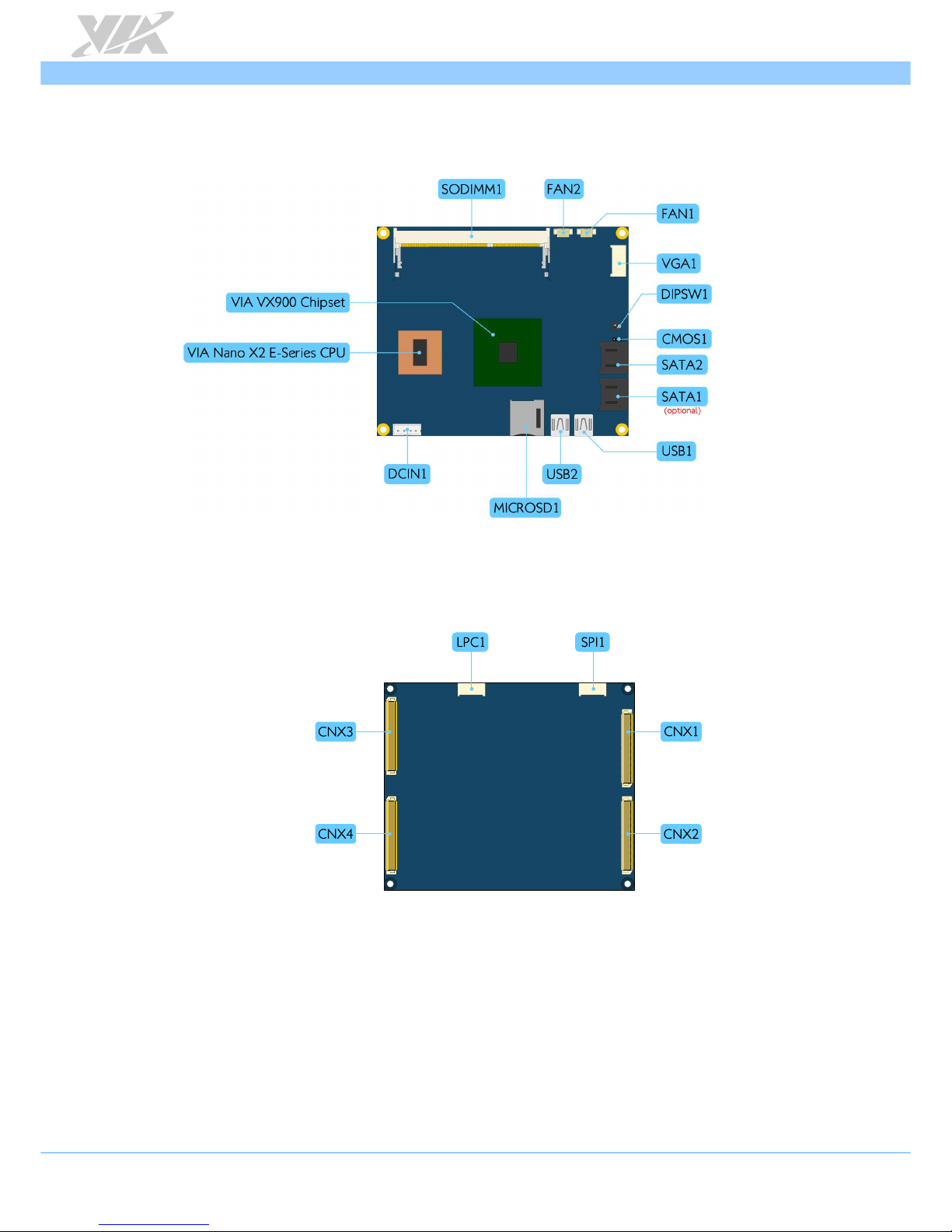
1.3. Layout Diagram
Figure 1: Layout diagram of the VIA ETX-8X90 module (top side)
Figure 2: Layout diagram of the VIA ETX-8X90 module (bottom side)
Page 14
VIA ETX-8X90 User Manual
5
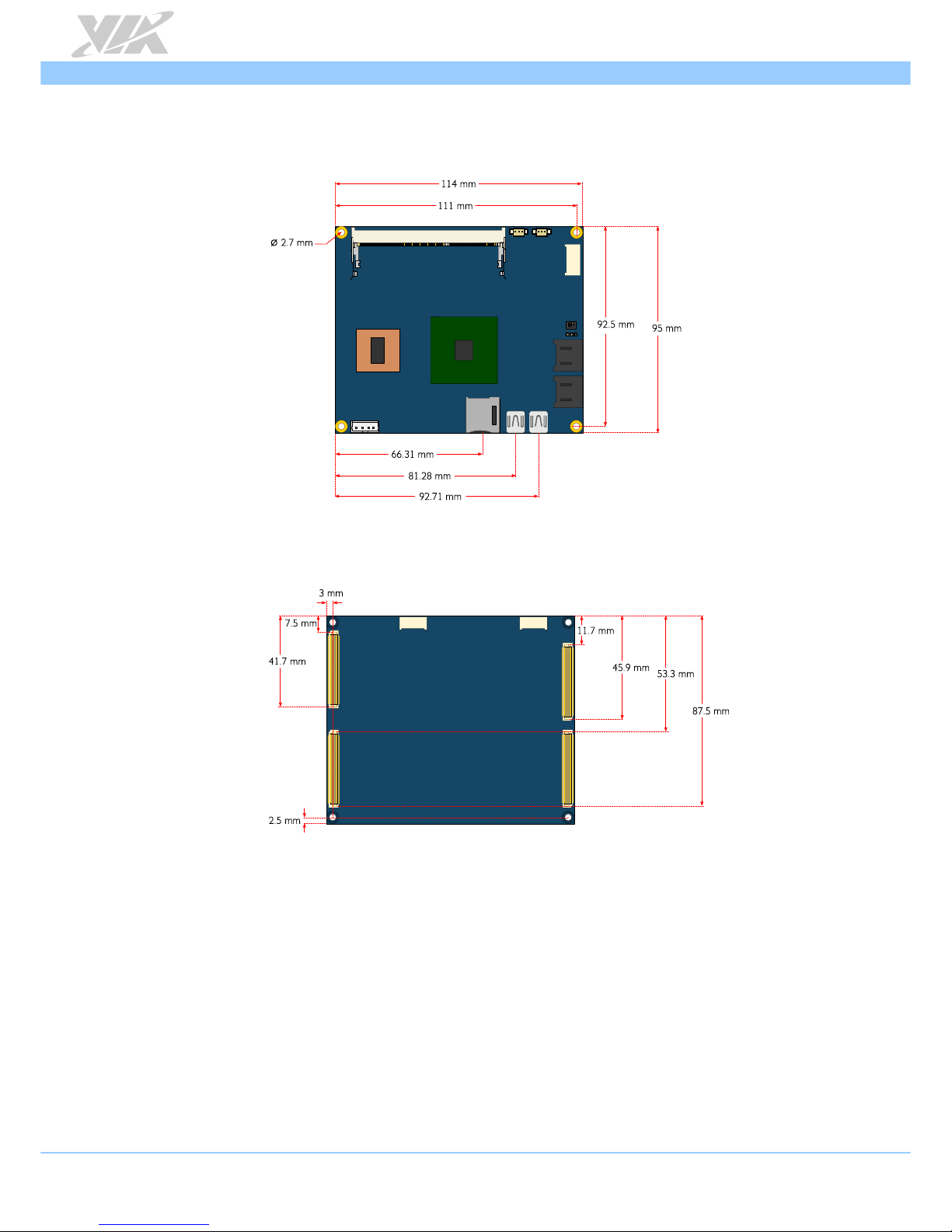
1.4. Product Dimensions
Figure 3: Dimensions of the VIA ETX-8X90 module (top view)
Figure 4: Dimensions of the VIA ETX-8X90 module (bottom view)
Page 15
VIA ETX-8X90 User Manual
6
2. I/O Interface
This chapter provides information about the VIA ETX-8X90’s onboard I/O connector and its functionality.
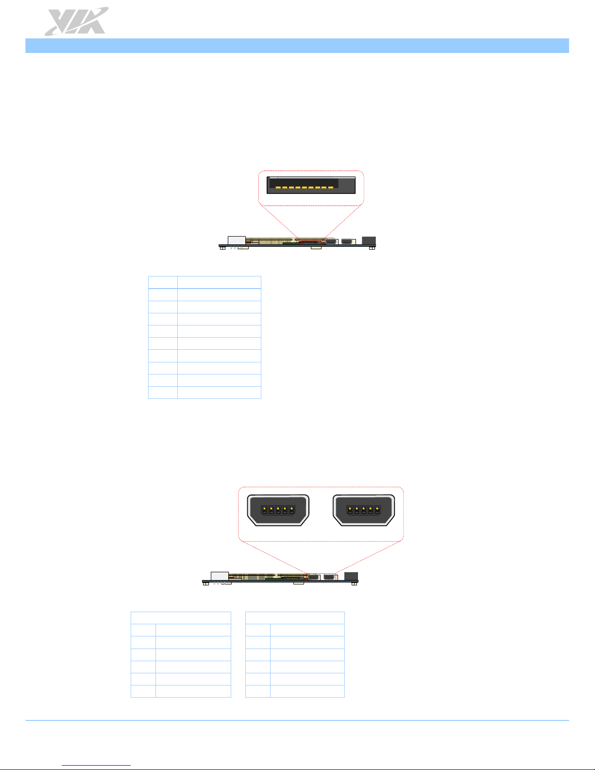
2.1. Micro SD Card Slot
The Micro SD card slot is for flash memory micro SD card that can provide additional storage data. The
Micro SD card slot can also be used for operating system booting for Window CE, Linux and VxWorks.
The pinouts of the Micro SD card slot are shown below.
1
9
MICROSD1
Figure 5: Micro SD card slot diagram
Pin Signal
1 CR_D2
2 CR_D3
3 CR_CMD
4 VCCCRPWR
5 CR_CLK
6 GND
7 CR_D0
8 CR_D1
9 -CR_CD
Table 1: Micro SD card slot pinouts
2.2. Mini USB 2.0 Ports
There are two integrated mini USB 2.0 ports on VIA ETX-8X90 module labeled as “USB1 and USB2”. The
mini USB port gives complete plug and play and hot swap capability for external devices. Each port is
using the USB mini-AB type receptacle connector. The pinouts of the mini USB 2.0 ports are shown below.
1
5
1
5
USB2 USB1
Figure 6: Mini USB 2.0 ports diagram
Mini USB port 1
Mini USB port 2
Pin Signal Pin Signal
1 +5VSUS 1 +5VSUS
2 USB4- 2 USB53 USB4+ 3 USB5+
4 GND 4 GND
5 GND 5 GND
Table 2: Mini USB 2.0 ports pinouts
Page 16
VIA ETX-8X90 User Manual
7
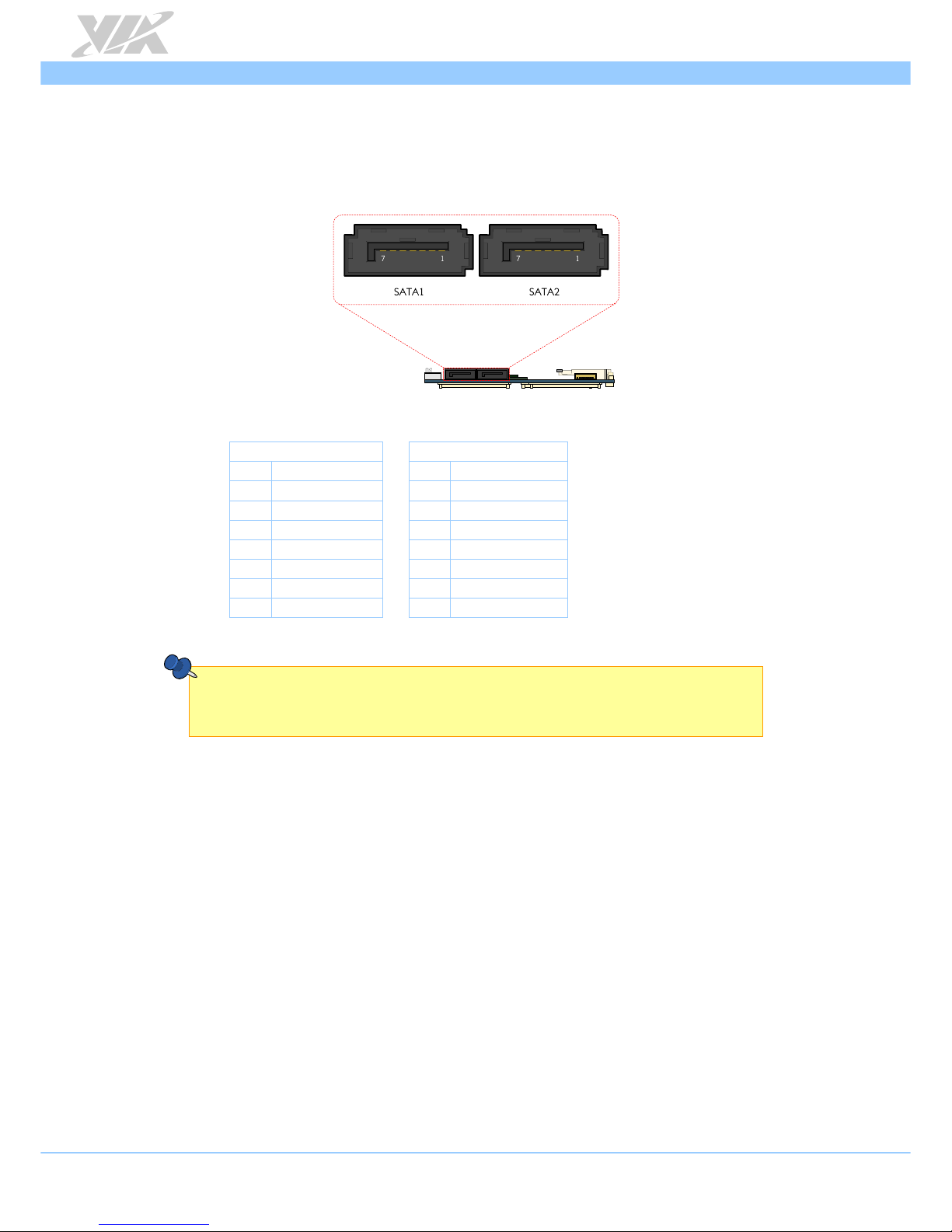
2.3. SATA Connectors
The two SATA connectors labeled as SATA1 (optional) and SATA21 on board can support up to 3.0Gbps
transfer speeds. Both connectors have 7th pin that can provide +5V power to a SATA Disk-On-Module
(DOM)2. When a regular SATA hard drive is connected, the 7th pin will be a ground pin. The pinouts of
the SATA connectors are shown below.
Figure 7: SATA connectors diagram
SATA1 connector
SATA2 connector
Pin Signal Pin Signal
1 GND 1 GND
2 STXP_0 2 STXP_1
3 STXN_0 3 STXN_1
4 GND 4 GND
5 SRXN_0 5 SRXN_1
6 SRXP_0 6 SRXP_1
7 GND 7 GND
Table 3: SATA connectors pinouts
Notes:
1. As default, SATA2 connector is enabled and SATA1 connector is disabled. The SATA1 connector is
a manufacturing option.
2. The SATA connector pin 7 default setting is GND. The +5V supports is a factory option.
Page 17
VIA ETX-8X90 User Manual
8
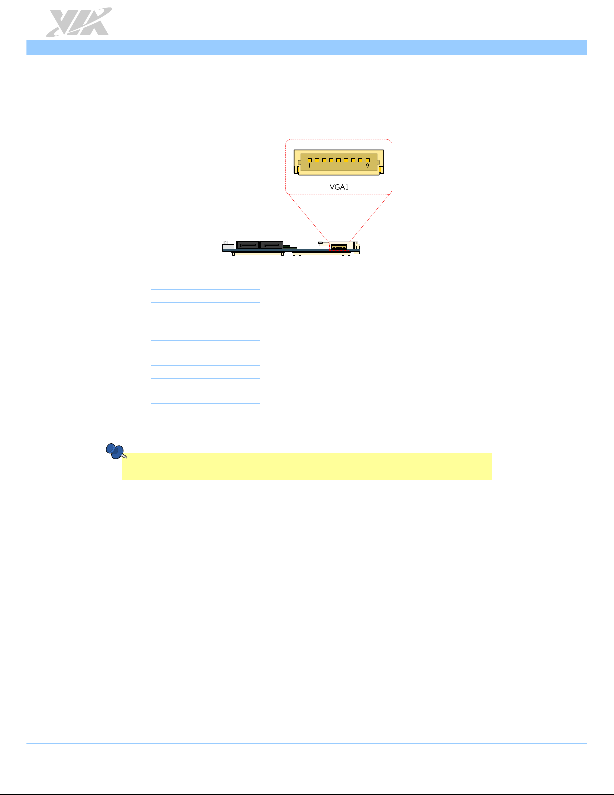
2.4. VGA Connector
The VIA ETX-8X90 module has on board VGA connector labeled as VGA1. This connector is for
connecting the VGA DE-15 connector to support high resolution analog VGA monitor. It supports up to
2048 x 1536 resolutions. The pinouts of the VGA connector are shown below.
Figure 8: VGA connector diagram
Pin Signal
1 REDN
2 GREENN
3 BLUEN
4 GND
5 HS
6 VS
7 GND
8 DDCCLKN
9 DDCDATAN
Table 4: VGA connector pinouts
Note:
The VGA1 connector is not for production used. It is reserved for debugging purposes only.
Page 18
VIA ETX-8X90 User Manual
9
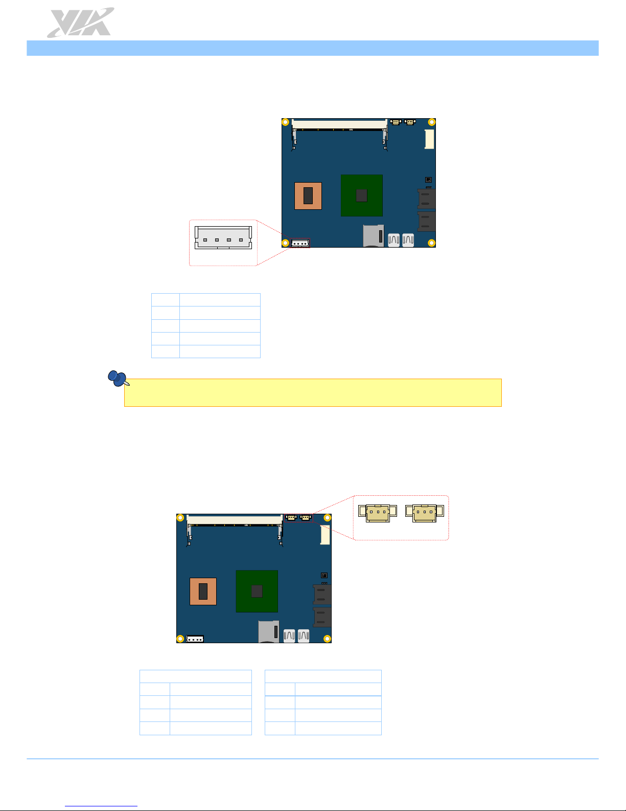
2.5. DC-in Connector
The VIA ETX-8X90 module has an onboard +5V DC-in 4-pin power connector to connect the DC-in power
cable. The DC-in connector is labeled as “DCIN1”. The pinouts of the DC-in connector are shown below.
DCIN1
1
Figure 9: DC-in connector diagram
Pin Signal
1 +5VSB
2 +5VSB
3 GND
4 GND
Table 5: DC-in connector pinouts
Note:
The DCIN1 connector is not for production used. It is reserved for debugging purposes only.
2.6. CPU and System Fan Connectors
There are two fan connectors on the module runs on +5V for maintaining CPU and System cooling. The
fan connector for the CPU is labeled as “FAN1” and the fan connector for the System is labeled as “FAN2”.
The fans provide variable speeds controlled by the BIOS. The fans can be forced to operate at full speed
by disabling the Smart Fan feature in the BIOS. The pinouts of the fan connectors are shown below.
FAN1
1
1
FAN2
Figure 10: CPU and System fan connectors diagram
CPU fan (FAN1)
System fan (FAN2)
Pin Signal Pin Signal
1 FANIN1 1 FANIN2
2 FANCTL1 (+5V) 2 FANCTL2 (+5V)
3 GND 3 GND
Table 6: CPU and System fan connectors pinouts
Page 19
VIA ETX-8X90 User Manual
10
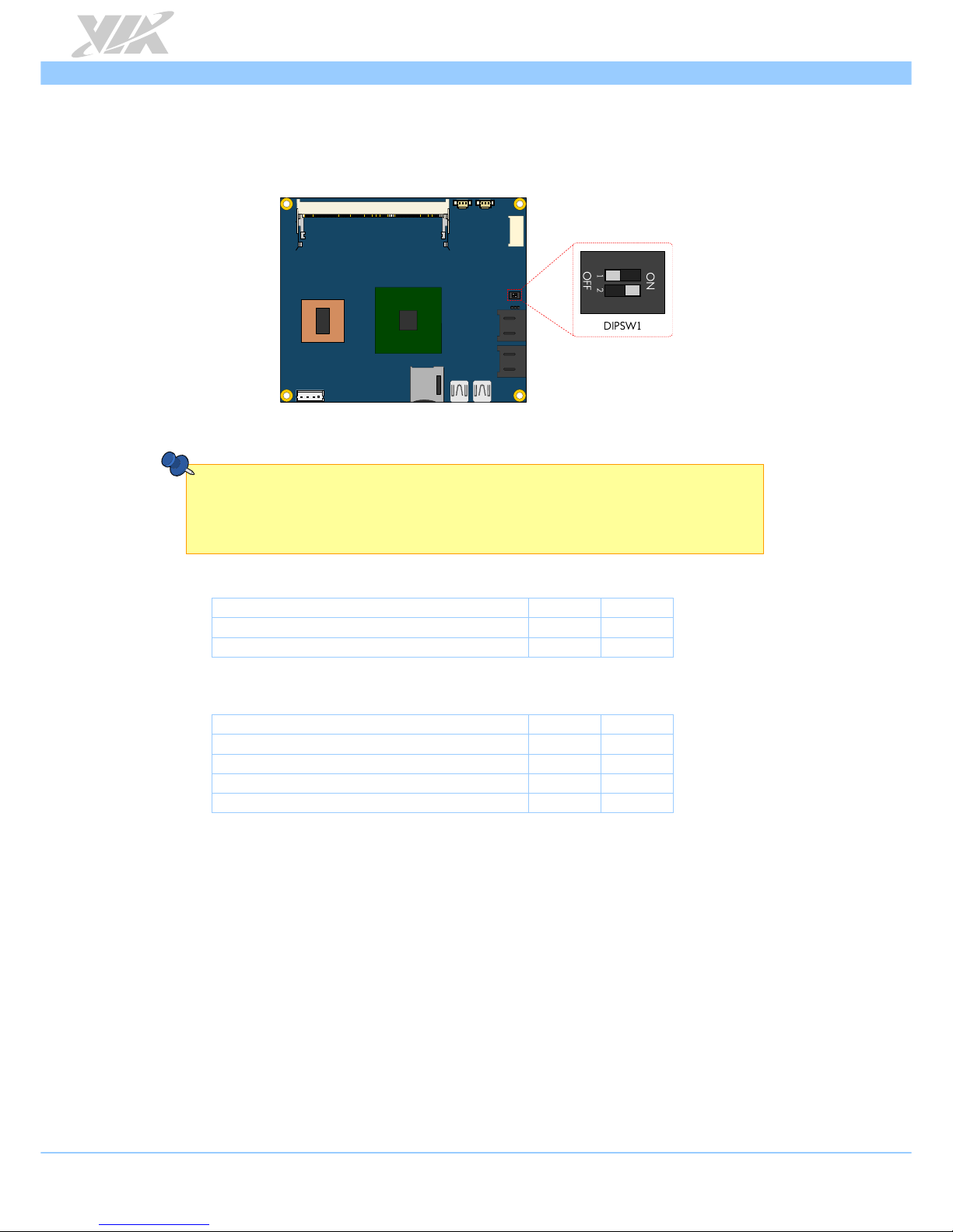
2.7. HDD Selector Switch
The VIA ETX-8X90 module has an onboard HDD selector DIP switch. The DIP switch is designed to
enable or disable the IDE HDD connector. The DIP switch is labeled as DIPSW1.
Figure 11: HDD selector DIP switch diagram
Notes:
1. The VIA ETX-8X90 only supports two channel of storage. The IDE1 + SATA2 configuration is the default
setting. The other configurations such as IDE1 + IDE2 (option 1) or SATA1 + SATA2 (option 2) are
manufacturing options.
2. The HDD Selector Switch (DIPSW1) is not applicable to SATA HDD configuration.
IDE1 + SATA2 HDD settings Switch 1 Switch 2
IDE1 HDD not install On N/A
IDE1 HDD install Off N/A
Table 7: IDE1 and SATA2 HDD configuration (default setting)
IDE1 + IDE2 HDD settings Switch 1 Switch 2
IDE1 and IDE2 HDD not install On On
IDE1 HDD not install and IDE2 HDD install On Off
IDE1 HDD install and IDE2 HDD not install Off On
IDE1 and IDE2 HDD install Off Off
Table 8: IDE1 and IDE2 HDD configuration (manufacturing option 1)
Page 20
VIA ETX-8X90 User Manual
11
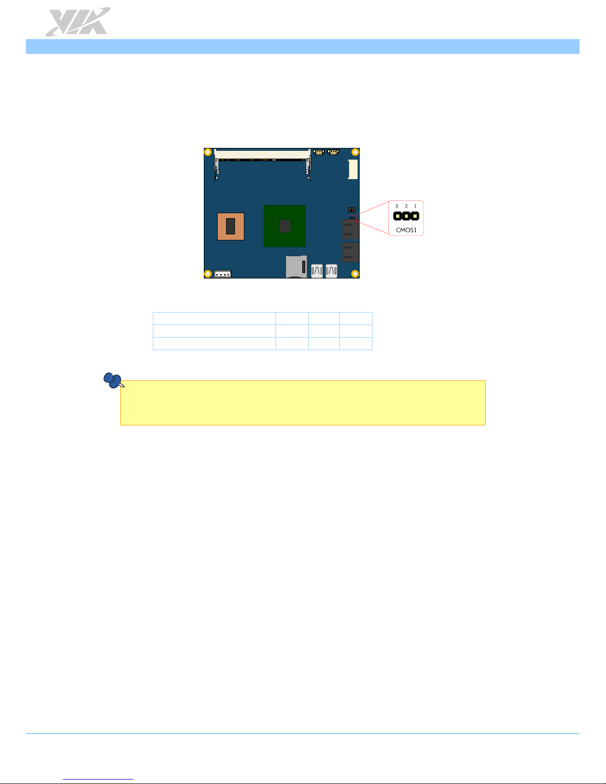
2.8. Clear CMOS Jumper
The onboard CMOS RAM stores system configuration data and has an onboard battery power supply. To
reset the CMOS settings, set the jumper on pins 2 and 3 while the system is off, and then return the
jumper to pins 1 and 2 afterwards. Setting the jumper while the system is on will damage the board. The
default setting is on pins 1 and 2.
Figure 12: Clear CMOS jumper diagram
Setting Pin 1 Pin 2 Pin 3
Normal (default setting) Short Short Open
Clear CMOS Open Short Short
Table 9: Clear CMOS jumper settings
Note:
Except when clearing the RTC RAM, never remove the cap from the CLEAR_CMOS jumper default position.
Removing the cap will cause system boot failure. Avoid clearing the CMOS while the system is on; it will
damage the board.
Page 21

VIA ETX-8X90 User Manual
12
2.9. LPC Connector
The VIA ETX-8X90 module has one LPC connector labeled as LPC1. The LPC connector can be used for
debugging purposes. The pinouts of the LPC connector are shown below..
Figure 13: LPC connector diagram
Pin Signal
1 +3.3V
2 -LPCRST
3 PCICLK1
4 LAD0
5 -LFRAME
6 LAD1
7 LAD3
8 LAD2
9 GND
Table 10: LPC connector pinouts
Note:
The LPC1 connector is not for production used. It is reserved for debugging purposes only.
Page 22

VIA ETX-8X90 User Manual
13
2.10. SPI Connector
The VIA ETX-8X90 module has one SPI flash connector. The SPI (Serial Peripheral Interface) flash
connector is used to connect the SPI BIOS programming fixture for updating the SPI flash ROM or for
debugging purposes. The SPI flash connector is labeled as “SPI1”. The pinouts of the SPI connector are
shown below.
Figure 14: SPI connector diagram
Pin Signal
1 NC
2 NC
3 MSPIDO
4 MSPIDI
5 MSPICLK
6 MSPISS0
7 GND
8 SPIVCC
Table 11: SPI connector pinouts
Note:
The SPI1 connector is not for production used. It is reserved for debugging purposes only.
Page 23
VIA ETX-8X90 User Manual
14
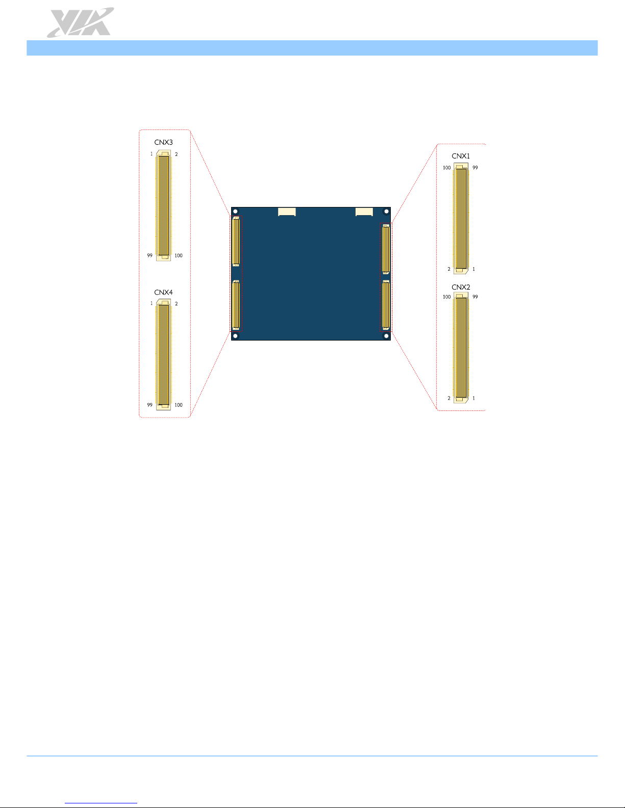
2.11. ETX Connectors
The VIA ETX-8X90 module has four ETX connectors labeled as “CNX1, CNX2, CNX3 and CNX4”. These
connectors are designed to provide interface to the carrier board.
Figure 15: ETX connectors diagram
Page 24

VIA ETX-8X90 User Manual
15
2.11.1. ETX Connector X1 (CNX1)
The ETX connector X1 contains signal groups of PCI bus, USB and Audio interface. The pinouts of the
connector X1 are shown below.
CNX1
Pin Signal Pin Signal Pin Signal Pin Signal
1 GND 2 GND 51 +5V 52 +5V
3 PCICLK_3 4 PCICLK_4 53 PAR 54 -SERR
5 GND 6 GND 55 -PERR 56 NC
7 PCLK1 8 PCLK2 57 -PME 58 USB2-
9 -REQ3_ETX 10 -GNT3_ETX 59 -PLOCK 60 -DEVSEL
11 GNT2_ETX 12 +3.3V 61 -TRDY 62 USB313 REQ2_ETX 14 -GNT1_ETX 63 -IRDY 64 -STOP
15 REQ1_ETX 16 +3.3V 65 -FRAME 66 USB2+
17 -GNT0_ETX 18 NC 67 GND 68 GND
19 +5V 20 +5V 69 AD16 70 -CBE2
21 SERIRQ1 22 -REQ0_ETX 71 AD17 72 USB3+
23 AD0 24 +3.3V 73 AD19 74 AD18
25 AD1 26 AD2 75 AD20 76 USB027 AD4 28 AD3 77 AD22 78 AD21
29 AD6 30 AD5 79 AD23 80 USB131 -CBE0 32 AD7 81 AD24 82 -CBE3
33 AD8 34 AD9 83 +5V 84 +5V
35 GND 36 GND 85 AD25 86 AD26
37 AD10 38 AUXAL 87 AD28 88 USB0+
39 AD11 40 MIC 89 AD27 90 AD29
41 AD12 42 AUXAR 91 AD30 92 USB1+
43 AD13 44 ASVCC 93 -PCIRST 94 AD31
45 AD14 46 SNDL 95 -INTC 96 -INTD
47 AD15 48 ASGND 97 -INTA 98 -INTB
49 -CBE1 50 SNDR 99 GND 100 GND
Table 12: ETX connector X1 pinouts
Page 25

VIA ETX-8X90 User Manual
16
2.11.2. ETX Connector X2 (CNX2)
The ETX connector X2 contains signal group of ISA bus interface. The pinouts of the connector X2 are
shown below.
CNX2
Pin Signal Pin Signal Pin Signal Pin Signal
1 GND 2 GND 51 +5V 52 +5V
3 SD14 4 SD15 53 SA6 54 IRQ5
5 SD13 6 -MASTER 55 SA7 56 IRQ6
7 SD12 8 DREQ7 57 SA8 58 IRQ7
9 SD11 10 -DACK7 59 SA9 60 SYS_CLK
11 SD10 12 DREQ6 61 SA10 62 -REFRESH
13 SD9 14 -DACK6 63 SA11 64 DREQ1
15 SD8 16 DREQ5 65 SA12 66 -DACK1
17 -MEMW 18 -DACK5 67 GND 68 GND
19 -MEMR 20 DREQ0 69 SA13 70 DREQ3
21 LA17 22 -DACK0 71 SA14 72 -DACK3
23 LA18 24 ISA_IRQ14 73 SA15 74 -IOR
25 LA19 26 ISA_IRQ15 75 SA16 76 -IOW
27 LA20 28 IRQ12 77 SA18 78 SA17
29 LA21 30 IRQ11 79 SA19 80 -SMEMR
31 LA22 32 IRQ10 81 -IOCHRDY 82 AEN
33 LA23 34 -IOCS16 83 +5V 84 +5V
35 GND 36 GND 85 SD0 86 -SMEMW
37 -SBHE 38 -MEMCSI6 87 SD2 88 SD1
39 SA0 40 ISA_OSC 89 SD3 90 -0WS
41 SA1 42 BALE 91 DREQ2 92 SD4
43 SA2 44 TC 93 SD5 94 IRQ9
45 SA3 46 -DACK2 95 SD6 96 SD7
47 SA4 48 IRQ3 97 -IOCHCK 98 -RSTDRV
49 SA5 50 IRQ4 99 GND 100 GND
Table 13: ETX connector X2 pinouts
Page 26

VIA ETX-8X90 User Manual
17
2.11.3. ETX Connector X3 (CNX3)
The ETX connector X3 contains signal groups of VGA, LCD, Video, COM, LPT and PS2 interfaces. The
pinouts of the connector X3 are shown below.
CNX3
Pin Signal Pin Signal Pin Signal Pin Signal
1 GND 2 GND 51 NC 52 NC
3 REDN 4 BLUEN 53 +5V 54 GND
5 HS 6 GREENN 55 P_-STB 56 P_-AFD
7 VS 8 DDCCLKN 57 NC 58 P_PRD7
9 NC 10 DDCDATAN 59 IRRX 60 P_-ERR
11 LVDSCLK2- 12 LVDSD7- 61 IRTX 62 P_PRD6
13 LVDSCLK2+ 14 LVDSD7+ 63 SIN2 64 P_-INIT
15 GND 16 GND 65 GND 66 GND
17 LVDSD5+ 18 LVDSD6+ 67 -RTS2 68 P_PRD5
19 LVDSD5- 20 LVDSD6- 69 -DTR2 70 P_-SLIN
21 GND 22 GND 71 -DCD2 72 P_PRD4
23 LVDSD3- 24 LVDSD4+ 73 -DSR2 74 P_PRD3
25 LVDSD3+ 26 LVDSD4- 75 -CTS2 76 P_PRD2
27 GND 28 GND 77 SOUT2 78 P_PRD1
29 LVDSD2- 30 LVDSCLK1+ 79 -RI2 80 P_PRD0
31 LVDSD2+ 32 LVDSCLK1- 81 +5V 82 +5V
33 GND 34 GND 83 SIN1 84 P_-ACK
35 LVDSD0+ 36 LVDSD1+ 85 -RTS1 86 P_BUSY
37 LVDSD0- 38 LVDSD1- 87 -DTR1 88 P_PE
39 +5V 40 +5V 89 -DCD1 90 P_SLCT
41 JILI_DAT 42 NC 91 -DSR1 92 MSCK
43 JILI_CLK 44 BLON 93 -CTS1 94 MSDT
45 BIASON 46 DIGON 95 SOUT1 96 KBCK
47 NC 48 NC 97 -RI1 98 KBDT
49 NC 50 NC 99 GND 100 GND
Table 14: ETX connector X3 pinouts
Page 27

VIA ETX-8X90 User Manual
18
2.11.4. ETX Connector X4 (CNX4)
The ETX connector X4 contains signal groups of IDE, Ethernet and Miscellaneous signal interfaces. The
pinouts of the connector X4 are shown below.
CNX4
Pin Signal Pin Signal Pin Signal Pin Signal
1 GND 2 GND 51 -SDIOW 52 -PDIOR
3 +5VSB 4 PWRGIN 53 SDDREQ 54 -PDIOW
5 PS_ON- 6 SPEAK_BZ 55 SDD15 56 PDDREQ
7 PW_BN- 8 +3.3VBAT 57 SDD0 58 PDD15
9 NC 10 LILED- 59 SDD14 60 PDD0
11 RSMRST- 12 ACTLED- 61 SDD1 62 PDD14
13 NC 14 SPEEDLED- 63 SDD13 64 PDD1
15 NC 16 I²C_CLK 65 GND 66 GND
17 +5V 18 +5V 67 SDD2 68 PDD13
19 OVCR- 20 NC 69 SDD12 70 PDD2
21 -EXTSMI 22 I²C_DAT 71 SDD3 72 PDD12
23 SMBCLK 24 SMBDATA 73 SDD11 74 PDD3
25 -SDCS3 26 -SMBALRT 75 SDD4 76 PDD11
27 -SDCS1 28 -HD_LED 77 SDD10 78 PDD4
29 SDA2 30 -PDCS3 79 SDD5 80 PDD10
31 SDA0 32 -PDCS1 81 +5V 82 +5V
33 GND 34 GND 83 SDD9 84 PDD5
35 SPDIG 36 PDA2 85 SDD6 86 PDD9
37 SDA1 38 PDA0 87 SDD8 88 PDD6
39 IRQ15 40 PDA1 89 GPE2- 90 PPDIG
41 -BATLOW 42 GPE1- 91 LAN_RXD- 92 PDD8
43 -SDDACK 44 IRQ14 93 LAN_RXD+ 94 SDD7
45 SIORDY 46 -PDDACK 95 LAN_TXD- 96 PDD7
47 -SDIOR 48 PIORDY 97 LAN_TXD+ 98 -HDRST
49 +5V 50 +5V 99 GND 100 GND
Table 15: ETX connector X4 pinouts
Page 28

VIA ETX-8X90 User Manual
19
3. Hardware Installation
3.1. Mounting VIA ETX-8X90 module onto the ETXDB1
carrier board
Step 1
Align the four ETX connectors and mounting holes of the VIA ETX-8X90 module into the ETX connectors
and mounting holes on the ETXDB1 carrier board.
Figure 16: Carrier board ETX connectors and mounting holes
Step 2
Gently press down the VIA ETX-8X90 module until the four ETX connectors have been fully inserted into
the ETX connectors on the ETXDB1 carrier board.
Figure 17: Installing the VIA ETX-8X90 module on the carrier board
Page 29

VIA ETX-8X90 User Manual
20
Step 3
Align the notch on the memory module with its counterpart on the SODIMM slot, and then insert the
memory module at a 30° angle.
Figure 18: Installing the DDR3 SODIMM memory module
Step 4
Push down until the memory module snaps into place. The memory slot has two locking mechanisms that
will click once the memory module has been fully inserted.
Step 5
Flip over the heatsink/heat spreader. Remove the plastic cover of the thermal pad of the memory and
chipset.
Figure 19: Removing the thermal pad cover
Page 30

VIA ETX-8X90 User Manual
21
Step 6
Apply the thermal grease/paste onto the surface of the CPU. Then align the heatsink/heat spreader over
the mounting holes on the VIA ETX-8X90 module.
Figure 20: Heatsink/heat spreader’s mounting holes on VIA ETX-8X90 module
Step 7
Gently install the heatsink/heat spreader. Make sure to install it in proper orientation. The thermal pads
underneath the heatsink/heat spreader should position above the memory and chipset respectively.
Figure 21: Installing the heatsink/heat spreader on VIA ETX-8X90 module
Page 31

VIA ETX-8X90 User Manual
22
Step 8
Connect the CPU fan jack to the fan connector (FAN1).
Step 9
Secure the VIA ETX-8X90 module with the heatsink/heat spreader by screwing and tightening four
M2.5*12 screws in sequence (torque is 2.5~2.6 kgfcm).
Note:
Be sure to follow the sequence shown below when tightening the screws, otherwise it may cause damage to
the device.
ETXDB1
ETXDB1
Side View
M2.5*12 screw
Top View
1
3
4
2
Figure 22: Securing the heatsink/heat spreader and VIA ETX-8X90 module
Page 32

VIA ETX-8X90 User Manual
23
4. BIOS Setup Utility
4.1. Entering the BIOS Setup Utility
Power on the computer and press
Delete
during the beginning of the boot sequence to enter the BIOS
Setup Utility. If the entry point has passed, restart the system and try again.
4.2. Control Keys
Up
Move up one row
Down
Move down one row
Left
Move to the left in the navigation bar
Right
Move to the right in the navigation bar
Enter
Access the highlighted item / Select the item
Esc
Jumps to the Exit screen or returns to the previous screen
Page up / +
1
Increase the numeric value
Page down / -
1
Decrease the numeric value
F1
General help2
F10
Save all the changes and exit
Notes:
1. Must be pressed using the 10-key pad.
2. The General help contents are only for the Status Page and Option Page setup menus.
4.3. Navigating the BIOS Menus
The main menu displays all the BIOS setup categories. Use the <
Left
>/<
Right
> and <Up>/<
Down
> arrow
keys to select any item or sub-menu. Descriptions of the selected/highlighted category are displayed at
the bottom of the screen.
The small triangular arrowhead symbol next to a field indicates that a sub-menu is available (see figure
below). Press <
Enter
> to display the sub-menu. To exit the sub-menu, press <
Esc
>.
4.4. Getting Help
The BIOS Setup Utility provides a “
General Help
” screen. This screen can be accessed at any time by
pressing F1. The help screen displays the keys for using and navigating the BIOS Setup Utility. Press
Esc
to
exit the help screen.
Page 33

VIA ETX-8X90 User Manual
24
4.5. System Overview
The System Overview screen is the default screen that is shown when the BIOS Setup Utility is launched.
This screen can be accessed by traversing the navigation bar to the “Main” label.
Figure 23: Illustration of the Main menu screen
4.5.1. AMIBIOS
The content in this section of the screen shows the current BIOS version, build date, and ID number.
4.5.2. Processor
This content in this section shows the CPU information that has been detected.
4.5.3. System Memory
This section shows the amount of available memory that has been detected.
4.5.4. System Time
This section shows the current system time. Press
Tab
to traverse right and
Shift+Tab
to traverse left
through the hour, minute, and second segments. The + and - keys on the number pad can be used to
change the values. The time format is [Hour : Minute : Second].
4.5.5. System Date
This section shows the current system date. Press
Tab
to traverse right and
Shift+Tab
to traverse left
through the month, day, and year segments. The + and - keys on the number pad can be used to change
the values. The weekday name is automatically updated when the date is altered. The date format is
[Weekday, Month, Day, Year].
Page 34

VIA ETX-8X90 User Manual
25
4.6. Advanced Settings
The Advanced Settings screen shows a list of categories that can provide access to a sub-screen. Subscreen links can be identified by the preceding right-facing arrowhead.
Figure 24: Illustration of the Advanced Settings screen
The Advanced Settings screen contains the following links:
• CPU Configuration
• SATA Configuration
• SuperIO Configuration
• Hardware Health Configuration
• ACPI Configuration
• APM Configuration
• Spread Spectrum Configuration
• USB Configuration
• CRB Configuration
Page 35

VIA ETX-8X90 User Manual
26
4.6.1. CPU Configuration
The CPU Configuration screen shows detailed information about the built-in processor.
Figure 25: Illustration of the CPU Configuration screen
4.6.2. SATA Configuration
The SATA Configuration screen shows links to the primary and secondary IDE hard drive information
screens.
Figure 26: Illustration of SATA Configuration screen
Page 36

VIA ETX-8X90 User Manual
27
4.6.2.1. Hard Disk Information
When a hard drive is detected, the hard drive’s detailed information can be displayed on the SATA-1
Primary/Secondary IDE sub-screen.
Figure 27: Illustration of SATA-1 Primary IDE screen
In addition, the PIO and DMA modes may be configured for each SATA hard drive.
4.6.2.1.1. PIO Mode
The PIO Mode has six possible settings: Auto, 0, 1, 2, 3, and 4. The “Auto” setting enables the BIOS to
autonomously determine the appropriate PIO mode for the hard drive. If a manual setting is preferred,
then be sure the correct PIO mode of the hard drive is used. It is not recommended to set the PIO mode
higher than what the hard drive manufacturer states.
4.6.2.1.2. DMA Mode
The DMA Mode has four possible settings: Auto, SWDMAn, MWDMAn and UDMAn. If a manual setting is
preferred, then be sure the correct DMA mode of the hard drive is used.
Auto
The “Auto” setting enables the BIOS to automatically detect DMA mode.
SWDMAn
Single Word DMA mode.
MWDMAn
Multi Word DMA mode.
UDMAn
Ultra DMA mode.
Page 37

VIA ETX-8X90 User Manual
28
4.6.3. SuperIO Configuration
The SuperIO Configuration screen shows the specific addresses, IRQs and types of the onboard serial
ports.
Figure 28: Illustration of SuperIO Configuration screen
4.6.3.1. Serial Ports 1 to 2 Address and IRQ
This option allows the user to select the Serial Port 1 and 2 base I/O address and interrupt request
address. The Serial Port 1 to 2 has selectable options.
Port Address IRQs
1 3F8, Disabled IRQ3, IRQ4, IRQ10, IRQ11
2 2F8, Disabled IRQ3, IRQ4, IRQ10, IRQ11
Table 16: Serial port addresses and IRQs
4.6.3.2. Serial Port 2 Mode
This specifies the serial port mode. The serial port mode has three options: Normal, IrDA (1.6 µs) and
IrDA (3/16 bit)
4.6.3.3. Parallel Port Address
This specifies the I/O port address and IRQ of the parallel port. The parallel port has four options:
Disabled and 378.
4.6.3.4. Parallel Port Mode
This specifies the parallel port mode. The parallel port mode has five options: Normal, Bi-Directional,
ECP, EPP, ECP+EPP.
4.6.3.5. Parallel Port IRQ
This specifies the parallel port interrupt request address. The parallel port IRQ has 2 options: IRQ5 and
IRQ7.
Page 38

VIA ETX-8X90 User Manual
29
4.6.4. Hardware Health Configuration
The Hardware Health Configuration screen displays the monitored aspects of the module such as CPU
temperature, system temperature, fan speeds, and voltages of the power planes.
Figure 29: Illustration of Hardware Health Configuration screen
4.6.4.1. Smart FAN 1 and FAN 2
The Smart FAN features have two options: Auto and Full Speed. The “Auto” option enables the BIOS to
adjust the fan speed according to the needs of the CPU and system. The “Full Speed” option forces the
fans to run at their maximum RPM.
Page 39

VIA ETX-8X90 User Manual
30
4.6.5. ACPI Configuration
ACPI grants the operating system direct control over system power management. The ACPI Configuration
screen can be used to set a number of power management related functions.
Figure 30: Illustration of ACPI Configuration screen
4.6.5.1. Suspend Mode
The Suspend Mode field has three selectable options.
S1(POS)
S1/Power On Suspend (POS) is a low power state. In this state, no system context (CPU or chipset) is lost
and hardware maintains all system contexts.
S3(STR)
S3/Suspend To RAM (STR) is a power-down state. In this state, power is supplied only to essential
components such as main memory and wakeup-capable devices. The system context is saved to main
memory, and context is restored from the memory when a "wakeup" event occurs.
Auto
When the Suspend Mode is set to Auto, the operating system will control the power state.
4.6.5.2. ACPI Version Features
The ACPI Version Features enables the BIOS to support the designated ACPI specification. There are three
versions to choose from: ACPI v1.0, ACPI v2.0, and ACPI v3.0.
Page 40

VIA ETX-8X90 User Manual
31
4.6.6. APM Configuration
APM enables the operating system to co-work with the BIOS to control the system power management.
The APM Configuration screen can be used to set a number of power management functions.
Figure 31: Illustration of APM Configuration screen
4.6.6.1. Power Button Mode
The Power Button Mode has three options.
On/Off
When On/Off is selected, pressing the power button will instantly cause the system to power on or off.
Standby
When Standby is selected, the power button must be pressed and held down for 4 seconds before the
system will power off.
Suspend
When Suspend is selected, pressing the power button will instantly cause the system to enter suspend
mode.
4.6.6.2. Restore on AC/Power Loss
Restore on AC/Power Loss defines how the system will respond after AC power has been interrupted
while the system is on. There are three options.
Power Off
The Power Off option keeps the system in an off state until the power button is pressed again.
Power On
The Power On option restarts the system when the power has returned.
Last State
The Last State option restores the system to its previous state when the power was interrupted.
4.6.6.3. Resume On PCI PME#
The Resume On PCI PME# feature has two settings: Enabled and Disabled. When the setting is changed to
“Enabled”, the system will boot if PME event is triggered via PCI devices. When the setting is changed to
“Disabled”, this feature will not be function.
Page 41

VIA ETX-8X90 User Manual
32
4.6.6.4. Resume On KBC
Resume on KBC wakes up a system that has been put into suspend or standby mode. When this feature is
enabled, keyboard activity as defined in the
Wake-Up Key
feature will cause the system to wake up. This
feature has three options.
S3
The S3 option enables keyboard activity to be detected if the system is in S3 power saving mode.
S3/S4/S5
The S3/S4/S5 option enables keyboard activity to be detected if the system is in S3/S4/S5 power saving
mode.
Disabled
The Disabled option disables the detection of all keyboard activity.
4.6.6.5. Wake-Up Key
The Wake-Up Key feature can only be set when
Resume on PS/2 KBC
is set to “S3” or “S3/S4/S5”.
Otherwise, this feature will be not selectable. This feature has two options.
Any Key
The Any Key option enables any key on the keyboard to trigger the Wake-Up event.
Specific Key
The Specific Key option unlocks the
Wake-Up Password
feature.
4.6.6.6. Wake-Up Password
The Wake-Up Password feature can only be set when the
Wake-Up Key
feature is set to “Specific Key”.
This feature enables the user to specify a key sequence that must be entered in order to wake up the
system.
The key sequence can consist of up to 6 alphanumeric characters and some special characters. Function
keys and modifier keys (such as Ctrl, Alt, Del, etc.) cannot be used.
4.6.6.7. Resume On PS/2 Mouse
Resume on PS/2 Mouse wakes up a system that has been put into suspend or standby mode. When this
feature is enabled, any PS/2 mouse activity that is detected will cause the system to wake up. This feature
has three options.
S3
The S3 option enables any PS/2 mouse activity to be detected if the system is in S3 power saving mode.
S3/S4/S5
The S3/S4/S5 option enables any PS/2 mouse activity to be detected if the system is in S3/S4/S5 power
saving mode.
Disabled
The Disabled option disables the detection of all PS/2 mouse activity.
4.6.6.8. Resume on RTC Alarm
This feature enables the BIOS to automatically power on the system at a scheduled time. When enabled,
the
RTC Alarm Date
and
System Time
features will be unlocked.
4.6.6.9. RTC Alarm Date (Days)
The RTC Alarm Date feature is visible only when
Resume on RTC Alarm
is enabled. This feature enables
the user to specify a specific date each month or daily recurrence. Use the + and - keys on the number
pad to change the value of the RTC Alarm Date.
Every Day
The Every Day option triggers the RTC Alarm daily.
1 – 31
When a specific numeric date is selected, the RTC Alarm will be triggered on that day of the month.
Page 42

VIA ETX-8X90 User Manual
33
4.6.6.10. System Time
The System Time option enables the user to specify the time the system should power on for the date
that is set in
RTC Alarm Date
.
4.6.7. Spread Spectrum Configuration
The Spread Spectrum Configuration screen enables access to the CPU Spread Spectrum Setting feature.
Figure 32: Illustration of Spread Spectrum Configuration screen
4.6.7.1. CPU Spread Spectrum Setting
The CPU Spread Spectrum Setting feature enables the BIOS to modulate the clock frequencies originating
from the module. The settings are in percentages of modulation. Higher percentages result in greater
modulation of clock frequencies. This feature has settings that range from 0.1% to 0.9%.
Page 43

VIA ETX-8X90 User Manual
34
4.6.8. USB Configuration
The USB Configuration screen shows the number of connected USB devices. Additionally, support for
various USB features can be enabled or disabled.
Figure 33: Illustration of USB Configuration screen
4.6.9. CRB Configuration
The CRB Configuration screen includes several chipset settings.
Figure 34: Illustration of CRB Configuration screen
Page 44

VIA ETX-8X90 User Manual
35
4.6.9.1. DRAM Clock
The DRAM Clock feature enables the user to determine how the BIOS handles the memory clock
frequency. The memory clock can either be dynamic or static. This feature has three options.
Auto
The Auto option enables the BIOS to select a compatible clock frequency for the installed memory.
400 MHz
The 400 MHz option forces the BIOS to be fixed at 800 MHz for DDR3 memory modules.
533 MHz
The 533 MHz option forces the BIOS to be fixed at 1066 MHz for DDR3 memory modules.
4.6.9.2. Select Display Device 1 and 2
The Select Display Device feature enables the user to choose a specific display interface. This feature has
two options: CRT and LCD.
4.6.9.3. Panel Type
This feature enables the user to specify the resolution of the display being used with the system. The
panel types are predefined in the VGA VBIOS.
Panel Type
Resolution Panel Type Resolution
00 640 x 480 08 800 x 480
01 800 x 600 09 1024 x 600
02 1024 x 768 10 1366 x 768
03 1280 x 768 11 1600 x 1200
04 1280 x 1024 12 1680 x 1050
05 1400 x 1050 13 User define
06 1440 x 900 14 User define
07 1280 x 800 15 User define
Table 17: Panel types resolution
4.6.9.4. VGA Share Memory (Frame Buffer)
The VGA Share Memory feature enables the user to choose the amount of the system memory to reserve
for use by the integrated graphics controller. The amount of memory options are: 128 MB, 256 MB and
512 MB.
4.6.9.5. OnChip HDAC Device
The OnChip HDAC Device feature enables the BIOS to control the high definition audio codec in the
chipset. This feature has two options: enable and disable.
4.6.9.6. SMBus Device Switch
This feature enables support for the new chipset definition of the SMBus interface. There are two options:
New SMBus Device and Old SMBus Device. If the OS cannot support the new SMBus definition, then
change the setting to “Old SMbus Device”.
4.6.9.7. SDIO Host controller
The SDIO Host controller feature has two options: Enabled and Disabled.
4.6.9.8. WATCH-DOG
The WATCHDOG Timer Enable feature unlocks two other features that enable the BIOS to monitor the
state of the system. This feature has two options: enabled or disabled.
4.6.9.9. Unit-Select
The Unit-Select feature is only available if the
WATCH-DOG
feature has been enabled. This feature has
two options: minutes and seconds.
Page 45

VIA ETX-8X90 User Manual
36
4.6.9.10. Time-Select
The Time-Select is only available if the
WATCH-DOG
feature has been enabled. This feature requires the
user to input an integer in the range of 0–255 if the
Unit-Select
feature is set to “Seconds”. If the
Unit-
Select
feature is set to “Minutes”, then the user can only input an integer in the range of 0–17. If the user
inputs “0”, the
WATCH-DOG
feature will be disabled regardless of the setting for
Unit-Select
.
4.6.9.11. Backlight Control
The Backlight Control feature enables the user to control the brightness of the LCD backlight. This feature
has four options.
Level 1
25% Light
Level 2
50% Light
Level 3
75% Light
Level 4
100% Light
4.6.9.12. Backlight PWM Clock
The Backlight PWM Clock feature enables the user to correct the LCD backlight PWM clock. This feature
has four options: 14 KHz, 7 KHz, 110 Hz, 54.4 Hz.
4.6.9.13. LAN Boot ROM
The LAN Option ROM feature has two options: Enabled and Disabled. If the LAN Boot ROM feature is
enabled, then the system will load a separate ROM for the LAN controller in order to boot through the
LAN Ethernet. When the setting is changed to “Disabled”, the system does not load a separate ROM from
the LAN controller.
Page 46

VIA ETX-8X90 User Manual
37
4.7. Boot Settings
The Boot Settings screen has two links that goes to the
Boot Settings Configuration
and
Boot Device
Priority
screens.
Figure 35: Illustration of Boot Settings screen
4.7.1. Boot Settings Configuration
The Boot Settings Configuration screen has several features that can be run during the system boot
sequence.
Figure 36: Illustration of Boot Settings Configuration screen
Page 47

VIA ETX-8X90 User Manual
38
4.7.1.1. Quick Boot
The Quick Boot feature enables the BIOS to skip certain tests in order to speed up the boot sequence.
This feature has two options: “Enabled” and “Disabled”.
4.7.1.2. Quiet Boot
The Quiet Boot feature hides all of the Power-on Self Test (POST) messages during the boot sequence.
Instead of the POST messages, the user will see an OEM logo. This feature has two options: enabled and
disabled.
4.7.1.3. Bootup Num-Lock
The Bootup Num-Lock feature determines how the 10-key pad will behave. When the feature is enabled,
the 10-key pad will behave as a number pad. When the feature is disabled, the 10-key pad will behave as
cursor navigation keys.
4.7.1.4. Wait for ‘F1’ if Error
This feature determines how the system will respond if an error is detected during the boot sequence. If
this feature is enabled, the BIOS will pause booting and wait for the user to press F1 to enter the BIOS
setup menu. This feature has two options: enabled and disabled.
4.7.1.5. Hit ‘DEL’ Message Display
This feature determines if the BIOS will display a POST message that informs the user how to access the
BIOS Setup Utility.1 This feature has two options: enabled and disabled.
Note:
1. If the Quiet Boot option is enabled, the settings of this feature will have no effect.
Page 48

VIA ETX-8X90 User Manual
39
4.7.2. Boot Device Priority
The Boot Device Priority screen lists all bootable devices.
Figure 37: Illustration of Boot Device Priority screen
4.7.2.1. 1st Boot Device
This feature specifies the boot sequence from the available devices. The available boot devices are
detected dynamically and bootable devices will be listed accordingly. This feature has two options:
Network: Realtek Boot Agent and Disabled]
Page 49

VIA ETX-8X90 User Manual
40
4.8. Security Settings
The Security Settings screen provides a way to restrict access to the BIOS or even the entire system.
Figure 38: Illustration of Security Settings screen
4.8.1. Change Supervisor Password
This option is for setting a password for accessing the BIOS setup utility. When a password has been set,
a password prompt will be displayed whenever the BIOS setup utility is launched. This prevents an
unauthorized person from changing any part of the system configuration.
When a supervisor password is set, the
Password Check
option will be unlocked.
4.8.2. User Access Level
This feature controls the level of access a user (without the supervisor password) is granted to the BIOS
setup utility. This feature has four options.
No Access
The No Access option completely locks the BIOS setup utility. The supervisor password is required to
access and change the BIOS settings.
View Only
The View Only option only allows access to view the BIOS settings. Users with this permission level
cannot make changes to the BIOS.
Limited
The Limited option only allows non-critical BIOS settings to be changed. Changes are allowed to the
following BIOS features:
System Time
System Date
Quick Boot
Display Logo
Full Access
The Full Access option allows all BIOS settings to be changed except for the Change Supervisor
Password and User Access Level options.
Page 50

VIA ETX-8X90 User Manual
41
4.8.3. Change User Password
This option is for setting a password for non-supervisors. When a user password is set, the
Clear User
Password
and
Password Check
options will be unlocked.
4.8.4. Clear User Password
This option is only available when the user accesses the BIOS Setup Utility when the user password has
been specified.
4.8.5. Password Check
This feature is compulsory when the
Change Supervisor Password
option is set. The user will have up to
three chances to enter the correct password before the BIOS forces the system to stop booting. If the user
does not enter the correct password, the keyboard will also lock up. The only way to get past this is to
do a hard reboot (i.e., use the system reset button or cut off the power to the system). A soft reboot (i.e.,
Ctrl+Alt+Del) will not work because the keyboard will be locked. This feature has two options.
Setup
The Setup option forces users to enter a password in order to access the BIOS Setup Utility.
Always
The Always option forces users to enter a password in order to boot up the system.
Page 51

VIA ETX-8X90 User Manual
42
4.9. Exit Options
Figure 39: Illustration of Exit Options screen
4.9.1. Save Changes and Exit
Save all changes to the BIOS and exit the BIOS Setup Utility. The “F10” hotkey can also be used to trigger
this command.
4.9.2. Discard Changes and Exit
Exit the BIOS Setup Utility without saving any changes. The “Esc” hotkey can also be used to trigger this
command.
4.9.3. Discard Changes
This command reverts all changes to the settings that were in place when the BIOS Setup Utility was
launched.
4.9.4. Load Optimal Defaults
Load optimal default values for all the setup items. The default optimized values are defined by the
board manufacturer to provide optimized environment for a basic system.
Page 52

VIA ETX-8X90 User Manual
43
5. Software and Technical Support
5.1. Microsoft and Linux Support
The VIA VIA ETX-8X90 module is highly compatible with Microsoft Windows and Linux operating systems.
5.1.1. Driver Installation
Microsoft Driver Support
The latest drivers can be downloaded from the VIA website at
www.viatech.com
Linux Driver Support
Linux drivers are provided through various methods including:
• Drivers provided by VIA
• Using a driver built into a distribution package
• Visiting
www.viatech.com
for the latest updated drivers
• Installing a third party driver (such as the ALSA driver from the Advanced Linux Sound
Architecture project for integrated audio)
5.2. Technical Support and Assistance
• For utilities downloads, latest documentation and new information about the VIA ETX-8X90,
please visit our website at
http://www.viatech.com/en/boards/modules/etx-8x90/
• For technical support and additional assistance, always contact your local sales representative or
board distributor, or go to
https://www.viatech.com/en/support/driver-support-faq/technical-
support/
for technical support.
• For OEM clients and system integrators developing a product for long term production, other
code and resources may also be made available. Please visit our website at
https://www.viatech.com/en/about/
to submit a request.
Page 53

VIA ETX-8X90 User Manual
44
Appendix A. ETXDB1 Carrier Board Reference
A.1. Board Specifications
Module Name
o ETXDB1
Rear I/O Connector
o 1 x VGA port
o 1 x COM port
o 4 x USB 2.0 ports
o 1 x 10/100Mbps Ethernet port
Onboard Connector and Slot
o 4 x ETX connectors
o 1 x ISA slot (compatible with ISA ETX 3.02)
o 2 x IDE connectors (IDE1 and IDE2)
o 2 x PCI slots (compatible with PCI 2.3, 32bit/33MHz)
o 1 x LVDS panel connector (compatible with TIA/ELA-644)
Pixel clock up to 85MHz
Support panel resolution up to WXGA 1366x768
Supports one or two-channel 18-bit or 24-bit LVDS panel
o 1 x Backlight connector
o 1 x ATX power connector
o 1 x RTC battery slot
Onboard Pin Header
o 1 x LPT pin header
o 1 x Keyboard and Mouse pin header
o 1 x COM pin header
o 1 x Front Panel pin header (for HDD LED, Power LED, Switch and Speaker)
o 1 x Front Audio pin header
o 1 x SMBus pin header
o 1 x I²C bus pin header
o 1 x SIR pin header
Onboard Jumper and Switch
o 1 x Backlight and Panel Power jumper
Onboard Speaker
o 1 x Buzzer speaker
Form Factor and Dimensions
o Mini-ITX
o 6 Layers
o 17cm x 17cm (6.7” x 6.7”)
Operating Temperature
o 0°C ~ 60°C
Operating and Storage Humidity
o 95% relative humidity
Page 54

VIA ETX-8X90 User Manual
45
A.1.1. Board Storage Channel Configuration
ETXDB1
(Carrier Board)
VIA ETX-8X90
(Computer-On-Module)
IDE1 IDE2 SATA1 SATA2
Default settings Enable Disable Disable Enable
Manufacturing option 1 Enable Enable Disable Disable
Manufacturing option 2 Disable Disable Enable Enable
Table 18: ETXDB1 and VIA ETX-8X90 storage configuration
Page 55

VIA ETX-8X90 User Manual
46
A.2. External I/O Connectors
The ETXDB1 has a wide selection of interfaces. It includes a selection of frequently used ports and
connectors as part of the external I/O coastline.
A.2.1. Rear I/O Ports
USB 2.0 ports
Ethernet port
VGA port
COM port
Figure 40: Rear I/O ports
Page 56

VIA ETX-8X90 User Manual
47
A.3. ETXDB1 Layout Diagram
A.3.1. Onboard Connectors and Slots
Figure 41: ETXDB1 connectors and slots diagram
Item Description
ISA1 ISA slot
IDE2 IDE connector 2
BUZZER1 Buzzer speaker
BAT1 RTC battery
CNX1 ETX connector X1
ATX1 20-pin ATX power connector
CNX2 ETX connector X2
CNX4 ETX connector X4
CNX3 ETX connector X3
BL1 Backlight connector
LVDS1 LVDS panel connector
PCI1 PCI slot 1
PCI2 PCI slot 2
IDE1 IDE connector 1
Table 19: Description table of the ETXDB1 connectors and slots
Page 57

VIA ETX-8X90 User Manual
48
A.3.2. Onboard Pin headers and Jumpers
Figure 42: ETXDB1 pin headers and jumpers diagram
Item Description
F_AUDIO1 Front audio pin header
I2C1 I2C pin header
SIR1 Serial Infrared pin header
SMB1 System Management Bus (SMBus) pin header
F_PANEL1 Front panel pin header
LPT1 Line Print Terminal pin header
COM2 COM pin header
KBMS2 Keyboard and mouse pin header
J1 Backlight voltage and panel power jumper
Table 20: Description table of the ETXDB1 pin headers and jumpers
Page 58

VIA ETX-8X90 User Manual
49
A.3.3. Connectors and Slots Pin Definition
A.3.3.1. ATX1 : 20-pin ATX Power Connector
Figure 43: ATX Power connector diagram
Pin Signal
1 +3.3V
2 +3.3V
3 GND
4 +5V
5 GND
6 +5V
7 GND
8 PW-OK
9 +5VSB
10 +12V
11 +3.3V
12 -12V
13 GND
14 PS-ON
15 GND
16 GND
17 GND
18 -5V
19 +5V
20 +5V
Table 21: ATX Power connector pinouts
Page 59

VIA ETX-8X90 User Manual
50
A.3.3.2. ISA1: ISA Slot
Figure 44: ISA slot diagram
Pin Signal Pin Signal Pin Signal Pin Signal
A1 -IOCHCK B1 GND C1 -SBHE D1 -MEMCS16
A2 SD7 B2 -RSTDRV C2 LA23 D2 -IOCS16
A3 SD6 B3 +5V C3 LA22 D3 IRQ10
A4 SD5 B4 IRQ9 C4 LA21 D4 IRQ11
A5 SD4 B5 -5V C5 LA20 D5 IRQ12
A6 SD3 B6 DREQ2 C6 LA19 D6 ISA_IRQ15
A7 SD2 B7 -12V C7 LA18 D7 ISA_IRQ14
A8 SD1 B8 -0WS C8 LA17 D8 -DACK0
A9 SD0 B9 +12V C9 -MEMR D9 DREQ0
A10 IOCHRDY B10 GND C10 -MEMW D10 -DACK5
A11 AEN B11 -SMEMW C11 SD8 D11 DREQ5
A12 SA19 B12 -SMEMR C12 SD9 D12 -DACK6
A13 SA18 B13 -IOW C13 SD10 D13 DREQ6
A14 SA17 B14 -IOR C14 SD11 D14 -DACK7
A15 SA16 B15 -DACK3 C15 SD12 D15 DREQ7
A16 SA15 B16 DREQ3 C16 SD13 D16 +5V
A17 SA14 B17 -DACK1 C17 SD14 D17 -MASTER
A18 SA13 B18 DREQ1 C18 SD15 D18 GND
A19 SA12 B19 -REFRESH
A20 SA11 B20 SYS_CLK
A21 SA10 B21 IRQ7
A22 SA9 B22 IRQ6
A23 SA8 B23 IRQ5
A24 SA7 B24 IRQ4
A25 SA6 B25 IRQ3
A26 SA5 B26 -DACK2
A27 SA4 B27 TC
A28 SA3 B28 BALE
A29 SA2 B29 +5V
A30 SA1 B30 ISA_OSC
A31 SA0 B31 GND
Table 22: ISA slot pinouts
Page 60

VIA ETX-8X90 User Manual
51
A.3.3.3. PCI1 and PCI2: PCI Slots
Figure 45: PCI slot diagram
PCI1
Pin Signal Pin Signal Pin Signal Pin Signal
A1 NC A2 +12V B1 -12V B2 NC
A3 NC A4 NC B3 GND B4 NC
A5 +5V A6 -INTA B5 +5V B6 +5V
A7 -INTC A8 +5V B7 -INTB B8 -INTD
A9 NC A10 +5V B9 NC B10 NC
A11 NC A12 GND B11 NC B12 GND
A13 GND A14 +3.3V AUX B13 GND B14 NC
A15 -PCIRST A16 +5V B15 GND B16 PCICLK1
A17 -GNT0 A18 GND B17 GND B18 -REQ0
A19 -PME A20 AD30 B19 +5V B20 AD31
A21 +3.3V A22 AD28 B21 AD29 B22 GND
A23 AD26 A24 GND B23 AD27 B24 AD25
A25 AD24 A26 IDSEL B25 +3.3V B26 -CBE3
A27 +3.3V A28 AD22 B27 AD23 B28 GND
A29 AD20 A30 GND B29 AD21 B30 AD19
A31 AD18 A32 AD16 B31 +3.3V B32 AD17
A33 +3.3V A34 -FRAME B33 -CBE2 B34 GND
A35 GND A36 -TRDY B35 -IRDY B36 +3.3V
A37 GND A38 -STOP B37 -DEVSEL B38 GND
A39 +3.3V A40 GND B39 -PLOCK B40 -PERR
A41 NC A42 GND B41 +3.3V B42 -SERR
A43 PAR A44 AD15 B43 +3.3V B44 -CBE1
A45 +3.3V A46 AD13 B45 AD14 B46 GND
A47 AD11 A48 GND B47 AD12 B48 AD10
A49 AD9 A50 - B49 GND B50 A51 - A52 -CBE0 B51 - B52 AD8
A53 +3.3V A54 AD6 B53 AD7 B54 +3.3V
A55 AD4 A56 GND B55 AD5 B56 AD3
A57 AD2 A58 AD0 B57 GND B58 AD1
A59 +5V A60 -P1REQ64 B59 +5V B60 -P1ACK64
A61 +5V A62 +5V B61 +5V B62 +5V
Table 23: PCI slot 1 pinouts
Page 61

VIA ETX-8X90 User Manual
52
PCI2
Pin Signal Pin Signal Pin Signal Pin Signal
A1 NC A2 +12V B1 -12V B2 NC
A3 NC A4 NC B3 GND B4 NC
A5 +5V A6 -INTB B5 +5V B6 +5V
A7 -INTD A8 +5V B7 -INTC B8 -INTA
A9 NC A10 +5V B9 NC B10 NC
A11 NC A12 GND B11 NC B12 GND
A13 GND A14 +3.3V AUX B13 GND B14 NC
A15 -PCIRST A16 +5V B15 GND B16 PCICLK2
A17 -GNT1 A18 GND B17 GND B18 -REQ1
A19 -PME A20 AD30 B19 +5V B20 AD31
A21 +3.3V A22 AD28 B21 AD29 B22 GND
A23 AD26 A24 GND B23 AD27 B24 AD25
A25 AD24 A26 IDSEL B25 +3.3V B26 -CBE3
A27 +3.3V A28 AD22 B27 AD23 B28 GND
A29 AD20 A30 GND B29 AD21 B30 AD19
A31 AD18 A32 AD16 B31 +3.3V B32 AD17
A33 +3.3V A34 -FRAME B33 -CBE2 B34 GND
A35 GND A36 -TRDY B35 -IRDY B36 +3.3V
A37 GND A38 -STOP B37 -DEVSEL B38 GND
A39 +3.3V A40 GND B39 -PLOCK B40 -PERR
A41 NC A42 GND B41 +3.3V B42 -SERR
A43 PAR A44 AD15 B43 +3.3V B44 -CBE1
A45 +3.3V A46 AD13 B45 AD14 B46 GND
A47 AD11 A48 GND B47 AD12 B48 AD10
A49 AD9 A50 - B49 GND B50 A51 - A52 -CBE0 B51 - B52 AD8
A53 +3.3V A54 AD6 B53 AD7 B54 +3.3V
A55 AD4 A56 GND B55 AD5 B56 AD3
A57 AD2 A58 AD0 B57 GND B58 AD1
A59 +5V A60 -P1REQ64 B59 +5V B60 -P1ACK64
A61 +5V A62 +5V B61 +5V B62 +5V
Table 24: PCI slot 2 pinouts
Page 62

VIA ETX-8X90 User Manual
53
A.3.3.4. IDE1 and IDE2: IDE Connector
Figure 46: IDE connector diagram
IDE1 IDE2
Pin Signal Pin Signal Pin Signal Pin Signal
1 IDERST_D1 2 GND 1 IDERST_D2 2 GND
3 DD7A_D1 4 DD8A_D1 3 DD7A_D2 4 DD8A_D2
5 DD6A_D1 6 DD9A_D1 5 DD6A_D2 6 DD9A_D2
7 DD5A_D1 8 DD10A_D1 7 DD5A_D2 8 DD10A_D2
9 DD4A_D1 10 DD11A_D1 9 DD4A_D2 10 DD11A_D2
11 DD3A_D1 12 DD12A_D1 11 DD3A_D2 12 DD12A_D2
13 DD2A_D1 14 DD13A_D1 13 DD2A_D2 14 DD13A_D2
15 DD1A_D1 16 DD14A_D1 15 DD1A_D2 16 DD14A_D2
17 DD0A_D1 18 DD15A_D1 17 DD0A_D2 18 DD15A_D2
19 GND 20 Key 19 GND 20 Key
21 DMARQA_D1 22 GND 21 DMARQA_D2 22 GND
23 DIOWnA_D1 24 GND 23 DIOWnA_D2 24 GND
25 DIORnA_D1 26 GND 25 DIORnA_D2 26 GND
27 IORDYA_D1 28 CSELA_D1 27 IORDYA_D2 28 CSELA_D2
29 DMACKnA_D1 30 GND 29 DMACKnA_D2 30 GND
31 INTRQA_D1 32 NC 31 INTRQA_D2 32 NC
33 DA1A_D1 34 CBLID_P 33 DA1A_D2 34 PDIAG_S
35 DA0A_D1 36 DA2A_D1 35 DA0A_D2 36 DA2A_D2
37 CS0nA_D1 38 CS1nA_D1 37 CS0nA_D2 38 CS1nA_D2
39 DASPnXA1_D1 40 GND 39 DASPnXA1_D2 40 GND
Table 25: IDE connector pinouts
Page 63

VIA ETX-8X90 User Manual
54
A.3.3.5. LVDS1: LVDS Panel Connector
Figure 47: LVDS panel connector diagram
Pin Signal Pin Signal
1 D4- 2 PVDD1
3 D4+ 4 PVDD1
5 GND 6 GND
7 D5- 8 GND
9 D5+ 10 D011 GND 12 D0+
13 D6- 14 GND
15 D6+ 16 D117 GND 18 D1+
19 CLK2- 20 GND
21 CLK2+ 22 D223 GND 24 D2+
25 D7- 26 GND
27 D7+ 28 CLK129 NC 30 CLK1+
31 GND 32 GND
33 +3.3V / PVDD (optional) 34 D335 NC 36 D3+
37 NC 38 LCD_CLK
39 NC 40 LCD_DATA
Table 26: LVDS panel connector pinouts
A.3.3.6. BL1: Backlight Connector
Figure 48: Backlight connector diagram
Pin Signal Pin Signal
1 VDD_BL 5 ENABLT1
2 VDD_BL 6 BL_CTL
3 ENABLT1 7 GND
4 NC 8 GND
Table 27: Backlight connector pinouts
Page 64

VIA ETX-8X90 User Manual
55
A.3.3.7. CNX1~ CNX4: ETX Connector X1, X2, X3 and X4
Figure 49: ETX connector X1, X2, X3 and X4 diagram
CNX1
Pin Signal Pin Signal Pin Signal Pin Signal
1 GND 2 GND 51 +5V 52 +5V
3 PCICLK3 4 PCICLK4 53 PAR 54 -SERR
5 GND 6 GND 55 -PERR 56 NC
7 PCICLK1 8 PCICLK2 57 -PME 58 USB2-
9 -REQ3 10 -GNT3 59 -PLOCK 60 -DEVSEL
11 GNT2 12 +3.3VMAIN 61 -TRDY 62 USB313 REQ2 14 -GNT1 63 -IRDY 64 -STOP
15 REQ1 16 +3.3VMAIN 65 -FRAME 66 USB2+
17 -GNT0 18 NC 67 GND 68 GND
19 +5V 20 +5V 69 AD16 70 -CBE2
21 SERIRQ1 22 -REQ0 71 AD17 72 USB3+
23 AD0 24 +3.3VMAIN 73 AD19 74 AD18
25 AD1 26 AD2 75 AD20 76 USB027 AD4 28 AD3 77 AD22 78 AD21
29 AD6 30 AD5 79 AD23 80 USB131 -CBE0 32 AD7 81 AD24 82 -CBE3
33 AD8 34 AD9 83 +5V 84 +5V
35 GND 36 GND 85 AD25 86 AD26
37 AD10 38 AUXAL 87 AD28 88 USB0+
39 AD11 40 MIC 89 AD27 90 AD29
41 AD12 42 AUXAR 91 AD30 92 USB1+
43 AD13 44 ASVCC 93 -PCIRST 94 AD31
45 AD14 46 SNDL 95 -INTC 96 -INTD
47 AD15 48 ASGND 97 -INTA 98 -INTB
49 -CBE1 50 SNDR 99 GND 100 GND
Table 28: ETX connector X1 pinouts
Page 65

VIA ETX-8X90 User Manual
56
CNX2
Pin Signal Pin Signal Pin Signal Pin Signal
1 GND 2 GND 51 +5V 52 +5V
3 SD14 4 SD15 53 SA6 54 IRQ5
5 SD13 6 -MASTER 55 SA7 56 IRQ6
7 SD12 8 DREQ7 57 SA8 58 IRQ7
9 SD11 10 -DACK7 59 SA9 60 SYS_CLK
11 SD10 12 DREQ6 61 SA10 62 -REFRESH
13 SD9 14 -DACK6 63 SA11 64 DREQ1
15 SD8 16 DREQ5 65 SA12 66 -DACK1
17 -MEMW 18 -DACK5 67 GND 68 GND
19 -MEMR 20 DREQ0 69 SA13 70 DREQ3
21 LA17 22 -DACK0 71 SA14 72 -DACK3
23 LA18 24 ISA_IRQ14 73 SA15 74 -IOR
25 LA19 26 ISA_IRQ15 75 SA16 76 -IOW
27 LA20 28 IRQ12 77 SA18 78 SA17
29 LA21 30 IRQ11 79 SA19 80 -SMEMR
31 LA22 32 IRQ10 81 -IOCHRDY 82 AEN
33 LA23 34 -IOCS16 83 +5V 84 +5V
35 GND 36 GND 85 SD0 86 -SMEMW
37 -SBHE 38 -MEMCSI6 87 SD2 88 SD1
39 SA0 40 ISA_OSC 89 SD3 90 -0WS
41 SA1 42 BALE 91 DREQ2 92 SD4
43 SA2 44 TC 93 SD5 94 IRQ9
45 SA3 46 -DACK2 95 SD6 96 SD7
47 SA4 48 IRQ3 97 -IOCHCK 98 -RSTDRV
49 SA5 50 IRQ4 99 GND 100 GND
Table 29: ETX connector X2 pinouts
Page 66

VIA ETX-8X90 User Manual
57
CNX3
Pin Signal Pin Signal Pin Signal Pin Signal
1 GND 2 GND 51 NC 52 NC
3 REDN 4 BLUEN 53 +5V 54 GND
5 HS 6 GREENN 55 P_-STB 56 P_-AFD
7 VS 8 DDCCLKN 57 NC 58 P_PRD7
9 NC 10 DDCDATAN 59 IRRX 60 P_-ERR
11 LVDSCLK2- 12 LVDSD7- 61 IRTX 62 P_PRD6
13 LVDSCLK2+ 14 LVDSD7+ 63 SIN2 64 P_-INIT
15 GND 16 GND 65 GND 66 GND
17 LVDSD5+ 18 LVDSD6+ 67 RTS2 68 P_PRD5
19 LVDSD5- 20 LVDSD6- 69 DTR2 70 P_-SLIN
21 GND 22 GND 71 DCD2 72 P_PRD4
23 LVDSD3- 24 LVDSD4+ 73 DSR2 74 P_PRD3
25 LVDSD3+ 26 LVDSD4- 75 CTS2 76 P_PRD2
27 GND 28 GND 77 SOUT2 78 P_PRD1
29 LVDSD2- 30 LVDSCLK1+ 79 RI2 80 P_PRD0
31 LVDSD2+ 32 LVDSCLK1- 81 +5V 82 +5V
33 GND 34 GND 83 SIN1 84 P_-ACK
35 LVDSD0+ 36 LVDSD1+ 85 RTS1 86 P_BUSY
37 LVDSD0- 38 LVDSD1- 87 DTR1 88 P_PE
39 +5V 40 +5V 89 DCD1 90 P_SLCT
41 JILI_DAT 42 NC 91 DSR1 92 MSCK
43 JILI_CLK 44 BLON 93 CTS1 94 MSDT
45 BIASON 46 DIGON 95 SOUT1 96 KBCK
47 NC 48 NC 97 RI1 98 KBDT
49 NC 50 NC 99 GND 100 GND
Table 30: ETX connector X3 pinouts
Page 67

VIA ETX-8X90 User Manual
58
CNX4
Pin Signal Pin Signal Pin Signal Pin Signal
1 GND 2 GND 51 -SDIOW 52 -PDIOR
3 +5VSUS 4 ATX_PG 53 SDDREQ 54 -PDIOW
5 PS_ON- 6 SPEAKER 55 SDD15 56 PDDREQ
7 PW_BN- 8 +3.3VBAT 57 SDD0 58 PDD15
9 NC 10 LILED- 59 SDD14 60 PDD0
11 RSMRST- 12 ACTLED- 61 SDD1 62 PDD14
13 NC 14 SPEEDLED- 63 SDD13 64 PDD1
15 NC 16 I²C_CLK 65 GND 66 GND
17 +5V 18 +5V 67 SDD2 68 PDD13
19 OVCR- 20 NC 69 SDD12 70 PDD2
21 EXTSMI- 22 I²C_DAT 71 SDD3 72 PDD12
23 SMB_CLK 24 SMBDATA 73 SDD11 74 PDD3
25 -SDCS3 26 -SMBALRT 75 SDD4 76 PDD11
27 -SDCS1 28 -HD_LED 77 SDD10 78 PDD4
29 SDA2 30 -PDCS3 79 SDD5 80 PDD10
31 SDA0 32 -PDCS1 81 +5V 82 +5V
33 GND 34 GND 83 SDD9 84 PDD5
35 PDIAG_S 36 PDA2 85 SDD6 86 PDD9
37 SDA1 38 PDA0 87 SDD8 88 PDD6
39 IRQ15 40 PDA1 89 -RING 90 CBLID_P
41 NC 42 GPE1- 91 RXD- 92 PDD8
43 -SDDACK 44 IRQ14 93 RXD+ 94 SDD7
45 SIORDY 46 -PDDACK 95 TXD- 96 PDD7
47 -SDIOR 48 PIORDY 97 TXD+ 98 -IEDRST1
49 +5V 50 +5V 99 GND 100 GND
Table 31: ETX connector X4 pinouts
Page 68

VIA ETX-8X90 User Manual
59
A.3.4. Pin Headers Definition and Jumper Settings
A.3.4.1. F_AUDIO1 and I2C1: Front Audio and I²C Pin Headers
Figure 50: Front audio and I²C pin headers diagram
Pin Signal Pin Signal
1 AUXAR 2 AGND
3 AUXAL 4 MICIN
5 SNDR 6 NC
7 SNDL 8 AGND
Table 32: Front audio pin header pinouts
Pin Signal
1 +5V/+3V (optional)
2 CLK
3 DAT
4 GND
Table 33: I²C pin header pinouts
Page 69

VIA ETX-8X90 User Manual
60
A.3.4.2. SIR1 and SMB1: Serial Infrared and SMBus Pin Headers
Figure 51: Serial Infrared and SMBus pin headers diagram
Pin Signal
1 +5V
2 Key
3 IRRX
4 GND
5 IRTX
Table 34: Serial Infrared pin header pinouts
Pin Signal
1 +3.3V
2 CLK
3 DAT
4 GND
Table 35: SMBus pin header pinouts
Page 70

VIA ETX-8X90 User Manual
61
A.3.4.3. F_PANEL1 and LPT1: Front Panel and LPT Pin Headers
Figure 52: Front panel and LPT pin headers diagram
Pin Signal Pin Signal
1 Power LED+ 2 +5V
3 Power LED+ 4 HDD_LED5 Power LED- 6 Power button
7 +5V 8 GND
9 NC 10 Reset
11 NC 12 GND
13 Speaker- 14 +5V
15 Key 16 NC
Table 36: Front panel pin header pinouts
Pin Signal Pin Signal
1 -STB 2 -AFD
3 D0 4 -ERR
5 D1 6 -INIT
7 D2 8 -SLIN
9 D3 10 GND
11 D4 12 GND
13 D5 14 GND
15 D6 16 GND
17 D7 18 GND
19 -ACK 20 GND
21 BUSY 22 GND
23 PE 24 GND
25 SCLT 26 Key
Table 37: LPT pin header pinouts
Page 71

VIA ETX-8X90 User Manual
62
A.3.4.4. COM2 and KBMS1: COM and Keyboard & Mouse Pin Headers
Figure 53: COM and keyboard & mouse pin headers diagram
Pin Signal Pin Signal
1 DCD2- 2 RXD23 TXD2- 4 DTR25 GND 6 DSR27 RTS2 8 CTS29 RI2- 10 Key
Table 38: COM pin header pinouts
Pin Signal Pin Signal
1 +5VSUS 2 +5VSUS
3 NC 4 Key
5 GND 6 GND
7 KB_DT 8 MS_DT
9 KB_CK 10 MS_CK
Table 39: Keyboard & mouse pin header pinouts
Page 72

VIA ETX-8X90 User Manual
63
A.3.4.5. J1: Backlight and Panel Power Jumper
Figure 54: Backlight and Panel power jumper diagram
Backlight voltage setting Pin 1 Pin 3 Pin 5
+12V Short Short Open
+5V Open Short Short
Panel voltage setting Pin 2 Pin 4 Pin 6
+3.3V Short Short Open
+5V Open Short Short
Table 40: Backlight and Panel power jumper settings
Page 73

VIA ETX-8X90 User Manual
64
A.4. ETXDB1 Dimensions
A.4.1. ETXDB1 Board Dimensions
Figure 55: ETXDB1 board dimensions diagram
A.4.2. ETXDB1 External I/O Dimensions
Figure 56: ETXDB1 External I/O dimensions diagram
Page 74

 Loading...