

Page 1

USER MANUAL
EPIA-P910
Pico-ITX embedded board
1.08-08122015-180200
Page 2

Copyright
Copyright © 2015 VIA Technologies Incorporated. All rights reserved.
No part of this document may be reproduced, transmitted, transcribed, stored in a retrieval system, or translated into any language,
in any form or by any means, electronic, mechanical, magnetic, optical, chemical, manual or otherwise without the prior written
permission of VIA Technologies, Incorporated.
Trademarks
All trademarks are the property of their respective holders.
Disclaimer
No license is granted, implied or otherwise, under any patent or patent rights of VIA Technologies. VIA Technologies makes no
warranties, implied or otherwise, in regard to this document and to the products described in this document. The information
provided in this document is believed to be accurate and reliable as of the publication date of this document. However, VIA
Technologies assumes no responsibility for the use or misuse of the information (including use or connection of extra
device/equipment/add-on card)
The information and product specifications within this document are subject to change at any time, without notice and without
obligation to notify any person of such change.
VIA Technologies, Inc. reserves the right the make changes to the products described in this manual at any time without prior
notice.
Regulatory Compliance
FCC
FCC----A Radio Frequency Interference Statement
A Radio Frequency Interference Statement
FCCFCC
A Radio Frequency Interference Statement A Radio Frequency Interference Statement
This equipment has been tested and found to comply with the limits for a class A digital device, pursuant to part 15 of the FCC
rules. These limits are designed to provide reasonable protection against harmful interference when the equipment is operated in a
commercial environment. This equipment generates, uses, and can radiate radio frequency energy and, if not installed and used in
accordance with the instruction manual, may cause harmful interference to radio communications. Operation of this equipment in a
residential area is likely to cause harmful interference, in which case the user will be required to correct the interference at his
personal expense.
Notice 1
Notice 1
Notice 1Notice 1
The changes or modifications not expressly approved by the party responsible for compliance could void the user's authority to
operate the equipment.
Notice 2
Notice 2
Notice 2Notice 2
Shielded interface cables and A.C. power cord, if any, must be used in order to comply with the emission limits.
Notice 3
Notice 3
Notice 3Notice 3
The product described in this document is designed for general use, VIA Technologies assumes no responsibility for the conflicts
or damages arising from incompatibility of the product. Check compatibility issue with your local sales representatives before
placing an order.
in this document and for any patent infringements that may arise from the use of this document.
Tested To Comply
With FCC Standards
FOR HOME OR OFFICE USE
Page 3

Battery Recycling and Disposal
Only use the appropriate battery specified for this product.
Do not re-use, recharge, or reheat an old battery.
Do not attempt to force open the battery.
Do not discard used batteries with regular trash.
Discard used batteries according to local regulations.
Safety Precautions
Always read the safety instructions carefully.
Keep this User's Manual for future reference.
All cautions and warnings on the equipment should be noted.
Keep this equipment away from humidity.
Lay this equipment on a reliable flat surface before setting it up.
Make sure the voltage of the power source and adjust properly 110/220V before connecting
the equipment to the power inlet.
Place the power cord in such a way that people cannot step on it.
Always unplug the power cord before inserting any add-on card or module.
If any of the following situations arises, get the equipment checked by authorized service
personnel:
The power cord or plug is damaged.
Liquid has penetrated into the equipment.
The equipment has been exposed to moisture.
The equipment has not worked well or you cannot get it work according to User's Manual.
The equipment has dropped and damaged.
The equipment has obvious sign of breakage.
Do not leave this equipment in an environment unconditioned or in a storage temperature
above 60°C (140°F). The equipment may be damaged.
Do not leave this equipment in direct sunlight.
Never pour any liquid into the opening. Liquid can cause damage or electrical shock.
Do not place anything over the power cord.
Do not cover the ventilation holes. The openings on the enclosure protect the equipment
from overheating
Page 4

EPIA
EPIA----P910
EPIAEPIA
Box Contents and Ordering Information
EPIA
EPIA----P910
P910----12QE
EPIAEPIA
12QE
P910P910
12QE 12QE
1 x EPIA-P910 embedded board (VIA Eden® X4 @ 1.2GHz)
1 x SATA data cable
1 x SATA power cable
1 x DC-in cable
P910 User Manual
User Manual
P910P910
User ManualUser Manual
iv
Page 5

EPIA
EPIA----P910
P910 User Manual
EPIAEPIA
P910P910
Table of Contents
1.
1. Product Overview
Product Overview................................
1.1.
Product OverviewProduct Overview
1.1.
Key Features and Benefits........................................................................... 2
1.1.1. VIA Eden® X4 Processor ....................................................................... 2
1.1.2. VIA VX11H MSP Chipset....................................................................... 2
1.1.3. Expansion Option ................................................................................... 2
1.2.
Product Specifications................................................................................. 4
1.3.
Layout Diagram ............................................................................................. 7
1.4.
Product Dimensions..................................................................................... 9
1.5.
Height Distribution..................................................................................... 10
2.
2. I/O Interface
I/O Interface................................
2.2.
I/O InterfaceI/O Interface
2.1.
External I/O Ports ....................................................................................... 11
2.1.1. LAN port: Gigabit Ethernet................................................................. 12
2.1.2. USB 3.0 Port ........................................................................................... 13
2.1.3. Mini HDMI® Port.................................................................................... 14
2.1.4. VGA Port................................................................................................. 15
2.2.
Onboard Connectors ................................................................................16
2.2.1. LVDS Connector.................................................................................... 16
2.2.2. SATA Connectors .................................................................................18
2.2.3. SATA Power Connector ...................................................................... 19
2.2.4. KB/MS/LPC/GPIO/SMBus Combination Pin Header ....................... 20
2.2.5. Audio + USB 2.0 + Front Panel Combination Pin Header............ 22
2.2.6. System/CPU Fan Connector ................................................................ 24
2.2.7. DC-In Power Connector ......................................................................25
2.2.8. CMOS Battery Connector.................................................................... 26
2.2.9. SPI Flash Connector.............................................................................. 27
................................................................
................................................................
................................................................
................................................................
................................................................
................................................................
................................................................
................................................................
................................ 1111
................................................................
........................................
................................................................
User Manual
User ManualUser Manual
........ 11
11
................
1111
3.
3. Jumpers
Jumpers ................................
3.3.
JumpersJumpers
3.1.
3.2.
................................................................
................................................................
Clear CMOS Jumper.................................................................................. 28
Backlight Power Select Jumper............................................................... 30
................................................................
................................................................
...............................................
................................................................
............... 28
..............................
28
2828
v
Page 6

EPIA
3.3.
Panel Power Control Jumper ..................................................................31
4.
4. Expansion Slots
Expansion Slots................................
4.4.
Expansion SlotsExpansion Slots
4.1.
High Speed Extension Slot ...................................................................... 32
4.2.
DDR3 SODIMM Memory Slot.................................................................. 35
4.2.1. Installing a Memory Module .............................................................. 36
4.2.2. Removing a Memory Module............................................................. 38
5.
5. Hardware Installation
Hardware Installation ................................
5.5.
Hardware InstallationHardware Installation
5.1.
Installing the P910-A Companion Card (optional) ............................ 39
5.2.
Installing into a Chassis............................................................................. 40
5.2.1. Suggested minimum chassis dimensions ......................................... 40
5.2.2. Suggested minimum chassis height................................................... 41
5.2.3. Suggested keepout areas .................................................................... 42
6.
6. BIOS Setup Utility
BIOS Setup Utility................................
6.6.
BIOS Setup UtilityBIOS Setup Utility
6.1.
Entering the BIOS Setup Utility............................................................... 43
6.2.
Control Keys................................................................................................ 43
6.3.
Getting Help................................................................................................ 44
6.4.
System Overview........................................................................................ 45
6.4.1. BIOS Information ................................................................................... 45
6.4.2. Memory Information ............................................................................. 45
6.4.3. System Language................................................................................... 45
6.4.4. System Date............................................................................................ 46
6.4.5. System Time ........................................................................................... 46
6.5.
Advanced Settings ..................................................................................... 47
6.5.1. ACPI Settings.......................................................................................... 48
6.5.2. S5 RTC Wake Settings .......................................................................... 49
6.5.3. CPU Configuration ................................................................................50
6.5.4. SATA Configuration.............................................................................. 51
6.5.5. PC Health Status.................................................................................... 52
6.5.6. Clock Generator Configuration.......................................................... 53
6.5.7. OnBoard Device Configuration.......................................................... 54
................................................................
................................................................
................................................................
................................................................
................................................................
................................................................
................................................................
................................................................
........................................................
................................................................
..............................................................
................................................................
EPIA----P910
P910 User Manual
EPIAEPIA
P910P910
..................................
................................................................
........................ 39
................................................
.............................. 43
............................................................
User Manual
User ManualUser Manual
.. 32
32
....
3232
39
3939
43
4343
vi
Page 7

EPIA
6.6.
Chipset Settings .......................................................................................... 56
6.6.1. DRAM Configuration ............................................................................57
6.6.2. Video Configuration ............................................................................. 59
6.6.3. PMU_ACPI Configuration ....................................................................61
6.6.4. SDIO_CR Configuration .......................................................................63
6.6.5. Others Configuration............................................................................ 65
6.7.
Boot Settings ............................................................................................... 66
6.7.1. Boot Configuration................................................................................ 66
6.7.2. Boot Option Priorities ..........................................................................67
6.8.
Save & Exit ...................................................................................................68
6.8.1. Save Changes and Exit ......................................................................... 68
6.8.2. Discard Changes and Exit.................................................................... 68
6.8.3. Save Changes and Reset...................................................................... 68
6.8.4. Discard Changes and Reset................................................................. 69
6.8.5. Save Options..........................................................................................69
6.8.6. Save Changes .........................................................................................69
6.8.7. Discard Changes.................................................................................... 69
6.8.8. Restore Defaults .................................................................................... 69
EPIA----P910
P910 User Manual
EPIAEPIA
P910P910
User Manual
User ManualUser Manual
7.
7. Driver Installation
Driver Installation................................
7.7.
Driver InstallationDriver Installation
7.1.
Microsoft Driver Support.......................................................................... 70
7.2.
Linux Driver Support.................................................................................. 70
Appendix A. Power Consumption Report
Appendix A. Power Consumption Report................................
Appendix A. Power Consumption ReportAppendix A. Power Consumption Report
A.1. EPIA-P910-10Q ................................................................................................... 71
A.1.1. Burn-in 3DMark06, 1280 x 1024 (Demo mode) Quad Core 1.0+GHz
[Enable PMON]....................................................................................................... 72
A.1.2. Burn-in 3DMark06, 1280 x 1024 (Demo mode) Quad Core 1.0+GHz
[Disable PMON] ..................................................................................................... 72
A.1.3. PassMark Burn-in (CPU usage = 100%) Quad Core 1.0+GHz [Enable
PMON] ...................................................................................................................... 72
A.1.4. PassMark Burn-in (CPU usage = 100%) Quad Core 1.0+GHz
[Disable PMON] ..................................................................................................... 72
................................................................
................................................................
...............................................................
................................................................
...............................................................
................................................................
............................... 70
..............................................................
............................... 71
..............................................................
70
7070
71
7171
vii
Page 8

EPIA
A.1.5. Power DVD 10.0 to Player H.264 1080P Movie Quad Core 1.0+GHz
[Enable PMON] Enable H/W Acceleration...................................................... 73
A.1.6. Power DVD 10.0 to Player H.264 1080P Movie Quad Core 1.0+GHz
[Disable PMON] Enable H/W Acceleration..................................................... 73
A.1.7. Power DVD 10.0 to Player MPEG2 1080P Movie Quad Core 1.0+GHz
[Enable PMON] Enable H/W Acceleration...................................................... 73
A.1.8. Power DVD 10.0 to Player MPEG2 1080P Movie Quad Core 1.0+GHz
[Disable PMON] Enable H/W Acceleration..................................................... 74
A.1.9. Idle at Windows 7 x64 Quad Core 1.0+GHz [Enable PMON] .......74
A.1.10. Idle at Windows 7 x64 Quad Core 1.0+GHz [Disable PMON].... 74
A.1.11. Suspend S1 Quad Core 1.0+GHz [Enable PMON].......................... 75
A.1.12. Suspend S1 Quad Core 1.0+GHz [Disable PMON] ........................75
Appendix B. Pin He
Appendix B. Pin Header and Connector Vendor Lists
Appendix B. Pin HeAppendix B. Pin He
B.1. EPIA-P910 Mainboard ........................................................................................76
ader and Connector Vendor Lists................................
ader and Connector Vendor Listsader and Connector Vendor Lists
EPIA----P910
P910 User Manual
EPIAEPIA
...........................................
................................................................
User Manual
P910P910
User ManualUser Manual
........... 76
......................
76
7676
viii
Page 9

EPIA
EPIA----P910
P910 User Manual
EPIAEPIA
P910P910
User Manual
User ManualUser Manual
Lists of Figures
Figure 1: Layout diagram of the EPIA-P910 mainboard (top and bottom view) 7
Figure 2: Mounting holes and dimensions of the EPIA-P910 .................................. 9
Figure 3: Height distribution of the EPIA-P910 mainboard.................................... 10
Figure 4: External I/O ports........................................................................................... 11
Figure 5: Gigabit Ethernet port pinout diagram ....................................................... 12
Figure 6: USB 3.0 port pinout diagram ....................................................................... 13
Figure 7: Mini HDMI® port pinout diagram................................................................ 14
Figure 8: VGA port pinout diagram............................................................................. 15
Figure 9: LVDS connector.............................................................................................. 16
Figure 10: SATA connectors ......................................................................................... 18
Figure 11: SATA power connector.............................................................................. 19
Figure 12: KB/MS/LPC/GPIO/ SMBus combination pin header .............................. 20
Figure 13: Audio + USB + Front panel combination pin header ......................... 22
Figure 14: System/CPU fan connector ........................................................................24
Figure 15: DC-In power connector .............................................................................25
Figure 16: CMOS battery connector ........................................................................... 26
Figure 17: SPI connector ................................................................................................27
Figure 18: CLEAR CMOS jumper .................................................................................28
Figure 19: Backlight power select jumper................................................................. 30
Figure 20: Panel Power Control jumper..................................................................... 31
Figure 21: High Speed Extension Slot ........................................................................32
Figure 22: DDR3 SODIMM memory slot .................................................................... 35
Figure 23: Inserting the memory module................................................................... 36
Figure 24: Locking the memory module .................................................................... 36
Figure 25: Installing memory thermal pad ................................................................37
Figure 26: Disengaging the SODIMM locking clips ................................................. 38
Figure 27: Removing the memory module ................................................................ 38
Figure 28: Connecting P910-A companion card ...................................................... 39
Figure 29: Suggested minimum chassis dimensions ................................................ 40
Figure 30: Suggested minimum internal chassis ceiling height............................. 41
Figure 31: Suggested keepout areas ........................................................................... 42
ix
Page 10

EPIA
Figure 32: Illustration of the Main menu screen....................................................... 45
Figure 33: Illustration of the Advanced Settings screen......................................... 47
Figure 34: Illustration of the ACPI Settings screen .................................................. 48
Figure 35: Illustration of the S5 RTC Wake Settings screen................................... 49
Figure 36: Illustration of CPU Configuration screen ................................................ 50
Figure 37: Illustration of SATA Configuration screen ............................................. 51
Figure 38: Illustration of PC Health Status screen ................................................... 52
Figure 39: Illustration of Clock Generator Configuration screen ......................... 53
Figure 40: Illustration of OnBoard Device Configuration screen ......................... 54
Figure 41: Illustration of Chipset Settings screen..................................................... 56
Figure 42: Illustration of DRAM Configuration screen ............................................ 57
Figure 43: Illustration of Video Configuration screen .............................................59
Figure 44: Illustration of PMU_ACPI Configuration screen.................................... 61
Figure 45: Illustration of Other Control screen........................................................ 61
Figure 46: Illustration of SDIO_CR Configuration screen....................................... 63
Figure 47: Illustration of Others Configuration screen ...........................................65
Figure 48: Illustration of Boot Settings screen.......................................................... 66
Figure 49: Illustration of Save & Exit screen.............................................................. 68
EPIA----P910
P910 User Manual
EPIAEPIA
P910P910
User Manual
User ManualUser Manual
x
Page 11

EPIA
EPIA----P910
P910 User Manual
EPIAEPIA
P910P910
User Manual
User ManualUser Manual
Lists of Tables
Table 1: Layout diagram description table of the EPIA-P910 mainboard............ 8
Table 2: Layout diagram description table of external I/O ports........................ 11
Table 3: Gigabit Ethernet port pinout ........................................................................12
Table 4: Gigabit Ethernet LED color definition ........................................................ 12
Table 5: USB 3.0 port pinout........................................................................................ 13
Table 6: HDMI® port pinout ......................................................................................... 14
Table 7: VGA port pinout ............................................................................................. 15
Table 8: LVDS connector pinout ................................................................................. 17
Table 9: SATA connector pinouts ............................................................................... 18
Table 10: SATA power connector pinout .................................................................19
Table 11: KB/MS/LPC/GPIO/ SMBus combination pin header pinout .................21
Table 12: Audio + USB + Front panel combination pin header pinout............. 23
Table 13: System/CPU fan connector pinout............................................................ 24
Table 14: DC-In power connector pinout ................................................................. 25
Table 15: CMOS battery connector pinout .............................................................. 26
Table 16: SPI connector pinout ...................................................................................27
Table 17: CLEAR CMOS jumper settings ................................................................... 28
Table 18: Backlight power select jumper settings .................................................. 30
Table 19: Panel Power Control jumper settings ......................................................31
Table 20: High Speed Extension Slot pinout ...........................................................34
Table 21: EPIA-P910 pin header and connector vendor lists ............................... 76
xi
Page 12

EPIA
1.
1. Product Overview
Product Overview
1.1.
Product OverviewProduct Overview
The VIA EPIA-P910 Pico-ITX mainboard is a compact native x86 mainboard
optimized for systems in embedded and multimedia applications. It can also
be used for various domain applications such as medical PC, industrial PC, and
etc. The mainboard is based on the VIA VX11H Media System Processor that
™
features the VIA Chrome
accelerators for rich digital media performance.
The VIA EPIA-P910 mainboard has integrated HDMI
stack and typical VGA port. The I/O companion card P910-A is the optional
expansion connector provided by EPIA-P910. The P910-A I/O companion card
is connected through onboard pin headers carrying the front panel I/O such as
audio Jack, 2 USB 2.0 Ports, LED indicator and power button.
The VIA EPIA-P910 has a powerful, secure, and efficient Eden
The VIA Eden
CoolStream™ Architecture and VIA PowerSaver™ Technology.
®
X4 processor includes the VIA AES Security Engine, VIA
645/640 DX11 with 2D/3D graphics and video
EPIA----P910
P910 User Manual
EPIAEPIA
®
port, RJ-45, Dual USB 3.0
User Manual
P910P910
User ManualUser Manual
®
X4 processor.
The VIA EPIA-P910 includes one 1333 MHz DDR3 SODIMM slot that support
up to 8 GB memory size. The VIA EPIA-P910 provides support for high fidelity
audio with its included VIA VT2021 High Definition Audio codec. In addition it
supports two SATA 3.0 Gb/s storage devices and fully compatible with
®
Microsoft
and Linux operating systems.
1
Page 13

EPIA
EPIA----P910
EPIAEPIA
1.1. Key Features and Benefits
P910 User Manual
User Manual
P910P910
User ManualUser Manual
1.1.1. VIA Eden
The VIA Eden® X4 processor is a new processor generation, designed for high
performance computing, surpassing the existing VIA QuadCore. The VIA
®
Eden
X4 processor is a multi-core, super scalar, out-of-order architecture and
is manufactured using advanced 28nm CMOS technology. This architecture
and process technology provides a highly compatible, high- performance, and
low-power consumption solution for any computing market.
®
X4 Processor
1.1.2. VIA VX11H MSP Chipset
The VIA VX11H is the fourth generation, highly integrated Media System
Processor which provides high quality digital video streaming and high
™
definition video playback. It features the VIA Chrome
graphics and video processor, High Definition video decoder supports DDR3
1333 controller and USB 3.0 interface.
The VIA VX11H offers superb-graphics performance, immersive visual
experience, and supports DirectX 11.0 that allows realistic 3D rendering and
increased visual acuity. The VIA VX11H is based on a highly sophisticated
power efficient architecture that enables such rich integration into a compact
package.
645/640 DX11 2D/3D
1.1.3. Expansion Option
The EPIA-P910 further proves its versatility by providing an optional expansion
connector.
The P910-A I/O companion card is connected through onboard pin headers
carrying the front panel I/O such as audio Jack, 2 USB 2.0 Ports, LED indicator
and power button.
2
Page 14

EPIA
EPIA----P910
P910 User Manual
EPIAEPIA
P910P910
User Manual
User ManualUser Manual
The companies using the EPIA-P910 with P910-A I/O companion card obtain
the maximum benefits and enable to slowly roll out upgrades as necessary
instead of having to replace everything all at once.
3
Page 15

EPIA
EPIA----P910
EPIAEPIA
1.2. Product Specifications
Processor
Processor
ProcessorProcessor
1.2GHz VIA Eden® X4 (Fanless)
Chipset
Chipset
ChipsetChipset
VIA VX11H MSP chipset
33 mm x 33 mm FCBGA
Graphics
Graphics
GraphicsGraphics
Integrated VIA Chrome™ 640 DX11 2D/3D graphics and video processor
MPEG2, WMV9/VC1, H.264 Full HD video decoder
UMA supporting CRT/HDMI/LVDS
Optimized Unified Memory Architecture (UMA)
Support frame buffer size from 256MB to 512MB
System Memory
System Memory
System MemorySystem Memory
1 x SODIMM socket supporting DDR3 1333 MHz
Supports up to 8 GB memory size
Onboard Peripherals
Onboard Peripherals
Onboard PeripheralsOnboard Peripherals
Serial ATA
Serial ATA
Serial ATASerial ATA
Supports up to two SATA 3.0 Gb/s
Onboard LAN
Onboard LAN
Onboard LANOnboard LAN
VIA VT6130 PCIe Gigabit Ethernet controller
Onboard Audio
Onboard Audio
Onboard AudioOnboard Audio
VIA VT2021 High Definition Audio Codec
Onboard Super I/O
Onboard Super I/O
Onboard Super I/OOnboard Super I/O
Fintek F81801U-I Super I/O controller
Onboard I/O Connectors
Onboard I/O Connectors
Onboard I/O ConnectorsOnboard I/O Connectors
1 x KB/MS, LPC, SMBus and GPIO combination pin header connector
1 x Front panel, Audio (Line-in/Line-out/Mic-in/SPDIF-out), USB 2.0 combination pin
header connector
3 x PCIe, 3 x USB 2.0, DVP and SDIO combination board-to-board connector for
expansion card
1 x Single-channel 18/24-bit LVDS panel connector
2 x SATA connectors
1 x SATA power connector (with Y-cable for 2)
1 x System/CPU fan connector
P910 User Manual
User Manual
P910P910
User ManualUser Manual
4
Page 16

EPIA
1 x LVDS panel power selector jumper (5V/3.3V)
1 x LVDS backlight voltage selector jumper (5V/12V)
1 x SPI flash connector
1 x CMOS external battery connector
1 x DC-In power connector (+12V±5%)
EPIA----P910
EPIAEPIA
Back Panel I/O
Back Panel I/O
Back Panel I/OBack Panel I/O
1 x Mini HDMI® port (Type C)
1 x VGA port
1 x GigaLAN port
2 x USB 3.0 ports
BIOS
BIOS
BIOSBIOS
AMI APTIO UEFI BIOS
32 Mbits SPI flash memory
Supported Operating System
Supported Operating System
Supported Operating SystemSupported Operating System
Microsoft Windows 8.1/8/7
Microsoft Windows Embedded Standard/Compact 7
Linux
System Monitoring & Management
System Monitoring & Management
System Monitoring & ManagementSystem Monitoring & Management
Wake-on-LAN
Keyboard-Power-on
Timer-Power-on
System Power Management
AC power failure recovery
Watchdog Timer
Operating Conditions
Operating Conditions
Operating ConditionsOperating Conditions
Operating Temperature
Operating Temperature
Operating TemperatureOperating Temperature
0°C ~55°C
Operating Humidity
Operating Humidity
Operating HumidityOperating Humidity
0% ~ 95% (relative humidity; non-condensing)
Form Factor
Form Factor
Form FactorForm Factor
Pico-ITX
10 cm x 7.2 cm (12-layers)
Compliance
Compliance
ComplianceCompliance
CE
FCC
P910 User Manual
User Manual
P910P910
User ManualUser Manual
5
Page 17

EPIA
EPIA----P910
EPIAEPIA
Note:
Note:
Note:Note:
As the operating temperature provided in the specifications is a result of the test performed in VIA’s
chamber, a number of variables can influence this result. Please note that the working temperature may
vary depending on the actual situation and environment. It is highly suggested to execute a solid
testing and take all the variables into consideration when building the system. Please ensure that the
system runs well under the operating temperature in terms of application.
P910 User Manual
User Manual
P910P910
User ManualUser Manual
6
Page 18
EPIA
EPIA----P910
EPIAEPIA
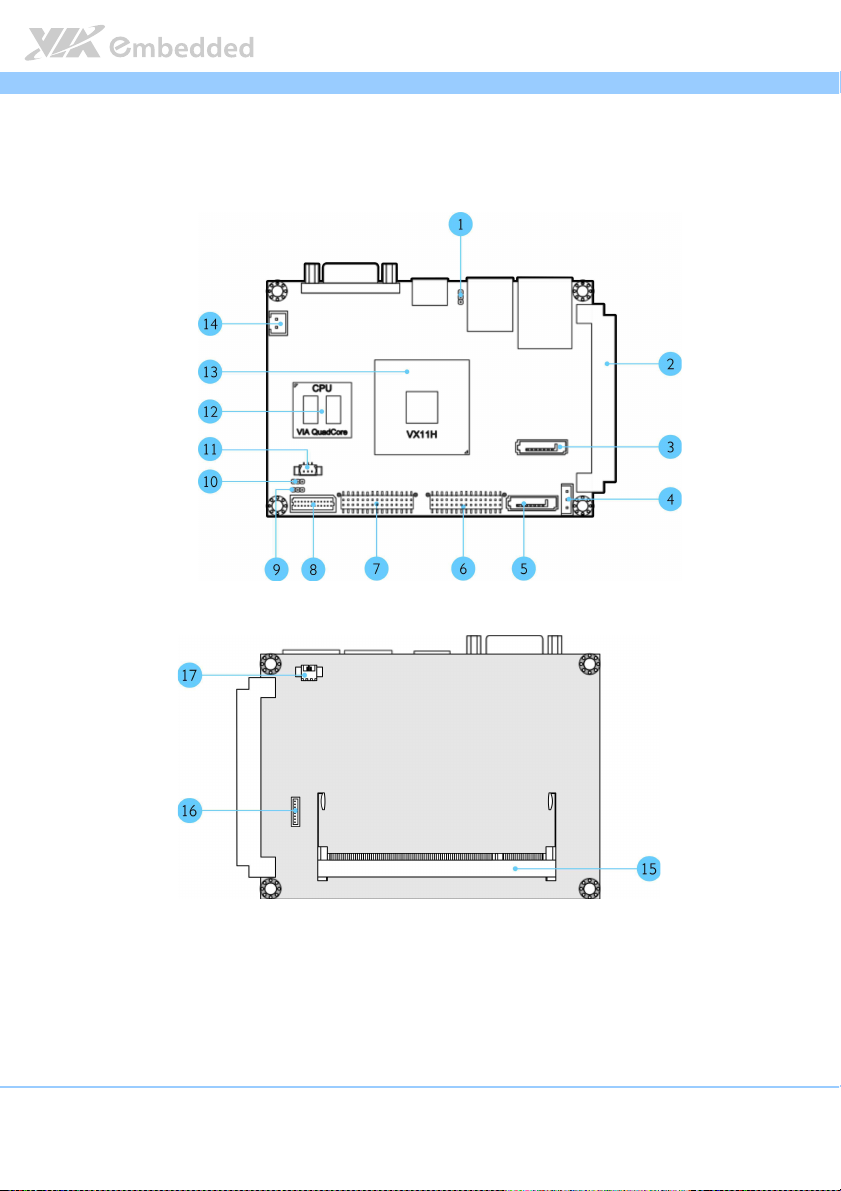
1.3. Layout Diagram
P910 User Manual
User Manual
P910P910
User ManualUser Manual
Figure
Figure 1111: Layout diagram of
: Layout diagram of the EPIA
Figure Figure
: Layout diagram of : Layout diagram of
the EPIA----P910 mainboard (top and bottom view)
the EPIAthe EPIA
P910 mainboard (top and bottom view)
P910 mainboard (top and bottom view)P910 mainboard (top and bottom view)
7
Page 19

EPIA
EPIA----P910
EPIAEPIA
Item
Item Description
ItemItem
1 JM1: Clear CMOS jumper
2 CN3: High Speed Extension Slot
3 SATA connector 2
4 PWR2: SATA power connector
5 SATA connector 1
6 CN2: Audio+USB 2.0+Front Panel combination pin header
7 CN1: KB/MS/LPC/GPIO/SMBus combination pin header
8 LVDS1: LVDS connector
9 JM3: Panel power selector
10 JM2: Backlight power selector
11 FAN1: System/CPU fan
12 Eden® X4
13 VX11H chipset
14 PWR1: DC-in power connector
15 SODIMM1: DDR3 SODIMM slot
16 J1: SPI connector
17 BAT1: CMOS battery connector
Table
Table 1111: Layout diagram description table of the EPIA
: Layout diagram description table of the EPIA----P910 mainboard
Table Table
: Layout diagram description table of the EPIA: Layout diagram description table of the EPIA
Description
DescriptionDescription
P910 mainboard
P910 mainboardP910 mainboard
P910 User Manual
User Manual
P910P910
User ManualUser Manual
8
Page 20
EPIA
EPIA----P910
EPIAEPIA
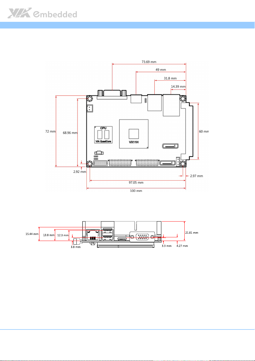
1.4. Product Dimensions
P910 User Manual
User Manual
P910P910
User ManualUser Manual
Figure
Figure 2222: Mounting holes and dimensions of the EPIA
: Mounting holes and dimensions of the EPIA----PPPP910
Figure Figure
: Mounting holes and dimensions of the EPIA: Mounting holes and dimensions of the EPIA
910
910910
9
Page 21
EPIA
EPIA----P910
P910 User Manual
EPIAEPIA
P910P910
1.5. Height Distribution
User Manual
User ManualUser Manual
Figure
Figure 3333: Height distribution of the EPIA
: Height distribution of the EPIA----P910 mainboard
Figure Figure
: Height distribution of the EPIA: Height distribution of the EPIA
P910 mainboard
P910 mainboardP910 mainboard
10
Page 22
EPIA
2.
2. I/O Interface
I/O Interface
2.2.
I/O InterfaceI/O Interface
The VIA EPIA-P910 has a wide selection of interfaces. It includes a selection of
frequently used ports as part of the external I/O coastline.
EPIA----P910
P910 User Manual
EPIAEPIA
P910P910
User Manual
User ManualUser Manual
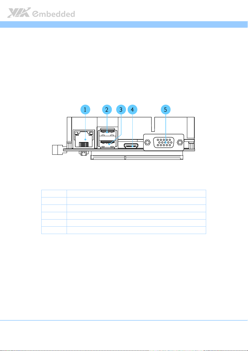
2.1. External I/O Ports
Figure
Figure 4444: External I/O ports
: External I/O ports
Figure Figure
: External I/O ports: External I/O ports
Item
Item Description
ItemItem
1 RJ1: Gigabit LAN port
2 USB1: USB 3.0 ports
3 USB2: USB 3.0 ports
4 HDMI1: Mini HDMI® port
5 VGA1: VGA port
Table
Table 2222: Layout diagram description table of external I/O ports
: Layout diagram description table of external I/O ports
Table Table
: Layout diagram description table of external I/O ports: Layout diagram description table of external I/O ports
Description
DescriptionDescription
11
Page 23
EPIA
EPIA----P910
P910 User Manual
EPIAEPIA
P910P910
User Manual
User ManualUser Manual
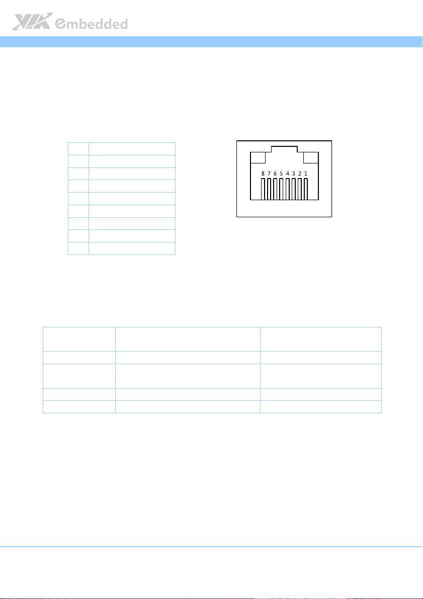
2.1.1. LAN port: Gigabit Ethernet
The integrated 8-pin Gigabit Ethernet port is using an 8 Position 8 Contact
(8P8C) receptacle connector (commonly referred to as RJ45). The Gigabit
Ethernet ports are controlled by VIA Fast Ethernet controller. The pinout of
the Gigabit Ethernet port is shown below.
Pin
Pin
Signal
Signal
PinPin
SignalSignal
1 Signal pair 1+
2 Signal pair 1-
3 Signal pair 2+
4 Signal pair 3+
5 Signal pair 3-
6 Signal pair 2-
7 Signal pair 4+
8 Signal pair 4-
Table
Table 3333: Gigabit Ethernet port pinout
: Gigabit Ethernet port pinout
Table Table
: Gigabit Ethernet port pinout: Gigabit Ethernet port pinout
Figure
Figure 5555: Gigabit Ethernet port pinout diagram
Figure Figure
The RJ-45 port has two individual LED indicators located on the front side to
show its Active/Link status and Speed status.
: Gigabit Ethernet port pinout diagram
: Gigabit Ethernet port pinout diagram: Gigabit Ethernet port pinout diagram
Link LED
(Left LED on RJ
(Left LED on RJ----45 connector)
(Left LED on RJ(Left LED on RJ
Link Off Off Off
Speed_10Mbit The LED is always On in either Green
Speed_100Mbit The LED is always On in Green color Flash in Yellow color
Speed_1000Mbit The LED is always On in Orange color
Table
Table 4444: Gigabit Ethernet LED color definition
: Gigabit Ethernet LED color definition
Table Table
: Gigabit Ethernet LED color definition: Gigabit Ethernet LED color definition
Link LED
Link LEDLink LED
45 connector)
45 connector)45 connector)
or Orange colors
Active LED
Active LED
Active LEDActive LED
(Right LED on RJ
(Right LED on RJ----45 connector)
(Right LED on RJ(Right LED on RJ
Flash in Yellow color
Flash in Yellow color
45 connector)
45 connector)45 connector)
12
Page 24
EPIA
EPIA----P910
P910 User Manual
EPIAEPIA
P910P910
User Manual
User ManualUser Manual
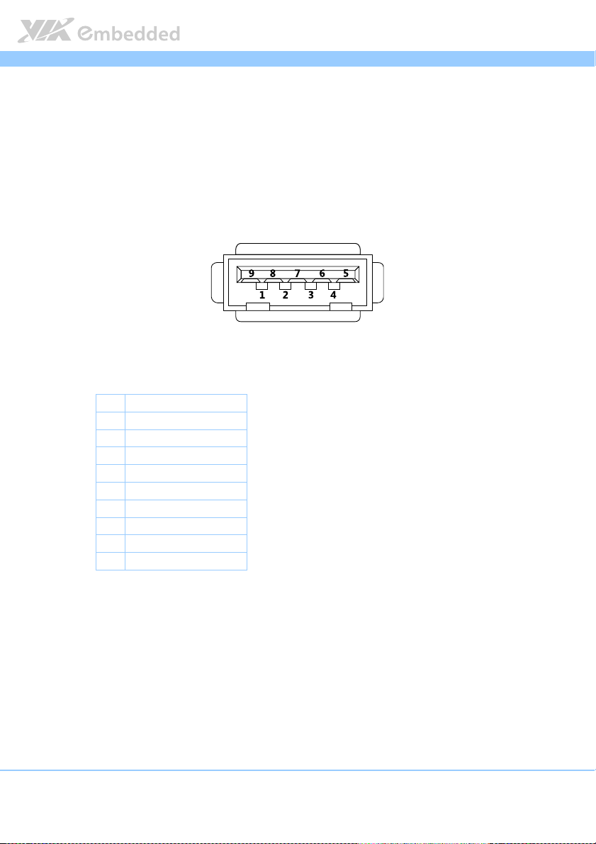
2.1.2. USB 3.0 Port
The EPIA-P910 mainboard provides two USB 3.0 ports, also known as
SuperSpeed USB. The USB 3.0 port has a maximum data transfer rate up to 5
Gbps and offers a backwards compatible with previous USB 2.0 specifications.
The USB 3.0 ports are using the USB Type-A receptacle connector. The pinout
of the typical USB 3.0 port is shown below.
Figure
Figure 6666: USB 3.0 port pinout diagram
: USB 3.0 port pinout diagram
Figure Figure
: USB 3.0 port pinout diagram: USB 3.0 port pinout diagram
Pin
Pin
Signal
Signal
PinPin
SignalSignal
1 +5V
2 Data-
3 Data+
4 GND
5 Rx-
6 Rx+
7 GND
8 Tx-
9 Tx+
Table
Table 5555: USB 3.0 port pinout
: USB 3.0 port pinout
Table Table
: USB 3.0 port pinout: USB 3.0 port pinout
13
Page 25
EPIA
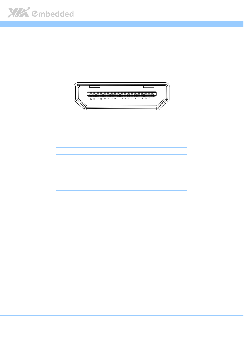
2.1.3. Mini HDMI
®
Port
EPIA----P910
P910 User Manual
EPIAEPIA
P910P910
User Manual
User ManualUser Manual
The integrated 19-pin HDMI® port uses an HDMI® Type C connector as
®
defined in the HDMI
®
HDMI
displays. The pinout of the Mini HDMI® port is shown below.
specification. The HDMI® port is for connecting to
Figure
Figure 7777: Mini HDMI
: Mini HDMI
Figure Figure
: Mini HDMI: Mini HDMI
®®®®
port pinout
port pinout diagram
port pinout port pinout
diagram
diagramdiagram
Pin
Pin
Signal
Table
Table 6666: HDMI
: HDMI
Table Table
: HDMI: HDMI
Signal Pin
PinPin
SignalSignal
1 TMDS Data2 Shield 2 TMDS Data2+
3 TMDS Data2– 4 TMDS Data1 Shield
5 TMDS Data1+ 6 TMDS Data1–
7 TMDS Data0 Shield 8 TMDS Data0+
9 TMDS Data0– 10 TMDS Clock Shield
11 TMDS Clock+ 12 TMDS Clock–
13 DDC/CEC Ground 14 CEC
15 SCL 16 SDA
17 Reserved (N.C. on
device)
19 Hot Plug Detect
®®®®
port pinout
port pinout
port pinout port pinout
Pin
Signal
Signal
PinPin
SignalSignal
18 +5V Power
14
Page 26
EPIA
EPIA----P910
P910 User Manual
EPIAEPIA
P910P910
User Manual
User ManualUser Manual
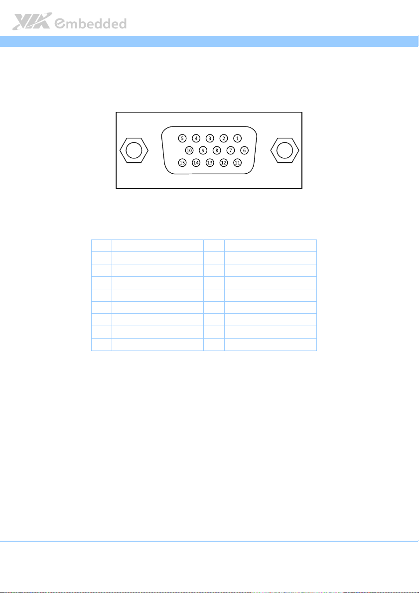
2.1.4. VGA Port
The 15-pin VGA port uses a female DE-15 connector. The VGA port is for
connecting to analog displays. The pinout of the VGA port is shown below.
Figure
Figure 8888: VGA port pinout diagram
: VGA port pinout diagram
Figure Figure
: VGA port pinout diagram: VGA port pinout diagram
Pin
Pin
Signal
Signal Pin
PinPin
SignalSignal
1 VGA-R 9 +5VCRT
2 VGA-G 10 Ground
3 VGA-B 11 NC
4 NC 12 VGA-SPD
5 Ground 13 VGA_HS
6 Ground 14 VGA_VS
7 Ground 15 VGA-SPCLK
8 Ground
Table
Table 7777: VGA port pinout
: VGA port pinout
Table Table
: VGA port pinout: VGA port pinout
Pin
PinPin
Signal
Signal
SignalSignal
15
Page 27
EPIA
EPIA----P910
P910 User Manual
EPIAEPIA
P910P910
User Manual
User ManualUser Manual
2.2. Onboard Connectors
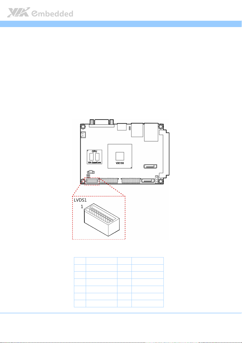
2.2.1. LVDS Connector
The mainboard has one 24-pin LVDS panel connector on the bottom side. The
onboard LVDS panel connector allows to connect the panel’s LVDS cable to
support the single-channel 18-bit/24-bit display. Backlight controls are
integrated into the LVDS panel connector pinout. The LVDS panel connector
is labeled as “LVDS1”. The pinout of the connector is shown below.
Figure
Figure 9999: LVDS connector
: LVDS connector
Figure Figure
: LVDS connector: LVDS connector
Pin
Pin
Si
Signal
gnal Pin
PinPin
SiSi
gnalgnal
1 LVDSD0- 2 LVDSD1-
3 LVDSD0+ 4 LVDSD1+
5 GND 6 GND
7 PVDD2 8 LVDSD2-
9 PVDD2 10 LVDSD2+
11 LCD1_DATA 12 GND
16
Pin Signal
Signal
PinPin
SignalSignal
Page 28

EPIA
13 LCD1_CLK 14 LVDSCLK+
15 GND 16 LVDSCLK-
17 VDD_BL 18 GND
19 VDD_BL 20 LVDSD3-
21 BLEN_1 22 LVDSD3+
23 BAK_ADJ 24 GND
Table
Table 8888: LVDS connector pinout
: LVDS connector pinout
Table Table
: LVDS connector pinout : LVDS connector pinout
Note:
Note:
Note:Note:
LVDS1 supports 18/24 bits EDID LCD, please ensure your LCD do support EDID. For any request of
None-EDID LCD, please contact sales for customized BIOS support
EPIA----P910
EPIAEPIA
P910 User Manual
User Manual
P910P910
User ManualUser Manual
17
Page 29

EPIA
EPIA----P910
P910 User Manual
EPIAEPIA
P910P910
User Manual
User ManualUser Manual
2.2.2. SATA Connectors
The two SATA connectors onboard can support up to 3 Gb/s transfer speeds.
1
Both SATA connectors have a 7th pin
Disk-on-Module (DOM). When a regular SATA hard drive is connected, the 7
pin will be a ground pin. The SATA connectors are labeled as “SATA1” and
“SATA2”. The pinout of the SATA connectors are shown below.
Figure
Figure 10
10: SATA connectors
Figure Figure
: SATA connectors
1010
: SATA connectors: SATA connectors
that can provide +5V power to a SATA
th
SATA1
SATA1 SATA2
SATA1SATA1
Pin
Pin
Signal
Signal Pin
PinPin
SignalSignal
1 GND 1 GND
2 STXP_0 2 STXP_1
3 STXN_0 3 STXN_1
4 GND 4 GND
5 SRXN_0 5 SRXN_1
6 SRXP_0 6 SRXP_1
7 GND/+5V
Table
Table 9999: SATA connector pinouts
: SATA connector pinouts
Table Table
: SATA connector pinouts: SATA connector pinouts
Note:
Note:
Note:Note:
The SATA connector pin 7 default setting is GND. The +5V supports is a factory option.
SATA2
SATA2SATA2
Pin Signal
Signal
PinPin
SignalSignal
7 GND/+5V
18
Page 30

EPIA
EPIA----P910
P910 User Manual
EPIAEPIA
P910P910
User Manual
User ManualUser Manual
2.2.3. SATA Power Connector
The onboard SATA power connector provides both +5V and +12V directly
through the mainboard to the SATA drives. The SATA power connector is
labeled as “PWR2”. The pinout of the SATA power connector is shown below.
Figure
Figure 11
11: SATA power connector
Figure Figure
: SATA power connector
1111
: SATA power connector: SATA power connector
Pin
Pin
Signal
Signal
PinPin
SignalSignal
1 +5V/1A
2 +12V/1A
3 GND
Table
Table 10
10: SATA power connector pinout
: SATA power connector pinout
Table Table
1010
: SATA power connector pinout: SATA power connector pinout
19
Page 31

EPIA
EPIA----P910
P910 User Manual
EPIAEPIA
P910P910
User Manual
User ManualUser Manual
2.2.4. KB/MS/LPC/GPIO/SMBus Combination Pin Header
The mainboard includes one KB, MS, LPC, GPIO and SMBus combination pin
header block labeled as “CN1”. The combination pin header is for connecting
KB, MS, LPC, General Purpose Input and Output and SMBus devices. The
pinout of the pin header is shown below.
Figure
Figure 12
12: KB/MS/LPC/GPIO/ SMBus combination pin header
Figure Figure
: KB/MS/LPC/GPIO/ SMBus combination pin header
1212
: KB/MS/LPC/GPIO/ SMBus combination pin header: KB/MS/LPC/GPIO/ SMBus combination pin header
Pin
Pin Signal
Signal Pin
PinPin
SignalSignal
1 LAD3 2 GND
3 LAD2 4 SIO_CLK1
5 LAD1 6 PCICLK3
7 -LFRAME 8 -LDRQ0
9 LAD0 10 SERIRQ
11 -PCIRST 12 GND
13 SMBDT_+3.3V 14 SMBCK_+3.3V
Pin Signal
Signal
PinPin
SignalSignal
20
Page 32

EPIA
15 +3.3V 16 +5V
17 -LID/GPI7 18 -INTB/GPIO8
19 -THRM/GPI9 20 -INTC/GPIO9
21 -EXTSMI/GPI5 22 GPIO12/GPIO12
23 -BATLOW/GPI4 24 GPIO32/GPIO32
25 GND 26 +5VSUS
27 KBDT 28 KBCK
29 MSDT 30 MSCK
Table
Table 11
11: KB/MS/LPC/GPIO/ SMBus combination pin header pinout
: KB/MS/LPC/GPIO/ SMBus combination pin header pinout
Table Table
1111
: KB/MS/LPC/GPIO/ SMBus combination pin header pinout: KB/MS/LPC/GPIO/ SMBus combination pin header pinout
EPIA----P910
EPIAEPIA
P910 User Manual
User Manual
P910P910
User ManualUser Manual
21
Page 33

EPIA
EPIA----P910
P910 User Manual
EPIAEPIA
P910P910
User Manual
User ManualUser Manual
2.2.5. Audio + USB 2.0 + Front Panel Combination Pin
Header
The mainboard includes one USB 2.0, Front Panel and Audio combination pin
header block labeled as “CN2”.The USB 2.0, front panel and audio
combination pin header is used to enable up to three USB 2.0 ports and to
connect the power switch, reset switch, power LED, suspend LED, HDD LED,
case speaker, SPDIF out, Line-Out, Line-In and MIC-In jacks. The pinout of the
pin header is shown below.
Figure
Figure 13
13: Audio + USB + Front panel combination pin header
Figure Figure
: Audio + USB + Front panel combination pin header
1313
: Audio + USB + Front panel combination pin header: Audio + USB + Front panel combination pin header
22
Page 34

EPIA
Pin
Pin
Signal
Signal Pin
PinPin
SignalSignal
1 GND 2 +5VSUSH1
3 USB_VD0- 4 USB_VD0+
5 USB_VD1- 6 USB_VD1+
7 USB_VD5- 8 USB_VD5+
9 GND 10 GND
11 +5V 12 +5VSUS
13 -HD_LED 14 -PWR_LED
15 PW_BN1- 16 GND
17 GND 18 SPEAK_BZ
19 RST_SW 20 GND
21 GND_AUD 22 LINER
23 MICIN_L 24 LINEL
25 MICIN_R 26 LINEOUT_R
27 SENSE_A 28 LINEOUT_L
29 SPDIF_TX0 30 GND
Table
Table 12
12: Audio + USB + Front panel combination pin header pinout
: Audio + USB + Front panel combination pin header pinout
Table Table
1212
: Audio + USB + Front panel combination pin header pinout: Audio + USB + Front panel combination pin header pinout
Pin
PinPin
Signal
Signal
SignalSignal
EPIA----P910
EPIAEPIA
P910 User Manual
User Manual
P910P910
User ManualUser Manual
23
Page 35

EPIA
EPIA----P910
P910 User Manual
EPIAEPIA
P910P910
User Manual
User ManualUser Manual
2.2.6. System/CPU Fan Connector
The System/CPU fan connector onboard runs on +12V and maintain
system/CPU cooling. The fan provides variable fan speeds controlled by the
BIOS. The System/CPU fan connector is labeled as “FAN1”. The pinout of the
system/fan connector is shown below.
Figure
Figure 14
14: System/CPU fan connector
Figure Figure
Table
Table 13
Table Table
: System/CPU fan connector
1414
: System/CPU fan connector: System/CPU fan connector
Pin
Pin
Signal
Signal
PinPin
SignalSignal
1 FANIN1
2 +12V FAN
3 GND
13: S
: System/CPU fan connector pinout
ystem/CPU fan connector pinout
1313
: S: S
ystem/CPU fan connector pinoutystem/CPU fan connector pinout
24
Page 36

EPIA
EPIA----P910
P910 User Manual
EPIAEPIA
P910P910
User Manual
User ManualUser Manual
2.2.7. DC-In Power Connector
The mainboard has an onboard DC-In 2-pin power connector to connect the
DC-In power cable. The DC-In power connector is labeled as “PWR1”. The
pinout of the DC-In power connector is shown below.
Fig
Figure
ure 15
15: DC
: DC----In power connector
FigFig
ure ure
In power connector
1515
: DC: DC
In power connectorIn power connector
Pin
Pin Signal
Signal
PinPin
SignalSignal
1 +12V
2 GND
Table
Table 14
14: DC
: DC----In power connector pinout
Table Table
In power connector pinout
1414
: DC: DC
In power connector pinoutIn power connector pinout
25
Page 37

EPIA
EPIA----P910
P910 User Manual
EPIAEPIA
P910P910
User Manual
User ManualUser Manual
2.2.8. CMOS Battery Connector
The mainboard is equipped with onboard CMOS battery connector used for
connecting the external cable battery that provides power to the CMOS RAM.
If disconnected all configurations in the CMOS RAM will be reset to factory
defaults. The CMOS battery connector is labeled as “BAT1”. The connector
pinout is shown below.
Figure
Figure 16
16: CMOS battery connector
Figure Figure
: CMOS battery connector
1616
: CMOS battery connector: CMOS battery connector
Pin
Pin
Signal
Signal
PinPin
SignalSignal
1 RTC_BAT
2 GND
Table
Table 15
15: CMOS battery connector pinout
: CMOS battery connector pinout
Table Table
1515
: CMOS battery connector pinout: CMOS battery connector pinout
26
Page 38

EPIA
EPIA----P910
P910 User Manual
EPIAEPIA
P910P910
User Manual
User ManualUser Manual
2.2.9. SPI Flash Connector
The mainboard has one 8-pin SPI flash connector. The SPI (Serial Peripheral
Interface) flash connector is used to connect to the SPI BIOS programming
fixture for updating the SPI flash ROM. The connector is labeled as “J1”. The
pinout of the connector is shown below.
Figure
Figure 17
17: SPI connector
Figure Figure
: SPI connector
1717
: SPI connector: SPI connector
Pin
Pin Signal
Signal
PinPin
SignalSignal
1 NC
2 NC
3 MSPIDO
4 MSPIDI
5 MSPICLK
6 MSPISSO
7 GND
8 SPIVCC
Table
Table 16
16: SPI connector pinout
: SPI connector pinout
Table Table
1616
: SPI connector pinout: SPI connector pinout
27
Page 39

EPIA
3.
3. Jumpers
Jumpers
3.3.
JumpersJumpers
EPIA----P910
P910 User Manual
EPIAEPIA
P910P910
User Manual
User ManualUser Manual
3.1. Clear CMOS Jumper
The onboard CMOS RAM stores system configuration data and has an onboard
battery power supply. To reset the CMOS settings, set the jumper on pins 2
and 3 while the system is off. Return the jumper to pins 1 and 2 afterwards.
Setting the jumper while the system is on will damage the mainboard. The
default setting is on pins 1 and 2.
Figure
Figure 18
18: CLEAR C
Figure Figure
Table
Table 17
Table Table
: CLEAR CMOS jumper
1818
: CLEAR C: CLEAR C
17: CLEAR CMOS jumper settings
: CLEAR CMOS jumper settings
1717
: CLEAR CMOS jumper settings: CLEAR CMOS jumper settings
MOS jumper
MOS jumperMOS jumper
Setting
Setting Pin 1
SettingSetting
Normal (default) On On Off
Clear CMOS Off On On
Pin 1 Pin 2
Pin 1Pin 1
Pin 2 Pin 3
Pin 2Pin 2
Pin 3
Pin 3Pin 3
28
Page 40

EPIA
EPIA----P910
EPIAEPIA
Note:
Note:
Note:Note:
Except when clearing the RTC RAM, never remove the cap from the CLEAR_CMOS jumper default
position. Removing the cap will cause system boot failure. Avoid clearing the CMOS while the system
is on; it will damage the mainboard.
P910 User Manual
User Manual
P910P910
User ManualUser Manual
29
Page 41

EPIA
EPIA----P910
P910 User Manual
EPIAEPIA
P910P910
User Manual
User ManualUser Manual
3.2. Backlight Power Select Jumper
The mainboard has a jumper that controls the input voltage delivered to the
LVDS inverter connector. The jumper is labeled as “JM2”. The jumper settings
are shown below.
Figure
Figure 19
19: Backlight power select jumper
Figure Figure
: Backlight power select jumper
1919
: Backlight power select jumper: Backlight power select jumper
Setting
Setting Pin1
SettingSetting
+12V (default)
+12V (default) On
+12V (default)+12V (default)
+5V
+5V Off
+5V+5V
Table
Table 18
18: Backlight po
: Backlight power select jumper settings
Table Table
1818
: Backlight po: Backlight po
wer select jumper settings
wer select jumper settingswer select jumper settings
30
Pin1 Pin2
Pin1Pin1
On On
OnOn
Off On
OffOff
Pin2
Pin2Pin2
On Off
OnOn
On On
OnOn
Pin3
Pin3
Pin3Pin3
Off
OffOff
On
OnOn
Page 42

EPIA
EPIA----P910
P910 User Manual
EPIAEPIA
P910P910
User Manual
User ManualUser Manual
3.3. Panel Power Control Jumper
The mainboard has one jumper that control the voltage delivered to the LVDS
panel connector. The jumper is labeled as “JM3”. The jumper settings are
shown below.
Figure
Figure 20
20:::: Panel Power Control jumper
Figure Figure
Table
Table 19
Table Table
31
Panel Power Control jumper
2020
Panel Power Control jumperPanel Power Control jumper
Setting
Setting Pin1
SettingSetting
+3.3V (default) Off On On
+5V On On Off
19: Panel Power Control jumper settings
: Panel Power Control jumper settings
1919
: Panel Power Control jumper settings: Panel Power Control jumper settings
Pin1
Pin1Pin1
Pin2
Pin2
Pin2Pin2
Pin3
Pin3
Pin3Pin3
Page 43

EPIA
4.
4. Expansion Slots
Expansion Slots
4.4.
Expansion SlotsExpansion Slots
EPIA----P910
P910 User Manual
EPIAEPIA
P910P910
User Manual
User ManualUser Manual
4.1. High Speed Extension Slot
The board-to-board slot labeled as “CN3” is a combination connector
reserved for connecting to a customized expansion card. The connector pinout
supports PCIe, LAN, USB 2.0, Audio, SDIO and SIM.
Figure
Figure 21
21: High Speed Extension Slot
Figure Figure
: High Speed Extension Slot
2121
: High Speed Extension Slot : High Speed Extension Slot
Pin
Pin Signal
PinPin
1 +5VSUS 2 +5VSUS
3 +5VSUS 4 +5VSUS
5 +5VSUS 6 +5VSUS
7 +12V 8 +12V
9 GND 10 GND
11 GND 12 GND
13 GND 14 GND
15 TVCLKRIN 16 MICIN2_R
17 SPDIF_TX1 18 MICIN2_L
19 MCVREF02 20 LINE2_R
21 SENSE_B 22 LINE2_L
23 GND 24 GND
Signal Pin
SignalSignal
Pin Signal
PinPin
Signal
SignalSignal
32
Page 44

EPIA
25 FANCTL2 26 SPEAK_BZ
27 FANIN2 28 GPIO37
29 -PCIRST 30 -RING
31 RST_SW 32 SD_CLK/MMC_CLK
33 PW_BN1- 34 CR_CMD
35 -SUSC 36 CR_D7
37 -SUSB 38 CR_D6
39 -CR_CD 40 CR_D5
41 -CR_WPD 42 CR_D4
43 VCCCR 44 CR_D3
45 CR_PWSELS 46 CR_D2
47 CR_PWSEL 48 CR_D1
49 CR_PWOFF 50 CR_D0
51 GND 52 GND
53 -HD_LED 54 VREFOUT_E
55 -PWR_LED 56 DVPCLKN
57 LVDSPWM1 58 DVPCLKP
59 DVPSPCLK 60 DVP1DE
61 DVPSPD 62 DVP1HS
63 SMBDT 64 DVP1VS
65 SMBCK 66 DVP1D11
67 -PEREQ1 68 DVP1D10
69 -PEXWAKE 70 DVP1D9
71 -PEX4RST 72 DVP1D8
73 -PEX2RST 74 DVP1D7
75 -PEX1RST 76 DVP1D6
77 GND 78 DVP1D5
79 USBHP3- 80 DVP1D4
81 USBHP3+ 82 DVP1D3
83 GND 84 DVP1D2
85 PEXRX2+ 86 DVP1D1
87 PEXRX2- 88 DVP1D0
89 GND 90 GND
91 PETN2 92 USBHP4-
93 PETP2 94 USBHP4+
95 GND 96 GND
97 PE6CLK- 98 USBHP2-
99 PE6CLK+ 100 USBHP2+
101 GND 102 GND
EPIA----P910
EPIAEPIA
P910 User Manual
User Manual
P910P910
User ManualUser Manual
33
Page 45

EPIA
103 PEXRX0- 104 PEXRX4-
105 PEXRX0+ 106 PEXRX4+
107 GND 108 GND
109 PETN0 110 PETN4
111 PETP0 112 PETP4
113 GND 114 GND
115 PE1CLK- 116 PE3CLK-
117 PE1CLK+ 118 PE3CLK+
119 GND 120 GND
Table
Table 20
20: High Speed E
: High Speed Extension Slot pinout
Table Table
2020
: High Speed E: High Speed E
xtension Slot pinout
xtension Slot pinoutxtension Slot pinout
EPIA----P910
EPIAEPIA
P910 User Manual
User Manual
P910P910
User ManualUser Manual
34
Page 46

EPIA
EPIA----P910
P910 User Manual
EPIAEPIA
P910P910
User Manual
User ManualUser Manual
4.2. DDR3 SODIMM Memory Slot
The mainboard provides one 204-pin DDR3 SODIMM slot that supports non-
ECC DDR3 1600/1333/1066 SODIMM memory modules. The memory slot can
accommodate up to 8 GB of DDR3 1600/1333/1066 memory. The memory slot
is labeled as “SODIMM1”. The location of the DDR3 memory slot is shown
below.
Figure
Figure 22
22: DDR3 SODIMM memory slot
Figure Figure
: DDR3 SODIMM memory slot
2222
: DDR3 SODIMM memory slot: DDR3 SODIMM memory slot
35
Page 47

EPIA
30
EPIA----P910
P910 User Manual
EPIAEPIA
P910P910
User Manual
User ManualUser Manual
4.2.1. Installing a Memory Module
Step 1
Step 1
Step 1Step 1
Align the notch on the SODIMM memory module with the protruding wedge
on the SODIMM memory slot. Insert the SODIMM memory module at a 30
degree angle relative to the SODIMM memory slot.
Figure
Figure 23
23: Inserting the memory module
Figure Figure
: Inserting the memory module
2323
: Inserting the memory module: Inserting the memory module
Step 2
Step 2
Step 2Step 2
Insert the SODIMM memory module between the two rows of pins. Then push
down until the locking clips lock the SODIMM memory module into place.
There will be a slight tension as the SODIMM memory module is being locked.
Figure
Figure 24
24: Locking the memory module
Figure Figure
36
: Locking the memory module
2424
: Locking the memory module: Locking the memory module
Page 48

EPIA
Step 3
Step 3
Step 3Step 3
EPIA----P910
P910 User Manual
EPIAEPIA
P910P910
User Manual
User ManualUser Manual
Install the memory thermal pad on the top of the DRAM memory module.
Figure
Figure 25
25: Installing memory thermal pad
Figure Figure
: Installing memory thermal pad
2525
: Installing memory thermal pad: Installing memory thermal pad
The memory thermal pad is used for transferring the heat dissipation of
memory to the thermal plate or bottom plate to attain memory cooling, and
to ensure the operating temperature of the memory module should not
exceed to 85°C. This helps to prevent damage of the memory module. The
memory thermal pad to be used is requires a certain thickness in order to
make contact with the memory thermal plate or bottom plate to excellently
disperse the heat.
Important:
Important:
Important:Important:
1. The customer/user should consider using the memory thermal pad and adding memory thermal
plate or bottom plate on their chassis design.
2. The memory thermal plate/bottom plate material to be used should have an excellent thermal
conductivity. Avoid using plastic or rubber materials.
3. The thickness of memory thermal pad should be based on customer’s design. However, the
minimum value of thermal conductivity K (W/m.k) is 1.5 and the maximum of hardness is 5
(Shore A).
37
Page 49

EPIA
EPIA----P910
P910 User Manual
EPIAEPIA
P910P910
User Manual
User ManualUser Manual
4.2.2. Removing a Memory Module
Step 1
Step 1
Step 1Step 1
To disengage the locking clips, push the locking clips horizontally outward
away from the SODIMM memory module.
Figure
Figure 26
26: Disengaging the SODIMM locking clips
Figure Figure
Step 2
Step 2
Step 2Step 2
: Disengaging the SODIMM locking clips
2626
: Disengaging the SODIMM locking clips: Disengaging the SODIMM locking clips
When the locking clips have cleared, the SODIMM memory module will
automatically pop up to the 30 degree angle. Remove the memory module.
Figure
Figure 27
27: Removing the memory module
Figure Figure
: Removing the memory module
2727
: Removing the memory module: Removing the memory module
38
Page 50

EPIA
5.
5. Hardware Installation
Hardware Installation
5.5.
Hardware InstallationHardware Installation
EPIA----P910
P910 User Manual
EPIAEPIA
P910P910
User Manual
User ManualUser Manual
5.1. Installing the P910-A Companion Card
(optional)
The optional P910-A companion card is connected through CN1 & CN2 pin
headers. Align and attach the board-to-board connector on the bottom of
P910-A with the CN1 and CN2 blocks on the EPIA-P910 mainboard.
Figure
Figure 28
28: Connecting P91
Figure Figure
: Connecting P910000----A companion card
2828
: Connecting P91: Connecting P91
Note:
Note:
Note:Note:
The P910-A companion card is for project based enquiries only. Please contact sales for detailed
information.
A companion card
A companion cardA companion card
39
Page 51

EPIA
EPIA----P910
P910 User Manual
EPIAEPIA
P910P910
User Manual
User ManualUser Manual
5.2. Installing into a Chassis
The EPIA-P910 can be fitted into any chassis that has the mounting holes
compatible with the standard Pico-ITX mounting hole locations. Additionally,
the chassis must meet the minimum height requirements for specified areas of
the mainboard.
5.2.1. Suggested minimum chassis dimensions
The figure below shows the suggested minimum space requirements that a
chassis should have in order to work well with the EPIA-P910.
Figure
Figure 29
29: Suggested minimum chassis dimensions
Figure Figure
: Suggested minimum chassis dimensions
2929
: Suggested minimum chassis dimensions: Suggested minimum chassis dimensions
Each side of the mainboard should have a buffer zone from the internal wall
of the chassis. The side of the mainboard that accommodates the I/O coastline
should have a buffer of 1.00 mm. The side on the opposite end of the I/O
coastline should have a buffer of at least 5.00 mm. The two sides adjacent to
the I/O coastline should have at least a 10.00 mm buffer.
40
Page 52

EPIA
EPIA----P910
P910 User Manual
EPIAEPIA
P910P910
User Manual
User ManualUser Manual
5.2.2. Suggested minimum chassis height
The figure below shows the suggested minimum height requirements for the
internal space of the chassis. It is not necessary for the internal ceiling to be
evenly flat. What is required is that the internal ceiling height must be strictly
observed for each section that is highlighted.
Figure
Figure 30
30: Suggested minimum internal chassis ceiling height
Figure Figure
: Suggested minimum internal chassis ceiling height
3030
: Suggested minimum internal chassis ceiling height: Suggested minimum internal chassis ceiling height
Note:
Note:
Note:Note:
In getting the minimum height requirements for internal space of the chassis, it is required to consider
the heights of the connectors (such as SPI connector, CMOS battery connector and DDR3 SODIMM
slot) on the bottom side of the EPIA-P910 mainboard.
41
Page 53

EPIA
EPIA----P910
P910 User Manual
EPIAEPIA
P910P910
User Manual
User ManualUser Manual
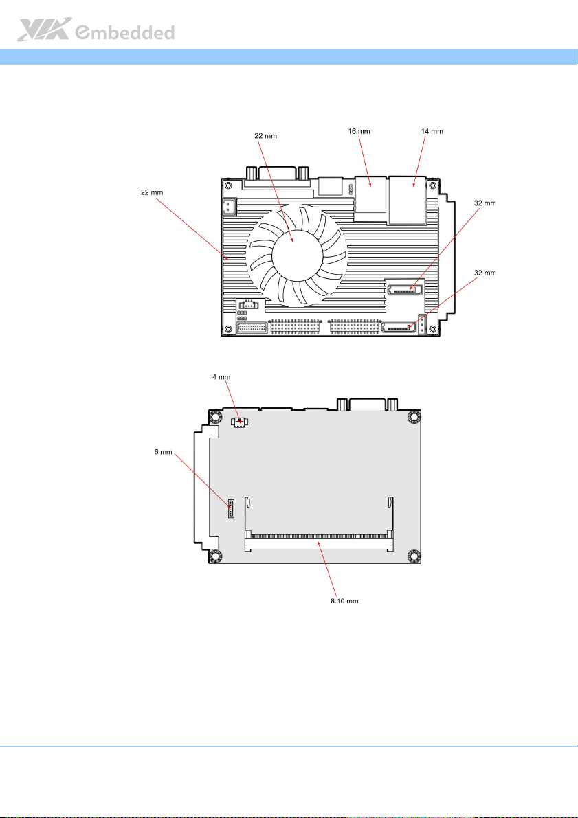
5.2.3. Suggested keepout areas
The figure below shows the areas of the mainboard that is highly suggested to
leave unobstructed.
Figure
Figure 31
31: Suggested keepout areas
Figure Figure
: Suggested keepout areas
3131
: Suggested keepout areas: Suggested keepout areas
42
Page 54

EPIA
6.
6. BIOS Setup Utility
BIOS Setup Utility
6.6.
BIOS Setup UtilityBIOS Setup Utility
EPIA----P910
EPIAEPIA
6.1. Entering the BIOS Setup Utility
P910 User Manual
User Manual
P910P910
User ManualUser Manual
Power on the computer and press Delete
sequence to enter the BIOS Setup Utility. If the entry point has passed, restart
the system and try again.
Delete during the beginning of the boot
DeleteDelete
6.2. Control Keys
Up
Up Move up one row
UpUp
Down
Down Move down one row
DownDown
Left
Left Move to the left in the navigation bar
LeftLeft
Right
Right Move to the right in the navigation bar
RightRight
Enter
Enter Access the highlighted item / Select the item
EnterEnter
Esc
Esc Jumps to the Exit screen or returns to the previous screen
EscEsc
1
Increase the numeric value
++++
1
----
Decrease the numeric value
2
F1
F1 General help
F1F1
F2
F2 Previous value
F2F2
F3
F3 Load optimized defaults
F3F3
F4
F4 Save all the changes and exit
F4F4
Note:
Note:
Note:Note:
1. Must be pressed using the 10-key pad.
2. The General help contents are only for the Status Page and Option Page setup menus.
43
Page 55

EPIA
EPIA----P910
EPIAEPIA
6.3. Getting Help
P910 User Manual
User Manual
P910P910
User ManualUser Manual
The BIOS Setup Utility provides a “General Help
accessed at any time by pressing F1
using and navigating the BIOS Setup Utility. Press Esc
General Help” screen. This screen can be
General HelpGeneral Help
F1. The help screen displays the keys for
F1F1
Esc to exit the help screen.
EscEsc
44
Page 56

EPIA
EPIA----P910
P910 User Manual
EPIAEPIA
P910P910
User Manual
User ManualUser Manual
6.4. System Overview
The System Overview screen is the default screen that is shown when the
BIOS Setup Utility is launched. This screen can be accessed by traversing the
navigation bar to the “Main” label.
Figure
Figure 32
32: Illustration of the Main menu screen
Figure Figure
: Illustration of the Main menu screen
3232
: Illustration of the Main menu screen: Illustration of the Main menu screen
6.4.1. BIOS Information
The content in this section of the screen shows the information about the
vendor, the Core version, UEFI specification version, the project version and
date & time of the project build.
6.4.2. Memory Information
This section shows the amount of memory that is installed on the hardware
platform.
6.4.3. System Language
This option allows the user to configure the language that the user wants to
use.
45
Page 57

EPIA
EPIA----P910
P910 User Manual
EPIAEPIA
P910P910
User Manual
User ManualUser Manual
6.4.4. System Date
This section shows the current system date. Press Tab
Shift+Tab
Shift+Tab to traverse left through the month, day, and year segments. The ++++
Shift+TabShift+Tab
and ---- keys on the number pad can be used to change the values. The weekday
name is automatically updated when the date is altered. The date format is
[Weekday, Month, Day, Year].
Tab to traverse right and
TabTab
6.4.5. System Time
This section shows the current system time. Press Tab
Shift+Tab
Shift+Tab to traverse left through the hour, minute, and second segments. The
Shift+TabShift+Tab
++++ and ---- keys on the number pad can be used to change the values. The time
format is [Hour : Minute : Second].
Tab to traverse right and
TabTab
46
Page 58

EPIA
EPIA----P910
P910 User Manual
EPIAEPIA
P910P910
User Manual
User ManualUser Manual
6.5. Advanced Settings
The Advanced Settings screen shows a list of categories that can provide
access to a sub-screen. Sub-screen links can be identified by the preceding
right-facing arrowhead.
Figure
Figure 33
33: Illustration of the Advanced Settings screen
Figure Figure
: Illustration of the Advanced Settings screen
3333
: Illustration of the Advanced Settings screen: Illustration of the Advanced Settings screen
The Advanced Settings screen contains the following links:
ACPI Settings
S5 RTC Wake Settings
CPU Configuration
SATA Configuration
F81801 H/W Monitor
Clock Generator Configuration
Onboard Configuration
47
Page 59

EPIA
EPIA----P910
P910 User Manual
EPIAEPIA
P910P910
User Manual
User ManualUser Manual
6.5.1. ACPI Settings
ACPI grants the operating system direct control over system power
management. The ACPI Configuration screen can be used to set a number of
power management related functions.
Figure
Figure 34
34: Illustration of the ACPI Settings screen
Figure Figure
: Illustration of the ACPI Settings screen
3434
: Illustration of the ACPI Settings screen: Illustration of the ACPI Settings screen
6.5.1.1.
6.5.1.1. Enable Hibernation
6.5.1.1.6.5.1.1.
Enable/disable system ability to Hibernate.
6.5.1.2.
6.5.1.2. ACPI Sleep State
6.5.1.2.6.5.1.2.
Select the highest ACPI sleep state the system will enter when the SUSPEND
button is selected. Available options are: Suspend Disabled / S1(CPU Stop
Clock) /S3 (Suspend to RAM) / Both S1 and S3 available for OS to choose.
Enable Hibernation
Enable HibernationEnable Hibernation
ACPI Sleep State
ACPI Sleep StateACPI Sleep State
48
Page 60

EPIA
EPIA----P910
P910 User Manual
EPIAEPIA
P910P910
User Manual
User ManualUser Manual
6.5.2. S5 RTC Wake Settings
Figure
Figure 35
35: Illustration of the
Figure Figure
6.5.2.1.
6.5.2.1. Wake system with Fixe
6.5.2.1.6.5.2.1.
Enable or disable system wake on alarm event. When enabled, system will
wake on the hr:min:sec specified.
: Illustration of the S5 RTC
3535
: Illustration of the : Illustration of the
Wake system with Fixed Time
Wake system with FixeWake system with Fixe
S5 RTC Wake Settings screen
Wake Settings screen
S5 RTC S5 RTC
Wake Settings screenWake Settings screen
d Time
d Timed Time
6.5.2.2.
6.5.2.2. Wake system with Dynamic Time
6.5.2.2.6.5.2.2.
Enable or disable Wake system with Dynamic Time.
Wake system with Dynamic Time
Wake system with Dynamic TimeWake system with Dynamic Time
49
Page 61

EPIA
EPIA----P910
P910 User Manual
EPIAEPIA
P910P910
User Manual
User ManualUser Manual
6.5.3. CPU Configuration
The CPU Configuration screen shows detailed information about the built-in
processor. In addition to the processor information, the thermal controls can
be set.
Figure
Figure 36
36: Illustration of
Figure Figure
: Illustration of CPU
3636
: Illustration of : Illustration of
CPU Configuration screen
Configuration screen
CPUCPU
Configuration screen Configuration screen
6.5.3.1.
6.5.3.1. TM3
6.5.3.1.6.5.3.1.
TM3
TM3TM3
The TM3 Function has two settings: Disabled and Enabled. When the setting is
changed to “Disabled”, the CPU’s built-in thermal sensor will not function.
When the setting is changed to “Enabled”, the thermal sensor will
automatically adjust the CPU ratio and V CORE to prevent the CPU from
overheating.
50
Page 62

EPIA
EPIA----P910
P910 User Manual
EPIAEPIA
P910P910
User Manual
User ManualUser Manual
6.5.4. SATA Configuration
The SATA Configuration screen allows the user to view and configure the
settings of the SATA configuration settings.
Figure
Figure 37
37: Illustration of SATA Configuration screen
Figure Figure
6.5.4.1.
6.5.4.1. SATA Mode
6.5.4.1.6.5.4.1.
: Illustration of SATA Configuration screen
3737
: Illustration of SATA Configuration screen: Illustration of SATA Configuration screen
SATA Mode
SATA ModeSATA Mode
This option allows the user to manually configure SATA controller for a
particular mode.
IDE Mode
IDE Mode
IDE ModeIDE Mode
Set this value to change the SATA to IDE mode.
AHCI Mode
AHCI Mode
AHCI ModeAHCI Mode
Set this value to change the SATA to AHCI mode.
51
Page 63

EPIA
EPIA----P910
P910 User Manual
EPIAEPIA
P910P910
User Manual
User ManualUser Manual
6.5.5. PC Health Status
The PC Health Status screen has no editable fields. The system temperature is
taken from an optional sensor that is connected to the J5 pin header.
Figure
Figure 38
38: Illustration of PC Health Status screen
Figure Figure
6.5.5.1.
6.5.5.1. Fan Turbo Mode
6.5.5.1.6.5.5.1.
This option allows the user to Enable or Disable Fan Turbo Mode.
: Illustration of PC Health Status screen
3838
: Illustration of PC Health Status screen: Illustration of PC Health Status screen
Fan Turbo Mode
Fan Turbo ModeFan Turbo Mode
52
Page 64

EPIA
EPIA----P910
P910 User Manual
EPIAEPIA
P910P910
User Manual
User ManualUser Manual
6.5.6. Clock Generator Configuration
The Clock Generator Configuration screen enables access to the Spread
Spectrum Setting feature.
Figure
Figure 39
39: Illustration of Clock Generator Configuration screen
Figure Figure
: Illustration of Clock Generator Configuration screen
3939
: Illustration of Clock Generator Configuration screen: Illustration of Clock Generator Configuration screen
6.5.6.1.
6.5.6.1. CPU Spread Spectrum
6.5.6.1.6.5.6.1.
The Spread Spectrum Setting feature enables the BIOS to modulate the clock
frequencies originating from the mainboard. The settings are in percentages of
modulation. Higher percentages result in greater modulation of clock
frequencies. This feature has 3 options: Disable, +-0.25% and -0.5%.
6.5.6.2.
6.5.6.2. PCIe Spread Spectrum
6.5.6.2.6.5.6.2.
Select PCIe Spread Spectrum. This feature has 2 options: Disable and -0.5%.
CPU Spread Spectrum
CPU Spread SpectrumCPU Spread Spectrum
PCIe Spread Spectrum
PCIe Spread SpectrumPCIe Spread Spectrum
53
Page 65

EPIA
EPIA----P910
P910 User Manual
EPIAEPIA
P910P910
User Manual
User ManualUser Manual
6.5.7. OnBoard Device Configuration
The OnBoard Device Configuration screen has the following features.
Figure
Figure 40
40: Illustration of
Figure Figure
6.5.7.1.
6.5.7.1. OnBoard LAN Enable
6.5.7.1.6.5.7.1.
The OnBoard LAN Enable feature determines whether the onboard LAN
controller will be used or not.
: Illustration of OnBoard Device Configuration screen
4040
: Illustration of : Illustration of
OnBoard LAN Enable
OnBoard LAN EnableOnBoard LAN Enable
OnBoard Device Configuration screen
OnBoard Device Configuration screenOnBoard Device Configuration screen
6.5.7.2.
6.5.7.2. EuP/ErP Lot6 support
6.5.7.2.6.5.7.2.
The EuP/ErP Lot6 Support feature enables the BIOS to reduce the power draw
to less than 1W when the system is in standby mode. This feature has two
options: enabled and disabled.
6.5.7.3.
6.5.7.3. S5 Wakeup On LAN
6.5.7.3.6.5.7.3.
The S5 Wakeup On LAN feature enables the BIOS to allow remote wake-up
from the S5 power off state through the PCI bus.
EuP/ErP Lot6 support
EuP/ErP Lot6 supportEuP/ErP Lot6 support
S5 Wakeup On LAN
S5 Wakeup On LANS5 Wakeup On LAN
54
Page 66

EPIA
6.5.7.4.
6.5.7.4. 1CH LVDS Backlight Co
6.5.7.4.6.5.7.4.
Backlight Control
Backlight Control
Backlight ControlBacklight Control
The Backlight Control feature control by VX11H enables the user to control
the brightness of the 1CH LVDS backlight. This feature has six options.
Level
Level
LevelLevel
0%, 20%, 40%, 60%, 80% and 100%.
6.5.7.5.
6.5.7.5. 2CH LVDS Backlight Control
6.5.7.5.6.5.7.5.
Backlight Control
Backlight Control
Backlight ControlBacklight Control
The Backlight Control feature control by VX11H enables the user to control
the brightness of the 2CH LVDS backlight. This feature has six options.
Level
Level
LevelLevel
0%, 20%, 40%, 60%, 80% and 100%.
1CH LVDS Backlight Control
1CH LVDS Backlight Co1CH LVDS Backlight Co
2CH LVDS Backlight Control
2CH LVDS Backlight Control2CH LVDS Backlight Control
ntrol
ntrolntrol
EPIA----P910
P910 User Manual
EPIAEPIA
P910P910
User Manual
User ManualUser Manual
55
Page 67

EPIA
EPIA----P910
P910 User Manual
EPIAEPIA
P910P910
User Manual
User ManualUser Manual
6.6. Chipset Settings
The Chipset Settings screen shows a list of categories that can provide access
to a sub-screen. Sub-screen links can be identified by the preceding right-
facing arrowhead.
Figure
Figure 41
41: Illustration of Chipset Settings screen
Figure Figure
: Illustration of Chipset Settings screen
4141
: Illustration of Chipset Settings screen: Illustration of Chipset Settings screen
The Chipset Settings screen contains the following links:
DRAM Configuration
Video Configuration
PMU-ACPI Configuration
SDIO_CR Configuration
Others Configuration
56
Page 68

EPIA
EPIA----P910
P910 User Manual
EPIAEPIA
P910P910
User Manual
User ManualUser Manual
6.6.1. DRAM Configuration
The DRAM Configuration screen has two features for controlling the system
DRAM. All other DRAM features are automated and cannot be accessed.
Figure
Figure 42
42: Illustration of DRAM Configuration screen
Figure Figure
6.6.1.1.
6.6.1.1. DRAM Clock
6.6.1.1.6.6.1.1.
The DRAM Clock option enables the user to determine how the BIOS handles
the memory clock frequency. The memory clock can either be dynamic or
static. This feature has eleven options.
: Illustration of DRAM Configuration screen
4242
: Illustration of DRAM Configuration screen: Illustration of DRAM Configuration screen
DRAM Clock
DRAM ClockDRAM Clock
By SPD
By SPD
By SPDBy SPD
By SPD option enables the BIOS to select a compatible clock frequency for
the installed memory.
400 MHz
400 MHz
400 MHz400 MHz
The 400 MHz option forces the BIOS to be fixed at 800 MHz for DDR3
memory modules.
533 MHz
533 MHz
533 MHz533 MHz
The 533 MHz option forces the BIOS to be fixed at 1066 MHz for DDR3
memory modules.
57
Page 69

EPIA
566 MHz
566 MHz
566 MHz566 MHz
The 566 MHz option forces the BIOS to be fixed at 1132 MHz for DDR3
memory modules.
600 MHz
600 MHz
600 MHz600 MHz
The 600 MHz option forces the BIOS to be fixed at 1200 MHz for DDR3
memory modules.
633 MHz
633 MHz
633 MHz633 MHz
The 633 MHz option forces the BIOS to be fixed at 1266 MHz for DDR3
memory modules.
667 MHz
667 MHz
667 MHz667 MHz
The 667 MHz option forces the BIOS to be fixed at 1334 MHz for DDR3
memory modules.
6.6.1.2.
6.6.1.2. VGA Share Memory (Frame Buffer)
6.6.1.2.6.6.1.2.
The VGA Share Memory feature enables the user to choose the amount of the
system memory to reserve for use by the integrated graphics controller. The
selections of memory amount that can be reserved are 256MB and 512MB.
VGA Share Memory (Frame Buffer)
VGA Share Memory (Frame Buffer)VGA Share Memory (Frame Buffer)
EPIA----P910
P910 User Manual
EPIAEPIA
P910P910
User Manual
User ManualUser Manual
58
Page 70

EPIA
EPIA----P910
P910 User Manual
EPIAEPIA
P910P910
User Manual
User ManualUser Manual
6.6.2. Video Configuration
The Video Configuration screen has features for controlling the integrated
graphics controller in the VX11H chipset.
Figure
Figure 43
43: Illustration of Video Configuration screen
Figure Figure
6.6.2.1.
6.6.2.1. Select Display Device Control
6.6.2.1.6.6.2.1.
Available selections are: Auto and Manual.
: Illustration of Video Configuration screen
4343
: Illustration of Video Configuration screen: Illustration of Video Configuration screen
Select Display Device Control
Select Display Device ControlSelect Display Device Control
6.6.2.2.
6.6.2.2. Select Display Device 1 and 2
6.6.2.2.6.6.2.2.
The Select Display Device feature enables the user to choose a specific
display interface. This feature has four options: CRT, LCD, LCD2 and HDMI. If
both Select Display Device 1 and Select Display Device 2 are set to the same
interface, then any display device connected to the other interface will not
function. For example, if both Select Display 1 and 2 are set to CRT, then no
data will be sent to the HDMI, LCD and LCD2 port.
6.6.2.3.
6.6.2.3. Panel Type
6.6.2.3.6.6.2.3.
The Panel Type feature enables the user to specify the resolution of the display
being used with the system. The panel types are predefined in the VGA VBIOS.
Select Display Device 1 and 2
Select Display Device 1 and 2Select Display Device 1 and 2
Panel Type
Panel TypePanel Type
59
Page 71

EPIA
EPIA----P910
P910 User Manual
EPIAEPIA
P910P910
User Manual
User ManualUser Manual
Panel Type
Panel Type
Panel TypePanel Type
00 640 x 480 08 800 x 480
01 800 x 600 09 1024 x 600
02 1024 x 768 10 1366 x 768
03 1280 x 768 11 1600 x 1200
04 1280 x 1024 12 1680 x 1050
05 1400 x 1050 13 1920 x 1200
06 1440 x 900 14 1920 x 1080
07 1280 x 800 15 1024 x 576
Resolution
Resolution Panel Type
ResolutionResolution
Panel Type
Panel TypePanel Type
Resolution
Resolution
ResolutionResolution
6.6.2.4.
6.6.2.4. Panel Type2
6.6.2.4.6.6.2.4.
Panel Type2
Panel Type2Panel Type2
The Panel Type feature enables the user to specify the resolution of display 2
being used with the system. The panel types are predefined in the VGA VBIOS.
Panel Type
Panel Type
Panel TypePanel Type
00 640 x 480 08 800 x 480
01 800 x 600 09 1024 x 600
02 1024 x 768 10 1366 x 768
03 1280 x 768 11 1600 x 1200
04 1280 x 1024 12 1680 x 1050
05 1400 x 1050 13 1920 x 1200
06 1440 x 900 14 1920 x 1080
07 1280 x 800 15 1024 x 576
Resolution
Resolution Panel Type
ResolutionResolution
Panel Type
Panel TypePanel Type
Resolution
Resolution
ResolutionResolution
60
Page 72

EPIA
EPIA----P910
P910 User Manual
EPIAEPIA
P910P910
User Manual
User ManualUser Manual
6.6.3. PMU_ACPI Configuration
The PMU_ACPI Configuration screen can be used to set a number of power
management related functions.
Figure
Figure 44
44: Illustration of PMU_ACP
Figure Figure
6.6.3.1.
6.6.3.1. Other Control
6.6.3.1.6.6.3.1.
: Illustration of PMU_ACPI Configuration screen
4444
: Illustration of PMU_ACP: Illustration of PMU_ACP
Other Control
Other ControlOther Control
I Configuration screen
I Configuration screenI Configuration screen
Figure
Figure 45
45: Illustration of Other Control screen
Figure Figure
: Illustration of Other Control screen
4545
: Illustration of Other Control screen: Illustration of Other Control screen
61
Page 73

EPIA
EPIA----P910
P910 User Manual
EPIAEPIA
P910P910
User Manual
User ManualUser Manual
6.6.3.1.1.
6.6.3.1.1. AC Loss Auto
6.6.3.1.1.6.6.3.1.1.
AC Loss Auto----restart
AC Loss AutoAC Loss Auto
restart
restartrestart
AC Loss Auto-restart defines how the system will respond after AC power has
been interrupted while the system is on. There are three options.
Power Off
Power Off
Power OffPower Off
The Power Off option keeps the system in an off state until the power button
is pressed again.
Power On
Power On
Power OnPower On
The Power On option restarts the system when the power has returned.
Last State
Last State
Last StateLast State
The Last State option restores the system to its previous state when the power
was interrupted.
6.6.3.1.2.
6.6.3.1.2. USB S4 WakeUp
6.6.3.1.2.6.6.3.1.2.
USB S4 WakeUp
USB S4 WakeUpUSB S4 WakeUp
The USB S4 WakeUp enables the system to resume through the USB device
port from S4 state. There are two options: “Enabled” or “Disabled”.
62
Page 74

EPIA
EPIA----P910
P910 User Manual
EPIAEPIA
P910P910
User Manual
User ManualUser Manual
6.6.4. SDIO_CR Configuration
The SDIO_CR Configuration screen can be used to set SDIO_CR configuration
parameters.
Figure
Figure 46
46: Illustration of SDIO_CR Configuration screen
Figure Figure
: Illustration of SDIO_CR Configuration screen
4646
: Illustration of SDIO_CR Configuration screen: Illustration of SDIO_CR Configuration screen
6.6.4.1.
6.6.4.1. SDIO Host Controller
6.6.4.1.6.6.4.1.
Available selections are: Enabled and Disabled.
6.6.4.2.
6.6.4.2. SDIO Specification Ver3.0 Suppo
6.6.4.2.6.6.4.2.
Available selections are: Enabled and Disabled.
6.6.4.3.
6.6.4.3. Voltage Support 1.8v
6.6.4.3.6.6.4.3.
Available selections are: Enabled and Disabled.
6.6.4.4.
6.6.4.4. High Speed Support
6.6.4.4.6.6.4.4.
Available selections are: Enabled and Disabled.
6.6.4.5.
6.6.4.5. Driver Type Select
6.6.4.5.6.6.4.5.
Available selections are: Type A, Type B, Type C and Type D.
SDIO Host Controller
SDIO Host ControllerSDIO Host Controller
SDIO Specification Ver3.0 Support
SDIO Specification Ver3.0 SuppoSDIO Specification Ver3.0 Suppo
Voltage Support 1.8v
Voltage Support 1.8vVoltage Support 1.8v
High Speed Support
High Speed SupportHigh Speed Support
Driver Type Select
Driver Type SelectDriver Type Select
rt
rtrt
63
Page 75

EPIA
6.6.4.6.
6.6.4.6. SDR50 Support
6.6.4.6.6.6.4.6.
Available selections are: Enabled and Disabled.
6.6.4.7.
6.6.4.7. SDR104 Support
6.6.4.7.6.6.4.7.
Available selections are: Enabled and Disabled.
6.6.4.8.
6.6.4.8. DDR50 Support
6.6.4.8.6.6.4.8.
Available selections are: Enabled and Disabled.
6.6.4.9.
6.6.4.9. SDR50 Tuning Enable
6.6.4.9.6.6.4.9.
Available selections are: Enabled and Disabled.
6.6.4.10.
6.6.4.10. Timer Count for Re
6.6.4.10.6.6.4.10.
Available selections are: 1 seconds, 2 seconds, 4 seconds, 8 seconds, 16
seconds, 32 seconds, 64 seconds, 120 seconds, 256 seconds, 512 seconds,
1024 seconds and get information from other source.
6.6.4.11.
6.6.4.11. Card Reader Host Cont
6.6.4.11.6.6.4.11.
Available selections are: Enabled and Disabled.
SDR50 Support
SDR50 SupportSDR50 Support
SDR104 Support
SDR104 SupportSDR104 Support
DDR50 Support
DDR50 SupportDDR50 Support
SDR50 Tuning Enable
SDR50 Tuning EnableSDR50 Tuning Enable
Timer Count for Re----Tuning
Timer Count for ReTimer Count for Re
Card Reader Host Controller 0
Card Reader Host ContCard Reader Host Cont
Tuning
TuningTuning
roller 0
roller 0roller 0
EPIA----P910
P910 User Manual
EPIAEPIA
P910P910
User Manual
User ManualUser Manual
64
Page 76

EPIA
EPIA----P910
P910 User Manual
EPIAEPIA
P910P910
6.6.5. Others Configuration
The Others Configuration screen can be used to set Watchdog Timer
Configuration and Keyboard/Mouse Wakeup Configuration.
Figure
Figure 47
47: Illustr
: Illustration of Others Configuration screen
Figure Figure
4747
ation of Others Configuration screen
: Illustr: Illustr
ation of Others Configuration screenation of Others Configuration screen
User Manual
User ManualUser Manual
6.6.5.1.
6.6.5.1. WATCHDOG Timer Enable
6.6.5.1.6.6.5.1.
When this feature is enabled, an embedded timing device automatically
prompts corrective action upon system malfunction detection.
6.6.5.2.
6.6.5.2. Keyboard/Mouse Wakeup Control
6.6.5.2.6.6.5.2.
When this feature is enabled, pressing any key of the keyboard or moving the
mouse can wake up the system from suspend.
WATCHDOG Timer Enable
WATCHDOG Timer EnableWATCHDOG Timer Enable
Keyboard/Mouse Wakeup Control
Keyboard/Mouse Wakeup ControlKeyboard/Mouse Wakeup Control
65
Page 77

EPIA
EPIA----P910
EPIAEPIA
6.7. Boot Settings
P910 User Manual
User Manual
P910P910
User ManualUser Manual
The Boot Settings screen has a single link that goes to the Boot Configuration
and Boot Option Priorities
Boot Option Priorities screens.
Boot Option PrioritiesBoot Option Priorities
Figure
Figure 48
48: Illustration of Boot Settings screen
Figure Figure
: Illustration of Boot Settings screen
4848
: Illustration of Boot Settings screen: Illustration of Boot Settings screen
Boot Configuration
Boot ConfigurationBoot Configuration
6.7.1. Boot Configuration
The Boot Settings Configuration screen has several features that can be run
during the system boot sequence.
6.7.1.1.
6.7.1.1. Quiet Boot
6.7.1.1.6.7.1.1.
Quiet Boot
Quiet BootQuiet Boot
The Quiet Boot feature hides all of the Power-on Self Test (POST) messages
during the boot sequence. Instead of the POST messages, the user will see an
OEM logo. This feature has two options: enabled and disabled.
66
Page 78

EPIA
EPIA----P910
EPIAEPIA
6.7.2. Boot Option Priorities
The Boot Option Priorities screen lists all bootable devices.
6.7.2.1.
6.7.2.1. Launch PXE OpROM policy
6.7.2.1.6.7.2.1.
Do not l
Do not launch
Do not lDo not l
Prevent the option for Legacy Network Device.
Legacy only
Legacy only
Legacy onlyLegacy only
Allow the option for Legacy Network Device.
Launch PXE OpROM policy
Launch PXE OpROM policyLaunch PXE OpROM policy
aunch
aunchaunch
P910 User Manual
User Manual
P910P910
User ManualUser Manual
67
Page 79

EPIA
EPIA----P910
P910 User Manual
EPIAEPIA
P910P910
User Manual
User ManualUser Manual
6.8. Save & Exit
The Save & Exit Configuration screen has the following features:
Figure
Figure 49
49: Illustration of Save & Exit sc
Figure Figure
: Illustration of Save & Exit screen
4949
: Illustration of Save & Exit sc: Illustration of Save & Exit sc
6.8.1. Save Changes and Exit
Save all changes to the BIOS and exit the BIOS Setup Utility. The “F10” hotkey
can also be used to trigger this command.
reen
reenreen
6.8.2. Discard Changes and Exit
Exit the BIOS Setup Utility without saving any changes. The “Esc” hotkey can
also be used to trigger this command.
6.8.3. Save Changes and Reset
Save all changes to the BIOS and reboot the system. The new system
configuration parameters will take effect.
68
Page 80

EPIA
EPIA----P910
P910 User Manual
EPIAEPIA
P910P910
User Manual
User ManualUser Manual
6.8.4. Discard Changes and Reset
This command reverts all changes to the settings that were in place when the
BIOS Setup Utility was launched. The “F7” hotkey can also be used to trigger
this command.
6.8.5. Save Options
Save Changes done so far to any of the setup options.
6.8.6. Save Changes
Save system configuration and continue. For some of the options it required to
reset the system to take effect.
6.8.7. Discard Changes
Undo the previous changes.
6.8.8. Restore Defaults
Restore default values for all setup options.
69
Page 81

EPIA
7.
7. Driver Installation
Driver Installation
7.7.
Driver InstallationDriver Installation
EPIA----P910
P910 User Manual
EPIAEPIA
P910P910
User Manual
User ManualUser Manual
7.1. Microsoft Driver Support
The VIA EPIA-P910 mainboard is compatible with Microsoft operating systems.
The latest Windows drivers can be downloaded from the VIA Embedded
website at www.viaembedded.com.
For embedded operating systems, the related drivers can be found in the VIA
Embedded website at www.viaembedded.com.
7.2. Linux Driver Support
The VIA EPIA-P910 mainboard is highly compatible with many Linux
distributions.
Support and drivers are provided through various methods including:
Drivers provided by VIA (binary only). An ARCM or NDA/BSLA may be
asked in order to get the drivers, please contact our sales representative
to submit a request.
Using a driver built into a distribution package
Installing a third party driver (such as the ALSA driver from the
Advanced Linux Sound Architecture project for integrated audio)
For OEM clients and system integrators developing a product for long term
production, other code and resources may also be made available. Contact
VIA Embedded to submit a request.
70
Page 82

EPIA
Appendix A.
Appendix A.
Appendix A.Appendix A.
Power Consumption Report
Power Consumption Report
Power Consumption ReportPower Consumption Report
Power consumption tests were performed on the VIA EPIA-P910. The
following tables represent the breakdown of the voltage, ampere and wattage
values while running common system applications.
EPIA----P910
P910 User Manual
EPIAEPIA
P910P910
User Manual
User ManualUser Manual
A.1. EPIA-P910-10Q
The tests were performed based on the following additional components:
CPU:
CPU: VIA Eden X4 U4650@1.0+ GHz
CPU:CPU:
Chipset:
Chipset: VX11H_A0
Chipset:Chipset:
Memo
Memory:
ry: Transcend TS512MSK64V3N-I/4GB
MemoMemo
ry:ry:
HDD SATA:
HDD SATA: Hitachi HTS545050B9A300 500GB +5V/700mA (#IST59)
HDD SATA:HDD SATA:
Power supply:
Power supply: FSP GROUP INC.
Power supply:Power supply:
MODEL NO. FSP060-DBAB1
AC Input: 100-240V~1.5A,50-60Hz
DC Output: 12.0V =5.0A MAX 60W
Operating System:
Operating System: Windows 7 + SP1 x64
Operating System:Operating System:
71
Page 83

EPIA
EPIA----P910
P910 User Manual
EPIAEPIA
P910P910
User Manual
User ManualUser Manual
A.1.1. Burn-in 3DMark06, 1280 x 1024 (Demo mode)
Quad Core 1.0+GHz [Enable PMON]
Test Condition
Test Condition Volts
Test ConditionTest Condition
Maximum 11.93 2.64 31.50
Average 11.93 1.75 20.88
Minimum 11.93 1.23 14.67
Volts Amperes
VoltsVolts
Amperes Watts
AmperesAmperes
Watts
WattsWatts
A.1.2. Burn-in 3DMark06, 1280 x 1024 (Demo mode)
Quad Core 1.0+GHz [Disable PMON]
Test Condition
Test Condition Volts
Test ConditionTest Condition
Maximum 12.03 1.96 23.58
Average 12.03 1.49 17.92
Minimum 12.03 1.10 13.23
Volts Amperes
VoltsVolts
Amperes Watts
AmperesAmperes
Watts
WattsWatts
A.1.3. PassMark Burn-in (CPU usage = 100%) Quad Core
1.0+GHz [Enable PMON]
Test Condition
Test Condition Volts
Test ConditionTest Condition
Maximum 11.69 3.14 36.71
Average 11.69 2.88 33.67
Minimum 11.69 2.62 30.63
Volts Amperes
VoltsVolts
Amperes Watts
AmperesAmperes
Watts
WattsWatts
A.1.4. PassMark Burn-in (CPU usage = 100%) Quad Core
1.0+GHz [Disable PMON]
Test Condition
Test Condition Volts
Test ConditionTest Condition
Maximum 11.87 2.47 29.32
Average 11.87 2.25 26.71
Minimum 11.87 2.01 23.86
72
Volts Amperes
VoltsVolts
Amperes Watts
AmperesAmperes
Watts
WattsWatts
Page 84

EPIA
EPIA----P910
P910 User Manual
EPIAEPIA
P910P910
User Manual
User ManualUser Manual
A.1.5. Power DVD 10.0 to Player H.264 1080P Movie
Quad Core 1.0+GHz [Enable PMON] Enable H/W
Acceleration
Test Condition
Test Condition Volts
Test ConditionTest Condition
Maximum 12.05 2.56 30.85
Average 12.05 1.38 16.23
Minimum 12.05 1.18 14.22
Volts Amperes
VoltsVolts
Amperes Watts
AmperesAmperes
Watts
WattsWatts
A.1.6. Power DVD 10.0 to Player H.264 1080P Movie
Quad Core 1.0+GHz [Disable PMON] Enable H/W
Acceleration
Test Condition
Test Condition Volts
Test ConditionTest Condition
Maximum 12.11 2.00 24.22
Average 12.11 1.20 14.53
Minimum 12.11 1.06 12.84
Volts Amperes
VoltsVolts
Amperes Watts
AmperesAmperes
Watts
WattsWatts
A.1.7. Power DVD 10.0 to Player MPEG2 1080P Movie
Quad Core 1.0+GHz [Enable PMON] Enable H/W
Acceleration
Test Co
Test Condition
ndition Volts
Test CoTest Co
nditionndition
Maximum 12.02 2.62 31.49
Average 12.02 1.60 19.23
Minimum 12.02 1.20 14.42
73
Volts Amperes
VoltsVolts
Amperes Watts
AmperesAmperes
Watts
WattsWatts
Page 85

EPIA
EPIA----P910
P910 User Manual
EPIAEPIA
P910P910
User Manual
User ManualUser Manual
A.1.8. Power DVD 10.0 to Player MPEG2 1080P Movie
Quad Core 1.0+GHz [Disable PMON] Enable H/W
Acceleration
Test Condition
Test Condition Volts
Test ConditionTest Condition
Maximum 12.06 2.17 26.17
Average 12.06 1.39 16.76
Minimum 12.06 1.06 12.78
Volts Amperes
VoltsVolts
Amperes Watts
AmperesAmperes
Watts
WattsWatts
A.1.9. Idle at Windows 7 x64 Quad Core 1.0+GHz
[Enable PMON]
Test Condition
Test Condition Volts
Test ConditionTest Condition
Maximum 12.09 1.40 16.93
Average 12.09 1.13 13.66
Minimum 12.09 1.06 12.82
Volts Amperes
VoltsVolts
Amperes Watts
AmperesAmperes
Watts
WattsWatts
A.1.10. Idle at Windows 7 x64 Quad Core 1.0+GHz
[Disable PMON]
Test Condition
Test Condition Volts
Test ConditionTest Condition
Maximum 12.16 1.56 18.97
Average 12.16 0.99 12.04
Minimum 12.16 0.91 11.07
74
Volts Amperes
VoltsVolts
Amperes Watts
AmperesAmperes
Watts
WattsWatts
Page 86

EPIA
EPIA----P910
P910 User Manual
EPIAEPIA
P910P910
User Manual
User ManualUser Manual
A.1.11. Suspend S1 Quad Core 1.0+GHz [Enable
PMON]
Test Condition
Test Condition Volts
Test ConditionTest Condition
Maximum 12.22 0.668 8.16
Average 12.22 0.661 8.08
Minimum 12.22 0.652 7.97
Volts Amperes
VoltsVolts
Amperes Watts
AmperesAmperes
Watts
WattsWatts
A.1.12. Suspend S1 Quad Core 1.0+GHz [Disable
PMON]
Test Condition
Test Condition Volts
Test ConditionTest Condition
Maximum 12.23 0.62 7.58
Average 12.23 0.61 7.46
Minimum 12.23 0.60 7.34
Volts Amperes
VoltsVolts
Amperes Watts
AmperesAmperes
Watts
WattsWatts
75
Page 87

EPIA
Appendix B.
Appendix B. Pin Header and
Appendix B.Appendix B.
Connector Vendor Lists
Connector Vendor Lists
Connector Vendor ListsConnector Vendor Lists
The following tables listed the pin headers and connectors vendor lists of
EPIA-P910 mainboard.
Pin Header and
Pin Header and Pin Header and
EPIA----P910
P910 User Manual
EPIAEPIA
P910P910
User Manual
User ManualUser Manual
B.1. EPIA-P910 Mainboard
Label
Label Function
LabelLabel
CN3 High Speed Extension Slot 120 SAMTEC ERF8-060-01-L-D-EM2-TR
CN1 KB/MS/LPC/GPIO/SMBus
CN2 Audio+USB 2.0+Front Panel
LVDS1 LVDS connector 24 ACES 87216-2416-06
JM2 Backlight power selector 3 Neltron 2199SA-03G-301523
JM3 Panel power selector 3 Neltron 2199SA-03G-301523
J1 SPI connector 8 Neltron 1600S-08-SM-TR
JM1 Clear CMOS jumper 3 Neltron 2199SA-03G-301523
BAT1 CMOS battery connector 2 Neltron 1251R-02-SM1-TR-F5
PWR2 SATA power connector 3 Neltron 2317SEH-03
PWR1 DC-in power connector 2 Neltron 2317SJ-02-F4
FAN1 System/CPU fan 3 Neltron 1251S-03-SM1-TR-F5
Table
Table 21
21: EPIA
: EPIA----P910 pin header and connector vendor lists
Table Table
2121
: EPIA: EPIA
Function Pins
FunctionFunction
combination pin header
combination pin header
P910 pin header and connector vendor lists
P910 pin header and connector vendor listsP910 pin header and connector vendor lists
Pins
PinsPins
30 PINREX 232-97-15GBEB
30 PINREX 232-97-15GBEB
Vendor
Vendor Part No.
VendorVendor
Part No.
Part No.Part No.
76
Page 88

 Loading...