

Page 1

user manual
EPIA-P830
Pico-ITX Embedded Board
1.13-03212018
-
181200
Page 2

II
Tested To Comply
With FCC Standards
FOR HOME OR OFFICE USE
Copyright
Copyright © 2010-2016 VIA Technologies Incorporated. All rights reserved.
No part of this document may be reproduced, transmitted, transcribed, stored in a
retrieval system, or translated into any language, in any form or by any means, electronic,
mechanical, magnetic, optical, chemical, manual or otherwise without the prior written
permission of VIA Technologies, Incorporated.
Trademarks
All trademarks are the property of their respective holders.
Disclaimer
No license is granted, implied or otherwise, under any patent or patent rights of VIA
Technologies. VIA Technologies makes no warranties, implied or otherwise, in regard to
this document and to the products described in this document. The information provided
in this document is believed to be accurate and reliable as of the publication date of this
document. However, VIA Technologies assumes no responsibility for the use or misuse of
the information (including use or connection of extra device/equipment/add-on card) in
this document and for any patent infringements that may arise from the use of this
document. The information and product specifications within this document are subject to
change at any time, without notice and without obligation to notify any person of such
change.
VIA Technologies, Inc. reserves the right the make changes to the products described in
this manual at any time without prior notice.
Regulatory Compliance
FCC-A Radio Frequency Interference Statement
This equipment has been tested and found to comply with the limits for a class A digital
device, pursuant to part 15 of the FCC rules. These limits are designed to provide
reasonable protection against harmful interference when the equipment is operated in a
commercial environment. This equipment generates, uses, and can radiate radio
frequency energy and, if not installed and used in accordance with the instruction manual,
may cause harmful interference to radio communications. Operation of this equipment in a
residential area is likely to cause harmful interference, in which case the user will be
required to correct the interference at his personal expense.
Notice 1
The changes or modifications not expressly approved by the party responsible for
compliance could void the user's authority to operate the equipment.
Notice 2
Shielded interface cables and A.C. power cord, if any, must be used in order to comply
with the emission limits.
Notice 3
The product described in this document is designed for general use, VIA Technologies
assumes no responsibility for the conflicts or damages arising from incompatibility of the
product. Check compatibility issue with your local sales representatives before placing an
order.
Page 3

III
Battery Recycling and Disposal
Only use the appropriate battery specified
for this product.
Do not re-use, recharge, or reheat an old
battery.
Do not attempt to force open the battery.
Do not discard used batteries with regular
trash.
Discard used batteries according to local regulations.
Safety Precautions
Always read the safety instructions carefully.
Keep this User's Manual for future reference.
All cautions and warnings on the equipment should be noted.
Keep this equipment away from humidity.
Lay this equipment on a reliable flat surface before setting
it up.
Make sure the voltage of the power source and adjust
properly 110/220V before connecting the equipment to the
power inlet.
Place the power cord in such a way that people cannot
step on it.
Always unplug the power cord before inserting any add-on
card or module.
If any of the following situations arises, get the equipment
checked by authorized service personnel:
The power cord or plug is damaged.
Liquid has penetrated into the equipment.
The equipment has been exposed to moisture.
The equipment has not worked well or you cannot get
it work according to User's Manual.
The equipment has dropped and damaged.
The equipment has obvious sign of breakage.
Do not leave this equipment in an environment
unconditioned or in a storage temperature above 60°C
(140°F). The equipment may be damaged.
Do not leave this equipment in direct sunlight.
Never pour any liquid into the opening. Liquid can cause
damage or electrical shock.
Do not place anything over the power cord.
Do not cover the ventilation holes. The openings on the
enclosure protect the equipment from overheating.
Page 4

IV
Box Contents and Ordering Information
Model Number Description
EPIA-P830-12L Standard kit
1 x P830-A daughter card
1 x SATA cable
1 x SATA power cable
1 x DC-in cable
P830-B This companion card is for project based
enquiries only. MOQ is required. Please
contact sales for detailed information.
Page 5

V
T
ABLE OF
C
ONTENTS
1 Overview ................................................................................................................. 1
Key Components ................................................................................................. 2
VIA Nano™ NanoBGA2 CPU .................................................................. 2
VIA VX900H System Processor ................................................................ 2
Layout........................................................................................................................ 3
Layout (I/O panel)............................................................................................... 5
Specifications ......................................................................................................... 6
2 Onboard I/O ......................................................................................................... 8
External I/O ............................................................................................................ 9
VGA port ............................................................................................................ 9
HDMI® port ....................................................................................................... 9
Gigabit LAN port ............................................................................................ 9
USB ports ............................................................................................................ 9
Onboard connectors ....................................................................................... 10
LVDS panel connector .............................................................................. 10
VGA and USB combination pin header ........................................... 11
SATA connectors .......................................................................................... 12
SATA power connector ............................................................................ 12
PCIe and USB combination connector ............................................. 13
USB and USB Device combination pin header ............................ 14
LAN pin header ............................................................................................ 15
UART connectors ......................................................................................... 16
LPC, SMBus, and GPIO combination pin header ......................... 17
SPI connector ................................................................................................. 18
CMOS battery connector ......................................................................... 18
Front panel and PS/2 combination pin header ........................... 19
Front audio pin header ............................................................................. 19
System fan connector ................................................................................ 20
DC-in power connector............................................................................ 20
SODIMM DDR3 memory slot ................................................................. 21
3 Onboard Jumpers ............................................................................................ 23
Clear CMOS jumper .................................................................................... 24
LVDS jumper settings ................................................................................. 25
LCD Backlight Power selector ................................................................ 25
4 Hardware Installation ...................................................................................... 26
Installing the P830-A ........................................................................................ 27
Page 6

VI
Installing the P830-B ........................................................................................ 29
5 BIOS Setup ............................................................................................................ 30
Entering the BIOS Setup Menu .................................................................. 31
Control Keys ......................................................................................................... 31
Getting Help ........................................................................................................ 32
Main Menu ........................................................................................................... 33
AMIBIOS ............................................................................................................ 33
Processor .......................................................................................................... 33
System Memory ............................................................................................. 33
System Time .................................................................................................... 33
System Date .................................................................................................... 33
Advanced Settings ............................................................................................ 34
CPU Configuration ........................................................................................... 35
Nano CPU TM3 Control ............................................................................ 35
IDE Configuration ............................................................................................. 36
IDE Drives .............................................................................................................. 37
PIO Mode ......................................................................................................... 37
DMA Mode ..................................................................................................... 37
SuperIO Configuration ................................................................................... 38
Serial Port Address, IRQ, and Type ....................................................... 38
Hardware Health Configuration ............................................................... 39
Smart FAN 1 ................................................................................................... 39
ACPI Configuration ........................................................................................... 40
Suspend Mode .............................................................................................. 40
ACPI Version Features ............................................................................... 40
APM Configuration ........................................................................................... 41
Power Button Mode ................................................................................... 41
Restore on AC / Power Loss ................................................................... 41
Resume on LAN ............................................................................................ 41
Resume On PS/2 KBC ................................................................................ 42
Wake-Up Key .................................................................................................. 42
Wake-Up Password..................................................................................... 42
Resume on PS/2 Mouse............................................................................ 42
Resume on RTC Alarm ............................................................................... 42
RTC Alarm Date (Days) .............................................................................. 43
System Time .................................................................................................... 43
Event Log Configuration ............................................................................... 44
View Event Log ............................................................................................. 44
Mark all events as read .............................................................................. 44
Clear Event Log ............................................................................................. 44
Spread Spectrum Configuration ................................................................ 45
Spread Spectrum Configuration ........................................................... 45
USB Configuration ............................................................................................ 46
USB Device Mode Enable ........................................................................ 46
Page 7

VII
USB Endpoint0 Ctrl Clk .............................................................................. 46
USBD Interface Selection .......................................................................... 46
CRB Configuration ............................................................................................ 47
DRAM Clock .................................................................................................... 47
Select Display Device 1 and 2 ................................................................ 47
Panel Type ....................................................................................................... 48
VGA Share Memory (Frame Buffer) ................................................... 48
OnChip HDAC Device............................................................................... 48
WATCH-DOG ................................................................................................ 48
Unit-Select ........................................................................................................ 48
Time-Select ....................................................................................................... 49
Backlight Control .......................................................................................... 49
Backlight PWM Clock ................................................................................. 49
VT6130 LAN Control 1 .............................................................................. 49
LAN Option ROM......................................................................................... 49
Boot Settings ........................................................................................................ 50
Boot Settings Configuration ......................................................................... 51
Quick Boot ....................................................................................................... 51
Quiet Boot ....................................................................................................... 51
Bootup Num-Lock ....................................................................................... 51
Wait For ‘F1’ If Error .................................................................................... 51
Hit ‘DEL’ Message Display ........................................................................ 52
Boot Device Priority .......................................................................................... 53
Security Settings.................................................................................................. 54
Change Supervisor Password ................................................................ 54
User Access Level ......................................................................................... 54
Change User Password ............................................................................ 55
Clear User Password ................................................................................... 55
Password Check............................................................................................ 55
Exit Options .......................................................................................................... 56
Save Changes and Exit .............................................................................. 56
Discard Changes and Exit ........................................................................ 56
Discard Changes .......................................................................................... 56
Load Optimal Defaults ............................................................................... 56
6 Driver Installation ............................................................................................... 57
Microsoft Driver Support ................................................................................ 58
Linux Driver Support ........................................................................................ 58
A Appendix .............................................................................................................. 59
Pin Header and Connector Vendor Lists............................................... 60
Page 8

1
1
Overview
Page 9

2
The VIA EPIA-P830 Pico-ITX Mainboard is a compact native x86
mainboard optimized for multimedia applications. It provides
support for high fidelity audio with its onboard VIA VT1708S High
Definition Audio codec.
The EPIA-P830 is based on the VIA VX900H Unified Digital Media
IGP chipset featuring the VIA C-9 HD with 2D/3D graphics and
video accelerators for rich digital media performance.
KEY COMPONENTS
VIA Nano™ NanoBGA2 CPU
The VIA Nano™ is a 64-bit superscalar processor in x86 platform
using a 65 nanometer process technology. It delivers an energyefficient, powerful performance, with cool and quiet operation all
within an ultra compact NanoBGA2 package measuring 21mm x
21mm. Perfectly fit for embedded system applications such as
industrial PCs, test machines, measuring equipment, digital
signage, medical PCs, monitoring systems, gaming machines, invehicle entertainment, and etc. The VIA Nano™ also boasts of
immersive multimedia performance, connectivity and computing
applications.
VIA VX900H System Processor
The VIA VX900H media system processor is an all-in-one, highly
integrated digital media IGP chipset featuring the latest video,
graphics and connectivity performance in a single chip measuring
just 31x31mm.
Page 10

3
LAYOUT
Page 11

4
Item
Description
Page
1 FAN1: System fan
20
2 CN5: LPC, SMBus, and GPIO combination pin header
17
3 CN4: Front panel and PS2 combination pin header
19
4 CN2: USB, and USB Device combination pin header
14
5 CN1: Front audio pin header
19
6 PWR2: SATA power connector
12
7 J1: UART port 2
16
8 SATA1, SATA2: SATA 3Gb/s connectors
12
9 C
N6: PCIe and USB 2.0 combination connector
13
10 CN3: LAN pin header
15
11 JM1: Clear CMOS jumper
24
12 HDMI1: HDMI
®
port 9
13 VGA_U
SB1: VGA and USB combination pin header
11
14 VX900H system processor
2
15 JM2 LCD power selector
25
16 JM3: Backlight power selector
25
17 PWR1: DC
-
in power connector
20
18 VIA Nano™ CPU
2
19 J2: UART port 1
16
20 SODIMM1: DDR3 SODIMM socket
20
21 LVDS1: LVDS con
nector
10
22 BAT1: CMOS battery connector
18
23 J3: SPI connector
18
Page 12
5
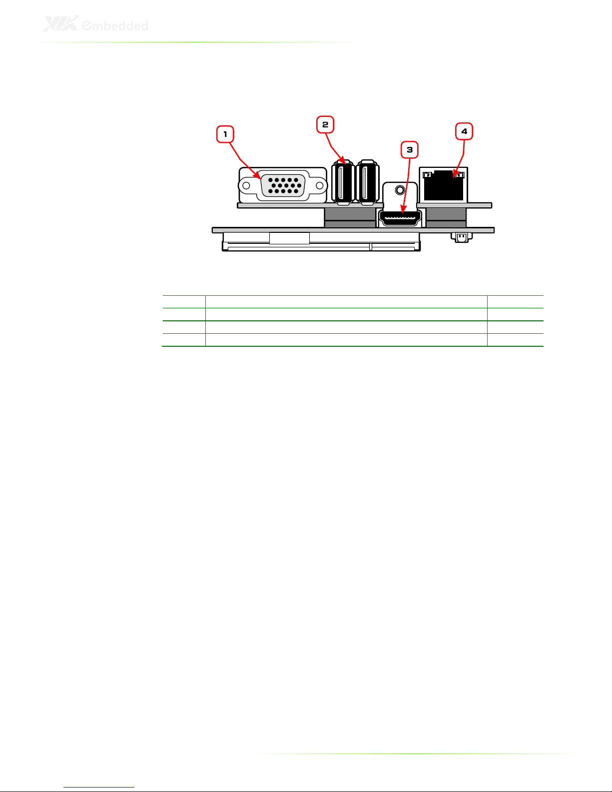
LAYOUT (I/O PANEL)
Item
Description
Page
1 VGA1: VGA port (on P830
-A) 9
2 USB1, USB2: USB 2.0 ports (on P830
-A) 9
3 HDMI1: HDMI
®
port 9
4 RJ1: Gigabit LAN port (on P830
-A) 9
Page 13

6
SPECIFICATIONS
Processor
VIA 1.2GHz U3300 Na
no processor
Chipset
VIA VX900H Unified Digital Media IGP Chipset
Super I/O
Fintek F81801U
-I
Memory
1 x DDR3 1066/800 MHz SODIMM slot
(supports a 4 GB module**)
VGA
Integrated VIA C
-9
HD 3D/2D graphics
Storage
2 x SATA 3Gb/s connectors
LAN
VIA
VT6130 PCIe Gigabit Ethernet controller
Audio
VIA VT1708S High Definition audio codec
I/O - 1 x Single
-
channel 24
-
bit LVDS connector
- 1 x LVDS inverter
- 1 x VGA-USB pin header
- 1 x 20-pin USB pin header for 5 additional USB ports
- 2 x 1-lane PCIe expansion connector (with one USB
support)
- 1 x LAN pin header
- 1 x Digital I/O pin header (GPI x 4, GPO x 4)
- 2 x UART pin headers
- 1 x LPC pin header
- 1 x SMBUS pin header
- 1 x Front audio pin header: Line-out, Line-in, Mic-in
- 1 x SPI pin header
- 1 x PS2 keyboard/mouse pin header
- 1 x Front-panel pin header
- 1 x System fan connector
- 1 x DC-in power connector (+12V±5%)
Back Panel I/O
-
1 x VGA port (on P830
-A)
- 1 x HDMI® port
- 1 x RJ-45 Gigabit LAN port (on P830-A)
- 2 x USB 2.0 ports (on P830-A)
BIOS
AMI BIOS
8Mbit SPI flash ROM
Operating System
Windows 7, Windows CE, Windows XPe, Windows
XP and Linux
Page 14

7
System Monitoring
-
Wake
-on-
LAN, Keyboard power
-
on, RTC Timer
power-on, Watch Dog Timer
- System power management, AC Power failure
recovery
Operating environment
0°C ~ 60°C
0% ~ 95% (relative humidity; non-condensing)
Form Factor
12 layer Pico
-
ITX (10 cm x 7.2 cm)
Compliance
CE/FCC/RoHS/BSMI
Note:
*Specifications are subject to change without notice
**The actual Max memory capacity that could be recognized under a 64-bit OS will
be less than 4GB due to the conflict in the memory space of the MMIO mapping.
*** As the operating temperature provided in the specifications is a result of the test
performed in VIA’s chamber, a number of variables can influence this result. Please
note that the working temperature may vary depending on the actual situation and
environment. It is highly suggested to execute a solid testing and take all the
variables into consideration when building the system. Please ensure that the system
runs well under the operating temperature in terms of application.
Page 15

8
2
Onboard I/O
Page 16
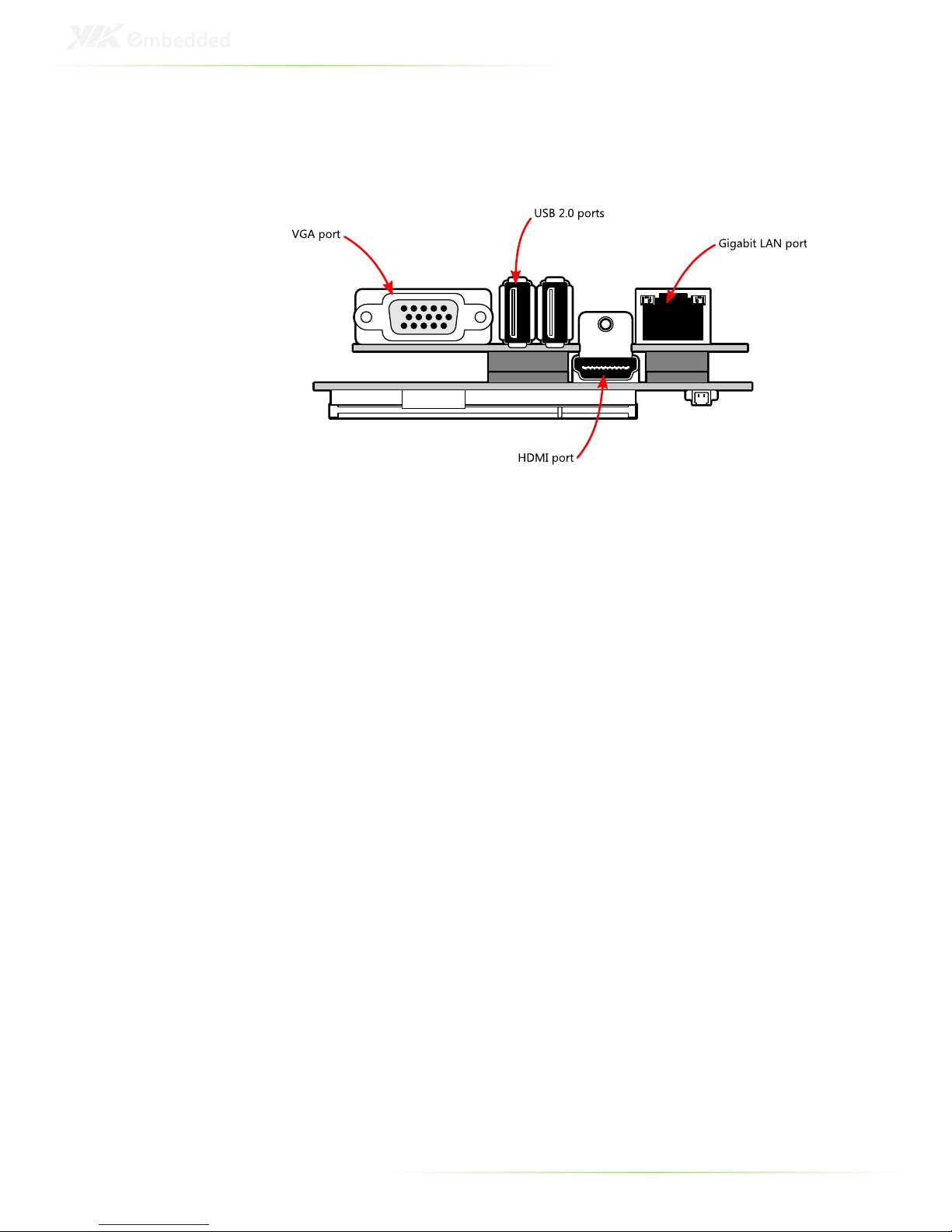
9
EXTERNAL I/O
The external I/O panel has the following ports:
VGA port
The 15-pin VGA port is for connecting to analog displays.
HDMI® port
The HDMI® port is for connecting to HDMI® displays.
Gigabit LAN port
The Gigabit Ethernet port is controlled through the VIA VT6130
PCIe Gigabit Ethernet controller.
USB ports
Two standard USB 2.0 ports are provided.
Page 17
10
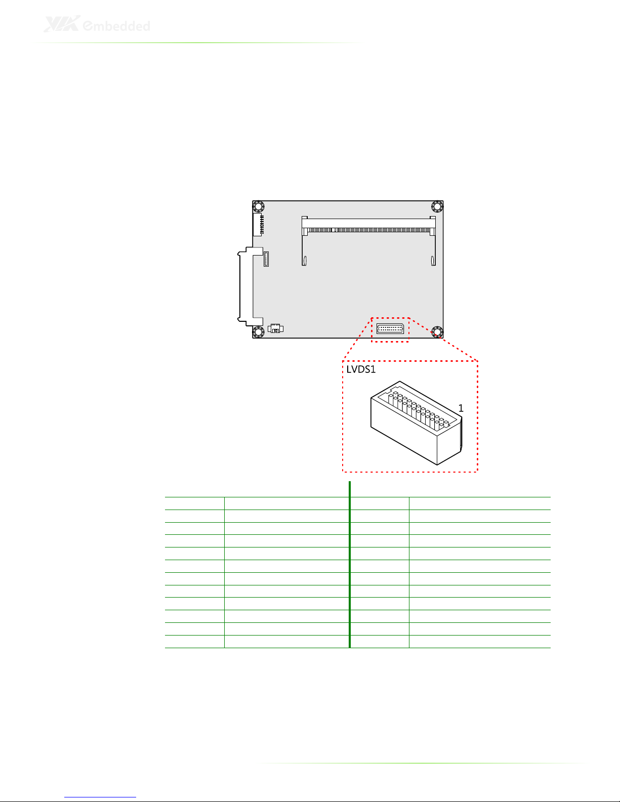
ONBOARD CONNECTORS
LVDS panel connector
The onboard LVDS panel connector (LVDS1) supports a singlechannel 24-bit display. Backlight controls are integrated into the
LVDS connector pinout.
Pin Signal
Pin Signal
1 LVDSD0
-- 2 LVDSD1
-
3 LVDSD0+
4
LVDSD1+
5 GND
6
GND
7 PVDD2
8
LVDSD2
-
9 PVDD2
10
LVDSD2+
11 LCD1_DATA
12
GND
13 LCD1_CLK
14
LVDSCLK+
15 GND
16
LVDSCLK
-
17 VDD_BL
18
GND
19 VDD_BL
20
LVDSD3
-
21 BLEN_1
22
LVDSD3+
23 BAK_ADJ
24
GND
Page 18
11
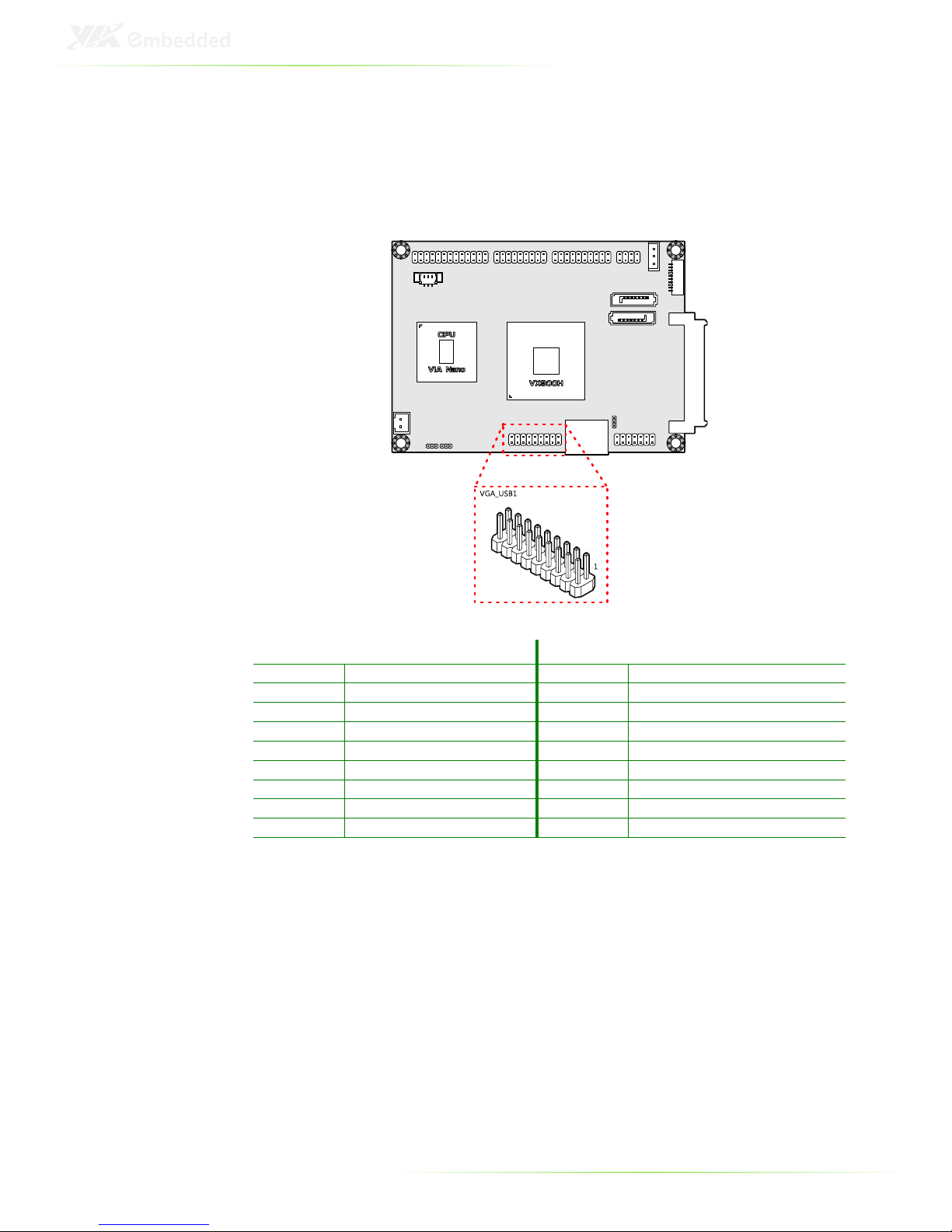
VGA and USB combination pin header
The VGA and USB combination pin header block (VGA_USB1) is
used to connect to the P830-A companion card. The pin header
block provides support for one VGA port and two USB 2.0 ports.
Pin Signal
Pin Signal
1 REDN
2
+5V
3 GREENN
4
GND
5 BLUEN
6
DDCDATAN
7 GND
8
DDCCLKN
9 VGP_IO
10 VS
11 HS 12 GND
13 +5VSUS
14
GND
15 USBHP5
- 16 USBHP4
-
17 USBHP5+
18
USBHP4+
Page 19
12
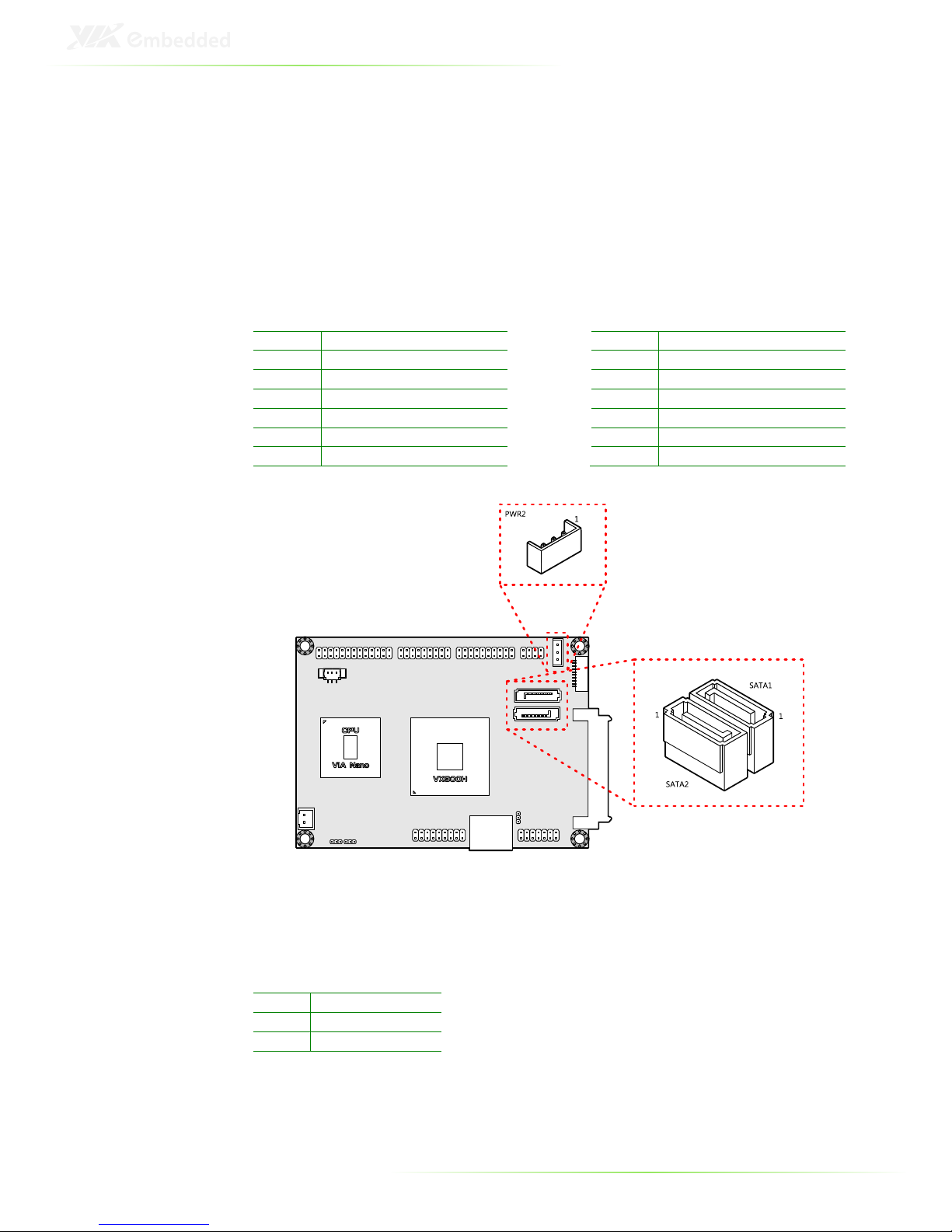
SATA connectors
There are two onboard SATA connectors that support data
transfer speeds up to 3 Gbps. Both SATA connectors have a 7th
pin that can provide +5V power to a SATA Disk-on-Module (DOM).
When a regular SATA hard drive is connected, the 7th pin will be a
ground pin.
SATA1
SATA2
Pin Signal
Pin Signal
1 GND
1 GND
2 STXP_0
2 STXP_1
3 STXN_0
3 STXN_1
4 GND
4 GND
5 SRXN_0
5 SRXN_1
6 SRXP_0
6 SRXP_1
7 +5V/GND
7 +5V/GND
SATA power connector
The onboard SATA power connector provides both +5V and
+12V directly through the mainboard to the SATA hard drives.
Pin Signal
1 +5V
2 +12V
3 GND
Page 20
13
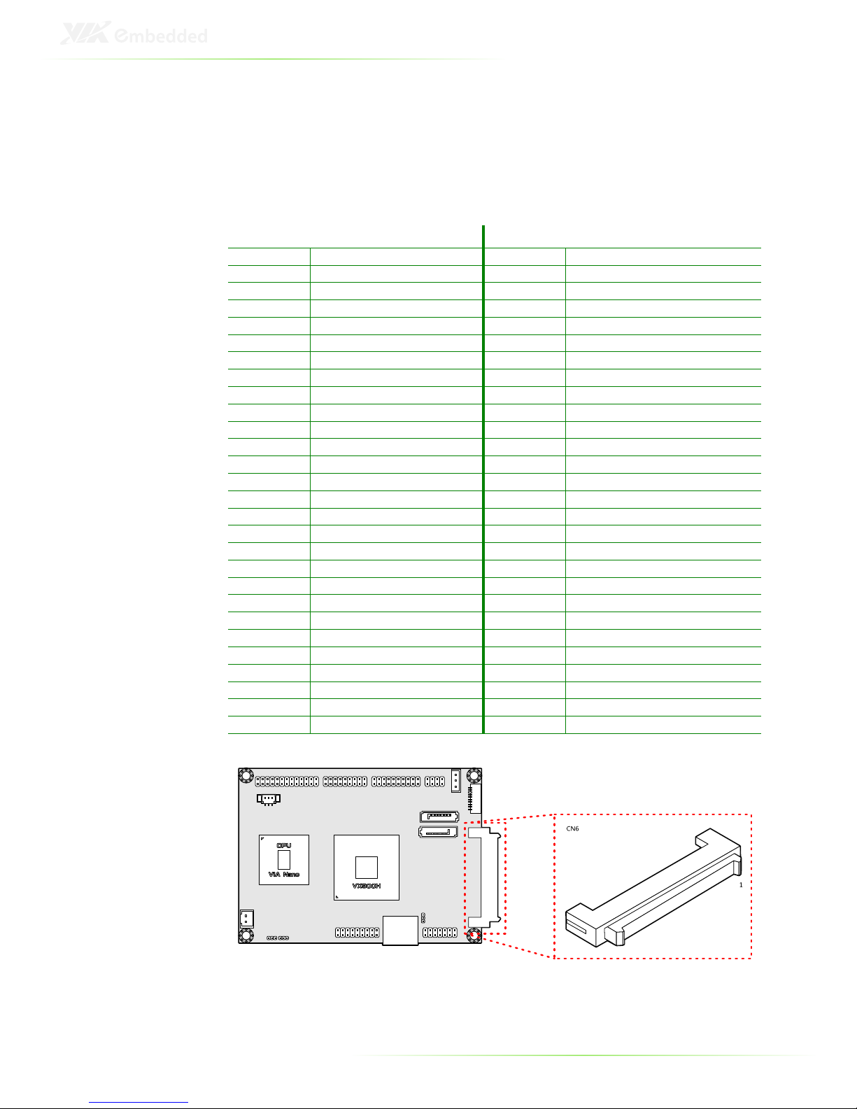
PCIe and USB combination connector
The onboard combination PCI Express and USB connector (CN6)
is for connecting directly to the P830-B companion card. Standard
PCIe or USB connectors are not supported. The connector pinout
supports the equivalent of two PCIe x1 ports and one USB 2.0 port.
Pin Signal
Pin Signal
1–25 Reserved
2–26 Reserved
27 GND
28
GND
29 +5V 30 -
LID
31 +5V 32 NC
33 +5V 34 GND
35 +3.3V
36
+12V
37 +3.3V
38
+5VSUS
39 GND
40
+5VSUS
41 SMBDT
42
+5VSUS
43 DMBCK
44 -PEX3RST
45 -
PEREQ1
46 -PEX2RST
47 -
PEXWAKE
48 -PEX1RST
49 GND
50
GND
51 PE3CLK
- 52 USBHP7
-
53 PE3CLK+
54
USBHP7+
55 GND
56
GND
57 PETN9
58
PEXRX9
-
59 PETP9
60
PEXRX9+
61 GND
62
GND
63 PETN8
64
PEXRX8
-
65 PETP8
66
PEXRX8+
67 GND
68
GND
69 NC 70 PE2CLK
-
71 NC 72 PE2CLK+
73 GND
74
GND
75 NC 76 NC
77 NC 78 NC
79 GND
80
GND
Page 21
14
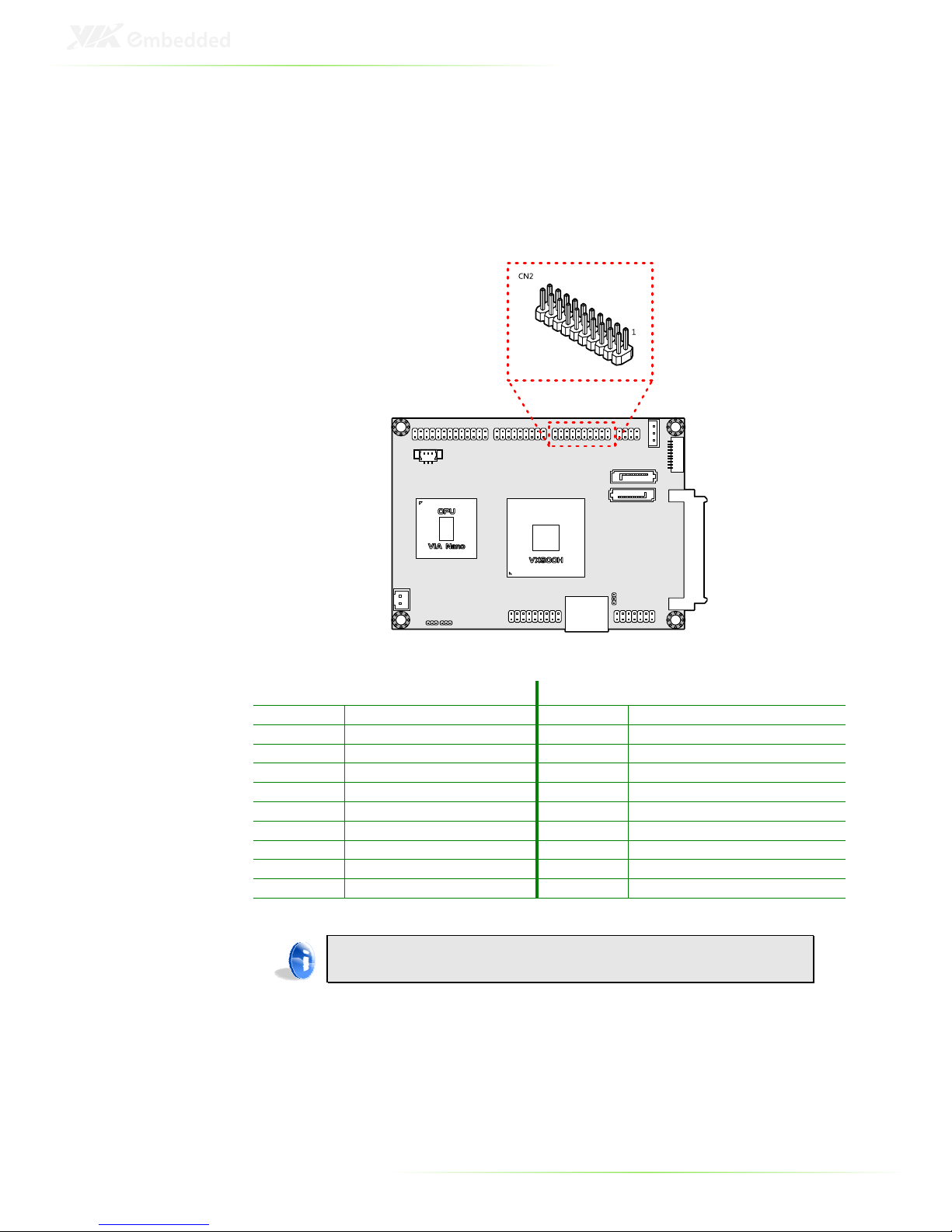
USB and USB Device combination pin
header
The onboard USB and USB Device combination pin header block
(CN2) enables the addition of five more USB 2.0 ports and one
USB device port.
Pin Signal
Pin Signal
1 GND
2
GND
3 GND
4
GND
5 USB_VD0+
6
USB_VD6+
7 USB_VD0
- 8 USB_VD6
-
9 +5VSUS
10
+5VSUS
11 USB_VD1
- 12 USB_VD3
-
13 USB_VD1+
14
USB_VD3+
15 +5VUSBD
16
+5VSUS
17 USBDP+
18
USB_VD2+
19 USBDP
- 20 USB_VD2
--
Note:
USB Device port is a reserved feature. Contact sales for specific support.
Page 22

15
LAN pin header
The onboard LAN pin header block (CN3) is used to connect to
the P830-A companion card. The pin header block provides
support for one RJ45 Gigabit Ethernet port.
Pin Signal
Pin Signal
1 VDDTXRX
2
AVDD33
3 TD2- 4
TD3-
5 TD2+
6
TD3+
7 TD0- 8
TD1-
9 TD0+ 10
TD1+
11 GMD
12
LED1
13 LED2
14
LNK_ACT
Page 23

16
UART connectors
The mainboard includes two UART ports. UART port 1 (J2) is the
12-pin port on the bottom side. UART port 2 (J1) is the 10-pin port
on the top side.
UART 2 (J1)
UART 1 (J2)
Pin Signal
Pin
Signal
1 +5V 1
GND
2 SIN2
2 -
LPCRST
3 SOUT2
3 SIO_GPIO16
4 -
DCD2
4 CTS1
5 -
RI2 5 -RTS1
6 GND
6 -
DSR1
7 -
DTR2
7 -DTR1
8 CTS2
8 SIN1
9 -
RTS2
9 SOUT1
10 -
DSR2
10 -
DCD1
11 -RI1
12
+3.3V
Page 24

17
LPC, SMBus, and GPIO combination pin
header
The mainboard includes one LPC, SMBus, and GPIO combination
pin header block (CN5).
Pin Signal
Pin Signal
1 GND
2
LAD3
3 SIO_CLK1
4
LAD2
5 PCICLK2
6
LAD1
7 -
LDRQ0
8 -LFRAME
9 SERIRQ
10
LAD0
11 NC 12 -
PCIRST
13 SMB_CLK
14
SMB_DAT
15 +5V 16 +
3.3V
17 -
INTD/GPIO12
18 -RING/GPI8
19 -
INTC/GPIO9
20 -THRM/GPI9
21 GPO12
22 -EXTSMI/GPI5
23 GPIO32
24 -BATLOW/GPI4
25 GND
26
GND
Page 25

18
SPI connector
The onboard SPI connector (J3) is for updating the SPI flash ROM.
Pin Signal
1 NC
2 NC
3 MSPIDO
4 MSP
IDI
5 MSPICLK
6 MSPISSO
7 GND
8 SPIVCC
CMOS battery connector
The onboard battery connector (BAT1) provides power to the
CMOS RAM. If disconnected all configurations in the CMOS RAM
will be reset to factory defaults.
Pin Signal
1 +VBAT
2 GND
Page 26

19
Front panel and PS/2 combination pin
header
The mainboard includes one Front Panel and PS/2 combination
pin header block (CN4). The PS/2 pin headers support one PS/2
keyboard and one PS/2 mouse.
Pin Signal
Pin Signal
1 +5VSUSLED1
2
+5VLED2
3 +5VSUSLED1
4 -HD_LED
5 GND
6
PW_BN
-
7 SPEAK_BZ
8
GND
9 GND
10
RST_SW
11 -
PWR_LED
12
GND
13 +5VSUS
14
GND
15 KBCK
16
KBDT
17 MSCK
18
MSDT
Front audio pin header
The mainboard has one pin header for connecting to front audio
Headphone-out and Mic-in jacks.
Pin Signal
Pin Signal
1 LINER
2
GND_AUD
3 LINEL
4
MICINL
5 LINEOUTR
6
MICINR
7 LINEOUTL
8
SENSE A
Page 27

20
System fan connector
The System fan (FAN1) runs on +5V and maintains system cooling.
Pin Signal
1 FANIN1
2 +5V FANCTL
3 GND
VIA Nano
CPU
VX900H
PWR1
1
FAN1
1
DC-in power connector
The mainboard has an onboard DC-In 2-pin power connector
(PWR1) to connect the DC-In power cable.
Pin Signal
1 DC-in (+12V±5%)
2 GND
Page 28

21
SODIMM DDR3 memory slot
The mainboard has one 204-pin DDR3 SODIMM slot that supports
non-ECC DDR3 1066/800 MHz memory modules. It can support
memory sizes up to 4 GB.
Page 29

22
Installing memory modules
Step 1
Locate the SODIMM slot in the mainboard and align the notch on
the SODIMM with the memory slot.
Step 2
Insert the SODIMM module at a 30 degree angle. Then push the
SODIMM down until it snaps into the locking mechanism.
Page 30

23
3
Onboard Jumpers
Page 31

24
Clear CMOS jumper
The onboard CMOS RAM stores system configuration data and
has an onboard battery power supply. To reset the CMOS settings,
set the jumper (JM1) on pins 2 and 3 while the system is off.
Return the jumper to pins 1 and 2 afterwards. Setting the jumper
while the system is on will damage the mainboard. The default
setting is on pins 1 and 2.
Setting
1 2 3
Normal Operation (default)
ON ON
OFF
Clear CMOS sett
ing OFF ON ON
Caution:
Except when clearing the RTC RAM, never remove the cap from the CLEAR_CMOS
jumper default position. Removing the cap will cause system boot failure. Avoid
clearing the CMOS while the system is on; it will damage the mainboard.
Page 32

25
LVDS jumper settings
The LVDS jumper (JM2) determines the input voltage for the LCD
connector.
1 2 3
+5V ON ON OFF
+3.3V (default)
OFF ON ON
LCD Backlight Power selector
The backlight jumper (JM3) determines the input voltage for the
LCD backlight inverter.
1 2 3
+12V (default)
ON ON
OFF
+5V
OFF ON ON
Page 33

26
4
Hardware
Installation
Page 34

27
INSTALLING THE P830-A
Step 1
Align the CON1 and CON2 connectors on the P830-A with the
VGA_USB1 combination pin header block and LAN pin header
block on the EPIA-P830, respectively. In the figure below, the
dotted rectangles represent the CON1 and CON2 connectors on
the bottom side of the P830-A companion card.
Page 35

28
Step 2
Then gently press down until the pins on the EPIA-P830
mainboard have been fully inserted into the CON1 and CON2
connectors of the P830-A companion card.
Step 3
Secure the EPIA-P830-A to the EPIA-P830 with two screws.
Page 36

29
INSTALLING THE P830-B
Step 1
Align the CN6 connector on the EPIA-P830 with the CN2
connector on the P830-B. Then gently insert the CN6 connector
into the CN2 connector until the CN6 connector is fully inserted.
Page 37

30
5
BIOS Setup
Page 38

31
ENTERING THE BIOS SETUP MENU
Power on the computer and press <
Delete
> during the beginning
of the boot sequence to enter the BIOS setup menu. If you missed
the BIOS setup entry point, restart the system and try again.
CONTROL KEYS
Keys
Description
Up Move to the previous item
Down
Move to the next item
Left Move to the previous tab
Right
Move to the next tab
Enter
Select the item
Esc Jumps to t
he Exit menu or returns to the main menu
from a submenu
+ (number pad)
Increase the numeric value
- (number pad)
Decrease the numeric value
F1 General help, only for Status Page Setup Menu and
Option Page Setup Menu
F7 Discard Changes
F9 Load Optimize
d defaults
F10 Save all the changes and exit
Page 39

32
GETTING HELP
The BIOS setup program provides a “
General Help
” screen. You
can display this screen from any menu/sub-menu by pressing
<F1>. The help screen displays the keys for using and navigating
the BIOS setup. Press <
Esc
> to exit the help screen.
Page 40

33
MAIN MENU
AMIBIOS
BIOS version number and related information.
Processor
This section describes the detected CPU name, speed, and
number of processors.
System Memory
This section describes the detected memory size.
System Time
Use the key “+” or “-” to configure system time. The time format is
[Hour : Minute : Second].
System Date
Use the key “+” or “-” to configure system Date. The date format is
[Day, Month, Date, Year].
Page 41

34
ADVANCED SETTINGS
Available submenus include the following:
• CPU Configuration
• IDE Configuration
• SuperIO Configuration
• Hardware Health Configuration
• ACPI Configuration
• APM Configuration
• Event Log Configuration
• Spread Spectrum Configuration
• USB Configuration
• CRB Configuration
Page 42

35
CPU CONFIGURATION
Nano CPU TM3 Control
This option is used to enable the internal thermal protection
features inside the onboard Nano CPU.
Settings
Description
Disabled
No thermal monitoring
Enabled
Enables Thermal Monitor 3
Page 43

36
IDE CONFIGURATION
Available submenus include the following:
• Primary IDE Master
• Primary IDE Slave
Page 44

37
IDE DRIVES
PIO Mode
The Programmed Input/Output mode is a data transfer method
that uses the CPU registers to transfer data.
Settings
Description
Auto
The Programmed Input/Output mo
de is automatically selected.
0 Maximum transfer rate of 3.3 MB/s. Cycle time: 600ns. Defined
in ATA specification.
1 Maximum transfer rate of 5.2 MB/s. Cycle time: 383ns. Defined
in ATA specification.
2 Maximum transfer rate of 8.3 MB/s. Cycle time: 24
0ns. Defined
in ATA specification.
3 Maximum transfer rate of 11.1 MB/s. Cycle time: 180ns. Defined
in ATA-2 specification.
4 Maximum transfer rate of 16.7 MB/s. Cycle time: 120ns. Defined
in ATA-2 specification.
DMA Mode
The Direct Memory Access mode is a data transfer method that
bypasses the CPU and directly transfers between the system
memory and the connected IDE device.
Settings
Description
Auto
The Direct Memory Access mode is automatically selected.
Page 45

38
SUPERIO CONFIGURATION
Serial Port Address, IRQ, and Type
The SuperIO configuration menu enables the BIOS to specifically
define the resources used for serial ports 1 and 2.
Port
Address/IRQ
1 3F8/IRQ4, 3E8/IRQ4, 2E8/IRQ3, Disabled
2 2F8/IRQ3, 3E8/IRQ4, 2E8/IRQ3, Disabled
Page 46

39
HARDWARE HEALTH CONFIGURATION
The Hardware Health Configuration displays all monitored
information.
Smart FAN 1
Settings
Description
Auto
Fan speed is dynamically adjusted as required to maintain
optimal system temperature.
Full Speed
Fan speed is fixed at the maximum RP
M of the system fan.
Page 47

40
ACPI CONFIGURATION
Suspend Mode
Select the ACPI state used for system suspend.
Settings
Description
S1(POS)
S1/Power On Suspend (POS) is a low power state. In this
state, no system context (CPU or chipset) is lost and
hardware maintains all system contexts
S3(STR)
S3/Suspend To RAM (STR) is a power
-
down state. In this
state, power is supplied only to essential components
such as main memory and wakeup-capable devices. The
system context is saved to main memory, and context is
restored from the memory when a "wakeup" event
occurs.
Auto
Depends on the OS to select the state.
ACPI Version Features
To enable RSDP pointers to 64-bit Fixed System Description Tables.
Settings
Description
ACPI v1.0
Supports ACPI v1.0
ACPI v2.0
Sup
ports ACPI v2.0
ACPI v3.0
Supports ACPI v3.0
Page 48

41
APM CONFIGURATION
Power Button Mode
Settings
Description
On/Off
Pressing the power button will Instantly cause the system to
power on or off.
Standby
Requires the user to press and hold the power button f
or 4
seconds before powering off the system.
Suspend
Pressing the power button will Instantly cause the system to
enter suspend mode.
Restore on AC / Power Loss
The field defines how the system will respond after an AC power
loss during system operation.
Settings
Description
Power Off
Keeps the system in an off state until the power button is
pressed.
Power On
Restarts the system when the power is back
Last State
Save in last state
Resume on LAN
Settings
Description
Enabled
The system will boot if an
y power management event is
triggered via LAN.
Disabled
The feature will be disabled.
Page 49

42
Resume On PS/2 KBC
Enables any detected keyboard activity to restore the system from
a power saving mode to an active state.
Settings
Description
S3 PS/2 keyboard acti
vity will be detected if the system is in
S3 power saving mode.
S3/S4/S5
PS/2 keyboard activity will be detected if the system is in
S3/S4/S5 power saving mode.
Disabled
Disables the detection of PS/2 keyboard activity.
Wake-Up Key
This option can only be modified when Resume on PS/2 KBC is
enabled.
Settings
Description
Any Key
Any key can be used to wake up the system.
Specific Key
This option unlocks the Wake
-
Up Password option.
Wake-Up Password
This option can only be modified when Wake-Up Key is set to
Specific Key. When selected, a prompt will be displayed requesting
a password for waking up the system. This password can consist
of up to 6 alphanumeric characters and some special characters.
Function keys and modifier keys (such as Ctrl, Alt, Del, etc.) cannot
be used.
Resume on PS/2 Mouse
Enable any PS/2 mouse activity to restore the system from the
power saving mode to an active state.
Settings
Description
S3 PS/2 mouse activity will be detected if the system is in S3
power saving mode.
S3/S4/S
5 PS/2 mouse activity will be detected if the system is in
S3/S4/S5 power saving mode.
Disabled
Disables the detection of PS/2 mouse activity.
Resume on RTC Alarm
This feature enables the BIOS to automatically power on at a
scheduled time.
Settings
Descr
iption
Enabled
Unlocks the RTC Alarm Date and System Time options.
Disabled
Support for this feature will be unavailable.
Page 50

43
RTC Alarm Date (Days)
This option enables the user to specify the frequency of the RTC
Alarm Date recurrence.
Settings
Description
Every Day
Triggers the RTC Alarm Date daily.
1 –
31 (days)
Triggers the RTC Alarm Date according to the increment
specified.
System Time
This option enables the user to specify the power on time for the
scheduled recurring date.
Page 51

44
EVENT LOG CONFIGURATION
View Event Log
This option enables users to view messages regarding recorded
events. Pressing the
<Enter>
button while this option is selected
will open a separate window containing a list of recorded event
logs.
Mark all events as read
This option enables users to quickly flag all event logs as having
been read — making it easier to distinguish old event logs from
future event logs.
Clear Event Log
This option enables users to completely empty the event log
history.
Page 52

45
SPREAD SPECTRUM CONFIGURATION
Spread Spectrum Configuration
The Spread Spectrum Configuration feature enables the BIOS to
help limit Electromagnetic Interference (EMI) emanating from the
system. Higher percentages reduce the EMI. However, higher
percentages may result in reduced system stability. If the system is
not placed near EMI sensitive electronics, it is recommended to
leave this feature disabled.
Settings
Description
0.1 –
0.9%
Increments of 0.1. Higher percentages have a greater
effect on reducing EMI.
Disabled
Support for thi
s feature will be unavailable.
Page 53

46
USB CONFIGURATION
The USB configuration page detects all connected USB devices.
USB Device Mode Enable
Settings
Description
Enabled
Unlocks the USB device port.
Disabled
Locks the USB device port.
Note:
The USB device port driver must be installed in order for the port to function.
USB Endpoint0 Ctrl Clk
This option is only available if
USB Device Mode Enable
is enabled.
Settings
Description
Enabled
Enable dynamic clock control
Disabled
Disable dynamic clock cont
rol
USBD Interface Selection
This option is only available if
USB Device Mode Enable
is enabled.
Settings
Description
Register Out
Select register out CCA interface
Original
Select original CCA interface
Page 54

47
CRB CONFIGURATION
DRAM Clock
Settings
Descr
iption
Auto
Auto adjusts the DRAM clock
400 MHz
Sets the DRAM clock to 400 MHz. DDR3 modules will
operate at 800 MHz.
533 MHz
Sets the DRAM clock to 533 MHz. DDR3 modules will
operate at 1066 MHz.
Select Display Device 1 and 2
The system can output data to two display devices simultaneously.
Settings
Description
CRT1
Specifies the CRT1 port as the display port being used.
LCD1
Specifies the LCD1 port as the display port being used.
HDMI
Specifies the HDMI
®
port as the display port being used.
EDP
Specifies the EDP port as the display port being used.
Page 55

48
Panel Type
This feature enables the user to specify the resolution of the display
being used with the system. The panel types are predefined in the
VGA VBIOS.
Settings
Description
00 640 x
480
01 800 x 600
02 1024 x 768
03 1280 x 768
04 1280 x 1024
05 1400 x 1050
06 1440 x 900
07 1280 x 800
08 800 x 480
09 1024 x 600
10 1366 x 768
11 1600 x 1200
12 1680 x 1050
13 1920 x 1200
14 1920 x 1080
15 1024 x 576
VGA Share Memory (Frame Buffer)
Settings
Description
64MB
Allocates 64 MB of system DRAM for the VGA frame buffer.
128MB
Allocates 128 MB of system DRAM for the VGA frame buffer.
256MB
Allocates 256 MB of system DRAM for the VGA frame buffer.
512MB
Allocates 512 MB of syst
em DRAM for the VGA frame buffer.
OnChip HDAC Device
Settings
Description
Enabled
Enables the HD audio codec in the VT1708S controller.
Disabled
Disables the HD audio codec in the VT1708S controller.
WATCH-DOG
Settings
Description
Enabled
Enables the
Watch
-
Dog timer.
Disabled
Disables the Watch
-
Dog timer.
Unit-Select
This option is only available if
WATCH-DOG
is enabled.
Settings
Description
Minutes
Sets the time increment in minutes
Seconds
Sets the time increment in seconds
Page 56

49
Time-Select
This option is only available if
WATCH-DOG
is enabled.
Settings
Description
0 Disable
1–255 Sets the number of units to count. If
Unit-Select
is set to
Minutes, the maximum acceptable integer is 17.
Backlight Control
This option sets the brightness control for an LCD device.
Settings
Description
Level 0
Sets the panel backlight brightness to 0%.
Level 1
Sets the panel backlight brightness to 25%.
Level 2
Sets the panel backlight brightness to 50%.
Level 3
Sets the panel backlight brightness to 75%.
Level 4
Sets the panel backlight brightness to 100%.
Backlight PWM Clock
This option is for selecting the clock frequency of the backlight
Pulse Width Modulation controls. The clock frequency depends on
the LVDS panel being used.
Settings
Description
14K Hz
Sets
the panel frequency to 14 kHz.
7K Hz
Sets the panel frequency to 7 kHz.
110 Hz
Sets the panel frequency to 110 Hz.
54.4 Hz
Sets the panel frequency to 54.4 Hz.
VT6130 LAN Control 1
Settings
Description
Enabled
Enable the onboard PCIe GigaLAN controlle
r.
Disabled
Disables the onboard PCIe GigaLAN controller and hides
it from the operating system.
LAN Option ROM
This option enables the PXE feature for booting via LAN.
Settings
Description
Enabled
Enables the PXE feature of the LAN controller.
Disabl
ed Does not load a separate ROM from the LAN controller.
Page 57

50
BOOT SETTINGS
The Boot Settings menu has the following submenus:
Boot Settings Configuration
Configuration settings during system boot.
Boot Device Priority
Page 58

51
BOOT SETTINGS CONFIGURATION
Quick Boot
Settings
Description
Enabled
Enables the BIOS to skip certain tests in order to reduce
boot up time.
Disabled
Support for this feature will be unavailable.
Quiet Boot
Settings
Description
Enabled
Displays an OEM logo instead of POST messages.
Disabled
Displays POST messages.
Bootup Num-Lock
Settings
Description
On For keyboards with a built
-
in 10
-
key pad, the BIOS will
force the keypad to behave in 10-key mode.
Off For keyboards with a built
-
in 10
-
key pad, the keypad will
behave as a cursor keypad.
Wait For ‘F1’ If Error
Settings
Description
Enabled
If an error is detected, the BIOS will pause booting and
wait for the user to press F1 to enter the BIOS setup
menu.
Disabled
Ignores errors while booting.
Page 59

52
Hit ‘DEL’ Message Display
Settings
Description
Enabled
Shows the POST message that informs the user how to
enter the BIOS setup menu. However, this message will
be hidden if the Display Logo option is enabled.
Disabled
Hides the POST message that informs the user how to
enter the BIOS setup menu.
Page 60

53
BOOT DEVICE PRIORITY
This menu automatically detects and lists all bootable storage
devices. The boot seek sequence can be changed in this menu.
Page 61

54
SECURITY SETTINGS
Change Supervisor Password
This option is for setting a password for accessing the BIOS setup
utility. When a password has been set, a password prompt will be
displayed whenever the BIOS setup utility is launched. This
prevents an unauthorized person from changing any part of the
system configuration.
When a supervisor password is set, the User Access Level and
Password Check options will be unlocked.
User Access Level
This feature controls the level of access a user (without the
supervisor password) is granted to the BIOS setup utility.
Settings
Description
No Access
Complete
ly locks the BIOS setup utility. The supervisor
password is required to access and change the BIOS
settings..
View Only
Only allows access to view the BIOS settings.
Limited
Only allows non
-
critical BIOS settings to be changed.
Changes are allowed to the following options:
System Time
System Date
Quick Boot
Display Logo
Full Access
Allows all BIOS settings to be changed except for the
Change Supervisor Password and User Access Level
options.
Page 62

55
Change User Password
This option is for setting a password for non-supervisors. When a
user password is set, the Clear User Password and Password
Check options will be unlocked.
Clear User Password
This option is only available when the user accesses the BIOS
Setup Utility when the user password has been specified.
Password Check
This feature is compulsory when the Change Supervisor Password
option is set. The user will have up to three chances to enter the
correct password before the BIOS forces the system to stop
booting. If the user does not enter the correct password, the
keyboard will also lock up. The only way to get past this is to do a
hard reboot (i.e., use the system reset button or cut off the power
to the system). A soft reboot (i.e., Ctrl+Alt+Del) will not work
because the keyboard will be locked.
Setti
ngs Description
Setup
Force users to enter a password in order to access the
BIOS setup utility.
Always
Force users to enter a password in order to boot up the
system.
Page 63

56
EXIT OPTIONS
Save Changes and Exit
Save all changes to the BIOS and exit the BIOS Setup Utility. The
“F10” hotkey can also be used to trigger this command.
Discard Changes and Exit
Exit the BIOS Setup Utility without saving any changes. The “Esc”
hotkey can also be used to trigger this command.
Discard Changes
This command reverts all changes to the settings that were in
place when the BIOS Setup Utility was launched. The “F7” hotkey
can also be used to trigger this command.
Load Optimal Defaults
Load optimal default values for all the setup items. The default
optimized values are defined by the mainboard manufacturer to
provide optimized environment for a basic system. The “F9” hotkey
can also be used to trigger this command.
Page 64

57
6
Driver Installation
Page 65

58
MICROSOFT DRIVER SUPPORT
The VIA EPIA-P830 mainboard is compatible with Microsoft
operating systems. The latest Windows drivers can be
downloaded from the VIA Embedded website at
http://www.viatech.com/en/boards/pico-itx/epia-p830/.
For embedded operating systems, the related drivers can be
found in the VIA Embedded website at www.viatech.com.
LINUX DRIVER SUPPORT
The VIA EPIA- P830 mainboard is highly compatible with many
Linux distributions.
Support and drivers are provided through various methods
including:
1. Drivers provided by VIA
2. Using a driver built into a distribution package
3. Visiting www.viatech.com for the latest updated drivers
4. Installing a third party driver (such as the ALSA driver from
the Advanced Linux Sound Architecture project for
integrated audio)
For OEM clients and system integrators developing a product for
long term production, other code and resources may also be
made available. Contact VIA Embedded to submit a request.
Page 66

59
A
Appendix
Page 67

60
PIN HEADER AND CONNECTOR
VENDOR LISTS
Label
Functio
n Pins
Vendor
Part No.
LVDS1
LVDS
24
ACES
87216
-
2416-06
SODIMM1
Memory
204 Foxconn
AS0A626
-
J6RG
-7H
SATA1, SATA2
SATA connector
7
Win Win
WATM
-
07DBN4A2B8UW
FAN1
Fan connector
3
Neltron
1251S
-03-
SM1-TR-F5
BAT1
Cable battery
connector
2 Neltron
1251R
-02-
SM1-TR-F5
VGA_USB1
VGA and USB
combination
connector
18 Neltron
2208SM
-
18G-BK-CP
PWR1
DC-
in connector
2
Neltron
2317SJ
-02-F4
PWR2
SATA power
connector
3 Neltron
2317SEH
-03
J1 UART port 2
connector
10 Neltron
1600R
-10-SM-TR
J2 UART port 1
connector
12 Neltron
1600R
-12-SM-TR
J3 SPI connector
8
Neltron
1600S
-08-SM-TR
CN1 Front audio
connector
8 Neltron
2208SM
-
08G-BK-CP
CN2 USB and USB
Device port
combination
connector
20 Neltron
2208SM
-
20G-BK-CP
CN3 LAN connector
14
Neltron
2208SM
-
14G-BK-CP
CN4 Front
panel and
PS/2 combination
connector
18 Neltron
2208SM
-
18G-BK-CP
CN5 LPC, SMBus, and
GPIO combination
connector
26 Neltron
2208SM
-
26G-BK-CP
CN6 PCI Express and
USB socket
combination
connector
80 Samtec
ERM8
-
040-01-L-D-EM2-TR
JM1, JM2,
JM3
Jumper
3
Nel
tron 2199SA
-
03G-301523
Page 68

Taiwan Headquarters
1F, 531 Zhong-Zheng Road
Xindian District, New Taipei City 231,
Taiwan
TEL: 886.2.2218.5452
FAX: 886.2.2218.5453
Email: embedded@via.com.tw
USA
940 Mission Court
Fremont, CA 94539
USA
TEL: 1.510.683.3300
FAX: 1.510.687.4654
Email: embedded@viatech.com
Europe
In den Dauen 6
53117 Bonn
Germany
TEL: 49.228.688565.0
FAX: 49.228.688565.19
Email: embedded@via-tech.eu
China
Tsinghua Science Park Bldg. 7
No. 1 Zongguancun East Road
Haiden District, Beijing 100084
TEL: 86.10.59852288
FAX: 86.10.59852299
Email: embedded@viatech.com.cn
Japan
3-15-7 Ebisu MT Bldg. 6F
Higashi, Shibuya-ku
Tokyo 150-0011
TEL: 81.3.5466.1637
FAX: 81.3.5466.1638
Email: embedded@viatech.co.jp
 Loading...