

Page 1

VIA Technologies, Inc. VIA EPIA Mini-ITX Mainboard
Operation Guidelines
1045 Mission Cout. 8th. Fl., No. 533
Fremont, CA 94539 Chung-cheng Rd.,Hsin-tien
USA Taipei, Taiwan, R.O.C.
TEL: 1-510-683-3300 FAX: 1-510-683-3301 TEL: 886-2-2218-5452 FAX: 886-2-2218-5453
-1-
VIA EPIA Mini-ITX Mainboard
Operation Guidelines
Ultra compact mainboard with a unparalleled level of
integration for the next generation of small footprint, low
power Digital Information Devices and Entertainment
Systems
Page 2
VIA Technologies, Inc. VIA EPIA Mini-ITX Mainboard
Operation Guidelines
-2-
Date: April 17, 2002
1. Introduction:
Offering the choice of a VIA Eden™ ESP processor for fanless systems with power sensitive
requirements, or a VIA C3™ E-Series processor for more multimedia rich applications, the highly
integrated VIA EPIA Mini-ITX mainboard features integrated 3D graphics, AC’97 audio, Ethernet,
USB and TV-Out connectivity. Measuring only 170mm x 170mm, it is the perfect platform for
developing the next generation of small footprint Digital Information Appliances and Entertainment
Devices.
This document is intended for System Integrators and design engineers designing or assembling
systems based around the VIA EPIA Mini-ITX mainboard.
2. Specifications:
PCB size • 170 mm * 170 mm with 4 layers
CPU Type
• Embedded VIA CPU: VIA Eden™ ESP 5000 processor or
VIA C3™ 800MHz processor
• Internal L1 128KB and L2 64KB cache memory
Chipset
• VIA Apollo PLE133 (VT8601A north bridge & VT8231 south
bridge)
Display • Integrated Trident Blade 3D graphics core
DRAM
• Up to 1GB of PC133/100/66 system memory
• 2 168 pin DIMM slots for 64/128/256/512MB of both SDRAM
and VCM
PCI Bus IDE
• Dual channel master mode PCI supports four Enhanced IDE
devices
• Ultra DMA 33 / 66 / 100
Audio
• VT1612A AC97 Codec
• 3 audio jacks: Line-out, Line-in and Mic-in.
LAN
• VIA VT6103 Ethernet PHY
• Supports ethernet 10/100
USB
• USB 1.1
• Two on-board USB ports and two USB port jumper pins
TV-Out
• VT1621 TV Out Controller
• S-Video and Composite output
• Support 640x480, 800x600 NTSC/PAL TV
Keyboard controller
• VT8231 Internal keyboard controller, which supports PS/2
keyboard / mouse
Other I/O Ports
• One 15-pin External Monitor Connector
• One 16C550 compliant serial port
• One EPP/ECP compliant parallel port
• One FIR port jumper pin
• One CIR jumper pin
Page 3
VIA Technologies, Inc. VIA EPIA Mini-ITX Mainboard
Operation Guidelines
-3-
Clock generator • ICS 9248 clock generator
Real time clock • Internal RTC in VT8231 with external battery
POWER • Supports ATX compliant power supplies
Page 4
VIA Technologies, Inc. VIA EPIA Mini-ITX Mainboard
Operation Guidelines
-4-
3. Jumper Settings:
3.1 CPU Strapping Function Setting:
J1
1-2 Disable
2-3 Enable
3.2 Auto Reboot Function Setting:
J2
1-2 Disable
2-3 Enable
3.3 Panel Jumper:
3.4 DOC BIOS Select:
J4
1-2 Disable
2-3 Enable
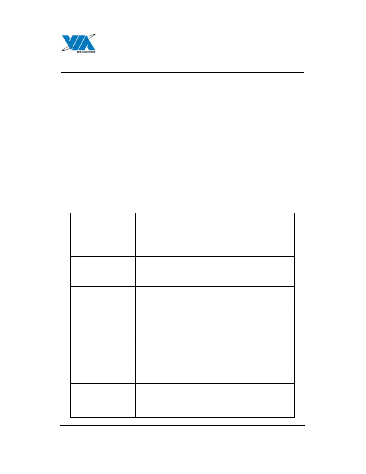
3.5 FIR Module Connector (Reference Designs for FIR module available):
Power LED
HDD LED
Power
Switch
Reset
J3
1
2
11
12
4 Ground
5 IRTX
3 IRRX2
2 IRRX
J5
1 +3V
Page 5

VIA Technologies, Inc. VIA EPIA Mini-ITX Mainboard
Operation Guidelines
-5-
3.6 CIR Module Connector (Reference Designs for CIR module available):
3.7 CD-ROM Line-in Connector:
3.8 Wake up on Modem Connector:
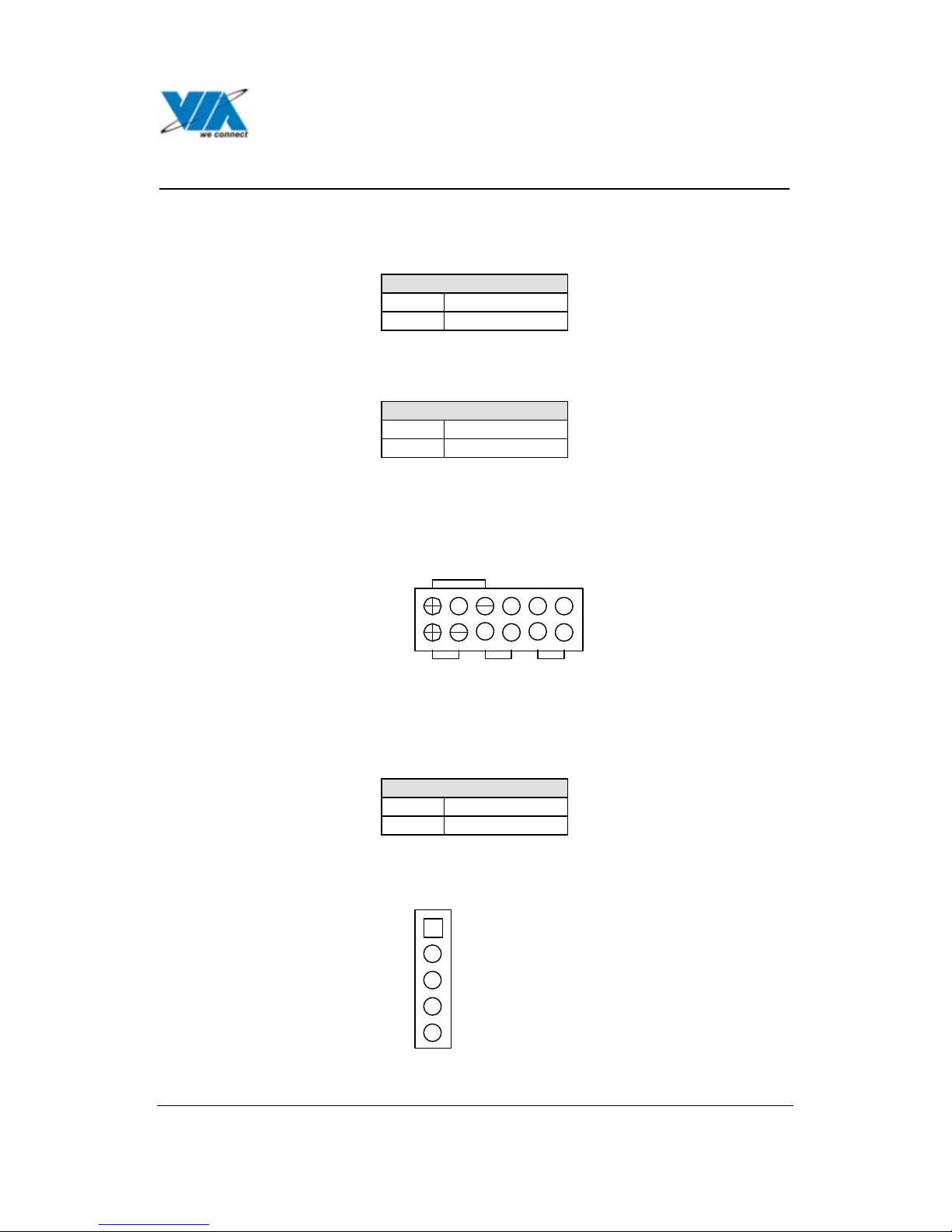
3.9 USB Port 2 & 3 Connector (Reference Design for USB module available):
5 EKBCLK
7 MS_CLK
3 KB_CLK
J6
1 +5V
4 KB_DATA
6 EKBDATA
2 Ground
8 MS_DATA
10 EMDATA
9 EMCLK
3 Ground
J7
4 CD_R
2 Ground
1 CD_L
3 Wake up on Modem
J8
2 Ground
1 5V_SB
6 USB P3 +
4 USB P2 +
3 USB P2 -
J9
1 +5V
7 - OC2
5 USB P3 -
2 Ground
8 -OC3
Page 6

VIA Technologies, Inc. VIA EPIA Mini-ITX Mainboard
Operation Guidelines
-6-
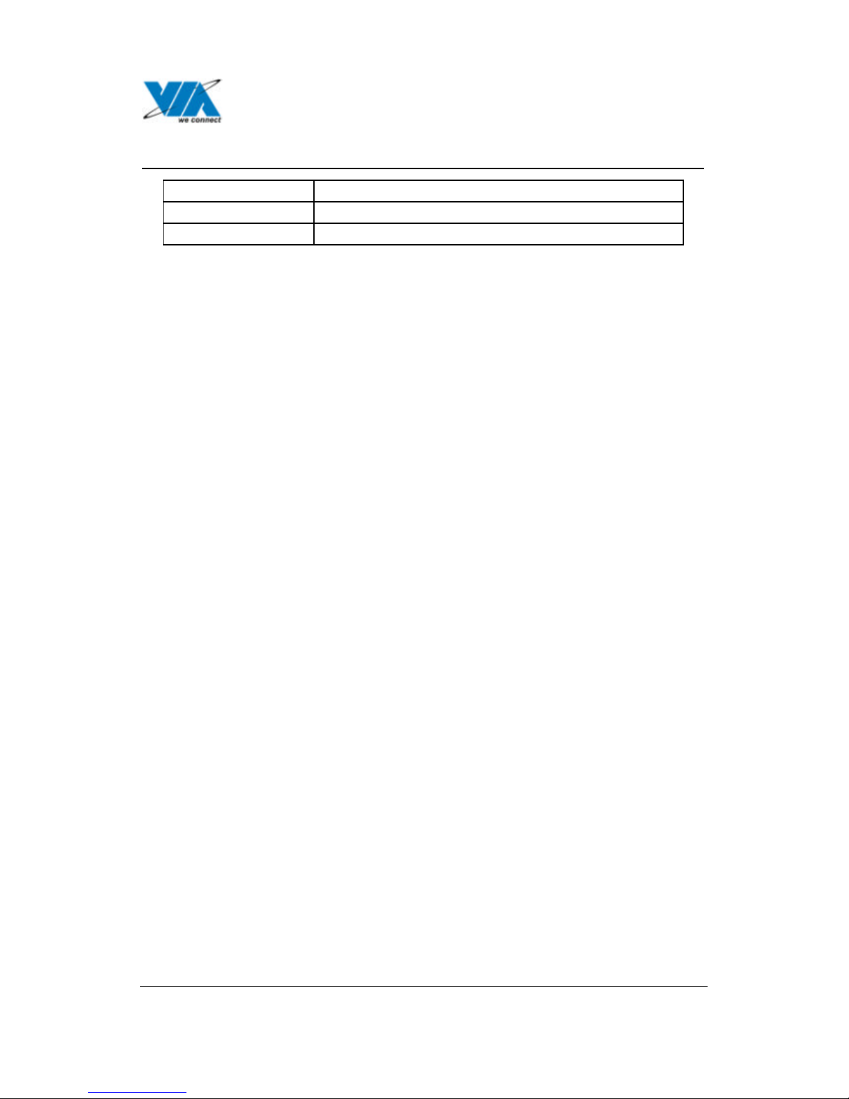
3.10 Clear CMOS:
J10
1-2 Normal
2-3 Clear CMOS
3.11 S/P DIF Output / RCA Video Output Select:
J11
1-2 RCA Video Output
3-4 S/P DIF Output
3.12 VIDEO in Connector (Pins 1-12):
3.12.1 One-to-Two Slot PCI Riser Card Connector (Pins 13, 15, 16 of J12 above)
Reference Design for 1 to 2 slot PCI riser card available
3.13 Host Frequency Select:
J13: Frequency selection for the clock generator jumper setting.
J13
CPU SDRAM PCI
1-2 3-4 5-6 7-8
66 33.33 Open Open Close Close
100 33.33 Open Close Open Close
133 33.33 Close Close Open Open
J12
5 CVD6
7 CVHS
3 CVD7
1 Ground
13 A_D30
15 -GNT2
11 CVVS
9 CVD1
6 CVD5
8 CVD2
4 CVD4
2 CVD0
14 N/A
16 -REQ2
12 CVCLK
10 CVD3
Page 7

VIA Technologies, Inc. VIA EPIA Mini-ITX Mainboard
Operation Guidelines
-7-
4. Connectors:
ITEM FUNCTION
CN1 Audio Connector
CN2 COM Port Connector
CN3 USB Connector and RJ45 Connector
CN4 RCA Video or S/P DIF Jack
CN5 S-Video Jack
CN6 LPT Connector
CN7 CRT Connector
CN8 ATX Power Connector
CN9 PS/2 Keyboard Connector and mouse
Connector
IDE1,IDE2 On-board IDE Primary/Secondary
Connectors
FAN1,FAN2 FAN Connectors
5. Mini-ITX Power Supply
The Mini-ITX compliant power supply is designed with several space, energy and noise reduction
features in mind. The typical physical dimensions (see table below) are very compact compared to
other standard power supplies such as ATX. The options of AC 100 – 240V and 50 – 60Hz auto
switching are fully supported.
Power Supply Length Width Height
Total Area %
smaller
iTX, Mini-ITX 174 mm 73mm 55 mm
ATX 140 mm 150 mm 86 mm 150%
The Mini-ITX power specification uses an industry standard 20-pin main connector to the power
supply as shown below.
1 +3V 11 +3V
2 +3V 12 NC
3 Gnd 13 Gnd
4 +5V 14 PWR_ON-
5 Gnd 15 Gnd
6 +5V 16 Gnd
7 Gnd 17 Gnd
8 PWR_GD 18 NC
9 5V_SB 19 +5V
10 +12V 20 +5V
Note: NC = no connection
1
2
3
4
5
6
7
8
9
11
12
13
14
17
18
19
2010
Page 8

VIA Technologies, Inc. VIA EPIA Mini-ITX Mainboard
Operation Guidelines
-8-
Mini-ITX Switching Power Supply DC Output
Output
Voltage
Load Range Peak 3
Sec.
Voltage
Tolerance
Ripple &
Noise (p-p)
Over Voltage
Protection
Min. Max.
5V_SB 0.1A 1.5A 2.0A ±5% 150mV 6.5V
+3V 0.1A 1.0A 1.5A ±5% 100mV 3.8V
+5V 0.1A 6.0A 7.0A ±5% 100mV 6.5V
+12V 0.1A 0.5A 0.8A ±8% 200mV 15.6V
Total Power: Max 47W, Peak 60W
The VIA EPIA Mini-ITX mainboard leverages its highly efficient architectural design to deliver power
consumption to below one watt when running in optimized low voltage mode.
Page 9

VIA Technologies, Inc. VIA EPIA Mini-ITX Mainboard
Operation Guidelines
-9-
6. Diagrams:
6.1 Layout Placement and Connector Location:
North
Bridge
VT8601ASouth
Bridge
VT8231
C3/Eden
Processor
EBGA
VT1621
TV Out
VT1612A
VT6103
LAN
AC97
Codec
1
ICS
9248
Clock
Generator
DOC
Disk
On
Chip
BIOS
ROM
Buzzer
Battery CR2032
+
-
PS/2
Keyboard
Mouse
LPT Connector
CRT Connector
S-Video
RCA
Video
or
S/P DIF
LAN
RJ-45
USB 1
USB 0
Line
Out
LineInMicInCOM Port
PCI Slot
FAN 1
FAN 2
J11
1-2 RCA Video
* 3-4 S/P DIF
234
J7
CD-ROM Line-in
1
L GG R
J8
Wake up on Modem
1
J10
Clear CMOS
*1-2 Normal
2-3 Clear
1
CIR Module
Connector
J6
1
1
J12
Video in Connector
1
1
J5
FIR Module Connector
1
J4
DOC BIOS
Select
* 1-2 Disable
2-3 Enable
1
J1
CPU Strapping
Function Setting
* 1-2 Disable
2-3 Enable
1
1
J2
Auto Reboot
Function Setting
* 1-2 Disable
2-3 Enable
J3
Panel Jumper
2
11
12
HDD LED
Power SW
Reset SW
Power LED
J9
USB Port 2 & 3 Connector
DIMM 1
DIMM 2
CN8 ATX Power Connector
IDE 1
IDE 2
1
J13 Host Frequency Select
287
--+
+
1-2 3-4 5-6 7-8
66 MHz
100MHz
133MHz
Page 10

VIA Technologies, Inc. VIA EPIA Mini-ITX Mainboard
Operation Guidelines
-10-
6.2 Layout Diagram and Mounting Holes
Page 11

VIA Technologies, Inc. VIA EPIA Mini-ITX Mainboard
Operation Guidelines
-11-
6.3 Back Panel External Connectors:
CN6
LPT
Connector
CN7
CRT
Connector
CN5
S-Video
Jack
CN4
RCA Video
or
S/P DIF
Jack
CN9
Upper
PS/2
Mouse
Connector
CN9
Lower
PS/2
Keyboard
Connector
Line
Out
Line
In
Mic
In
CN2
COM Port
Connector
CN3
Upper
RJ45
Connector
CN1
CN3
Lower
USB
Connector
 Loading...