

Page 1

USER MANUAL
EPIA-M920
Mini-ITX embedded board
1.04-06182013-175200
Page 2

Copyright
Copyright © 2013 VIA Technologies Incorporated. All rights reserved.
No part of this document may be reproduced, transmitted, transcribed, stored in a retrieval system, or translated into any language,
in any form or by any means, electronic, mechanical, magnetic, optical, chemical, manual or otherwise without the prior written
permission of VIA Technologies, Incorporated.
Trademarks
All trademarks are the property of their respective holders.
Disclaimer
No license is granted, implied or otherwise, under any patent or patent rights of VIA Technologies. VIA Technologies makes no
warranties, implied or otherwise, in regard to this document and to the products described in this document. The information
provided in this document is believed to be accurate and reliable as of the publication date of this document. However, VIA
Technologies assumes no responsibility for the use or misuse of the information (including use or connection of extra
device/equipment/add-on card)
The information and product specifications within this document are subject to change at any time, without notice and without
obligation to notify any person of such change.
VIA Technologies, Inc. reserves the right the make changes to the products described in this manual at any time without prior
notice.
Regulatory Compliance
FCC
FCC----A Radio Frequency Interference Statement
A Radio Frequency Interference Statement
FCCFCC
A Radio Frequency Interference StatementA Radio Frequency Interference Statement
This equipment has been tested and found to comply with the limits for a class A digital device, pursuant to part 15 of the FCC
rules. These limits are designed to provide reasonable protection against harmful interference when the equipment is operated in a
commercial environment. This equipment generates, uses, and can radiate radio frequency energy and, if not installed and used in
accordance with the instruction manual, may cause harmful interference to radio communications. Operation of this equipment in a
residential area is likely to cause harmful interference, in which case the user will be required to correct the interference at his
personal expense.
Notice 1
Notice 1
Notice 1Notice 1
The changes or modifications not expressly approved by the party responsible for compliance could void the user's authority to
operate the equipment.
Notice 2
Notice 2
Notice 2Notice 2
Shielded interface cables and A.C. power cord, if any, must be used in order to comply with the emission limits.
Notice 3
Notice 3
Notice 3Notice 3
The product described in this document is designed for general use, VIA Technologies assumes no responsibility for the conflicts
or damages arising from incompatibility of the product. Check compatibility issue with your local sales representatives before
placing an order.
in this document and for any patent infringements that may arise from the use of this document.
Tested To Comply
With FCC Standards
FOR HOME OR OFFICE USE
Page 3

Battery Recycling and Disposal
Only use the appropriate battery specified for this product.
Do not re-use, recharge, or reheat an old battery.
Do not attempt to force open the battery.
Do not discard used batteries with regular trash.
Discard used batteries according to local regulations.
Safety Precautions
Always read the safety instructions carefully.
Keep this User's Manual for future reference.
All cautions and warnings on the equipment should be noted.
Keep this equipment away from humidity.
Lay this equipment on a reliable flat surface before setting it up.
Make sure the voltage of the power source and adjust properly 110/220V before connecting
the equipment to the power inlet.
Place the power cord in such a way that people cannot step on it.
Always unplug the power cord before inserting any add-on card or module.
If any of the following situations arises, get the equipment checked by authorized service
personnel:
The power cord or plug is damaged.
Liquid has penetrated into the equipment.
The equipment has been exposed to moisture.
The equipment has not worked well or you cannot get it work according to User's Manual.
The equipment has dropped and damaged.
The equipment has obvious sign of breakage.
Do not leave this equipment in an environment unconditioned or in a storage temperature
above 60°C (140°F). The equipment may be damaged.
Do not leave this equipment in direct sunlight.
Never pour any liquid into the opening. Liquid can cause damage or electrical shock.
Do not place anything over the power cord.
Do not cover the ventilation holes. The openings on the enclosure protect the equipment
from overheating
Page 4

EPIA
EPIA----M920
EPIAEPIA
Box Contents and Ordering Information
Model Number
Model Number CPU Frequency
Model NumberModel Number
EPIA-M920-10E 1.0GHz Eden™ X2 Standard kit
EPIA-M920-12Q 1.2GHz QuadCore Standard kit
CPU Frequency Description
CPU FrequencyCPU Frequency
Description
DescriptionDescription
1 x SATA cable
1 x I/O bracket
1 x SATA cable
1 x I/O bracket
M920 User Manual
User Manual
M920 M920
User ManualUser Manual
iv
Page 5

EPIA
EPIA----M920
M920 User Manual
EPIAEPIA
M920 M920
Table of Contents
1.
1. Product Overview
Product Overview................................
1.1.
Product OverviewProduct Overview
1.1.
Key Features and Benefits........................................................................... 2
1.1.1. VIA QuadCore /VIA Eden™ X2 Processor ......................................... 2
1.1.2. VIA VX11H MSPIII Chipset.................................................................... 3
1.1.3. Modular Expansion Options................................................................. 3
1.2.
Product Specifications................................................................................. 4
1.3.
Layout Diagram ............................................................................................. 7
1.4.
Product Dimensions..................................................................................... 2
1.5.
Height Distribution....................................................................................... 3
2.
2. I/O Interface
I/O Interface................................
2.2.
I/O InterfaceI/O Interface
2.1.
External I/O Ports ......................................................................................... 5
2.1.1. PS/2 Port.................................................................................................... 6
2.1.2. HDMI® Port............................................................................................... 7
2.1.3. COM Port.................................................................................................. 8
2.1.4. RJ45 LAN port: Gigabit Ethernet ......................................................... 9
2.1.5. Audio Ports.............................................................................................10
2.1.6. VGA Port................................................................................................. 11
2.1.7. USB 2.0 Port ........................................................................................... 12
2.1.8. USB 3.0 Port ........................................................................................... 13
2.2.
Onboard Connectors ................................................................................14
2.2.1. ATX Power Connector......................................................................... 14
2.2.2. LVDS panel connectors ....................................................................... 15
2.2.3. LVDS Inverter Connector ....................................................................18
2.2.4. Digital I/O pin headers ........................................................................ 20
2.2.5. External Thermal Resister.................................................................... 21
2.2.6. Front Panel Pin Header ........................................................................22
2.2.7. SMBus Pin Header................................................................................. 24
2.2.8. CPU and System Fan Connectors ...................................................... 25
2.2.9. SATA Connectors .................................................................................26
................................................................
................................................................
................................................................
................................................................
................................................................
................................................................
................................................................
................................................................
................................ 1111
................................................................
..........................................
................................................................
User Manual
User ManualUser Manual
.......... 5555
....................
v
Page 6

EPIA
2.2.10. USB 2.0 Pin Headers............................................................................. 27
2.2.11. COM Pin Header for COM2~COM4 ................................................ 28
2.2.12. PS/2 Keyboard and Mouse Pin Header ............................................29
2.2.13. Front Audio Pin Header ....................................................................... 30
2.2.14. SPI address select .................................................................................31
2.2.15. SPI Pin Header .......................................................................................32
2.2.16. LPC Pin Header ...................................................................................... 33
2.2.17. SPDIF Connector ................................................................................... 34
2.2.18. CMOS Battery Slot................................................................................ 35
2.2.19. USB3.0 Connector................................................................................. 36
3.
3. Jumpers
Jumpers ................................
3.3.
JumpersJumpers
3.1.
3.2.
3.3.
3.4.
3.4.1. VDD Power Select................................................................................ 41
3.5.
................................................................
................................................................
Clear CMOS Jumper.................................................................................. 37
SATA DOM Power Select Jumper ......................................................... 38
COM1 and COM2 Voltage Select Jumper........................................... 39
COM3 and COM4 Voltage Select Jumper........................................... 40
LVDS Jumper Settings ............................................................................... 42
................................................................
................................................................
...............................................
................................................................
EPIA----M920
M920 User Manual
EPIAEPIA
M920 M920
User Manual
User ManualUser Manual
............... 37
..............................
37
3737
4.
4. Expansion Slots
Expansion Slots................................
4.4.
Expansion SlotsExpansion Slots
4.1.
DDR3 Memory Slots ..................................................................................43
4.1.1. Installing a Memory Module .............................................................. 44
Figure 42: Locking the memory module ...........................................................44
4.1.2. Removing a Memory Module............................................................. 45
4.1.3. PCI Express Slot .................................................................................... 46
5.
5. Hardware Installatio
Hardware Installationnnn ................................
5.5.
Hardware InstallatioHardware Installatio
5.1.
Installing into a Chassis............................................................................. 47
5.1.1. Suggested minimum chassis dimensions ......................................... 47
5.1.2. Suggested minimum chassis height................................................... 48
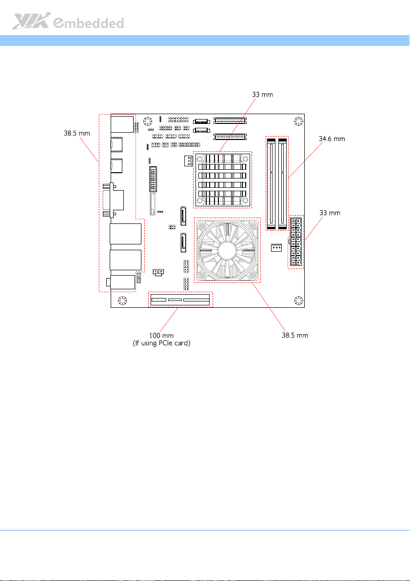
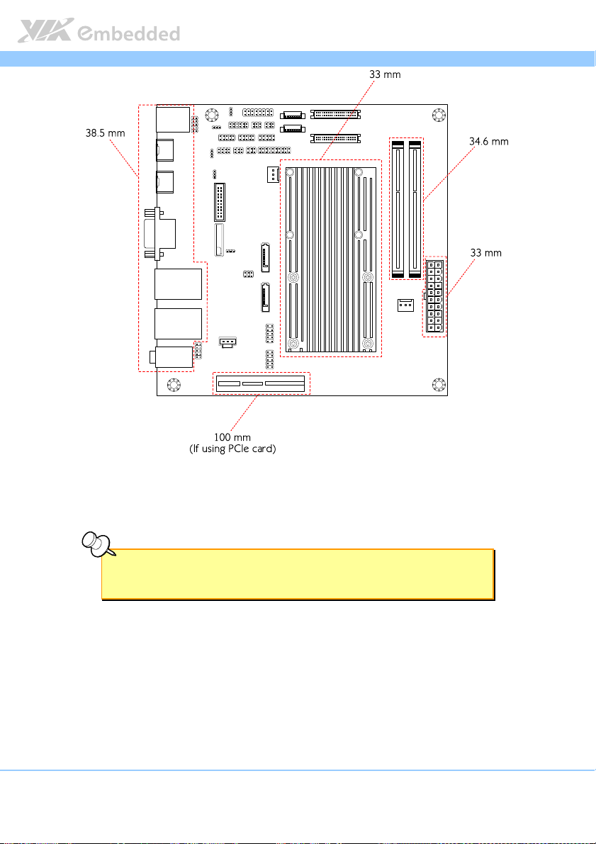
5.1.3. Suggested keepout areas .................................................................... 50
6.
6. BIOS Setup Utility
BIOS Setup Utility................................
6.6.
BIOS Setup UtilityBIOS Setup Utility
................................................................
................................................................
................................................................
................................................................
................................................................
................................................................
................................................................
................................................................
........................................................
................................................................
..............................................................
................................................................
..................................
................................................................
........................ 47
................................................
.............................. 51
............................................................
.. 43
43
....
4343
47
4747
51
5151
vi
Page 7

EPIA
6.1.
Entering the BIOS Setup Utility............................................................... 51
6.2.
Control Keys................................................................................................ 51
6.3.
Navigating the BIOS Menus ..................................................................... 52
6.4.
Getting Help................................................................................................ 52
6.5.
Main Menu ................................................................................................... 53
6.5.1. BIOS Information ................................................................................... 53
6.5.2. Memory Information ............................................................................. 53
6.5.3. System Language................................................................................... 53
6.5.4. System Date............................................................................................ 54
6.5.5. System Time ........................................................................................... 54
6.6.
Advanced Settings ..................................................................................... 55
6.6.1. ACPI Settings.......................................................................................... 56
6.6.2. S5 RTC Wake Settings .......................................................................... 57
6.6.3. CPU Information .................................................................................... 58
6.6.4. SATA Configuration.............................................................................. 59
6.6.5. F71869 Super IO Configuration ......................................................... 60
6.6.6. F71869 H/W Monitor ...........................................................................61
6.6.7. Clock Generator Configuration.......................................................... 62
6.6.8. On Board Configuration ......................................................................63
6.7.
Chipset Settings .......................................................................................... 65
6.7.1. DRAM Configuration ............................................................................66
6.7.2. Video Configuration ............................................................................. 69
6.7.3. UART Configuration.............................................................................. 71
6.7.4. PMU_ACPI Configuration ....................................................................72
6.7.5. HDAC Configuration ............................................................................ 74
6.7.6. SDIO_CR Configuration .......................................................................75
6.7.7. Others Configuration............................................................................ 77
6.8.
Boot Settings ............................................................................................... 78
6.8.1. Boot Configuration................................................................................ 78
6.8.2. Boot Option Priorities ..........................................................................79
6.8.3. Network Device BBS Priorities ...........................................................79
6.9.
Security Settings ......................................................................................... 80
6.9.1. Security Settings .................................................................................... 80
EPIA----M920
M920 User Manual
EPIAEPIA
M920 M920
User Manual
User ManualUser Manual
vii
Page 8

EPIA
6.10. Save & Exit Options ................................................................................... 82
6.10.1. Save Changes and Exit ......................................................................... 82
6.10.2. Discard Changes and Exit.................................................................... 82
6.10.3. Save Changes and Reset...................................................................... 82
6.10.4. Discard Changes and Reset................................................................. 83
6.10.5. Save Changes .........................................................................................83
6.10.6. Discard Changes.................................................................................... 83
6.10.7. VIA Networking Bootagent................................................................. 83
6.10.8. Launch EFI Shell from filesystem device ......................................... 83
7.
7. Driver Installation
Driver Installation................................
7.7.
Driver InstallationDriver Installation
7.1.
Microsoft Driver Support.......................................................................... 85
7.2.
Linux Driver Support.................................................................................. 85
Appendix A. Power Consumption Report
Appendix A. Power Consumption Report................................
Appendix A. Power Consumption ReportAppendix A. Power Consumption Report
A.1. EPIA-M920 Rev. 2 DVT ATX POWER ............................................................ 87
A.1.1. Playing DVD – Power DVD 5.0 ...............................................................87
A.1.2. Playing MP3-Media Player ........................................................................88
A.1.3. Running Network Application ................................................................. 88
A.1.4. IDLE................................................................................................................ 89
A.1.5. RUN Burn-in Test ........................................................................................ 89
A.1.6. S3.................................................................................................................... 90
A.1.7. S5.................................................................................................................... 90
A.1.8. EuP/ErP Enable S3 ......................................................................................91
A.1.9. EuP/ErP Enable S5 ......................................................................................91
................................................................
................................................................
...............................................................
................................................................
...............................................................
................................................................
EPIA----M920
M920 User Manual
M920 M920
User Manual
User ManualUser Manual
EPIAEPIA
............................... 85
..............................................................
............................... 87
..............................................................
85
8585
87
8787
viii
Page 9

EPIA
EPIA----M920
M920 User Manual
EPIAEPIA
M920 M920
User Manual
User ManualUser Manual
Lists of Figures
Figure 1: Layout diagram of the EPIA-M920 mainboard (top view) ...................... 7
Figure 2: Mounting holes and dimensions of the EPIA-M920 mainboard............ 2
Figure 3: External I/O port dimensions of the EPIA-M920 mainboard ................. 2
Figure 4: Height distribution of the EPIA-M920 mainboard (for Quad Core
model) ................................................................................................................................. 3
Figure 5: Height distribution of the EPIA-M920 mainboard (for Dual Core
model) ................................................................................................................................. 4
Figure 6: External I/O ports............................................................................................. 5
Figure 7: PS/2 port pinout diagram ............................................................................... 6
Figure 8: HDMI® port pinout diagram........................................................................... 7
Figure 9: COM port pinout diagram.............................................................................. 8
Figure 10: Gigabit Ethernet port pinout diagram ....................................................... 9
Figure 11: Audio jack receptacle stack....................................................................... 10
Figure 12: VGA port pinout diagram ..........................................................................11
Figure 13: USB port pinout diagram............................................................................ 12
Figure 14: USB 3.0 port pinout diagram..................................................................... 13
Figure 15: ATX power connector ................................................................................14
Figure 16: LVDS panel connector................................................................................ 15
Figure 17: LVDS Inverter connector ............................................................................ 18
Figure 18: Digital I/O pin headers ............................................................................... 20
Figure 19: External Thermal Resister........................................................................... 21
Figure 20: Front panel pin header ............................................................................... 22
Figure 21: SMBus pin header ........................................................................................ 24
Figure 22: CPU and System Fan connectors ..............................................................25
Figure 23: SATA connectors ......................................................................................... 26
Figure 24: USB pin headers ........................................................................................... 27
Figure 25: COM pin headers......................................................................................... 28
Figure 26: PS/2 keyboard and mouse pin header .................................................... 29
Figure 27: Front audio pin header ...............................................................................30
Figure 28: SPI address select ........................................................................................ 31
Figure 29: SPI pin header ............................................................................................... 32
ix
Page 10

EPIA
Figure 30: LPC pin header.............................................................................................. 33
Figure 31: SPDIF connector ...........................................................................................34
Figure 32: CMOS battery slot ....................................................................................... 35
Figure 33: USB 3.0 connectors .....................................................................................36
Figure 34: CLEAR CMOS jumper .................................................................................37
Figure 35: SATA DOM voltage select jumper.......................................................... 38
Figure 36: COM1 and COM2 voltage select jumper .............................................. 39
Figure 37: COM3 and COM4 voltage select jumper .............................................. 40
Figure 38: VDD Power Select....................................................................................... 41
Figure 39: LVDS jumper settings ..................................................................................42
Figure 40: DDR3 memory slots ....................................................................................43
Figure 41: Inserting the memory module................................................................... 44
Figure 42: Locking the memory module .................................................................... 44
Figure 43: Disengaging the SODIMM locking clips ................................................. 45
Figure 44: Removing the memory module ................................................................ 45
Figure 45: PCI Express slot ............................................................................................ 46
Figure 46: Suggested minimum chassis dimensions ................................................ 47
Figure 47: Suggested minimum internal chassis ceiling height (for dual core
model) ............................................................................................................................... 48
Figure 48: Suggested minimum internal chassis ceiling height (for quad core
model) ............................................................................................................................... 49
Figure 49: Suggested keepout areas ........................................................................... 50
Figure 50: Illustration of the Main menu screen....................................................... 53
Figure 51: Illustration of the Advanced Settings screen......................................... 55
Figure 52: Illustration of the ACPI Settings screen .................................................. 56
Figure 53: Illustration of S5 RTC Wake Settings screen.......................................... 57
Figure 54: Illustration of CPU Information screen .................................................... 58
Figure 55: Illustration of SATA Configuration screen ............................................. 59
Figure 56: Illustration of F71869 Super IO Configuration screen......................... 60
Figure 57: Illustration of F71869 H/W Monitor screen ........................................... 61
Figure 58: Illustration of Clock Generator Configuration screen ......................... 62
Figure 59: Illustration of On Board Configuration screen...................................... 63
Figure 60: Illustration of Chipset Settings screen..................................................... 65
EPIA----M920
M920 User Manual
EPIAEPIA
M920 M920
User Manual
User ManualUser Manual
x
Page 11

EPIA
Figure 61: Illustration of DRAM Configuration screen ............................................ 66
Figure 62: Illustration of Video Configuration screen .............................................69
Figure 63: Illustration of UART Configuration screen .............................................71
Figure 64: Illustration of PMU_ACPI Configuration screen.................................... 72
Figure 65: Illustration of Other Control screen........................................................ 73
Figure 66: Illustration of HDAC Configuration screen............................................ 74
Figure 67: Illustration of SDIO_CR Configuration screen....................................... 75
Figure 68: Illustration of Others Configuration screen ...........................................77
Figure 69: Illustration of Boot Settings screen.......................................................... 78
Figure 70: Illustration of Security Settings screen.................................................... 80
Figure 71: Illustration of Save & Exit Options screen .............................................82
EPIA----M920
M920 User Manual
EPIAEPIA
M920 M920
User Manual
User ManualUser Manual
xi
Page 12

EPIA
EPIA----M920
M920 User Manual
EPIAEPIA
M920 M920
User Manual
User ManualUser Manual
Lists of Tables
Table 1: PS/2 port pinout ................................................................................................ 6
Table 2: HDMI® port pinout ........................................................................................... 7
Table 3: COM port pinout .............................................................................................. 8
Table 4: Gigabit Ethernet port pinout .......................................................................... 9
Table 5: Gigabit Ethernet LED color definition .......................................................... 9
Table 6: Audio jack receptacle pinout....................................................................... 10
Table 7: VGA port pinout ............................................................................................. 11
Table 8: USB port pinout............................................................................................... 12
Table 9: USB 3.0 port pinout........................................................................................ 13
Table 10: ATX power connector pinout ...................................................................14
Table 11: LVDS1 panel pinout ..................................................................................... 16
Table 12: LVDS2 panel pinout ..................................................................................... 17
Table 13: LVDS Inverter connector pinout................................................................ 19
Table 14: Digital I/O pin headers pinout................................................................... 20
Table 15: External thermal resister pinout................................................................ 21
Table 16: Front panel pin header pinout................................................................... 23
Table 17: SMBus pin header pinout............................................................................ 24
Table 18: CPU and System Fan connector pinouts .................................................25
Table 19: SATA connector pinouts............................................................................. 26
Table 20: USB pin header pinouts............................................................................... 27
Table 21: COM pin header pinout .............................................................................. 28
Table 22: PS/2 keyboard and mouse pin header pinout ........................................ 29
Table 23: Front audio pin header pinout................................................................... 30
Table 24: SPI address select pinout............................................................................ 31
Table 25: SPI pin header pinout ..................................................................................32
Table 26: LPC pin header pinout ................................................................................. 33
Table 27: SPDIF connector pinout ..............................................................................34
Table 28: CMOS battery slot pinout .......................................................................... 35
Table 29: USB 3.0 connector pinout........................................................................... 36
Table 30: CLEAR CMOS jumper settings ................................................................... 37
Table 31: SATA DOM voltage select jumper settings ........................................... 38
xii
Page 13

EPIA
Table 32: COM1 and COM2 voltage select jumper settings ...............................39
Table 33: COM3 and COM4 voltage select jumper settings ...............................40
Table 34: VDD Power Select pinout .......................................................................... 41
Table 35: LVDS jumper settings................................................................................... 42
EPIA----M920
M920 User Manual
EPIAEPIA
M920 M920
User Manual
User ManualUser Manual
xiii
Page 14

EPIA
1.
1. Product Overview
Product Overview
1.1.
Product OverviewProduct Overview
The VIA EPIA-M920 Mini-ITX mainboard is a high performance native x86
mainboard designed mainly for embedded, POS, Kiosk, ATM and digital media
application. It can also be used for various domain applications such as
desktop PC, industrial PC, etc. The mainboard is based on the VIA VX11H
MSPIII (Media System Processor) chipset that features the VIA Chrome
DX11 with 2D/3D graphics and video accelerators for rich digital media
performance.
The VIA EPIA-M920 includes a powerful, secure, and efficient VIA Eden
VIA QuadCore processor. The VIA Eden
Padlock Security Engine, VIA CoolStream
Technology Suite, and VIA TwinTurbo
QuadCore processor includes the VIA AES Security Engine, VIA CoolStream
Architecture and VIA PowerSaver
The VIA EPIA-M920 has two 1333 MHz DDR3 SODIMM slots that support up
to 16 GB memory size. The VIA EPIA-M920 provides support for high fidelity
audio with its included VIA VT2021 High Definition Audio Codec. In addition
it supports two SATA 3Gb/s storage devices.
™
X2 processor includes the VIA
™
Architecture, VIA StepAhead™
™
technology. Whereas the VIA
™
Technology.
EPIA----M920
M920 User Manual
EPIAEPIA
M920 M920
User Manual
User ManualUser Manual
™
640
™
X2 /
™
The VIA EPIA-M920 is compatible with a full range of Mini-ITX chassis as well
as FlexATX and MicroATX enclosures and power supplies. The VIA EPIA-
®
M920 is fully compatible with Microsoft
and Linux operating systems.
1
Page 15
EPIA
EPIA----M920
EPIAEPIA
1.1. Key Features and Benefits
M920 User Manual
User Manual
M920 M920
User ManualUser Manual
1.1.1. VIA QuadCore /VIA Eden
™
X2 Processor
The VIA QuadCore is a 64-bit superscalar x86 quad core (Isaiah) processor
combine on two dies. It is based on advanced 40 nanometer process
technology packed into an ultra compact NanoBGA2 package measuring
21mm x 21mm. The VIA QuadCore processor delivers a superb performance
on multi-tasking, multimedia playback, productivity and internet browsing in a
low power budget.
The VIA Eden X2 is a 64-bit superscalar x86 dual core processor based on a
40 nanometer process technology. Packed into an ultra compact NanoBGA2
package (measuring 21mm x 21mm), it delivers an energy-efficient yet
powerful performance, with cool and quiet operation.
Note:
Note:
Note:Note:
For Windows 7 and Windows Server 2008 R2 users only:
If encounter the issue such as the operating system recognize the VIA Dual-Core CPU as two processors
instead of one processor with two cores. Download and install the hotfix released by Microsoft to
address this issue. The downloadable hotfix is available at http://support.microsoft.com/kb/2502664
http://support.microsoft.com/kb/2502664
http://support.microsoft.com/kb/2502664http://support.microsoft.com/kb/2502664
Both VIA QuadCore and Eden X2 processors are ideal for embedded system
applications such as industrial PCs, test machines, measuring equipment,
digital signage, medical PCs, monitoring systems, gaming machines, in-vehicle
entertainment, etc.
2
Page 16

EPIA
EPIA----M920
M920 User Manual
EPIAEPIA
M920 M920
User Manual
User ManualUser Manual
1.1.2. VIA VX11H MSPIII Chipset
The VIA VX11H is the fourth generation, highly integrated Media System
Processor which provides high quality digital video streaming and high
definition video playback. It features the VIA Chrome
graphics and video processor, High Definition video decoder
™
640 DX11 2D/3D
and supports
DDR3 1333 controller and USB 3.0 interface.
The VIA VX11H offers superb-graphics performance, immersive visual
experience, and supports DirectX 11.0 that allows realistic 3D rendering and
increased visual acuity. It is also based on a highly sophisticated power
efficient architecture that enables such rich integration into a compact package.
1.1.3. Modular Expansion Options
The VIA EPIA-M920 ensures long-term usability with its support for industry
standard expansion options. Its support for legacy PCI expansion cards helps
to smooth and reduce the costs of transitioning to newer expansion
technologies. The VIA EPIA-M920 enables companies to slowly roll out
upgrades as necessary instead of having to replace everything all at once. This
ensures that companies using the EPIA-M920 obtain the maximum benefits
from its past investments in PCI expansion cards.
The VIA EPIA-M920 also includes a 4-Lane PCI Express 2.0 expansion slot that
provides protection against obsolescence.
3
Page 17
EPIA
EPIA----M920
EPIAEPIA
1.2. Product Specifications
Processor
Processor
ProcessorProcessor
VIA Nano X4 1.2GHz+ with fansink (27.5W)
VIA Eden X2 1.0GHz+ fanless
7 bit VID
Chipset
Chipset
ChipsetChipset
VIA VX11H MSPIII 33 x 33mm
System Memory
System Memory
System MemorySystem Memory
2 x DDR3 1333 SODIMM
Supports up to 16 GB memory size
Note:
Note:
Note:Note:
The real memory size may show less than 16GB due to some capacity are used for BIOS or other
functions.
VGA
VGA
VGAVGA
Integrated VIA Chrome™ 640 HD DX11 3D/2D graphics with MPEG2, WMV9/VC1,
H.264 decoding acceleration
Onboard
Onboard Peripherals
Onboard Onboard
Onboard I/O Connectors
Onboard I/O Connectors
Onboard I/O ConnectorsOnboard I/O Connectors
Peripherals
PeripheralsPeripherals
Serial
Serial ATA
ATA
Serial Serial
ATAATA
2 SATA connectors
Onboard LAN
Onboard LAN
Onboard LANOnboard LAN
2 x VIA VT6130 PCIe Gigabit Ethernet Controller
Onboard Audio
Onboard Audio
Onboard AudioOnboard Audio
VIA VT2021 High Definition Audio Codec
Onboard Super I
Onboard Super I////OOOO
Onboard Super IOnboard Super I
Fintek F71869E
2 x USB 2.0 pin headers for 4 ports
1 x USB3.0 pin header for 1 port
2 x SATA connectors
2 x SATA DOM Power selectors
1 x Dual channel 18/24-bit LVDS (DVP, VT1636)
1 x Single channel 18/24-bit LVDS (VX11H internal)
2 x Backlight control connectors for inverter power and brightness control
M920 User Manual
User Manual
M920 M920
User ManualUser Manual
4
Page 18

EPIA
1 x Front audio pin header (Line-out/MIC-in)
1 x PS/2 keyboard/mouse pin header
3 x RS232 pin header (2 from VX11H, configurable 5V/12V)
1 x LPC pin header
1 x SMBus pin header
1 x S/PDIF Out connector
1 x Digital I/O pin headers (GPI x 4, GPO x 4)
1 x Front panel pin header
2 x Smart Fan pin headers for CPU and System
1 x ATX power connector
1 x PCIex4 slot
1 x SD card (SDHC/SDXC)
1 x SPI
1 x Clear CMOS
EPIA----M920
EPIAEPIA
Back Panel I/O
Back Panel I/O
Back Panel I/OBack Panel I/O
1 x Serial port (powered with selectable 5V/12V) + VGA port
2 x HDMI® ports
1 x GigaLAN port + 2 x USB3.0 ports
1 x GigaLAN port + 2 x USB2.0 ports
3 x Audio jacks: Line-in, Line-out and MIC-in
2 x PS/2 KB/MS ports
I/O Bracket
I/O Bracket
I/O BracketI/O Bracket
Standard
BIOS
BIOS
BIOSBIOS
AMI BIOS ROM APTIO uEFI 4MB
Operating System
Operating System
Operating SystemOperating System
Windows 7
Windows Embedded Standard 7
Windows Embedded POSReady 7
Windows XP
Windows Embedded Standard
Linux
Power
Power
PowerPower
ATX Power connector
M920 User Manual
User Manual
M920 M920
User ManualUser Manual
5
Page 19

EPIA
System Monitoring & Management
System Monitoring & Management
System Monitoring & ManagementSystem Monitoring & Management
Wake-on-LAN
Keyboard Power-on
Timer Power-on
System power management
AC power failure recovery
Watch Dog Timer
EPIA----M920
EPIAEPIA
Operating Conditions
Operating Conditions
Operating ConditionsOperating Conditions
Operating Temperature
Operating Temperature
Operating TemperatureOperating Temperature
0°C up to 60°C
Operating Humidity
Operating Humidity
Operating HumidityOperating Humidity
0% ~ 95% (relative humidity; non-condensing)
Form Factor
Form Factor
Form FactorForm Factor
Mini-ITX (8-layer)
17 cm x 17 cm
Compliance
Compliance
ComplianceCompliance
CE
FCC
BSMI
RoHS
M920 User Manual
User Manual
M920 M920
User ManualUser Manual
6
Page 20
EPIA
EPIA----M920
EPIAEPIA
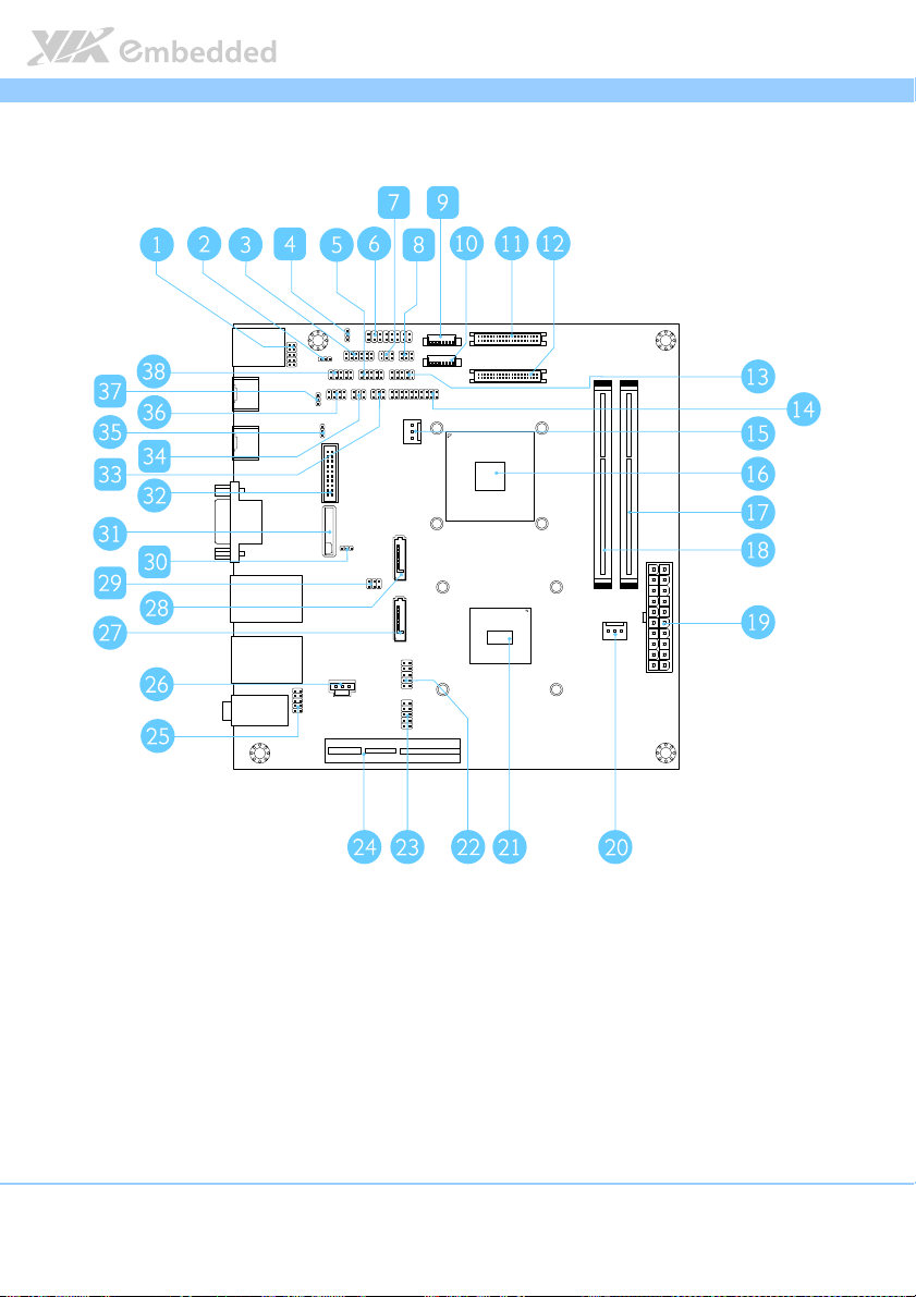
1.3. Layout Diagram
M920 User Manual
User Manual
M920 M920
User ManualUser Manual
Figure
Figure 1111: Layout diagram of the
: Layout diagram of the EPIA
Figure Figure
: Layout diagram of the : Layout diagram of the
EPIA----M920
M920 mainboard
EPIAEPIA
M920M920
mainboard (top view)
mainboard mainboard
(top view)
(top view) (top view)
7
Page 21

EPIA
Item
Item Description
ItemItem
1 PS/2 keyboard and mouse pin header (JKBMS)
2 SMBus pin header (SMBUS1)
3 Digital I/O pin headers (DIO1)
4 VDD Power Select jumper (J9)
5 COM4 pin header
6 Front panel pin header (F_PANEL)
7 LVDS1 power select jumper (J14)
8 LVDS2 power select jumper (J15)
9 LVDS inverter connectors (INVERTER2)
10 LVDS inverter connectors (INVERTER1)
11 LVDS connectors (LVDS2)
12 LVDS connectors (LVDS1)
13 COM3 pin header
14 LPC pin header (LPC1)
15 System fan connector (SYSFAN)
16 VIA VX11H chipset
17 Memory slots (SODIMM2)
18 Memory slots (SODIMM1)
19 ATX power supply connector (ATX_POWER2)
20 CPU fan Connector (CPUFAN)
21 VIA Nano X4/ VIA Eden X2 CPU
22 USB pin header (USB_1)
23 USB pin header (USB_2)
24 PCIE x4 slot
25 Front audio pin header (F_AUDIO1)
26 SPDIF connector (SPDIF1)
27 SATA connector (SATA1)
28 SATA connector (SATA2)
29 SATA DOM power select jumper (J12)
30 Clear CMOS jumper (J10)
31 CMOS battery socket (BAT1)
32 USB3.0 Connector (J8)
33 COM3 and COM4 Voltage Select Jumper (J13)
34 COM1 and COM2 Voltage Select Jumper (J11)
35 External Thermal Resister jumper (J7)
36 SPI1 pin header
37 SPI Address Select jumper (J6)
38 COM2 pin header
Description
DescriptionDescription
EPIA----M920
EPIAEPIA
M920 User Manual
User Manual
M920 M920
User ManualUser Manual
1
Page 22
EPIA
EPIA----M920
EPIAEPIA
1.4. Product Dimensions
Figure
Figure 2222: Mounting holes an
: Mounting holes and dimensions of the
Figure Figure
: Mounting holes an: Mounting holes an
d dimensions of the EPIA
d dimensions of the d dimensions of the
EPIA----M920
EPIAEPIA
M920 mainboard
mainboard
M920M920
mainboard mainboard
M920 User Manual
User Manual
M920 M920
User ManualUser Manual
Unit: mm
Figure
Figure 3333:
: External
External I/O
I/O port
port dimensions of the
Figure Figure
: :
External External
dimensions of the EPIA
I/O I/O
portport
dimensions of the dimensions of the
EPIA----M920
M920 mainboard
EPIAEPIA
M920M920
mainboard
mainboard mainboard
2
Page 23
EPIA
EPIA----M920
EPIAEPIA
1.5. Height Distribution
M920 User Manual
User Manual
M920 M920
User ManualUser Manual
Figure
Figure 4444: Height distribution of the
: Height distribution of the EPIA
Figure Figure
: Height distribution of the : Height distribution of the
EPIA----M920
M920 mainboard
EPIAEPIA
M920M920
mainboard (for
mainboard mainboard
(for Qu
(for(for
Quad Core model
ad Core model))))
Qu Qu
ad Core modelad Core model
3
Page 24
EPIA
Figure
Figure 5555: Height distribution of the EPIA
: Height distribution of the EPIA----M920
Figure Figure
: Height distribution of the EPIA: Height distribution of the EPIA
M920 mainboard
mainboard (for
M920M920
mainboard mainboard
(for Dual Core model
Dual Core model))))
(for(for
Dual Core model Dual Core model
EPIA----M920
EPIAEPIA
M920 User Manual
User Manual
M920 M920
User ManualUser Manual
Note:
Note:
Note:Note:
All other heights are under 21.00 mm.
4
Page 25
EPIA
2.
2. I/O Interface
I/O Interface
2.2.
I/O InterfaceI/O Interface
The VIA EPIA-M920 has a wide selection of interfaces integrated into the
board. It includes a selection of frequently used ports as part of the external
I/O coastline.
EPIA----M920
M920 User Manual
EPIAEPIA
M920 M920
User Manual
User ManualUser Manual
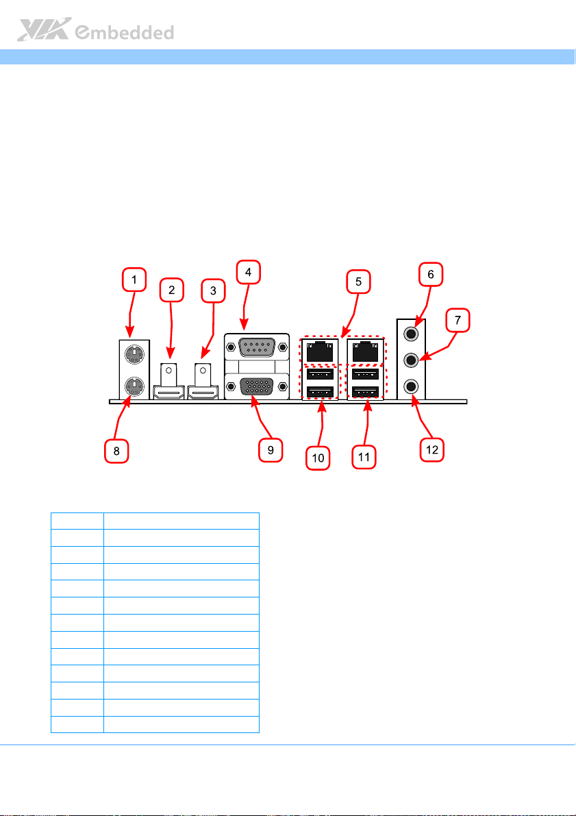
2.1. External I/O Ports
Figure
Figure 6666: External I/O ports
: External I/O ports
Figure Figure
: External I/O ports: External I/O ports
Item
Item Description
ItemItem
1 PS/2 mouse port
2 HDMI1 port
3 HDMI2 port
4 COM1 port
5 Gigabit Ethernet ports
6 Line-in 3.5 mm TRS jack
7 Line-out 3.5 mm TRS jack
8 PS/2 keyboard port
9 VGA port
10 USB 3.0 ports
11 USB 2.0 ports
12 Microphone 3.5 mm TRS jack
Description
DescriptionDescription
5
Page 26
EPIA
EPIA----M920
M920 User Manual
EPIAEPIA
M920 M920
User Manual
User ManualUser Manual
2.1.1. PS/2 Port
The mainboard has two integrated PS/2 ports for keyboard and mouse. Each
port is using the 6-pin Mini-DIN connector. The color purple is used for a PS/2
keyboard while the color green is used for a PS/2 mouse. The pinout of the
PS/2 port are shown below.
Pin
Pin
Signal
Signal
PinPin
SignalSignal
1 Data
2 NC
3 Ground
4 +5V
5 Clock
6 NC
Table
Table 1111: PS/2 port pinout
: PS/2 port pinout
TableTable
: PS/2 port pinout: PS/2 port pinout
Figure
Figure 7777:
Figure Figure
: PS/2
PS/2 port pinout diagram
: :
PS/2PS/2
5
6
34
12
port pinout diagram
port pinout diagram port pinout diagram
6
Page 27
EPIA
EPIA----M920
EPIAEPIA
M920 User Manual
User Manual
M920 M920
User ManualUser Manual
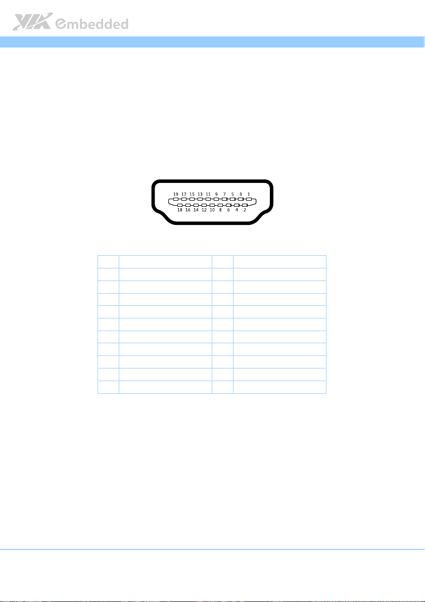
2.1.2. HDMI
®
Port
The integrated 19-pin HDMI® port uses an HDMI® Type A receptacle
®
connector as defined in the HDMI
specification. The HDMI® (High Definition
Multimedia Interface) port is for connecting the high definition video and
digital audio. It allows you to connect the digital video devices which utilize a
high definition video signal. The pinout of the HDMI
®
port is shown below.
Figure
Figure 8888: HDMI
Figure Figure
Ta
Table
ble 2222: HDMI
TaTa
ble ble
®®®®
: HDMI
port pinout diagram
port pinout diagram
: HDMI: HDMI
port pinout diagram port pinout diagram
®®®®
: HDMI
port pinout
port pinout
: HDMI: HDMI
port pinout port pinout
Pin
Pin
Signal
Signal Pin
PinPin
SignalSignal
1 TX2+ 2 Ground
3 TX2- 4 TX1+
5 Ground 6 TX1-
7 TX0+ 8 Ground
9 TX0- 10 TXC+
11 Ground 12 TXC-
13 key 14 key
15 DDCSCL 16 DDCSDA
17 Ground 18 +5V
19 Hot Plug Detect
Pin
PinPin
Signal
Signal
SignalSignal
7
Page 28
EPIA
EPIA----M920
M920 User Manual
EPIAEPIA
M920 M920
User Manual
User ManualUser Manual
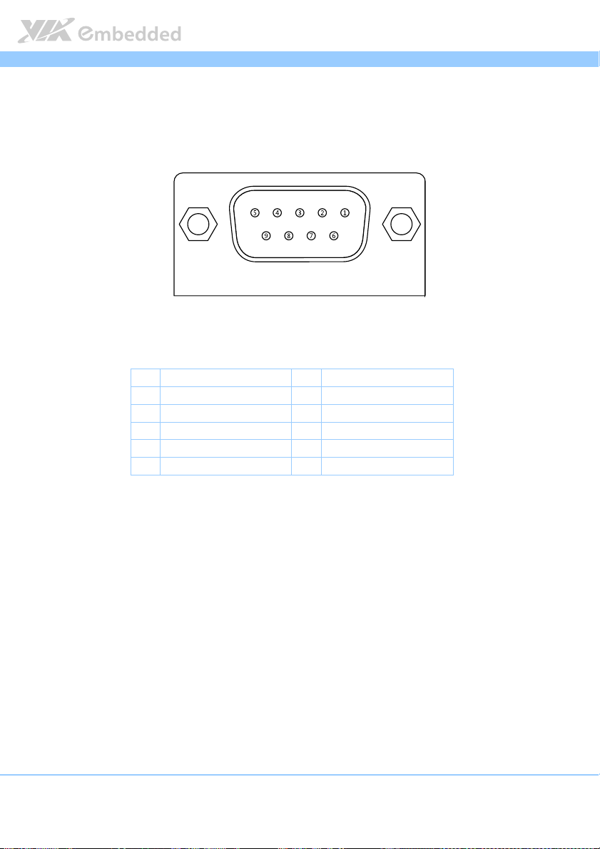
2.1.3. COM Port
The integrated 9-pin COM port uses a male DE-9 connector. The COM
(COM1) port supports the RS-232 standard. The pinout of the COM port is
shown below.
Figure
Figure 9999: CO
: COM port pinout diagram
Figure Figure
Table
Table 3333:
Table Table
M port pinout diagram
: CO: CO
M port pinout diagramM port pinout diagram
Pin
Pin
Signal
Signal Pin
PinPin
SignalSignal
1 DCD 6 DSR
2 RxD 7 RTS
3 TxD 8 CTS
4 DTR 9 RI
5 GND
: COM port pinout
COM port pinout
: :
COM port pinoutCOM port pinout
Pin
PinPin
Signal
Signal
SignalSignal
8
Page 29
EPIA
EPIA----M920
M920 User Manual
EPIAEPIA
M920 M920
User Manual
User ManualUser Manual
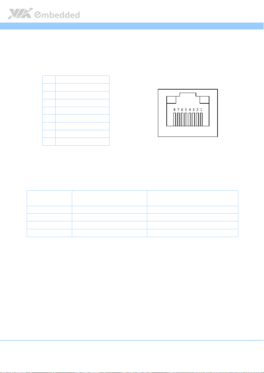
2.1.4. RJ45 LAN port: Gigabit Ethernet
The integrated 8-pin Gigabit Ethernet port is using an 8 Position 8 Contact
(8P8C) receptacle connector (commonly referred to as RJ45). The pinout of
the Gigabit Ethernet port is shown below.
Pin
Pin
Signal
Signal
PinPin
SignalSignal
1 Signal pair 1+
2 Signal pair 1-
3 Signal pair 2+
4 Signal pair 3+
5 Signal pair 3-
6 Signal pair 2-
7 Signal pair 4+
8 Signal pair 4-
Table
Table 4444: Gigabit Ethernet port pinout
: Gigabit Ethernet port pinout
Table Table
: Gigabit Ethernet port pinout: Gigabit Ethernet port pinout
Figure
Figure 10
10: Gigabit Ethernet port pinout diagram
Figure Figure
There are two RJ-45 ports and each port has two individual LED indicators
located on the front side to show its Active/Link status and Speed status.
: Gigabit Ethernet port pinout diagram
1010
: Gigabit Ethernet port pinout diagram: Gigabit Ethernet port pinout diagram
Active LED
(Left LED on RJ
(Left LED on RJ----45 connector)
(Left LED on RJ(Left LED on RJ
Link Off Off The LED is always On in Orange color
Speed_10Mbit Flash in Green color The LED is always On in Orange color
Speed_100Mbit Flash in Green color The LED is always On in Green color
Speed_1000Mbit Flash in Green color The LED is always On in Red color
Table
Table 5555: Gigabit Ethernet LED color de
: Gigabit Ethernet LED color definition
Table Table
: Gigabit Ethernet LED color de: Gigabit Ethernet LED color de
Active LED
Active LEDActive LED
45 connector)
45 connector)45 connector)
finition
finitionfinition
Link LED
Link LED
Link LEDLink LED
(Right LED on RJ
(Right LED on RJ----45 connector)
(Right LED on RJ(Right LED on RJ
45 connector)
45 connector)45 connector)
9
Page 30
EPIA
EPIA----M920
M920 User Manual
EPIAEPIA
M920 M920
User Manual
User ManualUser Manual
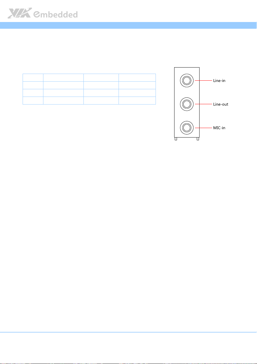
2.1.5. Audio Ports
There are three audio jack receptacles integrated into a single stack on the I/O
coastline. Each receptacle can fit a 3.5 mm Tip Ring Sleeve (TRS) connector to
enable connections to Line-in, Line-out, and MIC-in.
Wiring
Wiring
WiringWiring
Tip Left channel in Left channel Left channel
Ring Right channel in Right channel Right channel
Sleeve Ground Ground Ground
Table
Table 6666: Audio jack receptacle pinout
Table Table
Line
Line----in
in Line
LineLine
inin
: Audio jack receptacle pinout
: Audio jack receptacle pinout: Audio jack receptacle pinout
Line----out
out MIC
LineLine
outout
MIC----in
MICMIC
in
inin
Figure
Figure 11
Figure Figure
11: Audio jack receptacle stack
1111
: Audio jack receptacle stack
: Audio jack receptacle stack: Audio jack receptacle stack
10
Page 31

EPIA
EPIA----M920
M920 User Manual
EPIAEPIA
M920 M920
User Manual
User ManualUser Manual
2.1.6. VGA Port
The integrated 15-pin VGA port uses a female DE-15 connector. The VGA
port is for connecting to analog displays. The pinout of the VGA port is shown
below.
Figure
Figure 12
12: VGA port pinout diagram
Figure Figure
Table
Table 7777: VGA port pinout
Table Table
: VGA port pinout diagram
1212
: VGA port pinout diagram: VGA port pinout diagram
Pin
Pin
Signal
Signal
PinPin
SignalSignal
1 RED
2 GREEN
3 BLUE
4 NC
5 Ground
6 Ground
7 Ground
8 Ground
9 +5V
10 NC
11 NC
12 SDA
13 HSync
14 VSync
15 SCL
: VGA port pinout
: VGA port pinout: VGA port pinout
11
Page 32

EPIA
EPIA----M920
M920 User Manual
EPIAEPIA
M920 M920
User Manual
User ManualUser Manual
2.1.7. USB 2.0 Port
There are two integrated USB 2.0 ports in EPIA-M920 mainboard. The USB-
interface port gives complete Plug and Play and hot swap capability for
external devices and it complies with USB UHCI, rev. 2.0. Each USB port is
using the USB Type A receptacle connector. The pinout of the typical USB
port is shown below.
Pin
Pin
Signal
Signal
PinPin
SignalSignal
1 +5VSUS
2 Data-
3 Data+
4 Ground
Table
Table 8888: USB port pinout
: USB port pinout
Table Table
: USB port pinout: USB port pinout
Figure
Figure 13
13: USB port pinout diagram
Figure Figure
: USB port pinout diagram
1313
: USB port pinout diagram: USB port pinout diagram
12
Page 33

EPIA
EPIA----M920
M920 User Manual
EPIAEPIA
M920 M920
User Manual
User ManualUser Manual
2.1.8. USB 3.0 Port
The EPIA-M920 mainboard provides two USB 3.0 ports, also known as
SuperSpeed USB. The USB 3.0 port has a maximum data transfer rate up to 5
Gbps and offers a backwards compatible with previous USB 2.0 specifications.
The USB 3.0 port is using the USB Type-A receptacle connector. The pinout of
the typical USB 3.0 port is shown below.
Figure
Figure 14
14: USB
: USB 3333.0 port pinout diagram
Figure Figure
1414
Table
Table 9999: USB 3.0 port pinout
Table Table
.0 port pinout diagram
: USB : USB
.0 port pinout diagram.0 port pinout diagram
Pin
Pin
Signal
Signal
PinPin
SignalSignal
1 +5V
2 Data-
3 Data+
4 GND
5 Rx-
6 Rx+
7 GND
8 Tx-
9 Tx+
: USB 3.0 port pinout
: USB 3.0 port pinout: USB 3.0 port pinout
13
Page 34

EPIA
EPIA----M920
M920 User Manual
EPIAEPIA
M920 M920
User Manual
User ManualUser Manual
2.2. Onboard Connectors
2.2.1. ATX Power Connector
The mainboard has a 20-pin ATX power connector onboard. The ATX power
connector is labeled as “ATX_POWER1”. The pinout of the ATX power
connector is shown below.
Figure
Figure 15
15: ATX power connector
Figure Figure
Table
Table 10
Table Table
14
: ATX power connector
1515
: ATX power connector: ATX power connector
Pin
Pin
Signal
Signal Pin
PinPin
SignalSignal
1 +3.3V 11 +3.3V
2 +3.3V 12 -12V
3 Ground 13 Ground
4 +5V 14 PS_ON
5 Ground 15 Ground
6 +5V 16 Ground
7 Ground 17 Ground
8 PW-OK 18 -5V
9 +5VSUS 19 +5V
10 +12V 20 +5V
10: ATX power connector pinout
: ATX power connector pinout
1010
: ATX power connector pinout: ATX power connector pinout
Pin
PinPin
Signal
Signal
SignalSignal
Page 35

EPIA
EPIA----M920
M920 User Manual
EPIAEPIA
M920 M920
User Manual
User ManualUser Manual
2.2.2. LVDS panel connectors
The mainboard has two LVDS panel connectors: LVDS1 and LVDS2. LVDS1
connector is controlled by VIA VX11H chipset while the LVDS2 connector is
controlled by VT1636 LVDS transmitter.
Figure
Figure 16
16: LVDS panel connector
Figure Figure
: LVDS panel connector
1616
: LVDS panel connector: LVDS panel connector
15
Page 36

EPIA
Pin
Pin
Signal
Table
Table 11
11: LVDS1
: LVDS1 panel pinout
Table Table
1111
: LVDS1: LVDS1
Signal Pin
PinPin
SignalSignal
M1 GND
2 PVDD1 1 NC
4 PVDD1 3 NC
6 GND 5 GND
8 GND 7 NC
10 -LD1C0 9 NC
12 +LD1C0 11 GND
14 GND 13 NC
16 -LD1C1 15 NC
18 +LD1C1 17 GND
20 GND 19 NC
22 -LD1C2 21 NC
24 + LD1C2 23 GND
26 GND 25 NC
28 -LCLK1 27 NC
30 + LCLK1 29 NC
32 GND 31 GND
34 -LD1C3 33 NC
36 + LD1C3 35 NC
38 LVDSPCLK 37 NC
40 LPDSPD 39 NC
panel pinout
panel pinoutpanel pinout
Pin
PinPin
Signal
Signal
SignalSignal
EPIA----M920
EPIAEPIA
M920 User Manual
User Manual
M920 M920
User ManualUser Manual
16
Page 37

EPIA
EPIA----M920
EPIAEPIA
Pin
Pin
Signal
Table
Table 12
12: LVD
Table Table
1212
: LVDSSSS2
: LVD: LVD
Signal Pin
PinPin
SignalSignal
M1 GND
2 PVDD2 1 -A4_L
4 PVDD2 3 A4_L
6 GND 5 GND
8 GND 7 -A5_L
10 -A0_L 9 A5_L
12 A0_L 11 GND
14 GND 13 -A6_L
16 -A1_L 15 A6_L
18 A1_L 17 GND
20 GND 19 -CLK2_L
22 -A2_L 21 CLK2_L
24 A2_L 23 GND
26 GND 25 -A7_L
28 -CLK1_L 27 A7_L
30 CLK1_L 29 NC
32 GND 31 NC
34 -A3_L 33 NC
36 A3_L 35 NC
38 DVPSPCLK 37 NC
40 DVPSPD 39 NC
2 panel pinout
panel pinout
2 2
panel pinoutpanel pinout
Pin
PinPin
Signal
Signal
SignalSignal
M920 User Manual
User Manual
M920 M920
User ManualUser Manual
17
Page 38

EPIA
EPIA----M920
M920 User Manual
EPIAEPIA
M920 M920
User Manual
User ManualUser Manual
2.2.3. LVDS Inverter Connector
The mainboard has two inverters for controlling the LVDS panel backlight and
brightness. INVERTER1 corresponds to the LVDS1 panel connector.
INVERTER2 corresponds to the LVDS2 panel connector.
Figure
Figure 17
17: LVDS Inverter connector
Figure Figure
: LVDS Inverter connector
1717
: LVDS Inverter connector: LVDS Inverter connector
18
Page 39

EPIA
Inverter 1
Table
Table 13
13:
: LVDS Inverter connector
Table Table
LVDS Inverter connector pinout
1313
: :
LVDS Inverter connectorLVDS Inverter connector
Inverter 1 Inverter 2
Inverter 1Inverter 1
Pin
Pin
Signal
Signal Pin
PinPin
SignalSignal
1 INV1_12 1 IVDD2
2 INV1_12 2 IVDD2
3 BLON1 3 BAKLITE
4 VX11PWM_CTL1 4 VX11PWM_CTL2
5 BLON1 5 BAKLITE
6 BRIGHTNESS1_CTL1 6 BRIGHTNESS2_CTL2
7 GND 7 GND
8 GND 8 GND
pinout
pinout pinout
Inverter 2
Inverter 2Inverter 2
Pin Signal
Signal
PinPin
SignalSignal
EPIA----M920
EPIAEPIA
M920 User Manual
User Manual
M920 M920
User ManualUser Manual
19
Page 40

EPIA
EPIA----M920
M920 User Manual
EPIAEPIA
M920 M920
User Manual
User ManualUser Manual
2.2.4. Digital I/O pin headers
The mainboard includes one Digital I/O pin header that supports four GPO
and four GPI pins.
Figure
Figure 18
18: Digital I/O pin headers
Figure Figure
Table
Table 14
Table Table
20
: Digital I/O pin headers
1818
: Digital I/O pin headers: Digital I/O pin headers
DIO
DIO 1111
DIO DIO
Pin
Pin
PinPin
1 5V_DIO 2 12V_DIO
3 GPO_37 4 GPI_53
5 GPO_36 6 GPI_52
7 GPO_35 8 GPI_51
9 GPO_34 10 GPI_50
11 GND
14:
: Digital I/O pin headers
Digital I/O pin headers pinout
1414
: :
Digital I/O pin headersDigital I/O pin headers
Signal
Signal Pin
SignalSignal
pinout
pinout pinout
Pin
PinPin
Signal
Signal
SignalSignal
Page 41

EPIA
EPIA----M920
M920 User Manual
EPIAEPIA
M920 M920
User Manual
User ManualUser Manual
2.2.5. External Thermal Resister
The mainboard supports a pin header (3-pin) that allows the connection of a
temperature sensor cable for detecting the system’s internal air temperature.
The temperature reading can be seen in the BIOS Setup Utility. The pin header
is labeled as “J7”. The pinout of the temperature sensor pin header is shown
below.
Figure
Figure 19
19:
: External Thermal Resister
Figure Figure
Table
Table 15
Table Table
External Thermal Resister
1919
: :
External Thermal ResisterExternal Thermal Resister
J7
J7
J7J7
Pin
Pin
Signal
Signal
PinPin
SignalSignal
1 TMPIN2
2 TMPIN2
3 HWMGND
15:
: External thermal resister
External thermal resister pinout
1515
: :
External thermal resister External thermal resister
pinout
pinoutpinout
21
Page 42

EPIA
EPIA----M920
M920 User Manual
EPIAEPIA
M920 M920
User Manual
User ManualUser Manual
2.2.6. Front Panel Pin Header
The front panel pin header consists of 15 pins in a 16-pin block. Pin 15 is
keyed. The front panel pin header is labeled as “F_PANEL1”. It provides access
to system LEDs, power, reset, system speaker and HDD LED. The pinout of the
front panel pin header is shown below.
Figure
Figure 20
20: Front panel pin header
Figure Figure
: Front panel pin header
2020
: Front panel pin header: Front panel pin header
22
Page 43

EPIA
Pin
Pin
Signal
PinPin
1 +5VDUAL 2 +3.3V
3 +5VDUAL 4 SATA_LED
5 PWR_LED 6 PWR_BTN
7 +5V 8 Ground
9 NC 10 -RST_SW
11 NC 12 Ground
13 SPEAK 14 +5V
15
Table
Table 16
16: Front panel pin header pinout
: Front panel pin header pinout
Table Table
1616
: Front panel pin header pinout: Front panel pin header pinout
Signal Pin
SignalSignal
—
Pin
PinPin
16
Signal
Signal
SignalSignal
-SLEEPLED
EPIA----M920
EPIAEPIA
M920 User Manual
User Manual
M920 M920
User ManualUser Manual
23
Page 44

EPIA
EPIA----M920
M920 User Manual
EPIAEPIA
M920 M920
User Manual
User ManualUser Manual
2.2.7. SMBus Pin Header
The SMBus pin header consists of three pins that allow connecting the SMBus
devices. Devices communicate with a SMBus host and/or other SMBus devices
using the SMBus interface. It is labeled as “SMBUS”. The pinout of the SMBus
pin header is shown below.
Pin
Pin
Signal
Signal
PinPin
SignalSignal
1 SMBCK
2 SMBDT
3 Ground
Table
Table 17
17: SMBus pin header
: SMBus pin header pinout
Table Table
1717
: SMBus pin header: SMBus pin header
pinout
pinout pinout
Figure
Figure 21
Figure Figure
21: SMBus pin header
: SMBus pin header
2121
: SMBus pin header: SMBus pin header
24
Page 45

EPIA
EPIA----M920
M920 User Manual
EPIAEPIA
M920 M920
User Manual
User ManualUser Manual
2.2.8. CPU and System Fan Connectors
There are two fan connectors on board: one for the CPU and one for the
chassis. The fan connector for the CPU is labeled as “CPUFAN1” and the fan
connector for the system is labeled as “SYSFAN1”. The fans provide variable
fan speeds controlled by the BIOS. The pinout of the fan connectors is shown
below.
CPU fan (CPUFAN1)
CPU fan (CPUFAN1)
CPU fan (CPUFAN1)CPU fan (CPUFAN1)
Pin
Pin
Signal
Signal
PinPin
SignalSignal
1 F_I01
2 F_PWM1
3 Ground
System fan (SYSFAN1)
System fan (SYSFAN1)
System fan (SYSFAN1)System fan (SYSFAN1)
Pin
Pin
Signal
Signal
PinPin
SignalSignal
1 F_I02
2 F_PWM2
3 Ground
Table
Table 18
18:
: CPU and System
Table Table
CPU and System Fan connector pin
1818
: :
CPU and System CPU and System
Fan connector pinouts
Fan connector pinFan connector pin
outs
outsouts
Figure
Figure 22
Figure Figure
22:
: CPU and System
CPU and System Fan connectors
2222
: :
CPU and System CPU and System
Fan connectors
Fan connectorsFan connectors
25
Page 46

EPIA
EPIA----M920
M920 User Manual
EPIAEPIA
M920 M920
User Manual
User ManualUser Manual
2.2.9. SATA Connectors
The two SATA connectors on board can support up to 3 Gb/s transfer speeds.
The SATA connectors are labeled as “SATA1” and “SATA2”. The pinout of the
SATA connectors are shown below.
SATA1
SATA1
SATA1SATA1
Pin
Pin
Signal
Signal
PinPin
SignalSignal
1 Ground
2 STXP_0
3 STXN_0
4 Ground
5 SRXN_0
6 SRXP_0
7 SATA1_+5V
SATA2
SATA2
SATA2SATA2
Pin
Pin
Signal
Signal
PinPin
SignalSignal
1 Ground
2 STXP_1
3 STXN_1
4 Ground
5 SRXN_1
6 SRXP_1
7 SATA2_+5V
Table
Table 19
19: SATA connect
: SATA connector pinouts
Table Table
1919
: SATA connect: SATA connect
or pinouts
or pinoutsor pinouts
Figure
Figure 23
Figure Figure
23: SATA connectors
: SATA connectors
2323
: SATA connectors: SATA connectors
Note:
Note:
Note:Note:
If users want to use the SATA Disk-on-Module flash drive on the board, please use the SATA2 connector.
26
Page 47

EPIA
EPIA----M920
M920 User Manual
EPIAEPIA
M920 M920
User Manual
User ManualUser Manual
2.2.10. USB 2.0 Pin Headers
The mainboard has two USB 2.0 pin header blocks that support up to four USB
2.0 ports. The pin header blocks are labeled as “USB_1”and “USB_2. The
pinout of the USB pin headers are shown below.
Figure
Figure 24
24: USB pin headers
Figure Figure
: USB pin headers
2424
: USB pin headers: USB pin headers
USB_
USB_1111
USB_USB_
Pin
Pin
Signal
Signal Pin
PinPin
SignalSignal
1 +5CDUAL 2 +5CDUAL
3 USBD_T1- 4 USBD_T0-
5 USBD_T1+ 6 USBD_T0+
7 Ground 8 Ground
9
—
Pin
Signal
Signal
PinPin
SignalSignal
10 Ground
USB_
USB_2222
USB_USB_
Pin
Pin
Signal
Signal Pin
PinPin
SignalSignal
1 +5CDUAL 2 +5CDUAL
3 USBD_T3- 4 USBD_T2-
5 USBD_T3+ 6 USBD_T2+
7 Ground 8 Ground
9
—
Table
Table 20
20:
: USB pin he
Table Table
USB pin header pinouts
2020
: :
USB pin heUSB pin he
27
Pin
PinPin
10 Ground
ader pinouts
ader pinoutsader pinouts
Signal
Signal
SignalSignal
Page 48

EPIA
EPIA----M920
M920 User Manual
EPIAEPIA
M920 M920
User Manual
User ManualUser Manual
2.2.11. COM Pin Header for COM2~COM4
There are a total of three COM pin headers on the mainboard. Each COM pin
header supports the RS-232 standard. The pin headers are labeled as “COM2”,
“COM3”, and “COM4”. All of the COM pin headers can support +5V or +12V.
The pinout of the COM pin headers are shown below.
Figure
Figure 25
25: COM pin headers
Figure Figure
Table
Table 21
Table Table
28
: COM pin headers
2525
: COM pin headers: COM pin headers
Pin
Pin
Signal
Signal Pin
PinPin
SignalSignal
1 COM_DCD 2 COM_RXD
3 COM_TXD 4 COM_DTR
5 Ground 6 COM_DSR
7 COM_RTS 8 COM_CTS
9 COM_RI 10 —
21: COM pin header pinout
: COM pin header pinout
2121
: COM pin header pinout: COM pin header pinout
Pin
PinPin
Signal
Signal
SignalSignal
Page 49

EPIA
EPIA----M920
M920 User Manual
EPIAEPIA
M920 M920
User Manual
User ManualUser Manual
2.2.12. PS/2 Keyboard and Mouse Pin Header
The mainboard has a pin header for a PS/2 keyboard and mouse. The pin
header is labeled as “JKBMS”. The pinout of the pin header is shown below.
Figure
Figure 26
26: PS
: PS/2 keyboard and mouse pin header
Figure Figure
Table
Table 22
Table Table
/2 keyboard and mouse pin header
2626
: PS: PS
/2 keyboard and mouse pin header/2 keyboard and mouse pin header
Pin
Pin
Signal
Signal Pin
PinPin
SignalSignal
1 VCCE 2 Ground
3 KBCK 4 KBDT
5 EKBCLK 6 EKBDATA
7 MSCK 8 MSDT
9 EMSCLK 10 EMSDATA
22: PS/2 keyboard and mouse pin header pinout
: PS/2 keyboard and mouse pin header pinout
2222
: PS/2 keyboard and mouse pin header pinout: PS/2 keyboard and mouse pin header pinout
Note:
Note:
Note:Note:
When the pin header is not in use, please short pin 3&5, pin 4&6, pin 7&9 and pin 8&10
Pin
PinPin
Signal
Signal
SignalSignal
29
Page 50

EPIA
EPIA----M920
M920 User Manual
EPIAEPIA
M920 M920
User Manual
User ManualUser Manual
2.2.13. Front Audio Pin Header
In addition to the TRS audio jacks on the external I/O coastline, the mainboard
has a pin header for Line-Out and MIC-In. The pin header is labeled as
“F_AUDIO1”. The pinout of the pin header is shown below.
Figure
Figure 27
27: Front audio pin header
Figure Figure
: Front audio pin header
2727
: Front audio pin header: Front audio pin header
Pin
Pin
Signal
Signal Pin
PinPin
SignalSignal
1 MIC2IN_L 2 AGND
3 MIC2IN_R 4 AGND
5 HPOUTR 6 MIC2_JD
7 F_AUDIO_SENSE 8
9 HPOUTL 10 HPOUT_JD
Table
Table 23
23:
: Front audio pin header pinout
Table Table
Front audio pin header pinout
2323
: :
Front audio pin header pinoutFront audio pin header pinout
30
Pin
PinPin
Signal
Signal
SignalSignal
—
Page 51

EPIA
EPIA----M920
M920 User Manual
EPIAEPIA
M920 M920
User Manual
User ManualUser Manual
2.2.14. SPI address select
The connector is labeled as “J6”. The pinout of the SPI address select is shown
below.
Figure
Figure 28
28: SPI
: SPI address select
2828
: SPI: SPI
address select
address select address select
Figure Figure
Pin
Pin
Signal
Signal
PinPin
SignalSignal
1 MSPISS0
2 MSPISA
3 MSPISS1
Table
Table 24
24: SP
: SPI address select
Table Table
I address select pinout
2424
: SP: SP
I address selectI address select
pinout
pinout pinout
31
Page 52

EPIA
EPIA----M920
M920 User Manual
EPIAEPIA
M920 M920
User Manual
User ManualUser Manual
2.2.15. SPI Pin Header
The mainboard has one 8-pin SPI pin header. The SPI (Serial Peripheral
Interface) pin-header is used to connect to the SPI BIOS programming fixture.
The pin header is labeled as “SPI1”. The pinout of the pin header is shown
below.
Figure
Figure 29
29: SPI pin header
Figure Figure
Table
Table 25
Table Table
: SPI pin header
2929
: SPI pin header: SPI pin header
Pin
Pin
PinPin
1 SPIVCC 2 Ground
3 MSPISA 4 MSPICLK
5 MSPIDI 6 MSPIDO
7
25: SPI pin header pinout
: SPI pin header pinout
2525
: SPI pin header pinout: SPI pin header pinout
Signal
Signal Pin
SignalSignal
—
Pin
PinPin
8 -PCIRST
Signal
Signal
SignalSignal
32
Page 53

EPIA
EPIA----M920
M920 User Manual
EPIAEPIA
M920 M920
User Manual
User ManualUser Manual
2.2.16. LPC Pin Header
The mainboard has one LPC pin header for connecting LPC devices. The pin
header is labeled as “LPC”. The pinout of the pin header is shown below.
Figure
Figure 30
30: LPC pin header
Figure Figure
Table
Table 26
Table Table
33
: LPC pin header
3030
: LPC pin header: LPC pin header
Pin
Pin
PinPin
1 LPCAD1 2 LPC33CLK
3 -LPCRST 4 Ground
5 LPCAD0 6 LPC48CLK
7 LPCAD2 8 -LPCFRAME
9 SERIRQ 10 LPCAD3
11 -LPCDRQ1 12 -EXTSMI
13 +5V 14 +3.3V
15 +5V 16 +3.3V
17 Ground 18 Ground
19 Ground
26: LPC pin header pinout
: LPC pin header pinout
2626
: LPC pin header pinout: LPC pin header pinout
Signal
Signal Pin
SignalSignal
Pin
PinPin
Signal
Signal
SignalSignal
Page 54

EPIA
EPIA----M920
M920 User Manual
EPIAEPIA
M920 M920
User Manual
User ManualUser Manual
2.2.17. SPDIF Connector
The mainboard has one 3-pin SPDIF (Sony Philips Digital Interface) connector.
The SPDIF output provides digital audio to external speakers or compressed
AC3 data to an external Dolby Digital Decoder. The connector is labeled as
“SPDIF”. The pinout of the connector is shown below.
Figure
Figure 31
31: SPDIF connector
Figure Figure
: SPDIF connector
3131
: SPDIF connector: SPDIF connector
Pin
Pin Signal
Signal
PinPin
SignalSignal
1 +5V
2 SPDIFO
3 GND
Table
Table 27
27: SPDIF connector pinout
: SPDIF connector pinout
Table Table
2727
: SPDIF connector pinout: SPDIF connector pinout
34
Page 55

EPIA
EPIA----M920
M920 User Manual
EPIAEPIA
M920 M920
User Manual
User ManualUser Manual
2.2.18. CMOS Battery Slot
The mainboard is equipped with a CMOS battery slot, which is compatible
with CR2032 coin batteries. The CMOS battery slot is labeled as “BAT2”.
When inserting a CR2032 coin battery, be sure that the positive side is facing
the locking clip.
Figure
Figure 32
32: CMOS battery slot
Figure Figure
: CMOS battery slot
3232
: CMOS battery slot: CMOS battery slot
Pin
Pin
Signal
Signal
PinPin
SignalSignal
1 Ground
2 +3V
Tabl
Table
e 28
28: CMOS battery slot pinout
: CMOS battery slot pinout
TablTabl
e e
2828
: CMOS battery slot pinout: CMOS battery slot pinout
35
Page 56

EPIA
EPIA----M920
M920 User Manual
EPIAEPIA
M920 M920
User Manual
User ManualUser Manual
2.2.19. USB3.0 Connector
The mainboard has onboard USB connector that enables additional USB 3.0
connector. The connector is labeled as “J8”. The pinout of the USB connector
is shown below.
Figure
Figure 33
33: USB 3.0 connectors
Figure Figure
Table
Table 29
Table Table
: USB 3.0 connectors
3333
: USB 3.0 connectors: USB 3.0 connectors
Pin
Pin
Signal
Signal Pin
PinPin
SignalSignal
1 -USBH OC8 2 USBSSRX_N2
3 USBSSRX_P2 4 GND
5 USBSSTX_N2 6 USBSSTX_P2
7 GND 8 USBHP_N8
9 USBHP_P8 10 _
11 _ 12 _
13 GND 14 _
15 _ 16 GND
17 _ 18 _
19 +5VSUS
29: USB 3
: USB 3.0 connector pinout
2929
.0 connector pinout
: USB 3: USB 3
.0 connector pinout.0 connector pinout
Pin Signal
Signal
PinPin
SignalSignal
36
Page 57

EPIA
3.
3. Jumpers
Jumpers
3.3.
JumpersJumpers
EPIA----M920
M920 User Manual
EPIAEPIA
M920 M920
User Manual
User ManualUser Manual
3.1. Clear CMOS Jumper
The onboard CMOS RAM stores system configuration data and has an onboard
battery power supply. To reset the CMOS settings, set the jumper on pins 2
and 3 while the system is off. Return the jumper to pins 1 and 2 afterwards.
Setting the jumper while the system is on will damage the mainboard. The
default setting is on pins 1 and 2.
Figure
Figure 34
34: CLEAR CMOS jumper
Figure Figure
Table
Table 30
Table Table
: CLEAR CMOS jumper
3434
: CLEAR CMOS jumper: CLEAR CMOS jumper
Setting
Setting Pin 1
SettingSetting
Regular (default) On On Off
Clear CMOS Off On On
30: CLEAR CMOS jumper settings
: CLEAR CMOS jumper settings
3030
: CLEAR CMOS jumper settings: CLEAR CMOS jumper settings
Pin 1 Pin 2
Pin 1Pin 1
Pin 2 Pin 3
Pin 2Pin 2
Pin 3
Pin 3Pin 3
Note:
Note:
Note:Note:
Except when clearing the RTC RAM, never remove the cap from the CLEAR_CMOS jumper default
position. Removing the cap will cause system boot failure. Avoid clearing the CMOS while the system
is on; it will damage the mainboard.
37
Page 58

EPIA
EPIA----M920
M920 User Manual
EPIAEPIA
M920 M920
User Manual
User ManualUser Manual
3.2. SATA DOM Power Select Jumper
The SATA connectors can be used to support Disk-on-Module flash drives.
The power for SATA DOM is controlled by the jumper labeled as “J12”.When
the jumpers are set, +5V will be delivered to the 7
connectors. The jumper settings are shown below.
Figure
Figure 35
35: SATA DOM voltage select jumper
Figure Figure
: SATA DOM voltage select jumper
3535
: SATA DOM voltage select jumper: SATA DOM voltage select jumper
th
pin of the SATA
SATA1
SATA1 Setting
Setting Pin 2
SATA1SATA1
Setting Setting
DOM support On On Off
Regular (default) Off On On
SATA2 Setting
SATA2 Setting Pin 1
SATA2 SettingSATA2 Setting
DOM support On On Off
Regular (default) Off On On
Table
Table 31
31: SATA DOM voltage select jumper settings
: SATA DOM voltage select jumper settings
Table Table
3131
: SATA DOM voltage select jumper settings: SATA DOM voltage select jumper settings
Pin 2 Pin 4
Pin 2Pin 2
Pin 1 Pin 3
Pin 1Pin 1
Pin 4 Pin 6
Pin 4Pin 4
Pin 3 Pin 5
Pin 3Pin 3
Pin 6
Pin 6Pin 6
Pin 5
Pin 5Pin 5
38
Page 59

EPIA
EPIA----M920
M920 User Manual
EPIAEPIA
M920 M920
User Manual
User ManualUser Manual
3.3. COM1 and COM2 Voltage Select Jumper
The voltage for COM1 and COM2 is controlled by the jumper labeled as
“J11”. The voltage can be either +5V or +12V. +5V is the default setting. The
odd pin numbers correspond to COM1. The even pin numbers correspond to
COM2. The jumper settings are shown below.
Figure
Figure 36
36: COM
: COM1111 and
and COM
COM2222 voltage select jumper
Figure Figure
3636
Table
Table 32
32: COM
Table Table
3232
: COM: COM
and and
: COM1 and
1 and COM
: COM: COM
1 and 1 and
voltage select jumper
COMCOM
voltage select jumper voltage select jumper
COM1 Setting
COM1 Setting Pin 1
COM1 SettingCOM1 Setting
+5V (default) On On Off
+12V Off On On
COM2 Setting
COM2 Setting Pin 2
COM2 SettingCOM2 Setting
+5V (default) On On Off
+12V Off On On
COM2222 voltage select jumper settings
voltage select jumper settings
COMCOM
voltage select jumper settings voltage select jumper settings
Pin 1 Pin 3
Pin 1Pin 1
Pin 2 Pin 4
Pin 2Pin 2
Pin 3 Pin 5
Pin 3Pin 3
Pin 4 Pin 6
Pin 4Pin 4
Pin 5
Pin 5Pin 5
Pin 6
Pin 6Pin 6
39
Page 60

EPIA
EPIA----M920
M920 User Manual
EPIAEPIA
M920 M920
User Manual
User ManualUser Manual
3.4. COM3 and COM4 Voltage Select Jumper
The voltage for COM3 and COM4 is controlled by the jumper labeled as
“J13”. The voltage can be either +5V or +12V. +5V is the default setting. The
odd pin numbers correspond to COM3. The even pin numbers correspond to
COM4. The jumper settings are shown below.
Figure
Figure 37
37: COM
: COM3333 and COM
Figure Figure
3737
Table
Table 33
33: COM
Table Table
3333
and COM4444 voltage select jumper
: COM: COM
and COM and COM
: COM3333 and COM
and COM4444 voltage select jumper settings
: COM: COM
and COM and COM
voltage select jumper
voltage select jumper voltage select jumper
COM
COM3333 Setting
Setting Pin 2
COMCOM
Setting Setting
+5V (default) On On Off
+12V Off On On
COM
COM4444 Setting
Setting Pin 1
COMCOM
Setting Setting
+5V (default) On On Off
+12V Off On On
voltage select jumper settings
voltage select jumper settings voltage select jumper settings
Pin 2 Pin 4
Pin 2Pin 2
Pin 1 Pin 3
Pin 1Pin 1
Pin 4 Pin 6
Pin 4Pin 4
Pin 3 Pin 5
Pin 3Pin 3
Pin 6
Pin 6Pin 6
Pin 5
Pin 5Pin 5
40
Page 61

EPIA
EPIA----M920
M920 User Manual
EPIAEPIA
M920 M920
User Manual
User ManualUser Manual
3.4.1. VDD Power Select
The connector is labeled as “J9”. The pinout of the VDD power select is
shown below.
Figure
Figure 38
38: VDD Power Select
Figure Figure
: VDD Power Select
3838
: VDD Power Select: VDD Power Select
Pin
Pin
Si
Signal
gnal
PinPin
SiSi
gnalgnal
1 Ground
2 VDD_VSEL
3 MSPVID
Table
Table 34
34: VDD Power Select pinout
: VDD Power Select pinout
Table Table
3434
: VDD Power Select pinout: VDD Power Select pinout
41
Page 62

EPIA
EPIA----M920
M920 User Manual
EPIAEPIA
M920 M920
User Manual
User ManualUser Manual
3.5. LVDS Jumper Settings
The LVDS connectors and LVDS inverters can operate on different input
voltages. The mainboard has one jumper (J14) that controls the voltage
delivered to the LVDS1 panel connector and input voltage delivered to the
INVERTER1 connector. The mainboard has one jumper (J15) that controls the
voltage delivered to the LVDS2 panel connector and input voltage delivered
to the INVERTER2 connector.
Figure
Figure 39
39: LVDS jumper
Figure Figure
LVDS1 (J14) LVDS2 (J15)
: LVDS jumper settings
3939
: LVDS jumper: LVDS jumper
Inverter1
Inverter1 power
Inverter1 Inverter1
+12V (default) On On Off
+5V Off On On
LVDS1
LVDS1 power
LVDS1 LVDS1
+3.3V (default) On On Off
+5V Off On On
power
powerpower
power Pin 2
powerpower
settings
settings settings
Pin
Pin 1111 Pin
Pin Pin
Pin 2 Pin 4
Pin 2Pin 2
Pin 3333 Pin
Pin Pin
Pin 4 Pin 6
Pin 4Pin 4
Pin 5555
Pin Pin
Pin 6
Pin 6Pin 6
Inverter2
Inverter2 power
Inverter2 Inverter2
+12V (default) On On Off
+5V Off On On
LVDS2
LVDS2 power
LVDS2 LVDS2
+3.3V (default) On On Off
+5V Off On On
power
powerpower
power Pin 2
powerpower
Pin
Pin 1111 Pin
Pin Pin
Pin 2 Pin 4
Pin 2Pin 2
Pin 3333 Pin
Pin Pin
Pin 4 Pin 6
Pin 4Pin 4
Pin 5555
Pin Pin
Pin 6
Pin 6Pin 6
Table
Table 35
35:
: LVDS
LVDS jumper
jumper settings
Table Table
3535
: :
LVDS LVDS
42
jumper jumper
settings
settingssettings
Page 63

EPIA
4.
4. Expansion Slots
Expansion Slots
4.4.
Expansion SlotsExpansion Slots
EPIA----M920
M920 User Manual
EPIAEPIA
M920 M920
User Manual
User ManualUser Manual
4.1. DDR3 Memory Slots
The mainboard provides two DDR3 SODIMM memory slots. The memory slot
can accommodate up to 8 GB of 1333 MHz memory per slot. The memory
slots are labeled as “SODIMM1” and “SODIMM2”. The location of the DDR3
memory slots are shown below.
Figure
Figure 40
40: DDR3 memory slot
Figure Figure
: DDR3 memory slotssss
4040
: DDR3 memory slot: DDR3 memory slot
43
Page 64

EPIA
EPIA----M920
M920 User Manual
EPIAEPIA
M920 M920
User Manual
User ManualUser Manual
4.1.1. Installing a Memory Module
Step 1
Step 1
Step 1Step 1
Disengage the locking clasps at both ends of the memory socket. Align the
notch on the bottom of the DDR3 memory module with the notch wedge in
the slot.
Figure
Figure 41
41: Inserting the memory module
Figure Figure
Step
Step 2222
Step Step
: Inserting the memory module
4141
: Inserting the memory module: Inserting the memory module
Slide the DDR3 memory module into the side grooves and push the module
into the socket until the locking clasps snap into the closed position.
Figure
Figure 42
42: Locking the memory module
Figure Figure
: Locking the memory module
4242
: Locking the memory module: Locking the memory module
44
Page 65

EPIA
EPIA----M920
M920 User Manual
EPIAEPIA
M920 M920
User Manual
User ManualUser Manual
4.1.2. Removing a Memory Module
Step 1
Step 1
Step 1Step 1
Disengage the locking clasps at both ends of the memory socket.
Figure
Figure 43
43: Disengaging the SODIMM locking clips
Figure Figure
Step 2
Step 2
Step 2Step 2
When the locking clips have cleared, the SODIMM memory module will
automatically pop up. Remove the memory module.
: Disengaging the SODIMM locking clips
4343
: Disengaging the SODIMM locking clips: Disengaging the SODIMM locking clips
Figure
Figure 44
44:
: Removing the memory module
Figure Figure
Removing the memory module
4444
: :
Removing the memory moduleRemoving the memory module
45
Page 66

EPIA
EPIA----M920
M920 User Manual
EPIAEPIA
M920 M920
User Manual
User ManualUser Manual
4.1.3. PCI Express Slot
The PCI Express slot provides support for 4-lane cards. Due to the orientation
1
of the slot, a riser card module
slot is shown below.
must be used. The location of the PCI Express
Figure
Figure 45
45: PCI Express slot
Figure Figure
: PCI Express slot
4545
: PCI Express slot: PCI Express slot
Note:
Note:
Note:Note:
1. The optional riser card module is PCIE-03. PCIE-03 is a combination riser card that connects to both
the PCI Express and PCI slots.
46
Page 67

EPIA
5.
5. Hardware Installation
Hardware Installation
5.5.
Hardware InstallationHardware Installation
EPIA----M920
M920 User Manual
EPIAEPIA
M920 M920
User Manual
User ManualUser Manual
5.1. Installing into a Chassis
The EPIA-M920 can be fitted into any chassis that has the mounting holes for
compatible with the standard Mini-ITX mounting hole locations. Additionally,
the chassis must meet the minimum height requirements for specified areas of
the mainboard. If a riser card module is being used, the chassis will need to
accommodate the additional space requirements.
5.1.1. Suggested minimum chassis dimensions
The figure below shows the suggested minimum space requirements that a
chassis should have in order to work well with the EPIA-M920.
Figure
Figure 46
46: Suggested minimum chassis dimensions
Figure Figure
: Suggested minimum chassis dimensions
4646
: Suggested minimum chassis dimensions: Suggested minimum chassis dimensions
47
Page 68

EPIA
EPIA----M920
M920 User Manual
EPIAEPIA
M920 M920
User Manual
User ManualUser Manual
Each side of the mainboard should have a buffer zone from the internal wall
of the chassis. The side of the mainboard that accommodates the I/O coastline
should have a buffer of 1.00 mm. The side on the opposite end of the I/O
coastline should have a buffer of at least 5.00 mm. The two sides adjacent to
the I/O coastline should have at least a 10.00 mm buffer.
For the side that is close to the PCI slot, the buffer should be at least 100.00
mm if a riser card module will be used.
5.1.2. Suggested minimum chassis height
The figure below shows the suggested minimum height requirements for the
internal space of the chassis. It is not necessary for the internal ceiling to be
evenly flat. What is required is that the internal ceiling height must be strictly
observed for each section that is highlighted. The highest part of the ceiling
will be above the PCI slot.
Figure
Figure 47
47: Suggested minimum internal chassis ceiling height
Figure Figure
: Suggested minimum internal chassis ceiling height (for
4747
: Suggested minimum internal chassis ceiling height: Suggested minimum internal chassis ceiling height
(for dual
dual core model)
(for (for
core model)
dualdual
core model) core model)
48
Page 69

EPIA
Figure
Figure 48
48: Suggested minimum internal chassis ceiling height (for quad core model)
Figure Figure
: Suggested minimum internal chassis ceiling height (for quad core model)
4848
: Suggested minimum internal chassis ceiling height (for quad core model): Suggested minimum internal chassis ceiling height (for quad core model)
EPIA----M920
EPIAEPIA
M920 User Manual
User Manual
M920 M920
User ManualUser Manual
49
Page 70

EPIA
EPIA----M920
M920 User Manual
EPIAEPIA
M920 M920
User Manual
User ManualUser Manual
5.1.3. Suggested keepout areas
The figure below shows the areas of the mainboard that is highly suggested to
leave unobstructed.
Figure
Figure 49
49: Suggested keepout areas
Figure Figure
: Suggested keepout areas
4949
: Suggested keepout areas: Suggested keepout areas
50
Page 71

EPIA
6.
6. BIOS Setup Utility
BIOS Setup Utility
6.6.
BIOS Setup UtilityBIOS Setup Utility
EPIA----M920
EPIAEPIA
6.1. Entering the BIOS Setup Utility
M920 User Manual
User Manual
M920 M920
User ManualUser Manual
Power on the computer and press Delete
sequence to enter the BIOS Setup Utility. If the entry point has passed, restart
the system and try again.
Delete during the beginning of the boot
DeleteDelete
6.2. Control Keys
Up
Up Move up one row
UpUp
Down
Down Move down one row
DownDown
Left
Left Move to the left in the navigation bar
LeftLeft
Right
Right Move to the right in the navigation bar
RightRight
Enter
Enter Access the highlighted item / Select the item
EnterEnter
Esc
Esc Jumps to the Exit screen or returns to the previous screen
EscEsc
Page up /
Page up / ++++1 Increase the numeric value
Page up / Page up /
1
Page down /
Page down / ----
Page down / Page down /
F1
F1 General help
F1F1
FFFF5555 Restore the previous CMOS value
FFFF7777 Load optimized defaults
Decrease the numeric value
2
F10
F10 Save all the changes and exit
F10F10
Note:
Note:
Note:Note:
1. Must be pressed using the 10-key pad.
2. The General help contents are only for the Status Page and Option Page setup menus.
51
Page 72

EPIA
EPIA----M920
EPIAEPIA
6.3. Navigating the BIOS Menus
M920 User Manual
User Manual
M920 M920
User ManualUser Manual
The main menu displays all the BIOS setup categories. Use the <Left
and <Up
Up>/<Down
Down> arrow keys to select any item or sub-menu. Descriptions
UpUp
DownDown
of the selected/highlighted category are displayed at the bottom of the screen.
The small triangular arrowhead symbol next to a field indicates that a sub-
menu is available (see figure below). Press <Enter
To exit the sub-menu, press <Esc
Esc>.
EscEsc
Enter> to display the sub-menu.
EnterEnter
Left>/<Right
LeftLeft
Right>
RightRight
6.4. Getting Help
The BIOS Setup Utility provides a “General Help
accessed at any time by pressing F1
using and navigating the BIOS Setup Utility. Press Esc
General Help” screen. This screen can be
General HelpGeneral Help
F1. The help screen displays the keys for
F1F1
Esc to exit the help screen.
EscEsc
52
Page 73

EPIA
EPIA----M920
M920 User Manual
EPIAEPIA
M920 M920
User Manual
User ManualUser Manual
6.5. Main Menu
The System Overview screen is the default screen that is shown when the
BIOS Setup Utility is launched. This screen can be accessed by traversing the
navigation bar to the “Main” label.
Figure
Figure 50
50: Illustration of the Main menu screen
Figure Figure
: Illustration of the Main menu screen
5050
: Illustration of the Main menu screen: Illustration of the Main menu screen
6.5.1. BIOS Information
The content in this section of the screen shows the information about the
vendor, the Core version, UEFI specification version, the project version and
date & time of the project build.
6.5.2. Memory Information
This section shows the amount of memory that is installed on the hardware
platform.
6.5.3. System Language
This option allows the user to configure the language that the user wants to
use.
53
Page 74

EPIA
EPIA----M920
M920 User Manual
EPIAEPIA
M920 M920
User Manual
User ManualUser Manual
6.5.4. System Date
This section shows the current system date. Press Tab
Shift+Tab
Shift+Tab to traverse left through the month, day, and year segments. The ++++
Shift+TabShift+Tab
and ---- keys on the number pad can be used to change the values. The weekday
name is automatically updated when the date is altered. The date format is
[Weekday, Month, Day, Year].
Tab to traverse right and
TabTab
6.5.5. System Time
This section shows the current system time. Press Tab
Shift+Tab
Shift+Tab to traverse left through the hour, minute, and second segments. The
Shift+TabShift+Tab
++++ and ---- keys on the number pad can be used to change the values. The time
format is [Hour : Minute : Second].
Tab to traverse right and
TabTab
54
Page 75

EPIA
EPIA----M920
M920 User Manual
EPIAEPIA
M920 M920
User Manual
User ManualUser Manual
6.6. Advanced Settings
The Advanced Settings screen shows a list of categories that can provide
access to a sub-screen. Sub-screen links can be identified by the preceding
right-facing arrowhead.
Figure
Figure 51
51: Illustration of the Advanced Settings screen
Figure Figure
: Illustration of the Advanced Settings screen
5151
: Illustration of the Advanced Settings screen: Illustration of the Advanced Settings screen
The Advanced Settings screen contains the following links:
ACPI Settings
S5 RTC Wake Settings
CPU Information
SATA Configuration
F71869 Super IO Configuration
F71869 H/W Monitor
Clock Generator Configuration
On Board Configuration
55
Page 76

EPIA
EPIA----M920
M920 User Manual
EPIAEPIA
M920 M920
User Manual
User ManualUser Manual
6.6.1. ACPI Settings
ACPI grants the operating system direct control over system power
management. The ACPI Configuration screen can be used to set a number of
power management related functions.
Figure
Figure 52
52: Illustration of the ACPI Settings screen
Figure Figure
: Illustration of the ACPI Settings screen
5252
: Illustration of the ACPI Settings screen: Illustration of the ACPI Settings screen
6.6.1.1.
6.6.1.1. Enable Hibernation
6.6.1.1.6.6.1.1.
Enables or Disables System ability to Hibernate (OS/S4 Sleep State). This
option may be not effective with some OS.
6.6.1.2.
6.6.1.2. ACPI Sleep State
6.6.1.2.6.6.1.2.
Select ACPI sleep state the system will enter when the SUSPEND button is
pressed. Available options are: Suspend Disabled/S1 only (CPU Stop
Clock)/S3 only (Suspend to RAM)/Both S1 and S3 available for OS to choose
from.
Enable Hibernation
Enable HibernationEnable Hibernation
ACPI Sleep State
ACPI Sleep StateACPI Sleep State
56
Page 77

EPIA
EPIA----M920
M920 User Manual
EPIAEPIA
M920 M920
User Manual
User ManualUser Manual
6.6.2. S5 RTC Wake Settings
Enable system to wake from S5 using RTC alarm.
Figure
Figure 53
53: Illustration of S
Figure Figure
6.6.2.1.
6.6.2.1. Wake system with Fixed Time
6.6.2.1.6.6.2.1.
: Illustration of S5 RTC Wake Settings
5353
: Illustration of S: Illustration of S
Wake system with Fixed Time
Wake system with Fixed TimeWake system with Fixed Time
This feature has 2 options: Enable or Disable system wake on alarm event.
When enabled, system will wake on the hr:min:sec specified.
5 RTC Wake Settings screen
5 RTC Wake Settings5 RTC Wake Settings
screen
screen screen
6.6.2.2.
6.6.2.2. Wake system with Dynamic Time
6.6.2.2.6.6.2.2.
Wake system with Dynamic Time
Wake system with Dynamic TimeWake system with Dynamic Time
This feature has 2 options: Enable or Disable system wake on alarm event.
When enabled, system will wake on the current time + increase minute(s).
57
Page 78

EPIA
EPIA----M920
M920 User Manual
EPIAEPIA
M920 M920
User Manual
User ManualUser Manual
6.6.3. CPU Information
The CPU Information screen shows detailed information about the built-in
processor.
Figure
Figure 54
54: Illustration of CPU
Figure Figure
: Illustration of CPU Information
5454
: Illustration of CPU : Illustration of CPU
Information screen
InformationInformation
screen
screen screen
58
Page 79

EPIA
EPIA----M920
M920 User Manual
EPIAEPIA
M920 M920
User Manual
User ManualUser Manual
6.6.4. SATA Configuration
The SATA Configuration screen allows the user to view and configure the
settings of the SATA configuration settings.
Figure
Figure 55
55: Illustration of
Figure Figure
6.6.4.1.
6.6.4.1. S
6.6.4.1.6.6.4.1.
: Illustration of SATA
5555
: Illustration of : Illustration of
SATA
ATA Mode
SS
ATA ATA
This option allows the user to manually configure SATA controller for a
particular mode.
SATA Configuration screen
Configuration screen
SATA SATA
Configuration screenConfiguration screen
Mode
ModeMode
IDE Mode
IDE Mode
IDE ModeIDE Mode
Set this value to change the SATA to IDE mode.
AHCI Mode
AHCI Mode
AHCI ModeAHCI Mode
Set this value to change the SATA to AHCI mode.
59
Page 80

EPIA
EPIA----M920
M920 User Manual
EPIAEPIA
M920 M920
User Manual
User ManualUser Manual
6.6.5. F71869 Super IO Configuration
The F71869 Super IO Configuration screen allows the user to set system Super
IO Chip parameters.
Figure
Figure 56
56: Illustration of
Figure Figure
6.6.5.1.
6.6.5.1. S
6.6.5.1.6.6.5.1.
Set parameters of Serial Port 0 (COMA).
: Illustration of F71869 Super IO
5656
: Illustration of : Illustration of
Serial Port 0 Configuration
erial Port 0 Configuration
SS
erial Port 0 Configurationerial Port 0 Configuration
F71869 Super IO Configuration screen
F71869 Super IOF71869 Super IO
Configuration screen
Configuration screen Configuration screen
6.6.5.1.1.
6.6.5.1.1. Serial Port
6.6.5.1.1.6.6.5.1.1.
This feature has 2 options: Enable or Disable Serial Port (COM).
6.6.5.2.
6.6.5.2. S
6.6.5.2.6.6.5.2.
Set parameters of Serial Port 1 (COMB)
6.6.5.2.1.
6.6.5.2.1. Serial Port
6.6.5.2.1.6.6.5.2.1.
This feature has 2 options: Enable or Disable Serial Port (COM).
6.6.5.2.2.
6.6.5.2.2. Device Mode
6.6.5.2.2.6.6.5.2.2.
Change the Serial Port mode. Select <High Speed> or <Normal Mode> mode.
Serial Port
Serial PortSerial Port
Serial Port 1 Configu
erial Port 1 Configuration
SS
erial Port 1 Configuerial Port 1 Configu
Serial Port
Serial PortSerial Port
Device Mode
Device ModeDevice Mode
ration
rationration
60
Page 81

EPIA
EPIA----M920
EPIAEPIA
6.6.6. F71869 H/W Monitor
F71869 H/W Monitor shows Monitor hardware status.
Figure
Figure 57
57: Illustration of F71869 H/W Monitor screen
Figure Figure
6.6.6.1.
6.6.6.1. CPU
6.6.6.1.6.6.6.1.
CPU Smart Fan Configuration Setting
: Illustration of F71869 H/W Monitor screen
5757
: Illustration of F71869 H/W Monitor screen: Illustration of F71869 H/W Monitor screen
CPU Smart Fan Configuration
Smart Fan Configuration
CPU CPU
Smart Fan ConfigurationSmart Fan Configuration
M920 User Manual
User Manual
M920 M920
User ManualUser Manual
6.6.6.1.1.
6.6.6.1.1. Smart Fan Support
6.6.6.1.1.6.6.6.1.1.
This feature has 2 options: Enable or Disable Smart Fan.
6.6.6.2.
6.6.6.2. System Smart F
6.6.6.2.6.6.6.2.
System Smart Fan Configuration Setting
6.6.6.2.1.
6.6.6.2.1. Smart Fan Support
6.6.6.2.1.6.6.6.2.1.
This feature has 2 options: Enable or Disable Smart Fan.
Smart Fan Support
Smart Fan SupportSmart Fan Support
System Smart Fan Configuration
System Smart FSystem Smart F
Smart Fan Support
Smart Fan SupportSmart Fan Support
an Configuration
an Configurationan Configuration
61
Page 82

EPIA
EPIA----M920
M920 User Manual
EPIAEPIA
M920 M920
User Manual
User ManualUser Manual
6.6.7. Clock Generator Configuration
The Clock Generator Configuration screen enables access to the Spread
Spectrum Setting feature.
Figure
Figure 58
58: Illustration of Clock Generator Configuration screen
Figure Figure
: Illustration of Clock Generator Configuration screen
5858
: Illustration of Clock Generator Configuration screen: Illustration of Clock Generator Configuration screen
6.6.7.1.
6.6.7.1. CPU Spread Spectrum
6.6.7.1.6.6.7.1.
The Spread Spectrum Setting feature enables the BIOS to modulate the clock
frequencies originating from the mainboard. The settings are in percentages of
modulation. Higher percentages result in greater modulation of clock
frequencies. This feature has 3 options: Disable, +-0.25% and -0.5%.
6.6.7.2.
6.6.7.2. PCIe Spread Spectrum
6.6.7.2.6.6.7.2.
Select PCIe Spread Spectrum. This feature has 2 options: Disable and -0.5%.
CPU Spread Spectrum
CPU Spread SpectrumCPU Spread Spectrum
PCIe Spread Spectrum
PCIe Spread SpectrumPCIe Spread Spectrum
62
Page 83

EPIA
EPIA----M920
M920 User Manual
EPIAEPIA
M920 M920
User Manual
User ManualUser Manual
6.6.8. On Board Configuration
The OnBoard Device Configuration screen has the following features.
Figure
Figure 59
59: Illustration of On Board Configuration screen
Figure Figure
: Illustration of On Board Configuration screen
5959
: Illustration of On Board Configuration screen: Illustration of On Board Configuration screen
OnBoard Device Configura
OnBoard Device Configurattttion
OnBoard Device ConfiguraOnBoard Device Configura
6.6.8.1.
6.6.8.1. OnBoard LAN Enable
6.6.8.1.6.6.8.1.
The OnBoard LAN Enable feature determines whether the onboard LAN
controller will be used or not.
6.6.8.2.
6.6.8.2. S5 Wakeup by PME#
6.6.8.2.6.6.8.2.
The S5 Wakeup by PME# feature enables the BIOS to allow remote wake-up
from the S5 power off state through the PCI bus.
6.6.8.3.
6.6.8.3. EuP/ErP Lot6 support
6.6.8.3.6.6.8.3.
The EuP/ErP Lot6 Support feature enables the BIOS to reduce the power draw
to less than 1W when the system is in standby mode. This feature has two
options: enabled and disabled.
OnBoard LAN Enable
OnBoard LAN EnableOnBoard LAN Enable
S5 Wakeup by PME#
S5 Wakeup by PME#S5 Wakeup by PME#
EuP/ErP Lot6 support
EuP/ErP Lot6 supportEuP/ErP Lot6 support
ion
ionion
63
Page 84

EPIA
6.6.8.4.
6.6.8.4. 1CH LVDS Backlight Control
6.6.8.4.6.6.8.4.
Backlight Control
Backlight Control
Backlight ControlBacklight Control
The Backlight Control feature control by VX11H enables the user to control
the brightness of the 1CH LVDS backlight. This feature has six options.
Level
Level
LevelLevel
0%, 20%, 40%, 60%, 80% and 100%.
6.6.8.5.
6.6.8.5. 2CH LVDS Backlight Control
6.6.8.5.6.6.8.5.
Backlight Control
Backlight Control
Backlight ControlBacklight Control
The Backlight Control feature control by VX11H enables the user to control
the brightness of the 2CH LVDS backlight. This feature has six options.
Level
Level
LevelLevel
0%, 20%, 40%, 60%, 80% and 100%.
1CH LVDS Backlight Control
1CH LVDS Backlight Control1CH LVDS Backlight Control
2CH LVDS Backlight Control
2CH LVDS Backlight Control2CH LVDS Backlight Control
EPIA----M920
M920 User Manual
EPIAEPIA
M920 M920
User Manual
User ManualUser Manual
64
Page 85

EPIA
EPIA----M920
M920 User Manual
EPIAEPIA
M920 M920
User Manual
User ManualUser Manual
6.7. Chipset Settings
The Chipset Settings screen shows a list of categories that can provide access
to a sub-screen. Sub-screen links can be identified by the preceding right-
facing arrowhead.
Figure
Figure 60
60: Illustration of Chipset Settings screen
Figure Figure
: Illustration of Chipset Settings screen
6060
: Illustration of Chipset Settings screen: Illustration of Chipset Settings screen
The Chipset Settings screen contains the following links:
DRAM Configuration
Video Configuration
UART Configuration
PMU-ACPI Configuration
HDAC Configuration
SDIO_CR Configuration
Others Configuration
65
Page 86

EPIA
EPIA----M920
M920 User Manual
EPIAEPIA
M920 M920
User Manual
User ManualUser Manual
6.7.1. DRAM Configuration
The DRAM Configuration screen has two features for controlling the system
DRAM. All other DRAM features are automated and cannot be accessed.
Figure
Figure 61
61: Illustration of DRAM Configuration screen
Figure Figure
: Illustration of DRAM Configuration screen
6161
: Illustration of DRAM Configuration screen: Illustration of DRAM Configuration screen
6.7.1.1.
6.7.1.1. DRAM Clock
6.7.1.1.6.7.1.1.
DRAM Clock
DRAM ClockDRAM Clock
The DRAM Clock option enables the user to determine how the BIOS handles
the memory clock frequency. The memory clock can either be dynamic or
static. This feature has eleven options.
By SPD
By SPD
By SPDBy SPD
By SPD option enables the BIOS to select a compatible clock frequency for
the installed memory.
400 MHz
400 MHz
400 MHz400 MHz
The 400 MHz option forces the BIOS to be fixed at 800 MHz for DDR3
memory modules.
66
Page 87

EPIA
533 MHz
533 MHz
533 MHz533 MHz
EPIA----M920
M920 User Manual
EPIAEPIA
M920 M920
User Manual
User ManualUser Manual
The 533 MHz option forces the BIOS to be fixed at 1066 MHz for DDR3
memory modules.
555566
66 MHz
MHz
6666
MHz MHz
The 566 MHz option forces the BIOS to be fixed at 1132 MHz for DDR3
memory modules.
600
600 MHz
MHz
600600
MHz MHz
The 600 MHz option forces the BIOS to be fixed at 1200 MHz for DDR3
memory modules.
633
633 MHz
MHz
633633
MHz MHz
The 633 MHz option forces the BIOS to be fixed at 1266 MHz for DDR3
memory modules.
667
667 MHz
MHz
667 667
MHzMHz
The 667 MHz option forces the BIOS to be fixed at 1334 MHz for DDR3
memory modules.
700
700 MHz
MHz
700 700
MHzMHz
The 700 MHz option forces the BIOS to be fixed at 1400 MHz for DDR3
memory modules
733
733 MHz
MHz
733 733
MHzMHz
The 733 MHz option forces the BIOS to be fixed at 1466 MHz for DDR3
memory modules
766
766 MHz
MHz
766 766
MHzMHz
The 766 MHz option forces the BIOS to be fixed at 1532 MHz for DDR3
memory modules
800
800 MHz
MHz
800 800
MHzMHz
The 800 MHz option forces the BIOS to be fixed at 1600 MHz for DDR3
memory modules
67
Page 88

EPIA
6.7.1.2.
6.7.1.2. VGA Share Memory (F
6.7.1.2.6.7.1.2.
The VGA Share Memory feature enables the user to choose the amount of the
system memory to reserve for use by the integrated graphics controller. The
selections of memory amount that can be reserved are 256MB and 512MB.
VGA Share Memory (Frame Buffer)
VGA Share Memory (FVGA Share Memory (F
rame Buffer)
rame Buffer)rame Buffer)
EPIA----M920
M920 User Manual
EPIAEPIA
M920 M920
User Manual
User ManualUser Manual
68
Page 89

EPIA
EPIA----M920
M920 User Manual
EPIAEPIA
M920 M920
User Manual
User ManualUser Manual
6.7.2. Video Configuration
The Video Configuration screen has features for controlling the integrated
graphics controller in the VX11H chipset.
Figure
Figure 62
62: Illustration of Video Configuration screen
Figure Figure
6.7.2.1.
6.7.2.1. Dual VGA Enable
6.7.2.1.6.7.2.1.
This feature has 2 options: Enable/Disable Dual VGA.
: Illustration of Video Configuration screen
6262
: Illustration of Video Configuration screen: Illustration of Video Configuration screen
Dual VGA Enable
Dual VGA EnableDual VGA Enable
6.7.2.2.
6.7.2.2. Primary Graphics Adapter
6.7.2.2.6.7.2.2.
The Primary Graphics Adapter option enables the user to change the order in
which the BIOS seeks for a graphics adapter. There are three paths that can be
chosen.
PCIE & PCI -> UMA
UMA -> PCIE & PCI
6.7.2.3.
6.7.2.3. Select Display Device C
6.7.2.3.6.7.2.3.
Available selections are: Auto and Manual.
Primary Graphics Adapter
Primary Graphics AdapterPrimary Graphics Adapter
Select Display Device Control
Select Display Device CSelect Display Device C
ontrol
ontrolontrol
69
Page 90

EPIA
6.7.2.4.
6.7.2.4. Select Display Device 1 and 2
6.7.2.4.6.7.2.4.
Select Display Device 1 and 2
Select Display Device 1 and 2Select Display Device 1 and 2
EPIA----M920
M920 User Manual
EPIAEPIA
M920 M920
User Manual
User ManualUser Manual
The Select Display Device feature enables the user to choose a specific
display interface. This feature has four options: CRT, LCD, LCD2, HDMI and
HDMI2. If both Select Display Device 1 and Select Display Device 2 are set to
the same interface, then any display device connected to the other interface
will not function. For example, if both Select Display 1 and 2 are set to CRT,
then no data will be sent to the LCD, LCD2, HDMI and HDMI2 port.
6.7.2.5.
6.7.2.5. Panel Type
6.7.2.5.6.7.2.5.
Panel Type
Panel TypePanel Type
The Panel Type feature enables the user to specify the resolution of the display
being used with the system. The panel types are predefined in the VGA VBIOS.
Panel Type
Panel Type
Panel TypePanel Type
00 640 x 480 08 800 x 480
01 800 x 600 09 1024 x 600
02 1024 x 768 10 1366 x 768
03 1280 x 768 11 1600 x 1200
04 1280 x 1024 12 1680 x 1050
05 1400 x 1050 13 1920 x 1200
06 1440 x 900 14 1920 x 1080
07 1280 x 800 15 1024 x 576
Resolution
Resolution Panel Type
ResolutionResolution
Panel Type
Panel TypePanel Type
Resolution
Resolution
ResolutionResolution
6.7.2.6.
6.7.2.6. Panel Type2
6.7.2.6.6.7.2.6.
Panel Type2
Panel Type2Panel Type2
The Panel Type feature enables the user to specify the resolution of display 2
being used with the system. The panel types are predefined in the VGA VBIOS.
Panel Type
Panel Type
Panel TypePanel Type
00 640 x 480 08 800 x 480
01 800 x 600 09 1024 x 600
02 1024 x 768 10 1366 x 768
03 1280 x 768 11 1600 x 1200
04 1280 x 1024 12 1680 x 1050
05 1400 x 1050 13 1920 x 1200
06 1440 x 900 14 1920 x 1080
07 1280 x 800 15 1024 x 576
70
Resolution
Resolution Panel Type
ResolutionResolution
Panel Type
Panel TypePanel Type
Resolution
Resolution
ResolutionResolution
Page 91

EPIA
EPIA----M920
M920 User Manual
EPIAEPIA
M920 M920
User Manual
User ManualUser Manual
6.7.3. UART Configuration
The UART Configuration screen allows the user to set UART configuration
parameters.
Figure
Figure 63
63: Illustration of
Figure Figure
6.7.3.1.
6.7.3.1. UART 0 Enable
6.7.3.1.6.7.3.1.
: Illustration of UART
6363
: Illustration of : Illustration of
UART 0 Enable
UART 0 EnableUART 0 Enable
This feature has 2 options: Enable/Disable UART 0.
UART Configuration screen
Configuration screen
UARTUART
Configuration screen Configuration screen
6.7.3.2.
6.7.3.2. UART 1 Enable
6.7.3.2.6.7.3.2.
UART 1 Enable
UART 1 EnableUART 1 Enable
This feature has 2 options: Enable/Disable UART 1.
71
Page 92

EPIA
EPIA----M920
M920 User Manual
EPIAEPIA
M920 M920
User Manual
User ManualUser Manual
6.7.4. PMU_ACPI Configuration
The PMU_ACPI Configuration screen can be used to set a number of power
management related functions.
Figure
Figure 64
64: Illustration of PMU_ACPI Configuration screen
Figure Figure
: Illustration of PMU_ACPI Configuration screen
6464
: Illustration of PMU_ACPI Configuration screen: Illustration of PMU_ACPI Configuration screen
72
Page 93

EPIA
6.7.4.1.
6.7.4.1. Other Control
6.7.4.1.6.7.4.1.
Other Control
Other ControlOther Control
EPIA----M920
M920 User Manual
EPIAEPIA
M920 M920
User Manual
User ManualUser Manual
Figure
Figure 65
65: Illustration of Oth
Figure Figure
6.7.4.1.1.
6.7.4.1.1. AC Loss Auto
6.7.4.1.1.6.7.4.1.1.
: Illustration of Other Control screen
6565
: Illustration of Oth: Illustration of Oth
AC Loss Auto----restart
AC Loss AutoAC Loss Auto
er Control screen
er Control screener Control screen
restart
restartrestart
AC Loss Auto-restart defines how the system will respond after AC power has
been interrupted while the system is on. There are three options.
Power Off
Power Off
Power OffPower Off
The Power Off option keeps the system in an off state until the power button
is pressed again.
Power On
Power On
Power OnPower On
The Power On option restarts the system when the power has returned.
Last State
Last State
Last StateLast State
The Last State option restores the system to its previous state when the power
was interrupted.
6.7.4.1.2.
6.7.4.1.2. USB S4 WakeUp
6.7.4.1.2.6.7.4.1.2.
USB S4 WakeUp
USB S4 WakeUpUSB S4 WakeUp
The USB S4 WakeUp enables the system to resume through the USB device
port from S4 state. There are two options: “Enabled” or “Disabled”.
73
Page 94

EPIA
EPIA----M920
EPIAEPIA
6.7.5. HDAC Configuration
HDAC Configuration Parameters.
Figure
Figure 66
66: Illustration of HDAC Configuration screen
Figure Figure
6.7.5.1.
6.7.5.1. OnChip HDAC De
6.7.5.1.6.7.5.1.
This feature has 2 options: Enable or Disable HDAC Control.
: Illustration of HDAC Configuration screen
6666
: Illustration of HDAC Configuration screen: Illustration of HDAC Configuration screen
OnChip HDAC Device
OnChip HDAC DeOnChip HDAC De
vice
vicevice
M920 User Manual
User Manual
M920 M920
User ManualUser Manual
74
Page 95

EPIA
EPIA----M920
M920 User Manual
EPIAEPIA
M920 M920
User Manual
User ManualUser Manual
6.7.6. SDIO_CR Configuration
The SDIO_CR Configuration screen can be used to set SDIO_CR configuration
parameters.
Figure
Figure 67
67: Illustration of S
Figure Figure
6.7.6.1.1.
6.7.6.1.1. SDIO Host Controller
6.7.6.1.1.6.7.6.1.1.
: Illustration of SDIO_CR
6767
: Illustration of S: Illustration of S
SDIO Host Controller
SDIO Host ControllerSDIO Host Controller
This feature has 2 options: Enable or Disable SDIO Host controller.
DIO_CR Configuration screen
Configuration screen
DIO_CRDIO_CR
Configuration screen Configuration screen
6.7.6.1.2.
6.7.6.1.2. SDIO Specification Ver3.0 Support
6.7.6.1.2.6.7.6.1.2.
SDIO Specification Ver3.0 Support
SDIO Specification Ver3.0 SupportSDIO Specification Ver3.0 Support
This feature has 2 options: Enable or Disable SDIO Specification Ver3.0
Support.
6.7.6.1.3.
6.7.6.1.3. Voltage Support 1.8v
6.7.6.1.3.6.7.6.1.3.
Voltage Support 1.8v
Voltage Support 1.8vVoltage Support 1.8v
This feature has 2 options: Enable or Disable Voltage Support 1.8v.
6.7.6.1.4.
6.7.6.1.4. High Speed Support
6.7.6.1.4.6.7.6.1.4.
High Speed Support
High Speed SupportHigh Speed Support
This feature has 2 options: Enable or Disable High Speed Support.
6.7.6.1.5.
6.7.6.1.5. Driver Type Select
6.7.6.1.5.6.7.6.1.5.
Driver Type Select
Driver Type Select Driver Type Select
Select Driver Type from Type A Type B, Type C and Type D.
75
Page 96

EPIA
EPIA----M920
M920 User Manual
EPIAEPIA
M920 M920
User Manual
User ManualUser Manual
6.7.6.1.6.
6.7.6.1.6. SDR50 Support
6.7.6.1.6.6.7.6.1.6.
SDR50 Support
SDR50 Support SDR50 Support
This feature has 2 options: Enable or Disable SDR50 Support.
6.7.6.1.7.
6.7.6.1.7. SDR104 Support
6.7.6.1.7.6.7.6.1.7.
SDR104 Support
SDR104 Support SDR104 Support
This feature has 2 options: Enable or Disable SDR104 Support.
6.7.6.1.8.
6.7.6.1.8. DDR50 Support
6.7.6.1.8.6.7.6.1.8.
DDR50 Support
DDR50 Support DDR50 Support
This feature has 2 options: Enable or Disable DDR50 Support.
6.7.6.1.9.
6.7.6.1.9. SDR50 Tuning Enable
6.7.6.1.9.6.7.6.1.9.
SDR50 Tuning Enable
SDR50 Tuning Enable SDR50 Tuning Enable
This feature has 2 options: Enable or Disable SDR50 Tuning Enable.
6.7.6.1.10.
6.7.6.1.10. Timer Count for Re
6.7.6.1.10.6.7.6.1.10.
Timer Count for Re----Tuning
Timer Count for ReTimer Count for Re
Tuning
Tuning Tuning
SDIO Timer Count for Re-Tuning. Available options are Re-Tuning Timer
Disabled/1 sec/2 sec/4 sec/8 sec/16 sec/32 sec/64 sec/128 sec/256 sec/512
sec/1024 sec/Get information from other source.
76
Page 97

EPIA
EPIA----M920
M920 User Manual
EPIAEPIA
M920 M920
6.7.7. Others Configuration
The Others Configuration screen can be used to set Watchdog Timer
Configuration and Keyboard/Mouse Wakeup Configuration.
Figure
Figure 68
68: Illustration of Others Configuration screen
Figure Figure
: Illustration of Others Configuration screen
6868
: Illustration of Others Configuration screen: Illustration of Others Configuration screen
User Manual
User ManualUser Manual
6.7.7.1.
6.7.7.1. WATCHDOG Timer Enable
6.7.7.1.6.7.7.1.
When this feature is enabled, an embedded timing device automatically
prompts corrective action upon system malfunction detection.
6.7.7.2.
6.7.7.2. Keyboard/Mouse Wakeup Control
6.7.7.2.6.7.7.2.
When this feature is enabled, pressing any key of the keyboard or moving the
mouse can wake up the system from suspend.
WATCHDOG Timer Enable
WATCHDOG Timer EnableWATCHDOG Timer Enable
Keyboard/Mouse Wakeup Control
Keyboard/Mouse Wakeup ControlKeyboard/Mouse Wakeup Control
77
Page 98

EPIA
EPIA----M920
EPIAEPIA
6.8. Boot Settings
M920 User Manual
User Manual
M920 M920
User ManualUser Manual
The Boot Settings screen has a single link that goes to the Boot Configuration
and Boot
Boot Option
Option Priority
Boot Boot
Option Option
Figure
Figure 69
69: Illustration of Boot Settings screen
Figure Figure
: Illustration of Boot Settings screen
6969
: Illustration of Boot Settings screen: Illustration of Boot Settings screen
Priority screens.
PriorityPriority
Boot Configuration,
Boot ConfigurationBoot Configuration
6.8.1. Boot Configuration
The Boot Settings Configuration screen has several features that can be run
during the system boot sequence.
,
, ,
6.8.1.1.
6.8.1.1. Setup Prompt Timeout
6.8.1.1.6.8.1.1.
Number of seconds to wait for setup activation key. 65535(0xFFFF) means
indefinite waiting.
6.8.1.2.
6.8.1.2. Boot
6.8.1.2.6.8.1.2.
Select the keyboard NumLock state from On and Off.
6.8.1.3.
6.8.1.3. Displ
6.8.1.3.6.8.1.3.
The Display Logo feature hides all of the Power-on Self Test (POST) messages
during the boot sequence. Instead of the POST messages, the user will see an
OEM logo. This feature has two options: enabled and disabled
Setup Prompt Timeout
Setup Prompt TimeoutSetup Prompt Timeout
Bootup
upNNNNumLock State
BootBoot
Display Logo
DisplDispl
umLock State
upup
umLock StateumLock State
ay Logo
ay Logoay Logo
78
Page 99

EPIA
EPIA----M920
M920 User Manual
EPIAEPIA
M920 M920
User Manual
User ManualUser Manual
6.8.2. Boot Option Priorities
The Boot Option Priorities screen lists all bootable devices.
6.8.2.1.
6.8.2.1. Boot Option #1
6.8.2.1.6.8.2.1.
Sets the system boot order. This feature has two options: VIA Networking
Bootagent/Disabled.
Boot Option #1
Boot Option #1Boot Option #1
6.8.3. Network Device BBS Priorities
6.8.3.1.
6.8.3.1. Launch PXE OpROM policy
6.8.3.1.6.8.3.1.
Do not launch
Do not launch
Do not launchDo not launch
Prevent the option for Legacy Network Device.
Legacy only
Legacy only
Legacy onlyLegacy only
Allow the option for Legacy Network Device.
Launch PXE OpROM policy
Launch PXE OpROM policyLaunch PXE OpROM policy
79
Page 100

EPIA
EPIA----M920
M920 User Manual
EPIAEPIA
M920 M920
User Manual
User ManualUser Manual
6.9. Security Settings
The Security Settings screen provides a way to restrict access to the BIOS or
even the entire system.
Figure
Figure 70
70: Illustration o
Figure Figure
: Illustration of Security Settings screen
7070
: Illustration o: Illustration o
f Security Settings screen
f Security Settings screenf Security Settings screen
6.9.1. Security Settings
6.9.1.1.
6.9.1.1. Administrator
6.9.1.1.6.9.1.1.
This option is for setting a password for accessing the BIOS setup utility.
When a password has been set, a password prompt will be displayed
whenever the BIOS setup utility is launched. This prevents an unauthorized
person from changing any part of the system configuration.
When a supervisor password is set, the Password Check
unlocked.
80
Administrator Password
Administrator Administrator
Password / User Password
PasswordPassword
/ User Password
/ User Password / User Password
Password Check option will be
Password CheckPassword Check
 Loading...