

Page 1

USER MANUAL
EPIA-M910
Mini-ITX embedded board
1.02-06252012-100000
Page 2

Copyright
Copyright © 2012 VIA Technologies Incorporated. All rights reserved.
No part of this document may be reproduced, transmitted, transcribed, stored in a retrieval system, or translated into any language,
in any form or by any means, electronic, mechanical, magnetic, optical, chemical, manual or otherwise without the prior written
permission of VIA Technologies, Incorporated.
Trademarks
All trademarks are the property of their respective holders.
Disclaimer
No license is granted, implied or otherwise, under any patent or patent rights of VIA Technologies. VIA Technologies makes no
warranties, implied or otherwise, in regard to this document and to the products described in this document. The information
provided in this document is believed to be accurate and reliable as of the publication date of this document. However, VIA
Technologies assumes no responsibility for the use or misuse of the information in this document and for any patent infringements
that may arise from the use of this document. The information and product specifications within this document are subject to
change at any time, without notice and without obligation to notify any person of such change.
VIA Technologies, Inc. reserves the right the make changes to the products described in this manual at any time without prior
notice.
Regulatory Compliance
FCC
FCC----A Radio Frequency Interference Statement
A Radio Frequency Interference Statement
FCCFCC
A Radio Frequency Interference StatementA Radio Frequency Interference Statement
This equipment has been tested and found to comply with the limits for a class A digital device, pursuant to part 15 of the FCC
rules. These limits are designed to provide reasonable protection against harmful interference when the equipment is operated in a
commercial environment. This equipment generates, uses, and can radiate radio frequency energy and, if not installed and used in
accordance with the instruction manual, may cause harmful interference to radio communications. Operation of this equipment in a
residential area is likely to cause harmful interference, in which case the user will be required to correct the interference at his
personal expense.
Notice 1
Notice 1
Notice 1Notice 1
The changes or modifications not expressly approved by the party responsible for compliance could void the user's authority to
operate the equipment.
Notice 2
Notice 2
Notice 2Notice 2
Shielded interface cables and A.C. power cord, if any, must be used in order to comply with the emission limits.
Tested To Comply
With FCC Standards
FOR HOME OR OFFICE USE
Page 3

Battery Recycling and Disposal
Only use the appropriate battery specified for this product.
Do not re-use, recharge, or reheat an old battery.
Do not attempt to force open the battery.
Do not discard used batteries with regular trash.
Discard used batteries according to local regulations.
Safety Precautions
Always read the safety instructions carefully.
Keep this User's Manual for future reference.
All cautions and warnings on the equipment should be noted.
Keep this equipment away from humidity.
Lay this equipment on a reliable flat surface before setting it up.
Make sure the voltage of the power source and adjust properly 110/220V before connecting
the equipment to the power inlet.
Place the power cord in such a way that people cannot step on it.
Always unplug the power cord before inserting any add-on card or module.
If any of the following situations arises, get the equipment checked by authorized service
personnel:
The power cord or plug is damaged.
Liquid has penetrated into the equipment.
The equipment has been exposed to moisture.
The equipment has not worked well or you cannot get it work according to User's Manual.
The equipment has dropped and damaged.
The equipment has obvious sign of breakage.
Do not leave this equipment in an environment unconditioned or in a storage temperature
above 60°C (140°F). The equipment may be damaged.
Do not leave this equipment in direct sunlight.
Never pour any liquid into the opening. Liquid can cause damage or electrical shock.
Do not place anything over the power cord.
Do not cover the ventilation holes. The openings on the enclosure protect the equipment
from overheating
Page 4

EPIA
EPIA----M910
EPIAEPIA
Box Contents and Ordering Information
Model Number CPU Frequency Description
EPIA-M910-16 1.6GHz Nano™ X2 Standard kit
EPIA-M910-16P 1.6GHz Nano™ X2 Standard kit
EPIA-M910-10E 1.0GHz Eden™ X2 Standard kit
EPIA-M910-10PE
EPIA-M910-12Q 1.2GHz QuadCore Standard kit
EPIA-M910-12PQ
1.0GHz Eden™ X2 Standard kit
1.2GHz QuadCore Standard kit
1 x SATA cable
1 x I/O bracket
1 x SATA cable
1 x SATA power cable
1 x DC-in cable
1 x I/O bracket
1 x SATA cable
1 x I/O bracket
1 x SATA cable
1 x SATA power cable
1 x DC-in cable
1 x I/O bracket
1 x SATA cable
1 x I/O bracket
1 x SATA cable
1 x SATA power cable
1 x DC-in cable
1 x I/O bracket
M910 User Manual
User Manual
M910 M910
User ManualUser Manual
iv
Page 5

EPIA
EPIA----M910
M910 User Manual
EPIAEPIA
M910 M910
Table of Contents
1.
1. Product Overview
Product Overview................................
1.1.
Product OverviewProduct Overview
1.1.
Key Features and Benefits........................................................................... 2
1.1.1. VIA Nano™ X2 / Eden™ X2 Processor/VIA QuadCore ................... 2
1.1.2. VIA VX900 MSP Chipset........................................................................ 3
1.1.3. Modular Expansion Options................................................................. 3
1.2.
Product Specifications................................................................................. 4
1.3.
Layout Diagram ............................................................................................. 7
1.4.
Product Dimensions..................................................................................... 9
1.5.
Height Distribution..................................................................................... 11
2.
2. I/O Interface
I/O Interface................................
2.2.
I/O InterfaceI/O Interface
2.1.
External I/O Ports ....................................................................................... 13
2.1.1. PS/2 Port.................................................................................................. 14
2.1.2. VGA Port................................................................................................. 15
2.1.3. COM Port................................................................................................ 16
2.1.4. RJ45 LAN port: Gigabit Ethernet ....................................................... 17
2.1.5. Audio Ports.............................................................................................18
2.1.6. HDMI Port ............................................................................................... 19
2.1.7. USB 2.0 Port ........................................................................................... 20
2.2.
Onboard Connectors ................................................................................21
2.2.1. ATX Power Connector......................................................................... 21
2.2.2. LVDS panel connectors ....................................................................... 22
2.2.3. LVDS Inverter Connector ....................................................................24
2.2.4. Digital I/O pin headers ........................................................................ 25
2.2.5. DC-in Power Connector ......................................................................26
2.2.6. SATA Power Connector ...................................................................... 27
2.2.7. CMOS Battery Slot................................................................................ 28
2.2.8. Front Panel Pin Header ........................................................................29
2.2.9. SMBus Pin Header................................................................................. 30
2.2.10. CPU and System Fan Connectors ...................................................... 31
................................................................
................................................................
................................................................
................................................................
................................................................
................................................................
................................................................
................................................................
................................ 1111
................................................................
........................................
................................................................
User Manual
User ManualUser Manual
........ 13
13
................
1313
v
Page 6

EPIA
2.2.11. SATA Connectors .................................................................................32
2.2.12. USB 2.0 Pin Headers............................................................................. 33
2.2.13. COM Pin Header for COM3~COM8 ................................................ 34
2.2.14. PS/2 Keyboard and Mouse Pin Header ............................................35
2.2.15. Front Audio Pin Header ....................................................................... 36
2.2.16. SPDIF Connector ................................................................................... 37
2.2.17. SPI Pin Header .......................................................................................38
2.2.18. LPC Pin Header ...................................................................................... 39
3.
3. Jumpers
Jumpers ................................
3.3.
JumpersJumpers
3.1.
3.2.
3.3.
3.4.
3.5.
3.6.
3.7.
3.8.
3.9.
................................................................
................................................................
Clear CMOS Jumper.................................................................................. 40
SATA DOM Power Select Jumper ......................................................... 42
COM1 and COM2 Voltage Select Jumper........................................... 43
COM3 and COM4 Voltage Select Jumper........................................... 44
COM5 and COM6 Voltage Select Jumper........................................... 45
COM7 and COM8 Voltage Select Jumper........................................... 46
LVDS Jumper Settings ............................................................................... 47
AT/ATX Mode Jumper (1-2: ATX/2-3:AT) ........................................... 48
JATX_on Mode Jumper ............................................................................49
................................................................
................................................................
...............................................
................................................................
EPIA----M910
M910 User Manual
EPIAEPIA
M910 M910
User Manual
User ManualUser Manual
............... 40
..............................
40
4040
4.
4. Expansion Slots
Expansion Slots................................
4.4.
Expansion SlotsExpansion Slots
4.1.
DDR3 Memory Slots ..................................................................................51
4.1.1. Installing a Memory Module .............................................................. 52
4.1.2. Removing a Memory Module............................................................. 54
4.1.3. PCI Slot.................................................................................................... 55
4.1.4. PCI Express Slot .................................................................................... 56
5.
5. Hardware Installation
Hardware Installation ................................
5.5.
Hardware InstallationHardware Installation
5.1.
Installing into a Chassis............................................................................. 57
5.1.1. Suggested minimum chassis dimensions ......................................... 57
5.1.2. Suggested minimum chassis height................................................... 58
5.1.3. Suggested keepout areas .................................................................... 59
................................................................
................................................................
................................................................
................................................................
................................................................
................................................................
........................................................
................................................................
..................................
................................................................
........................ 57
................................................
.. 51
51
....
5151
57
5757
vi
Page 7

EPIA
6.
6. BIOS Setup Utility
BIOS Setup Utility................................
6.6.
BIOS Setup UtilityBIOS Setup Utility
6.1.
Entering the BIOS Setup Utility............................................................... 61
6.2.
Control Keys................................................................................................ 61
6.3.
Navigating the BIOS Menus ..................................................................... 62
6.4.
Getting Help................................................................................................ 62
6.5.
Main Menu ................................................................................................... 63
6.5.1. AMIBIOS.................................................................................................. 63
6.5.2. Processor................................................................................................. 63
6.5.3. System Memory ..................................................................................... 63
6.5.4. System Time ........................................................................................... 64
6.5.5. System Date............................................................................................ 64
6.6.
Advanced Settings ..................................................................................... 65
6.6.1. CPU Configuration ................................................................................66
6.6.2. IDE Configuration .................................................................................. 67
6.6.3. SuperIO Configuration ......................................................................... 68
6.6.4. Hardware Health Configuration ........................................................69
6.6.5. ACPI Settings.......................................................................................... 70
6.6.6. APM Settings .......................................................................................... 72
6.6.7. Spread Spectrum Configuration ........................................................76
6.6.8. USB Configuration................................................................................. 77
6.6.9. CRB Configuration................................................................................. 79
6.7.
Boot Settings ............................................................................................... 80
6.7.1. Boot Settings Configuration ................................................................ 81
6.8.
Security Settings ......................................................................................... 83
6.8.1. Security Settings .................................................................................... 83
6.9.
Advanced Chipset Settings ...................................................................... 85
6.9.1. North Bridge VIA VX900 Configuration........................................... 86
6.9.2. South Bridge VIA VX900 Configuration........................................... 90
6.10. Exit Options.................................................................................................91
6.10.1. Save Changes and Exit ......................................................................... 91
6.10.2. Discard Changes and Exit.................................................................... 91
6.10.3. Discard Changes.................................................................................... 91
6.10.4. Load Optimal Defaults ........................................................................ 92
................................................................
................................................................
..............................................................
................................................................
EPIA----M910
M910 User Manual
M910 M910
User Manual
User ManualUser Manual
EPIAEPIA
.............................. 61
............................................................
61
6161
vii
Page 8

EPIA
7.
7. Driver Installation
Driver Installation................................
7.7.
Driver InstallationDriver Installation
7.1.
Microsoft Driver Support.......................................................................... 93
7.2.
Linux Driver Support.................................................................................. 93
Appendix A. Power Consumption Report
Appendix A. Power Consumption Report................................
Appendix A. Power Consumption ReportAppendix A. Power Consumption Report
A.1. EPIA-M910-16 ..................................................................................................... 95
A.1.1. Playing DVD – Power DVD 5.0 ...............................................................95
A.1.2. Playing MP3-Media Player ........................................................................96
A.1.3. Running Network Application ................................................................. 96
A.1.4. IDLE................................................................................................................ 97
A.1.5. RUN Burn-in Test ........................................................................................ 97
A.1.6. S3.................................................................................................................... 98
A.1.7. S3.................................................................................................................... 98
A.1.8. EuP/ErP Enable S3 ......................................................................................99
A.1.9. EuP/ErP Enable S5 ......................................................................................99
A.2. EPIA-M910-16P .................................................................................................100
A.2.1. Playing DVD – Power DVD 5.0 .............................................................100
A.2.2. Playing MP3 – Media Player ...................................................................100
A.2.3. Running Network Application ...............................................................101
A.2.4. IDLE..............................................................................................................101
A.2.5. RUN Burn-in Test ......................................................................................101
A.2.6. S3..................................................................................................................102
A.2.7. S5..................................................................................................................102
A.2.8. EuP/ErP Enable S3 ....................................................................................102
A.2.9. EuP/ErP Enable S5 ....................................................................................103
A.3. EPIA-M910-10E .................................................................................................104
A.3.1. Playing DVD – Power DVD 5.0 .............................................................104
A.3.2. Playing MP3 – Media Player ...................................................................105
A.3.3. Running Network Application ...............................................................105
A.3.4. IDLE..............................................................................................................106
A.3.5. RUN Burn-in Test ......................................................................................106
A.3.6. S3..................................................................................................................107
A.3.7. S5..................................................................................................................107
................................................................
................................................................
...............................................................
................................................................
...............................................................
................................................................
EPIA----M910
M910 User Manual
M910 M910
User Manual
User ManualUser Manual
EPIAEPIA
............................... 93
..............................................................
............................... 95
..............................................................
93
9393
95
9595
viii
Page 9

EPIA
A.3.8. EuP/ErP Enable S3 ....................................................................................108
A.3.9. EuP/ErP Enable Power OFF.....................................................................108
A.4. EPIA-M910-10PE ...............................................................................................109
A.4.1. Playing DVD – Power DVD 5.0 .............................................................109
A.4.2. Playing MP3 – Media Player ...................................................................109
A.4.3. Running Network Application ...............................................................110
A.4.4. IDLE..............................................................................................................110
A.4.5. RUN Burn-in Test ......................................................................................110
A.4.6. S3..................................................................................................................111
A.4.7. S5..................................................................................................................111
A.4.8. EuP/ErP Enable S3 ....................................................................................111
A.4.9. EuP/ErP Enable S5 ....................................................................................112
A.5. EPIA-M910-12PQ..............................................................................................113
A.5.1. Playing DVD – Power DVD 5.0 .............................................................113
A.5.2. Playing MP3 – Media Player ...................................................................113
A.5.3. Running Network Application ...............................................................114
A.5.4. IDLE..............................................................................................................114
A.5.5. RUN Burn-in Test ......................................................................................114
A.5.6. S3..................................................................................................................115
A.5.7. S5..................................................................................................................115
A.5.8. EuP/ErP Enable S3 ....................................................................................115
A.5.9. EuP/ErP Enable S5 ....................................................................................116
A.6. EPIA-M910-12Q................................................................................................117
A.6.1. Playing DVD – Power DVD 5.0 .............................................................117
A.6.2. Playing MP3 – Media Player ...................................................................118
A.6.3. Running Network Application ...............................................................118
A.6.4. IDLE..............................................................................................................119
A.6.5. RUN Burn-in Test ......................................................................................119
A.6.6. S3..................................................................................................................120
A.6.7. S5..................................................................................................................120
A.6.8. EuP/ErP Enable S3 ....................................................................................121
A.6.9. EuP/ErP Enable S5 ....................................................................................121
EPIA----M910
M910 User Manual
EPIAEPIA
M910 M910
User Manual
User ManualUser Manual
ix
Page 10

EPIA
EPIA----M910
M910 User Manual
EPIAEPIA
M910 M910
User Manual
User ManualUser Manual
Lists of Figures
Figure 1: Layout diagram of the EPIA-M910 mainboard (top view) ...................... 7
Figure 2: Mounting holes and dimensions of the EPIA-M910 mainboard............ 9
Figure 3: External I/O port dimensions of the EPIA-M910 mainboard ...............10
Figure 4: Height distribution of the EPIA-M910 mainboard (for EPIA-M910-16,
EPIA-M910-16P, EPIA-M910-12Q & EPIA-M910-12PQ)......................................... 11
Figure 5: Height distribution of the EPIA-M910 mainboard (for EPIA-M910-10E
& EPIA-M910-10PE) ........................................................................................................ 12
Figure 6: External I/O ports........................................................................................... 13
Figure 7: PS/2 port pinout diagram ............................................................................. 14
Figure 8: VGA port pinout diagram............................................................................. 15
Figure 9: COM port pinout diagram............................................................................ 16
Figure 10: Gigabit Ethernet port pinout diagram ..................................................... 17
Figure 11: Audio jack receptacle stack....................................................................... 18
Figure 12: HDMI port pinout diagram ........................................................................19
Figure 13: USB port pinout diagram............................................................................ 20
Figure 14: ATX power connector ................................................................................21
Figure 15: LVDS panel connector................................................................................ 22
Figure 16: LVDS Inverter connector ............................................................................ 24
Figure 17: Digital I/O pin headers ............................................................................... 25
Figure 18: DC-in power connector .............................................................................26
Figure 19: SATA power connector.............................................................................. 27
Figure 20: CMOS battery slot ....................................................................................... 28
Figure 21: Front panel pin header ............................................................................... 29
Figure 22: SMBus pin header ........................................................................................ 30
Figure 23: CPU and System Fan connectors ..............................................................31
Figure 24: SATA connectors ......................................................................................... 32
Figure 25: USB pin headers ........................................................................................... 33
Figure 26: COM pin headers......................................................................................... 34
Figure 27: PS/2 keyboard and mouse pin header .................................................... 35
Figure 28: Front audio pin header ...............................................................................36
Figure 29: SPDIF connector ...........................................................................................37
x
Page 11

EPIA
Figure 30: SPI pin header ............................................................................................... 38
Figure 31: LPC pin header.............................................................................................. 39
Figure 32: CLEAR CMOS jumper .................................................................................40
Figure 33: SATA DOM voltage select jumper.......................................................... 42
Figure 34: COM1 and COM2 voltage select jumper .............................................. 43
Figure 35: COM3 and COM4 voltage select jumper .............................................. 44
Figure 36: COM5 and COM6 voltage select jumper .............................................. 45
Figure 37: COM7 and COM8 voltage select jumper .............................................. 46
Figure 38: LVDS jumper settings ..................................................................................47
Figure 39: AT/ATX mode jumper ................................................................................48
Figure 40: JATX_on mode jumper............................................................................... 49
Figure 41: DDR3 memory slots ....................................................................................51
Figure 42: Unlocking the memory DIMM slot........................................................... 52
Figure 43: Inserting the memory module................................................................... 52
Figure 44: Locking the memory module .................................................................... 53
Figure 45: Removing the memory module ................................................................ 54
Figure 46: PCI slot ........................................................................................................... 55
Figure 47: PCI Express slot ............................................................................................ 56
Figure 48: Suggested minimum chassis dimensions ................................................ 57
Figure 49: Suggested minimum internal chassis ceiling height............................. 58
Figure 50: Suggested keepout areas ........................................................................... 59
Figure 51: Illustration of the Main menu screen....................................................... 63
Figure 52: Illustration of the Advanced Settings screen......................................... 65
Figure 53: Illustration of the CPU Configuration screen .........................................66
Figure 54: Illustration of SATA Configuration screen ............................................. 67
Figure 55: Illustration of SuperIO Configuration screen......................................... 68
Figure 56: Illustration of Hardware Health Configuration screen ........................ 69
Figure 57: Illustration of ACPI Configuration screen ...............................................70
Figure 58: Illustration of APM Configuration screen ...............................................72
Figure 59: Illustration of Spread Spectrum Configuration screen ........................ 76
Figure 60: Illustration of USB Configuration screen ................................................ 77
Figure 61: Illustration of CRB Configuration screen................................................. 79
Figure 62: Illustration of Boot Settings screen.......................................................... 80
EPIA----M910
M910 User Manual
EPIAEPIA
M910 M910
User Manual
User ManualUser Manual
xi
Page 12

EPIA
Figure 63: Illustration of Boot Settings Configuration ............................................. 81
Figure 64: Illustration of Security Settings screen.................................................... 83
Figure 65: Illustration of Advanced Chipset Settings screen................................. 85
Figure 66: Illustration of North Bridge VIA VX900 Configuration screen .......... 86
Figure 67: Illustration of DRAM Frequency/Timing Configuration screen .......... 87
Figure 68: Illustration of OnChip VGA Configuration screen ............................... 88
Figure 69: Illustration of South Bridge VIA VX900 Configuration screen ..........90
Figure 70: Illustration of Exit Options screen ........................................................... 91
EPIA----M910
M910 User Manual
EPIAEPIA
M910 M910
User Manual
User ManualUser Manual
xii
Page 13

EPIA
EPIA----M910
M910 User Manual
EPIAEPIA
M910 M910
User Manual
User ManualUser Manual
Lists of Tables
Table 1: PS/2 port pinout .............................................................................................. 14
Table 2: VGA port pinout ............................................................................................. 15
Table 3: COM port pinout ............................................................................................ 16
Table 4: Gigabit Ethernet port pinout ........................................................................17
Table 5: Gigabit Ethernet LED color definition ........................................................ 17
Table 6: Audio jack receptacle pinout....................................................................... 18
Table 7: HDMI port pinout ........................................................................................... 19
Table 8: USB port pinout............................................................................................... 20
Table 9: ATX power connector pinout...................................................................... 21
Table 10: LVDS1 panel pinout ..................................................................................... 23
Table 11: LVDS2 panel pinout ..................................................................................... 23
Table 12: LVDS Inverter connector pinout................................................................ 24
Table 13: Digital I/O pin headers pinout................................................................... 25
Table 14: DC-in power connector pinout ................................................................. 26
Table 15: SATA power connector pinout .................................................................27
Table 16: CMOS battery slot pinout .......................................................................... 28
Table 17: Front panel pin header pinout................................................................... 29
Table 18: SMBus pin header pinout............................................................................ 30
Table 19: CPU and System Fan connector pinouts .................................................31
Table 20: SATA connector pinouts............................................................................. 32
Table 21: USB pin header pinouts............................................................................... 33
Table 22: COM pin header pinout .............................................................................. 34
Table 23: PS/2 keyboard and mouse pin header pinout ........................................ 35
Table 24: Front audio pin header pinout................................................................... 36
Table 25: SPDIF connector pinout ..............................................................................37
Table 26: SPI pin header pinout ..................................................................................38
Table 27: LPC pin header pinout ................................................................................. 39
Table 28: CLEAR CMOS jumper settings ................................................................... 40
Table 29: SATA DOM voltage select jumper settings ........................................... 42
Table 30: COM1 and COM2 voltage select jumper settings ...............................43
Table 31: COM3 and COM4 voltage select jumper settings ...............................44
xiii
Page 14

EPIA
Table 32: COM5 and COM6 voltage select jumper settings ...............................45
Table 33: COM7 and COM8 voltage select jumper settings ...............................46
Table 34: LVDS jumper settings................................................................................... 47
Table 35: AT/ATX mode jumper .................................................................................48
Table 36: JATX_on mode jumper ............................................................................... 49
Table 37: Serial port addresses and IRQs ................................................................. 68
EPIA----M910
M910 User Manual
EPIAEPIA
M910 M910
User Manual
User ManualUser Manual
xiv
Page 15

EPIA
1.
1. Product Overview
Product Overview
1.1.
Product OverviewProduct Overview
The VIA EPIA-M910 Mini-ITX mainboard is a high performance native x86
mainboard designed mainly for embedded, POS, Kiosk, ATM and digital media
application. It can also be used for various domain applications such as
desktop PC, industrial PC, etc. The mainboard is based on the VIA VX900 MSP
(Media System Processor) chipset that features the VIA Chrome9
with 2D/3D graphics and video accelerators for rich digital media performance.
The VIA EPIA-M910 includes a powerful, secure, and efficient VIA Nano
™
X2 / VIA QuadCore processor. The VIA Nano™ X2 / Eden ™ X2
Eden
processor includes the VIA Padlock Security Engine, VIA CoolStream
™
Architecture, VIA StepAhead
technology.
The VIA EPIA-M910 has two 1066 MHz DDR3 DIMM slots that support up to 8
GB memory size. The VIA EPIA-M910 provides support for high fidelity audio
with its included VIA VT2021 High Definition Audio Codec. In addition it
supports two SATA 3Gb/s storage devices.
Technology Suite, and VIA TwinTurbo™
EPIA----M910
M910 User Manual
EPIAEPIA
M910 M910
™
HD DX9
User Manual
User ManualUser Manual
™
X2 /
™
The VIA EPIA-M910 is compatible with a full range of Mini-ITX chassis as well
as FlexATX and MicroATX enclosures and power supplies. The VIA EPIA-
®
M910 is fully compatible with Microsoft
and Linux operating systems.
1
Page 16

EPIA
EPIA----M910
EPIAEPIA
1.1. Key Features and Benefits
M910 User Manual
User Manual
M910 M910
User ManualUser Manual
1.1.1. VIA Nano
™
X2 / Eden™ X2 Processor/VIA
QuadCore
The VIA NanoTM X2 / EdenTM X2 is a dual-core processor and 64-bit
superscalar x86 processor based on a 40 nanometer process technology.
Packed into an ultra compact NanoBGA2 package (measuring 21mm x 21mm),
it delivers an energy-efficient yet powerful performance with cool and quiet
operation.
TM
VIA Nano
performance and the VIA Eden
implementation. Both are providing an excellent performance on multitasking
applications that makes it perfect for embedded system applications such as
industrial PCs, test machines, measuring equipment, digital signage, medical
PCs, monitoring systems, gaming machines, in-vehicle entertainment, etc.
VIA QuadCore processors combine four 64-bit 'Isaiah' cores on two dies,
offering enhanced multi-tasking and superb multimedia performance on a low
power budget.
Featuring super scalar, out-of-order architecture, VIA QuadCore is
manufactured using advanced 40 nano-meter CMOS technology. The
distributed performance of the VIA QuadCore provides a highly compatible,
high-performance, and low-power consumption solution for any computing
market.
X2 processors are line-up aimed at superb multimedia
TM
X2 processors are designed for fanless
2
Page 17

EPIA
EPIA----M910
M910 User Manual
EPIAEPIA
M910 M910
User Manual
User ManualUser Manual
1.1.2. VIA VX900 MSP Chipset
The VIA VX900 media system processor is designed to enable high quality
digital video streaming and DVD playback. The VIA VX900 features VIA
Chrome9
™
HD DX9 with 2D/3D graphics and video accelerators, DDR3 1066
MHz support, motion compensation and dual display support to ensure a rich
overall entertainment experience.
Note:
Note:
Note:Note:
For Windows 7 users only:
If encounter the issue such as the operating system recognize the VIA Dual-Core CPU as two
processors instead of one processor with two cores. Download and install the hotfix released by
Microsoft to address this issue. The downloadable hotfix is available at
http://support.microsoft.com/kb/2502664.
1.1.3. Modular Expansion Options
The VIA EPIA-M910 ensures long-term usability with its support for industry
standard expansion options. Its support for legacy PCI expansion cards helps
to smooth and reduce the costs of transitioning to newer expansion
technologies. The VIA EPIA-M910 enable companies to slowly roll out
upgrades as necessary instead of having to replace everything all at once. This
ensures that companies using the EPIA-M910 obtain the maximum benefits
from its past investments in PCI expansion cards.
The VIA EPIA-M910 also includes a 1-Lane PCI Express 2.0 expansion slot that
provides protection against obsolescence.
The VIA EPIA-M910 further proves its versatility with its included Mini PCI
Express slot. Companies can feel free to design low-profile systems based on
the versatile EPIA-M910.
3
Page 18
EPIA
EPIA----M910
EPIAEPIA
1.2. Product Specifications
Processor
Processor
ProcessorProcessor
VIA Nano™ X2 1.6GHz with heatsink and fan
VIA Eden™ X2 1.0GHz with heatsink
VIA QuadCore 1.2GHz with heatsink and fan
Chipset
Chipset
ChipsetChipset
VIA VX900 Media System Processor
System Memory
System Memory
System MemorySystem Memory
2 x DDR3 1066 DIMM
Supports up to 8 GB memory size
Note:
Note:
Note:Note:
The real memory size may show less than 8GB due to some capacity are used for BIOS or other
functions.
VGA
VGA
VGAVGA
Integrated VIA UniChrome9™ HD DX9 3D/2D graphics with MPEG2, WMV9/VC1
H.264 decoding acceleration
Onboard
Onboard Peripherals
Onboard Onboard
Onboard I/O Connectors
Onboard I/O Connectors
Onboard I/O ConnectorsOnboard I/O Connectors
Peripherals
PeripheralsPeripherals
Serial ATA
Serial ATA
Serial ATASerial ATA
2 SATA connectors
2 x SATA 3.5” HDD Auxiliary Power (for DC-in SKU only)
Onboard LAN
Onboard LAN
Onboard LANOnboard LAN
2 x VIA VT6130 PCIe Gigabit Ethernet Controllers
Onboard Audio
Onboard Audio
Onboard AudioOnboard Audio
VIA VT2021 High Definition Audio Codec
Onboard Super I
Onboard Super I////OOOO
Onboard Super IOnboard Super I
Fintek 81865F-I + F81801
2 x USB 2.0 pin headers for 4 ports
2 x SATA connectors
2 x SATA Power connectors (DC-in SKU)
2 x SATA DOM Power selectors
1 x Dual channel 18/24-bit LVDS (VT1636)
1 x Single channel 18/24-bit LVDS (VX900)
M910 User Manual
User Manual
M910 M910
User ManualUser Manual
4
Page 19

EPIA
1 x Front audio pin header
1 x PS/2 keyboard/mouse pin header
6 x RS232 pin headers (powered with selectable 5V/12V)
1 x LPC pin header
1 x SMBus pin header
1 x S/PDIF Out connector
2 x Digital I/O pin headers (GPI x 8, GPO x 8)
1 x Front panel pin header
2 x Smart Fan pin headers for CPU and System
1 x ATX or DC-in power connector
1 x PCI slot + 1 PCIe x 1 slot
EPIA----M910
EPIAEPIA
Back Panel I/O
Back Panel I/O
Back Panel I/OBack Panel I/O
2 x Serial COM ports (powered with selectable 5V/12V)
1 x VGA port
1 x HDMI port
2 x GigaLAN ports
4 x USB2.0 ports
3 x Audio jacks: Line-in, Line-out and MIC-in
2 x PS/2 KB/MS ports
I/O Bracket
I/O Bracket
I/O BracketI/O Bracket
Standard
BIOS
BIOS
BIOSBIOS
AMI BIOS
8 Mbit SPI flash memory
Operating System
Operating System
Operating SystemOperating System
Windows 7
Windows Embedded Standard 7
Windows Embedded POSReady 7
Windows XP
Windows Embedded Standard/Compact
Linux
VxWorks
Power
Power
PowerPower
ATX Power or 12V DC-in
M910 User Manual
User Manual
M910 M910
User ManualUser Manual
5
Page 20

EPIA
EPIA----M910
EPIAEPIA
System Monitoring & Management
System Monitoring & Management
System Monitoring & ManagementSystem Monitoring & Management
Wake-on-LAN
Keyboard Power-on
Timer Power-on
System power management
AC power failure recovery
Watch Dog Timer
Operating Conditions
Operating Conditions
Operating ConditionsOperating Conditions
Ope
Operating Temperature
rating Temperature
OpeOpe
rating Temperaturerating Temperature
0°C up to 60°C
Operating Humidity
Operating Humidity
Operating HumidityOperating Humidity
0% ~ 95% (relative humidity; non-condensing)
Form Factor
Form Factor
Form FactorForm Factor
Mini-ITX
17 cm x 17 cm
Compliance
Compliance
ComplianceCompliance
CE
FCC
BSMI
RoHS
M910 User Manual
User Manual
M910 M910
User ManualUser Manual
6
Page 21
EPIA
EPIA----M910
EPIAEPIA
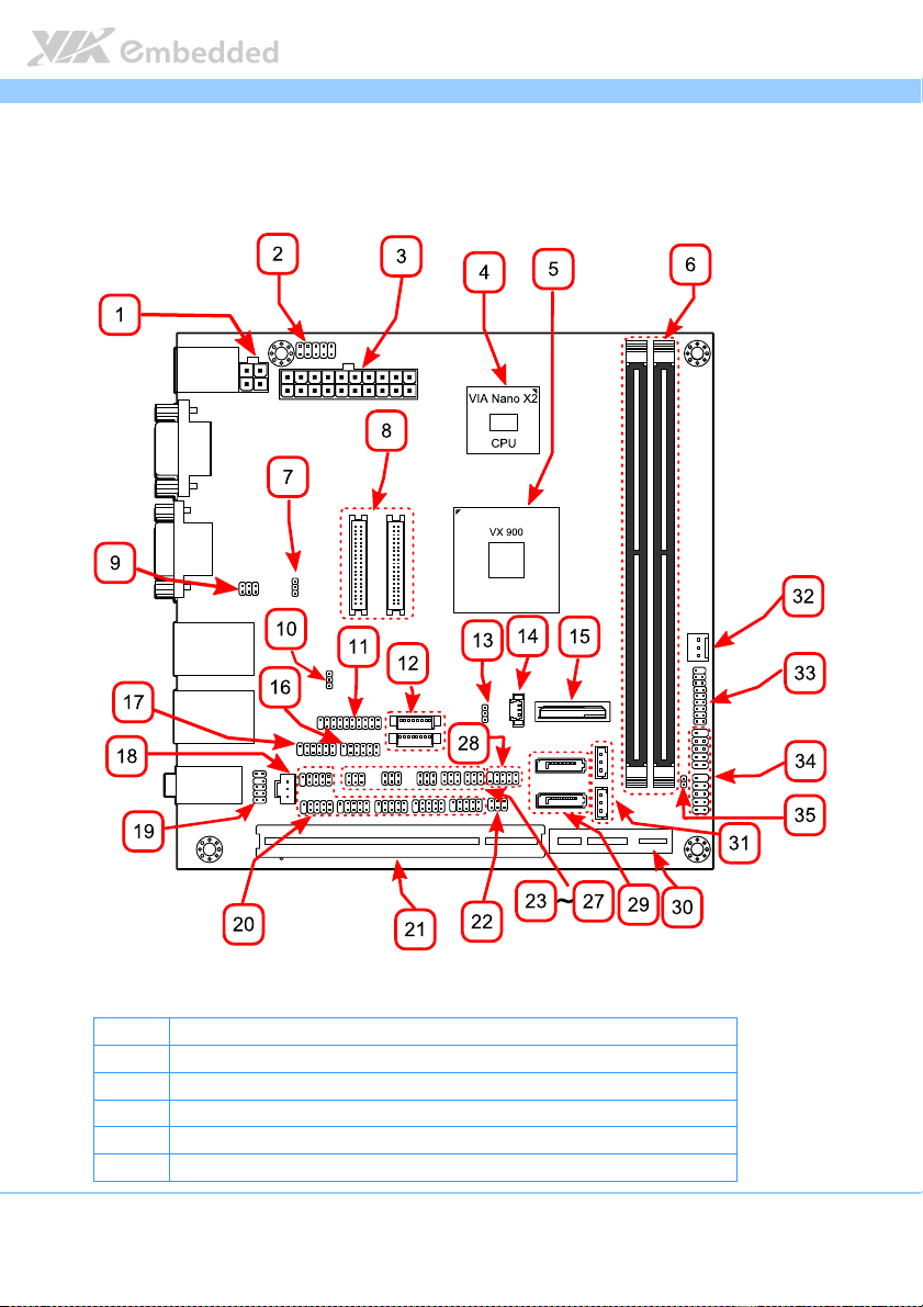
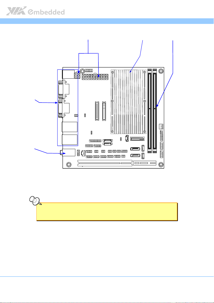
1.3. Layout Diagram
M910 User Manual
User Manual
M910 M910
User ManualUser Manual
Figure
Figure 1111: Layout diagram of the
: Layout diagram of the EPIA
Figure Figure
: Layout diagram of the : Layout diagram of the
Item
Item Description
ItemItem
1 DC-in power connector (DC12V1) * for DC-in SKU only
2 PS/2 keyboard and mouse pin header (KBMS)
3 ATX power supply connector (ATX_POWER1)
4 VIA Nano X2 CPU
5 VIA VX900 chipset
Description
DescriptionDescription
EPIA----MMMM91
910000 mainb
EPIAEPIA
9191
mainboard
oard (top view)
mainb mainb
oardoard
(top view)
(top view) (top view)
7
Page 22

EPIA
6 Memory slots (DIMM1, DIMM2)
7 AT/ATX mode select jumper (J6)
8 LVDS connectors (LVDS1, LVDS2)
9 COM voltage selector jumper for external COM1 and COM2 (J10)
10 SMBus pin header (SMBUS1)
11 LPC pin header (LPC1)
12 LVDS inverter connectors (INVERTER1, INVERTER2)
13 Clear CMOS jumper (CLEAR_CMOS)
14 CPU fan Connector (CPUFAN)
15 CMOS battery socket (BAT1)
16 Digital I/O pin headers (DIO2)
17 Digital I/O pin headers (DIO1)
18 SPDIF connector (SPDIF1)
19 Front audio pin header (F_AUDIO1)
20 COM pin headers (COM3, COM4, COM5, COM6, COM7, COM8)
21 PCI slot (PCI_SLOT)
22 SATA DOM power select jumper (J1)
23 COM voltage selector jumper for COM5 and COM6 (J14)
24 COM voltage selector jumper for COM7 and COM8 (J15)
25 COM voltage selector jumper for COM3 and COM4 (J13)
26 LVDS2 power select jumper (J16)
27 LVDS1 power select jumper (J12)
28 SPI pin header
29 SATA connectors (SATA1, SATA2)
30 PCI Express x1 slot (J2)
31 SATA Power (S_PWR1 and S_PWR2) * for DC-in SKU only
32 System fan connector (SYSFAN)
33 Front panel pin header (F_PANEL)
34 USB pin header (USB_1 and USB_2)
35 JATX_ON pin header
EPIA----M910
EPIAEPIA
Note:
For the purposes of simplifying the illustration, the connectors for both DC-in
and ATX Power versions have been included in the diagram. However, actual
products will only have one or the other.
M910 User Manual
User Manual
M910 M910
User ManualUser Manual
8
Page 23
EPIA
EPIA----M910
EPIAEPIA
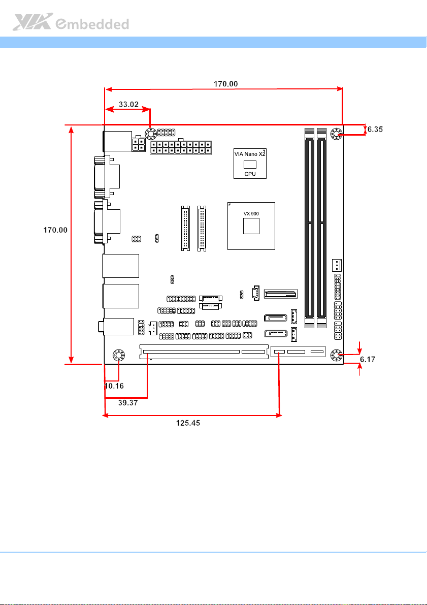
1.4. Product Dimensions
M910 User Manual
User Manual
M910 M910
User ManualUser Manual
Unit: mm
Figure
Figure 2222: Mounting holes and dimensions of the
: Mounting holes and dimensions of the EPIA
Figure Figure
: Mounting holes and dimensions of the : Mounting holes and dimensions of the
EPIA----MMMM91
910000 mainboard
EPIAEPIA
9191
mainboard
mainboard mainboard
9
Page 24
EPIA
Figure
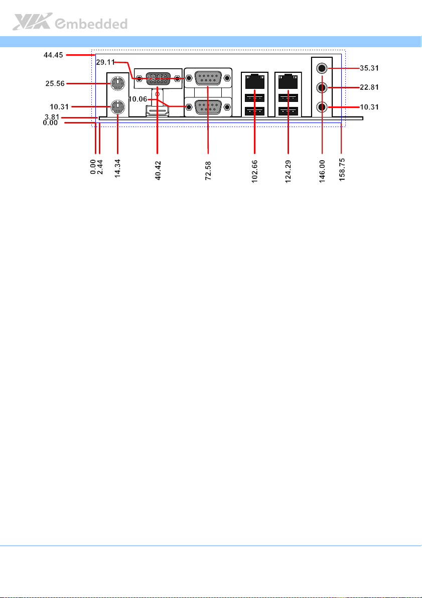
Figure 3333:
: External
External I/O
I/O port
port dimensions of the
Figure Figure
: :
External External
dimensions of the EPIA
I/O I/O
portport
dimensions of the dimensions of the
EPIA----M910
M910 mainboard
EPIAEPIA
M910M910
mainboard
mainboard mainboard
EPIA----M910
EPIAEPIA
M910 User Manual
User Manual
M910 M910
User ManualUser Manual
Unit: mm
10
Page 25
EPIA
Height: 33
Height: 33Height: 33
Height: 33
Height: 3
Height: 3Height: 3
Height: 3
2.4
2.42.4
2.4
Height: 3
Height: 3Height: 3
Height: 3
4.6
4.64.6
4.6
Height: 3
Height: 3Height: 3
Height: 3
2222
Height: 3
Height: 3Height: 3
Height: 3
8.5
8.58.5
8.5
EPIA----M910
EPIAEPIA
1.5. Height Distribution
M910 User Manual
User Manual
M910 M910
User ManualUser Manual
Unit: mm
Figure
Figure 4444: Height distribution of the
: Height distribution of the EPIA
Figure Figure
: Height distribution of the : Height distribution of the
M910
M910----12Q & EPIA
12Q & EPIA----M910
M910M910
12Q & EPIA12Q & EPIA
M910----12PQ)
M910M910
12PQ)
12PQ)12PQ)
EPIA----MMMM91
910000 mainboard
EPIAEPIA
9191
mainboard (for EPIA
mainboard mainboard
(for EPIA----M910
(for EPIA(for EPIA
M910----16, EPIA
16, EPIA----M910
M910M910
16, EPIA16, EPIA
M910----16P, EPIA
16P, EPIA----
M910M910
16P, EPIA16P, EPIA
11
Page 26
EPIA
Height: 33
Height: 33Height: 33
Height: 33
Height: 3
Height: 3Height: 3
Height: 3
5555
Height: 3
Height: 3Height: 3
Height: 3
4.6
4.64.6
4.6
Height: 3
Height: 3Height: 3
Height: 3
2222
Height: 3
Height: 3Height: 3
Height: 3
8.5
8.58.5
8.5
EPIA----M910
EPIAEPIA
Figure
Figure 5555: Height distribution of the EP
: Height distribution of the EPIA
Figure Figure
: Height distribution of the EP: Height distribution of the EP
IA----M910 mainboard
M910 mainboard (for EPIA
IAIA
M910 mainboard M910 mainboard
(for EPIA----M910
(for EPIA(for EPIA
M910----10E & EPIA
10E & EPIA----M910
M910M910
10E & EPIA10E & EPIA
M910 User Manual
User Manual
M910 M910
User ManualUser Manual
M910----10PE)
10PE)
M910M910
10PE)10PE)
Note:
Note:
Note:Note:
All other heights are under 21.00 mm.
12
Page 27
EPIA
2.
2. I/O Interface
I/O Interface
2.2.
I/O InterfaceI/O Interface
The VIA EPIA-M910 has a wide selection of interfaces integrated into the
board. It includes a selection of frequently used ports as part of the external
I/O coastline.
EPIA----M910
M910 User Manual
EPIAEPIA
M910 M910
User Manual
User ManualUser Manual
2.1. External I/O Ports
Figure
Figure 6666: External I/O ports
: External I/O ports
Figure Figure
: External I/O ports: External I/O ports
Item
Item Description
ItemItem
1 PS/2 mouse port
2 VGA port
3 COM ports
4 Gigabit Ethernet ports
5 Line-in 3.5 mm TRS jack
6 Line-out 3.5 mm TRS jack
7 PS/2 keyboard port
8 HDMI port
9 USB 2.0 ports
10 Microphone 3.5 mm TRS jack
Description
DescriptionDescription
13
Page 28

EPIA
12
34
5
6
EPIA----M910
M910 User Manual
EPIAEPIA
M910 M910
User Manual
User ManualUser Manual
2.1.1. PS/2 Port
The mainboard has two integrated PS/2 ports for keyboard and mouse. Each
port is using the 6-pin Mini-DIN connector. The color purple is used for a PS/2
keyboard while the color green is used for a PS/2 mouse. The pinout of the
PS/2 port are shown below.
Pin
Pin
Signal
Signal
PinPin
SignalSignal
1 Data
2 NC
3 Ground
4 +5V
5 Clock
6 NC
Table
Table 1111: PS/2 port pinout
: PS/2 port pinout
Table Table
: PS/2 port pinout: PS/2 port pinout
Figure
Figure 7777:
: PS/2
PS/2 port pinout diagr
Figure Figure
port pinout diagram
: :
PS/2PS/2
port pinout diagr port pinout diagr
am
amam
14
Page 29
EPIA
EPIA----M910
M910 User Manual
EPIAEPIA
M910 M910
User Manual
User ManualUser Manual
2.1.2. VGA Port
The integrated 15-pin VGA port uses a female DE-15 connector. The VGA
port is for connecting to analog displays. The pinout of the VGA port is shown
below.
Figure
Figure 8888: VGA port pinout diagram
: VGA port pinout diagram
Figure Figure
: VGA port pinout diagram: VGA port pinout diagram
Pin
Pin
Signal
Signal
PinPin
SignalSignal
1 RED
2 GREEN
3 BLUE
4 NC
5 Ground
6 Ground
7 Ground
8 Ground
9 +5V
10 NC
11 NC
12 SDA
13 HSync
14 VSync
15 SCL
Table
Table 2222: VGA port pinout
: VGA port pinout
Table Table
: VGA port pinout: VGA port pinout
15
Page 30
EPIA
EPIA----M910
M910 User Manual
EPIAEPIA
M910 M910
User Manual
User ManualUser Manual
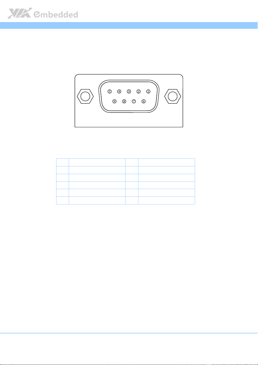
2.1.3. COM Port
The integrated 9-pin COM port uses a male DE-9 connector. The COM
(COM1) port supports the RS-232 standard. The pinout of the COM port is
shown below.
Figure
Figure 9999: COM port pinout diagram
: COM port pinout diagram
Figure Figure
: COM port pinout diagram: COM port pinout diagram
Pin
Pin
Signal
Table
Table 3333:
: COM port pinout
Table Table
: :
Signal Pin
PinPin
SignalSignal
1 DCD 6 DSR
2 RxD 7 RTS
3 TxD 8 CTS
4 DTR 9 RI
5 GND
COM port pinout
COM port pinoutCOM port pinout
Pin
PinPin
Signal
Signal
SignalSignal
16
Page 31

EPIA
EPIA----M910
M910 User Manual
EPIAEPIA
M910 M910
User Manual
User ManualUser Manual
2.1.4. RJ45 LAN port: Gigabit Ethernet
The integrated 8-pin Gigabit Ethernet port is using an 8 Position 8 Contact
(8P8C) receptacle connector (commonly referred to as RJ45). The pinout of
the Gigabit Ethernet port is shown below.
Pin
Pin
Signal
Signal
PinPin
SignalSignal
1 Signal pair 1+
2 Signal pair 1-
3 Signal pair 2+
4 Signal pair 3+
5 Signal pair 3-
6 Signal pair 2-
7 Signal pair 4+
8 Signal pair 4-
Table
Table 4444: Gigabit Ethernet port pinout
: Gigabit Ethernet port pinout
Table Table
: Gigabit Ethernet port pinout: Gigabit Ethernet port pinout
Figure
Figure 10
10: Gigabit Ethernet port pinout diagram
Figure Figure
The RJ-45 port has two individual LED indicators located on the front side to
show its Active/Link status and Speed status.
: Gigabit Ethernet port pinout diagram
1010
: Gigabit Ethernet port pinout diagram: Gigabit Ethernet port pinout diagram
Link LED
(Left LED on RJ
(Left LED on RJ----45 connector)
(Left LED on RJ(Left LED on RJ
Link Off Off Off
Speed_10Mbit The LED is always On in either Green
or Orange colors
Speed_100Mbit The LED is always On in Green color Flash in Yellow color
Speed_1000Mbit The LED is always On in Orange color Flash in Yellow color
Table
Table 5555: Gigabit Ethernet LED color de
: Gigabit Ethernet LED color definition
Table Table
: Gigabit Ethernet LED color de: Gigabit Ethernet LED color de
Link LED
Link LEDLink LED
45 connector)
45 connector)45 connector)
finition
finitionfinition
Active LED
Active LED
Active LEDActive LED
(Right LED on RJ
(Right LED on RJ----45 connector)
(Right LED on RJ(Right LED on RJ
Flash in Yellow color
45 connector)
45 connector)45 connector)
17
Page 32

EPIA
EPIA----M910
M910 User Manual
EPIAEPIA
M910 M910
User Manual
User ManualUser Manual
2.1.5. Audio Ports
There are three audio jack receptacles integrated into a single stack on the I/O
coastline. Each receptacle can fit a 3.5 mm Tip Ring Sleeve (TRS) connector to
enable connections to Line-in, Line-out, and MIC-in.
Wiring
Wiring
WiringWiring
Tip Left channel in Left channel Left channel
Ring Right channel in Right channel Right channel
Sleeve Ground Ground Ground
Table
Table 6666: Audio jack receptacle pino
Table Table
Line
Line----in
in Line
LineLine
inin
: Audio jack receptacle pinout
: Audio jack receptacle pino: Audio jack receptacle pino
Line----out
out MIC
LineLine
outout
ut
utut
MIC----in
MICMIC
in
inin
Figure
Figure 11
Figure Figure
11: Audio jack receptacle stack
1111
: Audio jack receptacle stack
: Audio jack receptacle stack: Audio jack receptacle stack
18
Page 33

EPIA
EPIA----M910
M910 User Manual
EPIAEPIA
M910 M910
User Manual
User ManualUser Manual
2.1.6. HDMI Port
The integrated 19-pin HDMI port uses an HDMI Type A receptacle connector
as defined in the HDMI 1.2 specification. The HDMI (High Definition
Multimedia Interface) port is for connecting the high definition video and
digital audio. It allows you to connect the digital video devices which utilize a
high definition video signal. The pinout of the HDMI port is shown below.
Figure
Figure 12
12: HDMI port pinout diagram
Figure Figure
Table
Table 7777: HDMI port pinout
Table Table
: HDMI port pinout diagram
1212
: HDMI port pinout diagram: HDMI port pinout diagram
Pin
Pin
Signal
Signal Pin
PinPin
SignalSignal
1 TX2+ 2 Ground
3 TX2- 4 TX1+
5 Ground 6 TX1-
7 TX0+ 8 Ground
9 TX0- 10 TXC+
11 Ground 12 TXC-
13 key 14 key
15 DDCSCL 16 DDCSDA
17 Ground 18 +5V
19 Hot Plug Detect
: HDMI port pinout
: HDMI port pinout: HDMI port pinout
Pin
PinPin
Signal
Signal
SignalSignal
19
Page 34

EPIA
EPIA----M910
M910 User Manual
EPIAEPIA
M910 M910
User Manual
User ManualUser Manual
2.1.7. USB 2.0 Port
There are two integrated USB 2.0 ports in EPIA-M910 mainboard. The USB-
interface port gives complete Plug and Play and hot swap capability for
external devices and it complies with USB UHCI, rev. 2.0. Each USB port is
using the USB Type A receptacle connector. The pinout of the typical USB
port is shown below.
Pin
Pin
Signal
Signal
PinPin
SignalSignal
1 +5VSUS
2 Data-
3 Data+
4 Ground
Table
Table 8888: USB port pinout
: USB port pinout
Table Table
: USB port pinout: USB port pinout
Figure
Figure 13
13: USB port pinout diagram
Figure Figure
: USB port pinout diagram
1313
: USB port pinout diagram: USB port pinout diagram
20
Page 35

EPIA
EPIA----M910
M910 User Manual
EPIAEPIA
M910 M910
User Manual
User ManualUser Manual
2.2. Onboard Connectors
2.2.1. ATX Power Connector
The mainboard has a 20-pin ATX power connector onboard. The ATX power
connector is labeled as “ATX_POWER1”. The pinout of the ATX power
connector is shown below.
Figure
Figure 14
14: ATX power conne
Figure Figure
Table
Table 9999: ATX po
Table Table
: ATX power connector
1414
: ATX power conne: ATX power conne
Pin
Pin
PinPin
1 +3.3V 11 +3.3V
2 +3.3V 12 -12V
3 Ground 13 Ground
4 +5V 14 Power Supply On
5 Ground 15 Ground
6 +5V 16 Ground
7 Ground 17 Ground
8 Power OK 18 -5V
9 +5VSB 19 +5V
10 +12V 20 +5V
: ATX power connector pinout
: ATX po: ATX po
wer connector pinout
wer connector pinoutwer connector pinout
21
ctor
ctorctor
Signal
Signal Pin
SignalSignal
Pin
PinPin
Signal
Signal
SignalSignal
Page 36

EPIA
EPIA----M910
M910 User Manual
EPIAEPIA
M910 M910
User Manual
User ManualUser Manual
2.2.2. LVDS panel connectors
The mainboard has two LVDS panel connectors: LVDS1 and LVDS2. LVDS1
connector is controlled by VIA VX900 chipset while the LVDS2 connector is
controlled by VT1636 LVDS transmitter.
Figure
Figure 15
15: LVDS panel connector
Figure Figure
22
: LVDS panel connector
1515
: LVDS panel connector: LVDS panel connector
Pin
Pin
Signal
Signal Pin
PinPin
SignalSignal
M1 GND
2 PVDD1 1 NC
4 PVDD1 3 NC
6 GND 5 GND
8 GND 7 NC
10 -LD1C0 9 NC
12 +LD1C0 11 GND
14 GND 13 NC
16 -LD1C1 15 NC
Pin
PinPin
Signal
Signal
SignalSignal
Page 37

EPIA
18 +LD1C1 17 GND
20 GND 19 NC
22 -LD1C2 21 NC
24 + LD1C2 23 GND
26 GND 25 NC
28 -LCLK1 27 NC
30 + LCLK1 29 NC
32 GND 31 GND
34 -LD1C3 33 NC
36 + LD1C3 35 NC
38 DVP1_SPCLK 37 NC
40 DVP1_SPD 39 NC
Table
Table 10
10: LVDS1
: LVDS1 panel pinout
: LVDS1: LVDS1
panel pinout
panel pinoutpanel pinout
Table Table
1010
EPIA----M910
EPIAEPIA
Pin
Pin
Signal
Table
Table 11
11: LVDS
Table Table
1111
: LVDS2
: LVDS: LVDS
Signal Pin
PinPin
SignalSignal
M1 GND
2 PVDD2 1 -A4_L
4 PVDD2 3 A4_L
6 GND 5 GND
8 GND 7 -A5_L
10 -A0_L 9 A5_L
12 A0_L 11 GND
14 GND 13 -A6_L
16 -A1_L 15 A6_L
18 A1_L 17 GND
20 GND 19 -CLK2_L
22 -A2_L 21 CLK2_L
24 A2_L 23 GND
26 GND 25 -A7_L
28 -CLK1_L 27 A7_L
30 CLK1_L 29 NC
32 GND 31 NC
34 -A3_L 33 NC
36 A3_L 35 NC
38 DISPCLKI0 37 NC
40 DISPCLKO0 39 NC
2 panel pinout
panel pinout
2 2
panel pinoutpanel pinout
Pin
PinPin
Signal
Signal
SignalSignal
M910 User Manual
User Manual
M910 M910
User ManualUser Manual
23
Page 38

EPIA
EPIA----M910
M910 User Manual
EPIAEPIA
M910 M910
User Manual
User ManualUser Manual
2.2.3. LVDS Inverter Connector
The mainboard has two inverters for controlling the LVDS panel backlight and
brightness. INVERTER1 corresponds to the LVDS1 panel connector.
INVERTER2 corresponds to the LVDS2 panel connector.
Figure
Figure 16
16: LVDS Inverter connector
Figure Figure
Table
Table 12
Table Table
24
: LVDS Inverter connector
1616
: LVDS Inverter connector: LVDS Inverter connector
Inverter 1
Inverter 1 Inverter 2
Inverter 1Inverter 1
Pin
Pin
Signal
Signal Pin
PinPin
SignalSignal
1 INV1_12 1 INV2_12
2 INV1_12 2 INV2_12
3 BLON1 3 BLON2
4 VX900PWM_CTL 4 VX900PWM_CTL
5 BLON1 5 BLON2
6 BRIGHTNESS1_CTL 6 BRIGHTNESS2_CTL
7 GND 7 GND
8 GND 8 GND
12:
: LVDS Inverter connector
LVDS Inverter connector pinout
1212
: :
LVDS Inverter connectorLVDS Inverter connector
pinout
pinout pinout
Inverter 2
Inverter 2Inverter 2
Pin Signal
Signal
PinPin
SignalSignal
Page 39

EPIA
EPIA----M910
M910 User Manual
EPIAEPIA
M910 M910
User Manual
User ManualUser Manual
2.2.4. Digital I/O pin headers
The mainboard includes two Digital I/O pin headers that support eight GPO
and eight GPI pins.
Figure
Figure 17
17: Digital I/O pin headers
Figure Figure
Table
Table 13
Table Table
: Digital I/O pin headers
1717
: Digital I/O pin headers: Digital I/O pin headers
DIO
DIO 1111 DIO
DIO DIO
Pin
Pin
Signal
Signal Pin
PinPin
SignalSignal
1 5V_DIO 2 12V_DIO 1 5V_DIO 2 12V_DIO
3 GPO_23 4 GPI_03 3 GPO_27 4 GPI_15
5 GPO_22 6 GPI_02 5 GPO_26 6 GPI_11
7 GPO_21 8 GPI_01 7 GPO_25 8 GPI_10
9 GPO_20 10 GPI_00 9 GPO_24 10 GPI_04
11 GND 12 NC 11 GND 12 NC
13:
: Digital I/O pin headers
Digital I/O pin headers pinout
1313
: :
Digital I/O pin headersDigital I/O pin headers
Pin
Signal
Signal Pin
PinPin
SignalSignal
pinout
pinout pinout
DIO 2222
DIO DIO
Pin
Signal
Signal Signal
PinPin
SignalSignal
Signal
SignalSignal
25
Page 40

EPIA
EPIA----M910
M910 User Manual
EPIAEPIA
M910 M910
User Manual
User ManualUser Manual
2.2.5. DC-in Power Connector
For the DC version of the mainboard, there is a DC-in power connecter in
addition to the DC-in coaxial power connector. This enables two methods for
delivering +12V to the mainboard. The pinout of the DC-in power connector
is shown below.
Figure
Figure 18
18: DC
: DC----in power connector
Figure Figure
Table
Table 14
Table Table
26
in power connector
1818
: DC: DC
in power connectorin power connector
Pin
Pin
Signal
Signal Pin
PinPin
SignalSignal
1 Ground 3 +12V
2 Ground 4 +12V
14: DC
: DC----in power connector pinout
in power connector pinout
1414
: DC: DC
in power connector pinoutin power connector pinout
Note:
Note:
Note:Note:
1. The DC-in version does not have the ATX power connector.
2. The maximum power for DC-in version is 80W.
Pin
PinPin
Si
Signal
gnal
SiSi
gnalgnal
Page 41

EPIA
EPIA----M910
M910 User Manual
EPIAEPIA
M910 M910
User Manual
User ManualUser Manual
2.2.6. SATA Power Connector
For the DC version of the mainboard, there are two built-in SATA power
connectors. These connectors are required to power SATA hard drives. The
SATA power connectors are labeled as “S_PWR1” and “S_PWR2”. The pinout
of the SATA power connectors is shown below.
Figure
Figure 19
19: SATA power connector
Figure Figure
Table
Table 15
Table Table
: SATA power connector
1919
: SATA power connector: SATA power connector
SSSS_PWR
_PWR1111 SSSS_PWR
_PWR_PWR
Pin
Pin
Signal
Signal Pin
PinPin
SignalSignal
1 +5V 1 +5V
2 +12V 2 +12V
3 Ground 3 Ground
15: SATA power connector pinout
: SATA power connector pinout
1515
: SATA power connector pinout: SATA power connector pinout
Note:
Note:
Note:Note:
The ATX version does not have the SATA power connector because power for SATA hard drives is
supplied from the ATX power supply.
_PWR2222
_PWR_PWR
Pin
PinPin
Signal
Signal
SignalSignal
27
Page 42

EPIA
EPIA----M910
M910 User Manual
EPIAEPIA
M910 M910
User Manual
User ManualUser Manual
2.2.7. CMOS Battery Slot
The mainboard is equipped with a CMOS battery slot, which is compatible
with CR2032 coin batteries. The CMOS battery slot is labeled as “BAT2”.
When inserting a CR2032 coin battery, be sure that the positive side is facing
the locking clip.
Figure
Figure 20
20: CMOS battery slot
Figure Figure
: CMOS battery slot
2020
: CMOS battery slot: CMOS battery slot
Pin
Pin
Signal
Signal
PinPin
SignalSignal
1 Ground
2 +3V
Table
Table 16
16: CMOS battery slot pinout
: CMOS battery slot pinout
Table Table
1616
: CMOS battery slot pinout: CMOS battery slot pinout
28
Page 43

EPIA
EPIA----M910
M910 User Manual
EPIAEPIA
M910 M910
User Manual
User ManualUser Manual
2.2.8. Front Panel Pin Header
The front panel pin header consists of 15 pins in a 16-pin block. Pin 15 is
keyed. The front panel pin header is labeled as “F_PANEL1”. It provides access
to system LEDs, power, reset, system speaker and HDD LED. The pinout of the
front panel pin header is shown below.
Figure
Figure 21
21: Front panel pin header
Figure Figure
: Front panel pin header
2121
: Front panel pin header: Front panel pin header
Pin
Pin
Signal
Signal Pin
PinPin
SignalSignal
1 +5VDUAL 2 +5V
3 +5VDUAL 4 HD_LED
5 PWR_LED 6 PWR_BTN
7 +5V 8 Ground
9 NC 10 -RST_SW
11 NC 12 Ground
13 SPEAK 14 NC
15
—
Table
Table 17
17: Front panel pin header pinout
: Front panel pin header pinout
Table Table
1717
: Front panel pin header pinout: Front panel pin header pinout
29
Pin
PinPin
16
Signal
Signal
SignalSignal
NC
Page 44

EPIA
EPIA----M910
M910 User Manual
EPIAEPIA
M910 M910
User Manual
User ManualUser Manual
2.2.9. SMBus Pin Header
The SMBus pin header consists of three pins that allow connecting the SMBus
devices. Devices communicate with a SMBus host and/or other SMBus devices
using the SMBus interface. It is labeled as “SMBUS”. The pinout of the SMBus
pin header is shown below.
Pin
Pin
Signal
Signal
PinPin
SignalSignal
1 SMBCK
2 SMBDT
3 Ground
Table
Table 18
18: SMBus pin header
: SMBus pin header pinout
Table Table
1818
: SMBus pin header: SMBus pin header
pinout
pinout pinout
Figure
Figure 22
Figure Figure
22: SMBus pin header
: SMBus pin header
2222
: SMBus pin header: SMBus pin header
30
Page 45

EPIA
EPIA----M910
M910 User Manual
EPIAEPIA
M910 M910
User Manual
User ManualUser Manual
2.2.10. CPU and System Fan Connectors
There are two fan connectors on board: one for the CPU and one for the
chassis. The fan connector for the CPU is labeled as “CPUFAN1” and the fan
connector for the system is labeled as “SYSFAN1”. The fans provide variable
fan speeds controlled by the BIOS. The pinout of the fan connectors is shown
below.
CPU fan (CPUFAN1)
CPU fan (CPUFAN1)
CPU fan (CPUFAN1)CPU fan (CPUFAN1)
Pin
Pin
Signal
Signal
PinPin
SignalSignal
1 FANI01
2 F_PWM1
3 Ground
System fan (SYSFAN1)
System fan (SYSFAN1)
System fan (SYSFAN1)System fan (SYSFAN1)
Pin
Pin
Signal
Signal
PinPin
SignalSignal
1 FANI02
2 F_PWM2
3 Ground
Table
Table 19
19:
: CPU and System
Table Table
CPU and System Fan connector pinout
1919
: :
CPU and System CPU and System
Fan connector pinoutssss
Fan connector pinoutFan connector pinout
Figure
Figure 23
Figure Figure
23:
: CPU and System
CPU and System Fan connectors
2323
: :
CPU and System CPU and System
Fan connectors
Fan connectorsFan connectors
31
Page 46

EPIA
EPIA----M910
M910 User Manual
EPIAEPIA
M910 M910
User Manual
User ManualUser Manual
2.2.11. SATA Connectors
The two SATA connectors on board can support up to 3 Gb/s transfer speeds.
The SATA connectors are labeled as “SATA1” and “SATA2”. The pinout of the
SATA connectors are shown below.
SATA1
SATA1
SATA1SATA1
Pin
Pin
Signal
Signal
PinPin
SignalSignal
1 Ground
2 STXP_1
3 STXN_1
4 Ground
5 SRXN_1
6 SRXP_1
7 SATA1_+5V
SATA2
SATA2
SATA2SATA2
Pin
Pin
Signal
Signal
PinPin
SignalSignal
1 Ground
2 STXP_2
3 STXN_2
4 Ground
5 SRXN_2
6 SRXP_2
7 SATA2_+5V
Table
Table 20
20: SATA connector pinout
: SATA connector pinoutssss
Table Table
2020
: SATA connector pinout: SATA connector pinout
Figure
Figure 24
24: SATA connectors
Figure Figure
: SATA connectors
2424
: SATA connectors: SATA connectors
Note:
Note:
Note:Note:
If the users want to use the SATA Disk-on-Module flash drive on the board, please use the SATA2 connector.
32
Page 47

EPIA
EPIA----M910
M910 User Manual
EPIAEPIA
M910 M910
User Manual
User ManualUser Manual
2.2.12. USB 2.0 Pin Headers
The mainboard has three USB 2.0 pin header blocks that support up to six USB
2.0 ports. The pin header blocks are labeled as “USB_2”, USB_3, and “USB_4”.
The pinout of the USB pin headers are shown below.
Figure
Figure 25
25: USB pin headers
Figure Figure
: USB pin headers
2525
: USB pin headers: USB pin headers
USB_
USB_1111
USB_USB_
Pin
Pin
Signal
Signal Pin
PinPin
SignalSignal
1 VUSB6 2 VUSB6
3 USBD_T6- 4 USBD_T3-
5 USBD_T6+ 6 USBD_T3+
7 Ground 8 Ground
9
—
Pin
Signal
Signal
PinPin
SignalSignal
10 Ground
USB_
USB_2222
USB_USB_
Pin
Pin
Signal
Signal Pin
PinPin
SignalSignal
1 VUSB2 2 VUSB2
3 USBD_T7- 4 USBD_T2-
5 USBD_T7+ 6 USBD_T2+
7 Ground 8 Ground
9
—
Table
Table 21
21:
: USB pin head
Table Table
USB pin header pinouts
2121
: :
USB pin headUSB pin head
33
Pin
PinPin
10 Ground
er pinouts
er pinoutser pinouts
Signal
Signal
SignalSignal
Page 48

EPIA
EPIA----M910
M910 User Manual
EPIAEPIA
M910 M910
User Manual
User ManualUser Manual
2.2.13. COM Pin Header for COM3~COM8
There are a total of three COM pin headers on the mainboard. Each COM pin
header supports the RS-232 standard. The pin headers are labeled as “COM3”,
“COM4”, “COM5”, “COM6”, “COM7” and “COM8”. All of the COM pin
headers can support +5V or +12V. The pinout of the COM pin headers are
shown below.
Figure
Figure 26
26: COM pin headers
Figure Figure
Table
Table 22
Table Table
34
: COM pin headers
2626
: COM pin headers: COM pin headers
Pin
Pin
Signal
Signal Pin
PinPin
SignalSignal
1 COM_DCDX 2 COM_RXDX
3 COM_TXDX 4 COM_DTRX
5 Ground 6 COM_DSRX
7 COM_RTSX 8 COM_CTSX
9 COM_RIX 10 —
22: COM pin header pinout
: COM pin header pinout
2222
: COM pin header pinout: COM pin header pinout
Pin
PinPin
Signal
Signal
SignalSignal
Page 49

EPIA
EPIA----M910
M910 User Manual
EPIAEPIA
M910 M910
User Manual
User ManualUser Manual
2.2.14. PS/2 Keyboard and Mouse Pin Header
The mainboard has a pin header for a PS/2 keyboard and mouse. The pin
header is labeled as “KBMS1”. The pinout of the pin header is shown below.
Figure
Figure 27
27: PS/2 keyboard and mouse pin header
Figure Figure
: PS/2 keyboard and mouse pin header
2727
: PS/2 keyboard and mouse pin header: PS/2 keyboard and mouse pin header
Pin
Pin
Signal
Signal Pin
PinPin
SignalSignal
1 +5VDUAL 2 Ground
3 KB_CLK 4 KB_DATA
5 EKBCLK 6 EKBDATA
7 MS_CLK 8 MS_DATA
9 EMSCLK 10 EMSDATA
Table
Table 23
23: PS/2 keyboard and mouse pin header
: PS/2 keyboard and mouse pin header pinout
Table Table
2323
: PS/2 keyboard and mouse pin header: PS/2 keyboard and mouse pin header
Note:
Note:
Note:Note:
When the pin header is not in use, please short pin 3&5, pin 4&6, pin 7&9 and pin 8&10
Pin
PinPin
pinout
pinout pinout
Signal
Signal
SignalSignal
35
Page 50

EPIA
EPIA----M910
M910 User Manual
EPIAEPIA
M910 M910
User Manual
User ManualUser Manual
2.2.15. Front Audio Pin Header
In addition to the TRS audio jacks on the external I/O coastline, the mainboard
has a pin header for Line-Out and MIC-In. The pin header is labeled as
“F_AUDIO1”. The pinout of the pin header is shown below.
Figure
Figure 28
28: Front audio pin header
Figure Figure
: Front audio pin header
2828
: Front audio pin header: Front audio pin header
Pin
Pin
Signal
Signal Pin
PinPin
SignalSignal
1 MIC2IN_L 2 AGND
3 MIC2IN_R 4 AGND
5 HPOUTR 6 MIC2_JD
7 F_AUDIO_SENSE 8
9 HPOUTL 10 HPOUT_JD
Table
Table 22224444: Front audio pin header pinout
: Front audio pin header pinout
Table Table
: Front audio pin header pinout: Front audio pin header pinout
36
Pin
PinPin
Signal
Signal
SignalSignal
—
Page 51

EPIA
EPIA----M910
M910 User Manual
EPIAEPIA
M910 M910
User Manual
User ManualUser Manual
2.2.16. SPDIF Connector
The mainboard has one 3-pin SPDIF (Sony Philips Digital Interface) connector.
The SPDIF output provides digital audio to external speakers or compressed
AC3 data to an external Dolby Digital Decoder. The connector is labeled as
“SPDIF1”. The pinout of the connector is shown below.
Figure
Figure 29
29: SPDIF connector
Figure Figure
: SPDIF connector
2929
: SPDIF connector: SPDIF connector
Pin
Pin
Signal
Signal
PinPin
SignalSignal
1 +5V
2 SPDIF_O
3 Ground
Table
Table 25
25: SPDIF conn
: SPDIF connector pinout
Table Table
2525
: SPDIF conn: SPDIF conn
ector pinout
ector pinoutector pinout
37
Page 52

EPIA
EPIA----M910
M910 User Manual
EPIAEPIA
M910 M910
User Manual
User ManualUser Manual
2.2.17. SPI Pin Header
The mainboard has one 8-pin SPI pin header. The SPI (Serial Peripheral
Interface) pin-header is used to connect to the SPI BIOS programming fixture.
The pin header is labeled as “SPI1”. The pinout of the pin header is shown
below.
Figure
Figure 30
30: SPI pin header
Figure Figure
: SPI pin header
3030
: SPI pin header: SPI pin header
Pin
Pin
Signal
Table
Table 26
26: SPI pin header pinout
: SPI pin header pinout
Table Table
2626
: SPI pin header pinout: SPI pin header pinout
Signal Pin
PinPin
SignalSignal
1 SPI_VCC 2 Ground
3 SPI_SS0 4 SPI_CLK
5 SPI_DI 6 SPI_DO
7
—
Pin
Signal
Signal
PinPin
SignalSignal
8 -RST_SW
38
Page 53

EPIA
EPIA----M910
M910 User Manual
EPIAEPIA
M910 M910
User Manual
User ManualUser Manual
2.2.18. LPC Pin Header
The mainboard has one LPC pin header for connecting LPC devices. The pin
header is labeled as “LPC”. The pinout of the pin header is shown below.
Figure
Figure 31
31: LPC pin header
Figure Figure
: LPC pin header
3131
: LPC pin header: LPC pin header
Pin
Pin
Signal
Table
Table 27
27: LPC pin header pinout
: LPC pin header pinout
Table Table
2727
: LPC pin header pinout: LPC pin header pinout
Signal Pin
PinPin
SignalSignal
1 LPC_AD1 2 LPC_33_CLK
3 -PCI_RST-1 4 Ground
5 LPC_AD0 6 NC
7 LPC_AD2 8 -LPC_FRAME
9 SERIRQ 10 LPC_AD3
11 -LPC_DRQ1 12 -EXTSMI
13 +5V 14 +3.3V
15 +5V 16 +3.3V
17 Ground 18 Ground
19 Ground
Pin
PinPin
Signal
Signal
SignalSignal
39
Page 54

EPIA
3.
3. Jumpers
Jumpers
3.3.
JumpersJumpers
EPIA----M910
M910 User Manual
EPIAEPIA
M910 M910
User Manual
User ManualUser Manual
3.1. Clear CMOS Jumper
The onboard CMOS RAM stores system configuration data and has an onboard
battery power supply. To reset the CMOS settings, set the jumper on pins 2
and 3 while the system is off. Return the jumper to pins 1 and 2 afterwards.
Setting the jumper while the system is on will damage the mainboard. The
default setting is on pins 1 and 2.
Figure
Figure 32
32: CLEAR CMOS jumper
Figure Figure
Table
Table 28
Table Table
: CLEAR CMOS jumper
3232
: CLEAR CMOS jumper: CLEAR CMOS jumper
Setting
Setting Pin 1
SettingSetting
Regular (default) On On Off
Clear CMOS Off On On
28: CLEAR CMOS jumper settings
: CLEAR CMOS jumper settings
2828
: CLEAR CMOS jumper settings: CLEAR CMOS jumper settings
Pin 1 Pin 2
Pin 1Pin 1
Pin 2 Pin 3
Pin 2Pin 2
Pin 3
Pin 3Pin 3
40
Page 55

EPIA
EPIA----M910
EPIAEPIA
Note:
Note:
Note:Note:
Except when clearing the RTC RAM, never remove the cap from the CLEAR_CMOS jumper default
position. Removing the cap will cause system boot failure. Avoid clearing the CMOS while the system
is on; it will damage the mainboard.
M910 User Manual
User Manual
M910 M910
User ManualUser Manual
41
Page 56

EPIA
EPIA----M910
M910 User Manual
EPIAEPIA
M910 M910
User Manual
User ManualUser Manual
3.2. SATA DOM Power Select Jumper
The SATA connectors can be used to support Disk-on-Module flash drives.
The power for SATA DOM is controlled by the jumper labeled as “J1”.When
the jumpers are set, +5V will be delivered to the 7
connectors. The jumper settings are shown below.
th
pin of the SATA
Figure
Figure 33
33: SATA DOM voltage select jumper
Figure Figure
Table
Table 29
Table Table
: SATA DOM voltage select jumper
3333
: SATA DOM voltage select jumper: SATA DOM voltage select jumper
SATA1
SATA1 Setting
Setting Pin 2
SATA1SATA1
Setting Setting
DOM support On On Off
Regular (default) Off On On
SATA2 Setting
SATA2 Setting Pin 1
SATA2 SettingSATA2 Setting
DOM support On On Off
Regular (default) Off On On
29: SATA DOM voltage select jumper settings
: SATA DOM voltage select jumper settings
2929
: SATA DOM voltage select jumper settings: SATA DOM voltage select jumper settings
Pin 2 Pin 4
Pin 2Pin 2
Pin 1 Pin 3
Pin 1Pin 1
Pin 4 Pin 6
Pin 4Pin 4
Pin 3 Pin 5
Pin 3Pin 3
Pin 6
Pin 6Pin 6
Pin 5
Pin 5Pin 5
42
Page 57

EPIA
EPIA----M910
M910 User Manual
EPIAEPIA
M910 M910
User Manual
User ManualUser Manual
3.3. COM1 and COM2 Voltage Select Jumper
The voltage for COM1 and COM2 is controlled by the jumper labeled as
“J10”. The voltage can be either +5V or +12V. +5V is the default setting. The
odd pin numbers correspond to COM1. The even pin numbers correspond to
COM2. The jumper settings are shown below.
Figure
Figure 34
34: COM
: COM1111 and
and COM
COM2222 voltage select jumper
Figure Figure
3434
Table
Table 30
30: COM
Table Table
3030
: COM: COM
and and
: COM1 and
1 and COM
: COM: COM
1 and 1 and
voltage select jumper
COMCOM
voltage select jumper voltage select jumper
COM1 Setting
COM1 Setting Pin 1
COM1 SettingCOM1 Setting
+5V (default) On On Off
+12V Off On On
COM2 Setting
COM2 Setting Pin 2
COM2 SettingCOM2 Setting
+5V (default) On On Off
+12V Off On On
COM2222 voltage select jumper settings
voltage select jumper settings
COMCOM
voltage select jumper settings voltage select jumper settings
Pin 1 Pin 3
Pin 1Pin 1
Pin 2 Pin 4
Pin 2Pin 2
Pin 3 Pin 5
Pin 3Pin 3
Pin 4 Pin 6
Pin 4Pin 4
Pin 5
Pin 5Pin 5
Pin 6
Pin 6Pin 6
43
Page 58

EPIA
EPIA----M910
M910 User Manual
EPIAEPIA
M910 M910
User Manual
User ManualUser Manual
3.4. COM3 and COM4 Voltage Select Jumper
The voltage for COM3 and COM4 is controlled by the jumper labeled as
“J13”. The voltage can be either +5V or +12V. +5V is the default setting. The
odd pin numbers correspond to COM3. The even pin numbers correspond to
COM4. The jumper settings are shown below.
Figure
Figure 35
35: COM
: COM3333 and COM
Figure Figure
3535
Table
Table 31
31: COM
Table Table
3131
and COM4444 vo
: COM: COM
and COM and COM
: COM3333 and COM
and COM4444 voltage select jumper settings
: COM: COM
and COM and COM
voltage select jumper
ltage select jumper
vo vo
ltage select jumperltage select jumper
COM
COM3333 Setting
Setting Pin 2
COMCOM
Setting Setting
+5V (default) On On Off
+12V Off On On
COM
COM4444 Setting
Setting Pin 1
COMCOM
Setting Setting
+5V (default) On On Off
+12V Off On On
voltage select jumper settings
voltage select jumper settings voltage select jumper settings
Pin 2 Pin 4
Pin 2Pin 2
Pin 1 Pin 3
Pin 1Pin 1
Pin 4 Pin 6
Pin 4Pin 4
Pin 3 Pin 5
Pin 3Pin 3
Pin 6
Pin 6Pin 6
Pin 5
Pin 5Pin 5
44
Page 59

EPIA
EPIA----M910
M910 User Manual
EPIAEPIA
M910 M910
User Manual
User ManualUser Manual
3.5. COM5 and COM6 Voltage Select Jumper
The voltage for COM5 and COM6 is controlled by the jumper labeled as
“J14”. The voltage can be either +5V or +12V. +5V is the default setting. The
odd pin numbers correspond to COM5. The even pin numbers correspond to
COM6. The jumper settings are shown below.
Figure
Figure 36
36: COM5 and COM6 voltage select jumper
Figure Figure
Table
Table 32
Table Table
: COM5 and COM6 voltage select jumper
3636
: COM5 and COM6 voltage select jumper: COM5 and COM6 voltage select jumper
COM
COM5
5 Setting
Setting Pin 2
COMCOM
5 5
SettingSetting
+5V (default) On On Off
+12V Off On On
COM
COM6666 Setting
Setting Pin 1
COMCOM
Setting Setting
+5V (default) On On Off
+12V Off On On
32: COM5 and COM6 voltage select jumper settings
: COM5 and COM6 voltage select jumper settings
3232
: COM5 and COM6 voltage select jumper settings: COM5 and COM6 voltage select jumper settings
Pin 2 Pin 4
Pin 2Pin 2
Pin 1 Pin 3
Pin 1Pin 1
Pin 4 Pin 6
Pin 4Pin 4
Pin 3 Pin 5
Pin 3Pin 3
Pin 6
Pin 6Pin 6
Pin 5
Pin 5Pin 5
45
Page 60

EPIA
EPIA----M910
M910 User Manual
EPIAEPIA
M910 M910
User Manual
User ManualUser Manual
3.6. COM7 and COM8 Voltage Select Jumper
The voltage for COM7 and COM8 is controlled by the jumper labeled as
“J15”. The voltage can be either +5V or +12V. +5V is the default setting. The
odd pin numbers correspond to COM7. The even pin numbers correspond to
COM8. The jumper settings are shown below.
Figure
Figure 37
37: COM
: COM7777 and COM
Figure Figure
3737
Table
Table 33
33: COM
Table Table
3333
and COM8888 voltage select jumper
: COM: COM
and COM and COM
: COM7777 and COM
and COM8888 voltage select jumper settings
: COM: COM
and COM and COM
voltage select jumper
voltage select jumper voltage select jumper
COM
COM7777 Setting
Setting Pin 2
COMCOM
Setting Setting
+5V (default) On On Off
+12V Off On On
COM8 Setting
COM8 Setting Pin 1
COM8 SettingCOM8 Setting
+5V (default) On On Off
+12V Off On On
voltage select jumper settings
voltage select jumper settings voltage select jumper settings
Pin 2 Pin 4
Pin 2Pin 2
Pin 1 Pin 3
Pin 1Pin 1
Pin 4 Pin 6
Pin 4Pin 4
Pin 3 Pin 5
Pin 3Pin 3
Pin 6
Pin 6Pin 6
Pin 5
Pin 5Pin 5
46
Page 61

EPIA
EPIA----M910
M910 User Manual
EPIAEPIA
M910 M910
User Manual
User ManualUser Manual
3.7. LVDS Jumper Settings
The LVDS connectors and LVDS inverters can operate on different input
voltages. The mainboard has one jumper (J12) that controls the voltage
delivered to the LVDS1 panel connector and input voltage delivered to the
INVERTER1 connector. The mainboard has one jumper (J16) that controls the
voltage delivered to the LVDS2 panel connector and input voltage delivered
to the INVERTER2 connector.
Figure
Figure 38
38: LVDS jumper
Figure Figure
LVDS1 (J12) LVDS2 (J16)
: LVDS jumper settings
3838
: LVDS jumper: LVDS jumper
Inverter1
Inverter1 power
Inverter1 Inverter1
+12V (default) On On Off
+5V Off On On
LVDS1
LVDS1 power
LVDS1 LVDS1
+3.3V (default) On On Off
+5V Off On On
power
powerpower
power Pin 2
powerpower
settings
settings settings
Pin
Pin 1111 Pin
Pin Pin
Pin 2 Pin 4
Pin 2Pin 2
Pin 3333 Pin
Pin Pin
Pin 4 Pin 6
Pin 4Pin 4
Pin 5555
Pin Pin
Pin 6
Pin 6Pin 6
Inverter2
Inverter2 power
Inverter2 Inverter2
+12V (default) On On Off
+5V Off On On
LVDS2
LVDS2 power
LVDS2 LVDS2
+3.3V (default) On On Off
+5V Off On On
power
powerpower
power Pin 2
powerpower
Pin
Pin 1111 Pin
Pin Pin
Pin 2 Pin 4
Pin 2Pin 2
Pin 3333 Pin
Pin Pin
Pin 4 Pin 6
Pin 4Pin 4
Pin 5555
Pin Pin
Pin 6
Pin 6Pin 6
Table
Table 34
34:
: LVDS
LVDS jumper
jumper settings
Table Table
3434
: :
LVDS LVDS
47
jumper jumper
settings
settingssettings
Page 62

EPIA
EPIA----M910
M910 User Manual
EPIAEPIA
M910 M910
User Manual
User ManualUser Manual
3.8. AT/ATX Mode Jumper (1-2: ATX/2-3:AT)
The AT/ATX jumper enables the user to specify AT or ATX power mode
support. To enable support for +3.3V, the jumper must be set to ATX mode.
Figure
Figure 39
39:
: AT/ATX mode jumper
Figure Figure
AT/ATX mode jumper
3939
: :
AT/ATX mode jumperAT/ATX mode jumper
Setting
Setting 1111 2222 3333
SettingSetting
ATX mode (Default) On On Off
AT mode Off On On
Table
Table 35
35:
: AT/ATX mode jumper
Table Table
AT/ATX mode jumper
3535
: :
AT/ATX mode jumperAT/ATX mode jumper
48
Page 63

EPIA
EPIA----M910
M910 User Manual
EPIAEPIA
M910 M910
User Manual
User ManualUser Manual
3.9. JATX_on Mode Jumper
The JATX_on jumper enables the user to boot AT mode without battery.
Figure
Figure 40
40: JATX_on
Figure Figure
: JATX_on mode jumper
4040
: JATX_on : JATX_on
mode jumper
mode jumpermode jumper
Setting
Setting 1111 2222
SettingSetting
AT mode On On
Normal Off Off
Table
Table 36
36: JATX_on
: JATX_on mode jumper
Table Table
3636
: JATX_on : JATX_on
mode jumper
mode jumpermode jumper
49
Page 64

Page 65

EPIA
4.
4. Expansion Slots
Expansion Slots
4.4.
Expansion SlotsExpansion Slots
EPIA----M910
M910 User Manual
EPIAEPIA
M910 M910
User Manual
User ManualUser Manual
4.1. DDR3 Memory Slots
The mainboard provide one DDR3 DIMM memory slot. The memory slot can
accommodate up to 4 GB of 1066 MHz memory. The memory slot is labeled
as “DIMM1”. The location of the DDR3 memory slot is shown below.
Figure
Figure 41
41: DDR3 memory slot
Figure Figure
51
: DDR3 memory slotssss
4141
: DDR3 memory slot: DDR3 memory slot
Page 66

EPIA
EPIA----M910
M910 User Manual
EPIAEPIA
M910 M910
User Manual
User ManualUser Manual
4.1.1. Installing a Memory Module
Step 1
Step 1
Step 1Step 1
Disengage the locking mechanism at both ends of the DIMM slot by pressing
the retaining clips outward.
Figure
Figure 42
42: Unlocking the memory DIMM slot
Figure Figure
Step
Step 2222
Step Step
Align the notch on the DIMM memory module with the counter part on the
DIMM slot.
: Unlocking the memory DIMM slot
4242
: Unlocking the memory DIMM slot: Unlocking the memory DIMM slot
Figure
Figure 43
43: I
: Inserting the
Figure Figure
nserting the memory
4343
: I: I
nserting thenserting the
memory module
memory memory
module
modulemodule
52
Page 67

EPIA
Step
Step 3333
Step Step
EPIA----M910
M910 User Manual
EPIAEPIA
M910 M910
User Manual
User ManualUser Manual
Insert the DIMM memory module into the slot and push down at both ends
until the locking clips lock the DIMM memory module into place.
Fig
Figure
ure 44
44:
: Locking the memory module
FigFig
Locking the memory module
ure ure
4444
: :
Locking the memory moduleLocking the memory module
53
Page 68

EPIA
EPIA----M910
M910 User Manual
EPIAEPIA
M910 M910
User Manual
User ManualUser Manual
4.1.2. Removing a Memory Module
Step 1
Step 1
Step 1Step 1
To disengage the locking clips, push outward the locking clips on both ends
of memory slot. When the locking clips have cleared, the DIMM memory
module will automatically pop up. Remove the memory module.
Figure
Figure 45
45:
: Removing the memory module
Figure Figure
Removing the memory module
4545
: :
Removing the memory moduleRemoving the memory module
54
Page 69

EPIA
EPIA----M910
M910 User Manual
EPIAEPIA
M910 M910
User Manual
User ManualUser Manual
4.1.3. PCI Slot
The onboard PCI slot, labeled as “PCI_SLOT1”, supports 5V 32-bit PCI cards. It
is not compatible with PCI cards requiring 3.3V signaling. The location of the
PCI slot is shown below.
Figure
Figure 46
46: PCI slot
Figure Figure
: PCI slot
4646
: PCI slot: PCI slot
Note:
1. The orientation of PCI card can be changed from vertical to horizontal using a riser card module.
2. When adding or removing expansion card, unplug first the power supply.
55
Page 70

EPIA
EPIA----M910
M910 User Manual
EPIAEPIA
M910 M910
User Manual
User ManualUser Manual
4.1.4. PCI Express Slot
The onboard PCI Express slot is located adjacent to the PCI slot. The PCI
Express slot provides support for 1-lane cards. Due to the orientation of the
1
slot, a riser card module
shown below.
must be used. The location of the PCI Express slot is
Figure
Figure 47
47: PCI Express slot
Figure Figure
: PCI Express slot
4747
: PCI Express slot: PCI Express slot
Note:
Note:
Note:Note:
1. The optional riser card module is PCIE-03. PCIE-03 is a combination riser card that connects to both
the PCI Express and PCI slots.
56
Page 71

EPIA
5.
5. Hardware Installation
Hardware Installation
5.5.
Hardware InstallationHardware Installation
EPIA----M910
M910 User Manual
EPIAEPIA
M910 M910
User Manual
User ManualUser Manual
5.1. Installing into a Chassis
The EPIA-M910 can be fitted into any chassis that has the mounting holes for
compatible with the standard Mini-ITX mounting hole locations. Additionally,
the chassis must meet the minimum height requirements for specified areas of
the mainboard. If a riser card module is being used, the chassis will need to
accommodate the additional space requirements.
5.1.1. Suggested minimum chassis dimensions
The figure below shows the suggested minimum space requirements that a
chassis should have in order to work well with the EPIA-M910.
Figure
Figure 48
48: Suggested minimum chassis dimensions
Figure Figure
: Suggested minimum chassis dimensions
4848
: Suggested minimum chassis dimensions: Suggested minimum chassis dimensions
57
Page 72

EPIA
EPIA----M910
M910 User Manual
EPIAEPIA
M910 M910
User Manual
User ManualUser Manual
Each side of the mainboard should have a buffer zone from the internal wall
of the chassis. The side of the mainboard that accommodates the I/O coastline
should have a buffer of 1.00 mm. The side on the opposite end of the I/O
coastline should have a buffer of at least 5.00 mm. The two sides adjacent to
the I/O coastline should have at least a 10.00 mm buffer.
For the side that is close to the PCI slot, the buffer should be at least 100.00
mm if a riser card module will be used.
5.1.2. Suggested minimum chassis height
The figure below shows the suggested minimum height requirements for the
internal space of the chassis. It is not necessary for the internal ceiling to be
evenly flat. What is required is that the internal ceiling height must be strictly
observed for each section that is highlighted. The highest part of the ceiling
will be above the PCI slot.
Figure
Figure 49
49: Sugge
: Suggested minimum internal chassis ceiling height
Figure Figure
4949
sted minimum internal chassis ceiling height
: Sugge: Sugge
sted minimum internal chassis ceiling heightsted minimum internal chassis ceiling height
58
Page 73

EPIA
EPIA----M910
M910 User Manual
EPIAEPIA
M910 M910
User Manual
User ManualUser Manual
5.1.3. Suggested keepout areas
The figure below shows the areas of the mainboard that is highly suggested to
leave unobstructed.
Figure
Figure 50
50: Suggested keepout areas
Figure Figure
: Suggested keepout areas
5050
: Suggested keepout areas: Suggested keepout areas
59
Page 74

Page 75

EPIA
6.
6. BIOS Setup Utility
BIOS Setup Utility
6.6.
BIOS Setup UtilityBIOS Setup Utility
EPIA----M910
EPIAEPIA
6.1. Entering the BIOS Setup Utility
M910 User Manual
User Manual
M910 M910
User ManualUser Manual
Power on the computer and press Delete
sequence to enter the BIOS Setup Utility. If the entry point has passed, restart
the system and try again.
Delete during the beginning of the boot
DeleteDelete
6.2. Control Keys
Up
Up Move up one row
UpUp
Down
Down Move down one row
DownDown
Left
Left Move to the left in the navigation bar
LeftLeft
Right
Right Move to the right in the navigation bar
RightRight
Enter
Enter Access the highlighted item / Select the item
EnterEnter
Esc
Esc Jumps to the Exit screen or returns to the previous screen
EscEsc
Page up /
Page up / ++++1 Increase the numeric value
Page up / Page up /
1
Pa
Page down /
ge down / ----
PaPa
ge down / ge down /
F1
F1 General help
F1F1
FFFF5555 Restore the previous CMOS value
FFFF7777 Load optimized defaults
Decrease the numeric value
2
F10
F10 Save all the changes and exit
F10F10
Note:
Note:
Note:Note:
1. Must be pressed using the 10-key pad.
2. The General help contents are only for the Status Page and Option Page setup menus.
61
Page 76

EPIA
EPIA----M910
EPIAEPIA
6.3. Navigating the BIOS Menus
M910 User Manual
User Manual
M910 M910
User ManualUser Manual
The main menu displays all the BIOS setup categories. Use the <Left
and <Up
Up>/<Down
Down> arrow keys to select any item or sub-menu. Descriptions
UpUp
DownDown
of the selected/highlighted category are displayed at the bottom of the screen.
The small triangular arrowhead symbol next to a field indicates that a sub-
menu is available (see figure below). Press <Enter
To exit the sub-menu, press <Esc
Esc>.
EscEsc
Enter> to display the sub-menu.
EnterEnter
Left>/<Right
LeftLeft
Right>
RightRight
6.4. Getting Help
The BIOS Setup Utility provides a “General Help
accessed at any time by pressing F1
using and navigating the BIOS Setup Utility. Press Esc
General Help” screen. This screen can be
General HelpGeneral Help
F1. The help screen displays the keys for
F1F1
Esc to exit the help screen.
EscEsc
62
Page 77

EPIA
EPIA----M910
M910 User Manual
EPIAEPIA
M910 M910
User Manual
User ManualUser Manual
6.5. Main Menu
The System Overview screen is the default screen that is shown when the
BIOS Setup Utility is launched. This screen can be accessed by traversing the
navigation bar to the “Main” label.
Figure
Figure 51
51: Illustration of the Main menu screen
Figure Figure
: Illustration of the Main menu screen
5151
: Illustration of the Main menu screen: Illustration of the Main menu screen
6.5.1. AMIBIOS
The content in this section of the screen shows the current BIOS version, build
date, and ID number.
6.5.2. Processor
This content in this section shows the CPU information that has been detected.
This information includes the CPU name and speed
6.5.3. System Memory
This section shows the amount of available memory that has been detected.
63
Page 78

EPIA
EPIA----M910
M910 User Manual
EPIAEPIA
M910 M910
User Manual
User ManualUser Manual
6.5.4. System Time
This section shows the current system time. Press Tab
Shift+Tab
Shift+Tab to traverse left through the hour, minute, and second segments. The
Shift+TabShift+Tab
++++ and ---- keys on the number pad can be used to change the values. The time
format is [Hour : Minute : Second].
Tab to traverse right and
TabTab
6.5.5. System Date
This section shows the current system date. Press Tab
Shift+Tab
Shift+Tab to traverse left through the month, day, and year segments. The ++++
Shift+TabShift+Tab
and ---- keys on the number pad can be used to change the values. The weekday
name is automatically updated when the date is altered. The date format is
[Weekday, Month, Day, Year].
Tab to traverse right and
TabTab
64
Page 79

EPIA
EPIA----M910
M910 User Manual
EPIAEPIA
M910 M910
User Manual
User ManualUser Manual
6.6. Advanced Settings
The Advanced Settings screen shows a list of categories that can provide
access to a sub-screen. Sub-screen links can be identified by the preceding
right-facing arrowhead.
Figure
Figure 52
52: Illustration of the Advanced Settings screen
Figure Figure
: Illustration of the Advanced Settings screen
5252
: Illustration of the Advanced Settings screen: Illustration of the Advanced Settings screen
The Advanced Settings screen contains the following links:
CPU Configuration
IDE Configuration
SuperIO Configuration
Hardware Health Configuration
ACPI Configuration
APM Configuration
Spread Spectrum Configuration
USB Configuration
CRB Configuration
65
Page 80

EPIA
EPIA----M910
M910 User Manual
EPIAEPIA
M910 M910
User Manual
User ManualUser Manual
6.6.1. CPU Configuration
The CPU Configuration screen shows detailed information about the built-in
processor. In addition to the processor information, the thermal controls can
be set.
Figure
Figure 53
53: Illustration of the CPU Configuration screen
Figure Figure
: Illustration of the CPU Configuration screen
5353
: Illustration of the CPU Configuration screen: Illustration of the CPU Configuration screen
6.6.1.1.
6.6.1.1. PMON
6.6.1.1.6.6.1.1.
PMON
PMONPMON
The Nano CPU PMON Function has two settings: “Auto” and “Disabled”. When
set to “Auto”, the PMON function will be enabled and controlled the CPU
speed to perform automatically at best performance to comply with the given
system applications.
66
Page 81

EPIA
EPIA----M910
M910 User Manual
EPIAEPIA
M910 M910
User Manual
User ManualUser Manual
6.6.2. IDE Configuration
The IDE Configuration screen shows links to the primary master and slave IDE
hard drive information screens.
Figure
Figure 54
54: Illustration of SATA Configuration screen
Figure Figure
: Illustration of SATA Configuration screen
5454
: Illustration of SATA Configuration screen : Illustration of SATA Configuration screen
67
Page 82

EPIA
EPIA----M910
M910 User Manual
EPIAEPIA
M910 M910
User Manual
User ManualUser Manual
6.6.3. SuperIO Configuration
The SuperIO Configuration screen shows the specific addresses and IRQs of
the onboard serial ports.
Figure
Figure 55
55: Illustration of SuperIO Configuration screen
Figure Figure
6.6.3.1.
6.6.3.1. Serial Ports 1 to 8 Address
6.6.3.1.6.6.3.1.
The Serial Port 1 to 2 has three selectable options.
: Illustration of SuperIO Configuration screen
5555
: Illustration of SuperIO Configuration screen: Illustration of SuperIO Configuration screen
Serial Ports 1 to 8 Address
Serial Ports 1 to 8 AddressSerial Ports 1 to 8 Address
Port
Table
Table 37
37: Serial port addresses and IRQs
: Serial port addresses and IRQs
Table Table
3737
: Serial port addresses and IRQs: Serial port addresses and IRQs
Port Address and IRQs
PortPort
1 280/IRQ3
2 288/IRQ3
3
4
5
6
7
8
Address and IRQs
Address and IRQsAddress and IRQs
3F8/IRQ4
2F8/IRQ4
3E8/IRQ4
2E8/IRQ4
2B0/IRQ4
2B8/IRQ4
68
Page 83

EPIA
EPIA----M910
M910 User Manual
EPIAEPIA
M910 M910
User Manual
User ManualUser Manual
6.6.4. Hardware Health Configuration
The Hardware Health Configuration screen has no editable fields. The system
temperature is taken from an optional sensor that is connected to the J5 pin
header.
Figure
Figure 56
56: Illustration of Hardware Health Configuration screen
Figure Figure
: Illustration of Hardware Health Configuration screen
5656
: Illustration of Hardware Health Configuration screen: Illustration of Hardware Health Configuration screen
6.6.4.1.
6.6.4.1. CPU
6.6.4.1.6.6.4.1.
The CPU/System FAN has two selectable mode options.
Auto
Auto
AutoAuto
When set to Auto, the speed of the CPU fan is varied according to CPU
temperature.
Full Speed
Full Speed
Full SpeedFull Speed
When set to Full Speed, the CPU fan speed is fixed and running at highest
speed.
CPU/System
/System Fan Mode Setting
CPUCPU
/System/System
Fan Mode Setting
Fan Mode SettingFan Mode Setting
69
Page 84

EPIA
EPIA----M910
M910 User Manual
EPIAEPIA
M910 M910
User Manual
User ManualUser Manual
6.6.5. ACPI Settings
ACPI grants the operating system direct control over system power
management. The ACPI Configuration screen can be used to set a number of
power management related functions.
Figure
Figure 57
57: Illustration of ACPI Configuration screen
Figure Figure
: Illustration of ACPI Configuration screen
5757
: Illustration of ACPI Configuration screen: Illustration of ACPI Configuration screen
6.6.5.1.
6.6.5.1. Suspend Mode
6.6.5.1.6.6.5.1.
Suspend Mode
Suspend ModeSuspend Mode
The Suspend Mode field has three selectable options.
S1
S1 (POS)
(POS)
S1S1
(POS)(POS)
S1/Power On Suspend (POS) is a low power state. In this state, no system
context (CPU or chipset) is lost and hardware maintains all system contexts.
S3
S3 (STR)
(STR)
S3S3
(STR)(STR)
S3/Suspend To RAM (STR) is a power-down state. In this state, power is
supplied only to essential components such as main memory and wakeup-
capable devices. The system context is saved to main memory, and context is
restored from the memory when a "wakeup" event occurs.
70
Page 85

EPIA
Auto
Auto
AutoAuto
When the Suspend Mode is set to Auto, the operating system will control the
power state.
6.6.5.2.
6.6.5.2. ACPI Version Features
6.6.5.2.6.6.5.2.
The ACPI Version has three selectable version options.
ACPI v1.0
ACPI v1.0
ACPI v1.0ACPI v1.0
Supports ACPI v1.0
ACPI v2.0
ACPI v2.0
ACPI v2.0ACPI v2.0
Supports ACPI v2.0
ACPI v3.0
ACPI v3.0
ACPI v3.0ACPI v3.0
Supports ACPI v3.0
6.6.5.3.
6.6.5.3. USB S4 W
6.6.5.3.6.6.5.3.
The USB S4 WakeUp enables the system to resume through the USB device
port from S4 state. There are two options: “Enabled” or “Disabled”.
ACPI Version Features
ACPI Version FeaturesACPI Version Features
USB S4 Wakeup
USB S4 WUSB S4 W
akeup
akeupakeup
EPIA----M910
M910 User Manual
EPIAEPIA
M910 M910
User Manual
User ManualUser Manual
71
Page 86

EPIA
EPIA----M910
M910 User Manual
EPIAEPIA
M910 M910
User Manual
User ManualUser Manual
6.6.6. APM Settings
APM enables the operating system to co-work with the BIOS to control the
system power management. The APM Configuration screen can be used to set
a number of power management functions.
Figure
Figure 58
58: Illustration of APM Configuration screen
Figure Figure
: Illustration of APM Configuration screen
5858
: Illustration of APM Configuration screen: Illustration of APM Configuration screen
6.6.6.1.
6.6.6.1. Power Button Mode
6.6.6.1.6.6.6.1.
Power Button Mode
Power Button ModePower Button Mode
The Power Button Mode has three options.
On/Off
On/Off
On/OffOn/Off
When On/Off is selected, pressing the power button will instantly cause the
system to power on or off.
Standby
Standby
StandbyStandby
When Standby is selected, the power button must be pressed and held down
for 4 seconds before the system will power off.
Suspend
Suspend
SuspendSuspend
When Suspend is selected, pressing the power button will instantly cause the
system to enter suspend mode.
72
Page 87

EPIA
6.6.6.2.
6.6.6.2. Restore on AC/Power Loss
6.6.6.2.6.6.6.2.
Restore on AC/Power Loss defines how the system will respond after AC
power has been interrupted while the system is on. There are three options.
Power Off
Power Off
Power OffPower Off
The Power Off option keeps the system in an off state until the power button
is pressed again.
Power On
Power On
Power OnPower On
The Power On option restarts the system when the power has returned.
Last State
Last State
Last StateLast State
The Last State option restores the system to its previous state when the power
was interrupted.
6.6.6.3.
6.6.6.3. Resume on PS/2 KBC
6.6.6.3.6.6.6.3.
Resume on PS/2 KBC wakes up a system that has been put into suspend or
standby mode. When this feature is enabled, keyboard activity as defined in
the Wake
three options.
Restore on AC/Power Loss
Restore on AC/Power LossRestore on AC/Power Loss
Resume on PS/2 KBC
Resume on PS/2 KBCResume on PS/2 KBC
Wake----Up Key
Up Key feature will cause the system to wake up. This feature has
WakeWake
Up KeyUp Key
EPIA----M910
M910 User Manual
EPIAEPIA
M910 M910
User Manual
User ManualUser Manual
S3/S4/S5
S3/S4/S5
S3/S4/S5S3/S4/S5
The S3/S4/S5 option enables PS/2 keyboard activity to be detected if the
system is in S3/S4/S5 power saving mode.
Disabled
Disabled
DisabledDisabled
The Disabled option disables the detection of all PS/2 keyboard activity.
6.6.6.4.
6.6.6.4. Wake
6.6.6.4.6.6.6.4.
The Wake-Up Key feature can only be set when Resume on PS/2 KBC
“S3/S4/S5”. Otherwise, this feature will be not selectable. This feature has two
options.
Any Key
Any Key
Any KeyAny Key
The Any Key option enables any key on the keyboard to trigger the Wake-Up
event.
Wake----Up Key
WakeWake
Up Key
Up KeyUp Key
Resume on PS/2 KBC is set to
Resume on PS/2 KBCResume on PS/2 KBC
73
Page 88

EPIA
Specific Key
Specific Key
Specific KeySpecific Key
The Specific Key option unlocks the Wake
6.6.6.5.
6.6.6.5. Wake
6.6.6.5.6.6.6.5.
The Wake-Up Password feature can only be set when the Wake
is set to “Specific Key”. This feature enables the user to specify a key sequence
that must be entered in order to wake up the system.
The key sequence can consist of up to 6 alphanumeric characters and some
special characters. Function keys and modifier keys (such as Ctrl, Alt, Del, etc.)
cannot be used.
6.6.6.6.
6.6.6.6. Resume on PS/2 Mouse
6.6.6.6.6.6.6.6.
Resume on PS/2 Mouse wakes up a system that has been put into suspend or
standby mode. When this feature is enabled, any PS/2 mouse activity that is
detected will cause the system to wake up. This feature has three options.
S3
S3
S3S3
The S3 option enables any PS/2 mouse activity to be detected if the system is
in S3 power saving mode.
Wake----Up Password
WakeWake
Resume on PS/2 Mouse
Resume on PS/2 MouseResume on PS/2 Mouse
Note:
Note:
Note:Note:
This feature supports Erp/Eup provision.
Up Password
Up PasswordUp Password
Wake----Up Password
Up Password feature.
WakeWake
Up PasswordUp Password
EPIA----M910
M910 User Manual
EPIAEPIA
Wake----Up Key
WakeWake
User Manual
M910 M910
User ManualUser Manual
Up Key feature
Up KeyUp Key
S3/S4/S5
S3/S4/S5
S3/S4/S5S3/S4/S5
The S3/S4/S5 option enables any PS/2 mouse activity to be detected if the
system is in S3/S4/S5 power saving mode.
Disabled
Disabled
DisabledDisabled
The Disabled option disables the detection of all PS/2 mouse activity.
6.6.6.7.
6.6.6.7. PCI Lan S5 Wakeup
6.6.6.7.6.6.6.7.
The PCI LAN S5 Wakeup feature enables the BIOS to allow remote wake-up
from the S5 power off state through the PCI bus. This feature has two options:
“Support PCI Lan” and “S5 Wakeup”.
PCI Lan S5 Wakeup
PCI Lan S5 WakeupPCI Lan S5 Wakeup
74
Page 89

EPIA
6.6.6.8.
6.6.6.8. Resume on RTC Alarm
6.6.6.8.6.6.6.8.
Resume on RTC Alarm can only be used if Resume on Software RTC Alarm
not enabled. This feature enables the BIOS to automatically power on the
system at a scheduled time. When enabled, the RTC Alarm Date
Time
Time features will be unlocked.
TimeTime
6.6.6.9.
6.6.6.9. RTC Alarm Date (Days)
6.6.6.9.6.6.6.9.
The RTC Alarm Date feature is visible only when Resume on RTC Alarm
enabled. This feature enables the user to specify a specific date each month or
daily recurrence. Use the ++++ and ---- keys on the number pad to change the value
of the RTC Alarm Date.
Every Day
Every Day
Every DayEvery Day
The Every Day option triggers the RTC Alarm daily.
1
1 –––– 31
31
1 1
31 31
When a specific numeric date is selected, the RTC Alarm will be triggered on
that day of the month.
6.6.6.10.
6.6.6.10. System Time
6.6.6.10.6.6.6.10.
The System Time option enables the user to specify the time the system
should power on for the date that is set in RTC Alarm Date
Resume on RTC Alarm
Resume on RTC AlarmResume on RTC Alarm
RTC Alarm Date (Days)
RTC Alarm Date (Days)RTC Alarm Date (Days)
System Time
System TimeSystem Time
Resume on Software RTC Alarm is
Resume on Software RTC AlarmResume on Software RTC Alarm
RTC Alarm Date and System
RTC Alarm DateRTC Alarm Date
Resume on RTC Alarm is
Resume on RTC AlarmResume on RTC Alarm
RTC Alarm Date.
RTC Alarm DateRTC Alarm Date
EPIA----M910
M910 User Manual
EPIAEPIA
M910 M910
User Manual
User ManualUser Manual
System
System System
75
Page 90

EPIA
EPIA----M910
M910 User Manual
EPIAEPIA
M910 M910
User Manual
User ManualUser Manual
6.6.7. Spread Spectrum Configuration
The Spread Spectrum Configuration screen enables access to the Spread
Spectrum Setting feature.
Figure
Figure 59
59: Illustration of Spread Spectrum Configuration screen
Figure Figure
6.6.7.1.
6.6.7.1. CPU Spread Spectrum Setting
6.6.7.1.6.6.7.1.
The Spread Spectrum Setting feature enables the BIOS to modulate the clock
frequencies originating from the mainboard. The settings are in percentages of
modulation. Higher percentages result in greater modulation of clock
frequencies. This feature has settings that range from 0.1% to 0.9%.
: Illustration of Spread Spectrum Configuration screen
5959
: Illustration of Spread Spectrum Configuration screen: Illustration of Spread Spectrum Configuration screen
CPU Spread Spectrum Setting
CPU Spread Spectrum SettingCPU Spread Spectrum Setting
76
Page 91

EPIA
EPIA----M910
M910 User Manual
EPIAEPIA
M910 M910
User Manual
User ManualUser Manual
6.6.8. USB Configuration
The USB Configuration screen shows the number of connected USB devices.
Figure
Figure 60
60: Illustration of USB Configuration screen
Figure Figure
6.6.8.1.
6.6.8.1. Legacy USB Support
6.6.8.1.6.6.8.1.
The Legacy USB Support feature enables environments that do not have native
USB support to use USB devices. This feature has three options.
: Illustration of USB Configuration screen
6060
: Illustration of USB Configuration screen: Illustration of USB Configuration screen
Legacy USB Support
Legacy USB SupportLegacy USB Support
Auto
Auto
AutoAuto
The Auto option automatically disables legacy support if no USB devices are
connected.
Enabled
Enabled
EnabledEnabled
The Enabled option keeps the Legacy USB Support feature on at all times.
Disabled
Disabled
DisabledDisabled
The Disabled option keeps the Legacy USB Support feature off at all times.
77
Page 92

EPIA
6.6.8.2.
6.6.8.2. USB2.0 Controller Mode
6.6.8.2.6.6.8.2.
The USB 2.0 Controller Mode feature enables the user to set the USB 2.0
controller in HiSpeed (480Mbps) or FullSpeed (12Mbps) mode.
FullSpeed
FullSpeed
FullSpeedFullSpeed
The FullSpeed option limits the USB 2.0 controller to transfer data at 12 Mbps.
HiSpeed
HiSpeed
HiSpeedHiSpeed
The HiSpeed option enables the USB 2.0 controller to transfer data at 480
Mbps. The connected USB device must support USB 2.0 HiSpeed in order to
benefit from this setting.
USB2.0 Controller Mode
USB2.0 Controller ModeUSB2.0 Controller Mode
EPIA----M910
M910 User Manual
EPIAEPIA
M910 M910
User Manual
User ManualUser Manual
78
Page 93

EPIA
EPIA----M910
M910 User Manual
EPIAEPIA
M910 M910
User Manual
User ManualUser Manual
6.6.9. CRB Configuration
The CRB Configuration screen shows the available BIOS-controlled DRAM
clock, graphics adapter, display device and LAN control features.
Figure
Figure 61
61: Illustration of CRB Configuration screen
Figure Figure
6.6.9.1.
6.6.9.1. VT6130 LAN Control
6.6.9.1.6.6.9.1.
The VT6130 LAN Control feature determines whether the onboard LAN
controller will be used or not.
: Illustration of CRB Configuration screen
6161
: Illustration of CRB Configuration screen: Illustration of CRB Configuration screen
VT6130 LAN Control
VT6130 LAN ControlVT6130 LAN Control
6.6.9.2.
6.6.9.2. LAN Option ROM
6.6.9.2.6.6.9.2.
The LAN Option ROM feature will only be visible if the VT6130 LAN Control
feature is enabled. If the LAN Option ROM feature is enabled, then the system
will load a separate ROM for the LAN controller in order to boot from Gigabit
LAN.
LAN Option ROM
LAN Option ROMLAN Option ROM
VT6130 LAN Control
VT6130 LAN ControlVT6130 LAN Control
79
Page 94

EPIA
EPIA----M910
EPIAEPIA
6.7. Boot Settings
M910 User Manual
User Manual
M910 M910
User ManualUser Manual
The Boot Settings screen has a single link that goes to the Boot Settings
Configuration
Configuration and Boot Device Priority
ConfigurationConfiguration
Figure
Figure 62
62: Illustration of Boot Settings screen
Figure Figure
: Illustration of Boot Settings screen
6262
: Illustration of Boot Settings screen: Illustration of Boot Settings screen
Boot Device Priority screens.
Boot Device PriorityBoot Device Priority
Boot Settings
Boot Settings Boot Settings
80
Page 95

EPIA
EPIA----M910
M910 User Manual
EPIAEPIA
M910 M910
User Manual
User ManualUser Manual
6.7.1. Boot Settings Configuration
The Boot Settings Configuration screen has several features that can be run
during the system boot sequence.
Figure
Figure 63
63: Illustration of Boot Settings
Figure Figure
6.7.1.1.
6.7.1.1. Quick Boot
6.7.1.1.6.7.1.1.
The Quick Boot feature enables the BIOS to skip certain tests in order to
speed up the boot sequence. This feature has two options: enabled and
disabled.
: Illustration of Boot Settings Configuration
6363
: Illustration of Boot Settings : Illustration of Boot Settings
Quick Boot
Quick BootQuick Boot
Configuration
ConfigurationConfiguration
6.7.1.2.
6.7.1.2. Quiet Boot
6.7.1.2.6.7.1.2.
The Quiet Boot feature hides all of the Power-on Self Test (POST) messages
during the boot sequence. Instead of the POST messages, the user will see an
OEM logo. This feature has two options: enabled and disabled.
6.7.1.3.
6.7.1.3. Bootup Num
6.7.1.3.6.7.1.3.
The Bootup Num-Lock feature determines how the 10-key pad will behave.
When the feature is enabled, the 10-key pad will behave as a number pad.
When the feature is disabled, the 10-key pad will behave as cursor navigation
keys.
Quiet Boot
Quiet BootQuiet Boot
Bootup Num----Lock
Bootup NumBootup Num
Lock
LockLock
81
Page 96

EPIA
6.7.1.4.
6.7.1.4. Wait for ‘F1’ if Error
6.7.1.4.6.7.1.4.
Wait for ‘F1’ if Error
Wait for ‘F1’ if ErrorWait for ‘F1’ if Error
EPIA----M910
M910 User Manual
EPIAEPIA
M910 M910
User Manual
User ManualUser Manual
This feature determines how the system will respond if an error is detected
during the boot sequence. If this feature is enabled, the BIOS will pause
booting and wait for the user to press F1 to enter the BIOS setup menu. This
feature has two options: enabled and disabled.
6.7.1.5.
6.7.1.5. Hit ‘DEL’ Message Display
6.7.1.5.6.7.1.5.
Hit ‘DEL’ Message Display
Hit ‘DEL’ Message DisplayHit ‘DEL’ Message Display
This feature determines if the BIOS will display a POST message that informs
1
the user how to access the BIOS Setup Utility.
This feature has two options:
enabled and disabled.
Note:
Note:
Note:Note:
If the Quiet Boot option is enabled, the settings of this feature will have no effect.
82
Page 97

EPIA
EPIA----M910
M910 User Manual
EPIAEPIA
M910 M910
User Manual
User ManualUser Manual
6.8. Security Settings
The Security Settings screen provides a way to restrict access to the BIOS or
even the entire system.
Figure
Figure 64
64: Illustration of Security Settings screen
Figure Figure
: Illustration of Security Settings screen
6464
: Illustration of Security Settings screen: Illustration of Security Settings screen
6.8.1. Security Settings
6.8.1.1.
6.8.1.1. Change Supervisor Password
6.8.1.1.6.8.1.1.
This option is for setting a password for accessing the BIOS setup utility.
When a password has been set, a password prompt will be displayed
whenever the BIOS setup utility is launched. This prevents an unauthorized
person from changing any part of the system configuration.
When a supervisor password is set, the Password Check
unlocked.
6.8.1.2.
6.8.1.2. Password Check
6.8.1.2.6.8.1.2.
This feature is compulsory when the Change Supervisor Password
The user will have up to three chances to enter the correct password before
the BIOS forces the system to stop booting. If the user does not enter the
83
Change Supervisor Password
Change Supervisor PasswordChange Supervisor Password
Password Check option will be
Password CheckPassword Check
Password Check
Password CheckPassword Check
Change Supervisor Password option is set.
Change Supervisor PasswordChange Supervisor Password
Page 98

EPIA
EPIA----M910
M910 User Manual
EPIAEPIA
M910 M910
User Manual
User ManualUser Manual
correct password, the keyboard will also lock up. The only way to get past
this is to do a hard reboot (i.e., use the system reset button or cut off the
power to the system). A soft reboot (i.e., Ctrl+Alt+Del) will not work
because the keyboard will be locked. This feature has two options.
Setup
Setup
SetupSetup
The Setup option forces users to enter a password in order to access the BIOS
Setup Utility.
Always
Always
AlwaysAlways
The Always option forces users to enter a password in order to boot up the
system.
84
Page 99

EPIA
EPIA----M910
M910 User Manual
EPIAEPIA
M910 M910
User Manual
User ManualUser Manual
6.9. Advanced Chipset Settings
The Advanced Chipset Settings screen has two links for accessing North and
South bridge functions. Though the VX900 is a single chip solution, the North
and South bridge categories are still for grouping features.
Figure
Figure 65
65: Illustration of Advanced Chipset Settings screen
Figure Figure
: Illustration of Advanced Chipset Settings screen
6565
: Illustration of Advanced Chipset Settings screen: Illustration of Advanced Chipset Settings screen
85
Page 100

EPIA
EPIA----M910
M910 User Manual
EPIAEPIA
M910 M910
User Manual
User ManualUser Manual
6.9.1. North Bridge VIA VX900 Configuration
The North Bridge VIA VX900 Configuration screen contains two links to sub-
screen.
Figure
Figure 66
66: Illustration of North Bridge VIA VX900 Configuration screen
Figure Figure
: Illustration of North Bridge VIA VX900 Configuration screen
6666
: Illustration of North Bridge VIA VX900 Configuration screen: Illustration of North Bridge VIA VX900 Configuration screen
86
 Loading...