

Page 1

USER MANUAL
EPIA-M860
Mini-ITX embedded board
1.14-06212013-165600
Page 2

Copyright
Copyright © 2013 VIA Technologies Incorporated. All rights reserved.
No part of this document may be reproduced, transmitted, transcribed, stored in a retrieval system, or translated into any language,
in any form or by any means, electronic, mechanical, magnetic, optical, chemical, manual or otherwise without the prior written
permission of VIA Technologies, Incorporated.
Trademarks
All trademarks are the property of their respective holders.
Disclaimer
No license is granted, implied or otherwise, under any patent or patent rights of VIA Technologies. VIA Technologies makes no
warranties, implied or otherwise, in regard to this document and to the products described in this document. The information
provided in this document is believed to be accurate and reliable as of the publication date of this document. However, VIA
Technologies assumes no responsibility for the use or misuse of the information (including use or connection of extra
device/equipment/add-on card)
The information and product specifications within this document are subject to change at any time, without notice and without
obligation to notify any person of such change.
VIA Technologies, Inc. reserves the right the make changes to the products described in this manual at any time without prior
notice.
Regulatory Compliance
FCC
FCC----A Radio Frequency Interference Statement
A Radio Frequency Interference Statement
FCCFCC
A Radio Frequency Interference StatementA Radio Frequency Interference Statement
This equipment has been tested and found to comply with the limits for a class A digital device, pursuant to part 15 of the FCC
rules. These limits are designed to provide reasonable protection against harmful interference when the equipment is operated in a
commercial environment. This equipment generates, uses, and can radiate radio frequency energy and, if not installed and used in
accordance with the instruction manual, may cause harmful interference to radio communications. Operation of this equipment in a
residential area is likely to cause harmful interference, in which case the user will be required to correct the interference at his
personal expense.
Notice 1
Notice 1
Notice 1Notice 1
The changes or modifications not expressly approved by the party responsible for compliance could void the user's authority to
operate the equipment.
Notice 2
Notice 2
Notice 2Notice 2
Shielded interface cables and A.C. power cord, if any, must be used in order to comply with the emission limits.
Notice 3
Notice 3
Notice 3Notice 3
The product described in this document is designed for general use, VIA Technologies assumes no responsibility for the conflicts
or damages arising from incompatibility of the product. Check compatibility issue with your local sales representatives before
placing an order.
in this document and for any patent infringements that may arise from the use of this document.
Tested To Comply
With FCC Standards
FOR HOME OR OFFICE USE
Page 3

Battery Recycling and Disposal
Only use the appropriate battery specified for this product.
Do not re-use, recharge, or reheat an old battery.
Do not attempt to force open the battery.
Do not discard used batteries with regular trash.
Discard used batteries according to local regulations.
Safety Precautions
Always read the safety instructions carefully.
Keep this User's Manual for future reference.
All cautions and warnings on the equipment should be noted.
Keep this equipment away from humidity.
Lay this equipment on a reliable flat surface before setting it up.
Make sure the voltage of the power source and adjust properly 110/220V before connecting
the equipment to the power inlet.
Place the power cord in such a way that people cannot step on it.
Always unplug the power cord before inserting any add-on card or module.
If any of the following situations arises, get the equipment checked by authorized service
personnel:
The power cord or plug is damaged.
Liquid has penetrated into the equipment.
The equipment has been exposed to moisture.
The equipment has not worked well or you cannot get it work according to User's Manual.
The equipment has dropped and damaged.
The equipment has obvious sign of breakage.
Do not leave this equipment in an environment unconditioned or in a storage temperature
above 60°C (140°F). The equipment may be damaged.
Do not leave this equipment in direct sunlight.
Never pour any liquid into the opening. Liquid can cause damage or electrical shock.
Do not place anything over the power cord.
Do not cover the ventilation holes. The openings on the enclosure protect the equipment
from overheating
Page 4

EPIA
EPIA----M860
EPIAEPIA
Box Contents and Ordering Information
EPIA
EPIA----M860
M860----12
12EEEE (ATX version)
EPIAEPIA
M860M860
1 x EPIA-M860 embedded board
1 x I/O bracket
1 x SATA cable
EPIA
EPIA----M860
M860----12
EPIAEPIA
M860M860
1 x EPIA-M860 embedded board
1 x I/O bracket
1 x SATA cable
1 x SATA power cable
1 x AC/DC adapter (optional)
(ATX version)
1212
(ATX version) (ATX version)
12PE
PE (DC
(DC----in version)
1212
PEPE
(DC (DC
in version)
in version)in version)
M860 User Manual
User Manual
M860M860
User ManualUser Manual
iv
Page 5

EPIA
EPIA----M860
M860 User Manual
EPIAEPIA
M860M860
Table of Contents
1.1.
Key Features and Benefits........................................................................... 1
1.1.1. VIA Nano™ 1.2GHz Processor............................................................. 1
1.1.2. VIA VX900 Chipset................................................................................. 2
1.1.3. Flexible Power Options ........................................................................ 2
1.1.4. Modular Expansion Options................................................................. 2
1.2.
Product Specifications................................................................................. 3
1.3.
Layout Diagram ............................................................................................. 6
1.4.
Product Dimensions..................................................................................... 7
1.5.
Height Distribution....................................................................................... 8
2.1.
External I/O Ports ......................................................................................... 9
2.1.1. HDMI® Port............................................................................................. 10
2.1.2. VGA Port................................................................................................. 11
2.1.3. COM Port................................................................................................ 12
2.1.4. USB Ports ................................................................................................12
2.1.5. Gigabit Ethernet Port............................................................................ 13
2.1.6. Audio Ports.............................................................................................13
2.1.7. DC-in Jack ...............................................................................................14
2.2.
Onboard Connectors ................................................................................15
2.2.1. ATX Power Connector......................................................................... 15
2.2.2. DC-in Power Connector ......................................................................16
2.2.3. SATA Power Connector ...................................................................... 17
2.2.4. CMOS Battery Slot................................................................................ 18
2.2.5. Front Panel Pin Header ........................................................................19
2.2.6. SMBus Pin Header................................................................................. 20
2.2.7. Thermal Resistor Pin Header ..............................................................20
2.2.8. Fan Connectors...................................................................................... 21
2.2.9. SATA Connectors .................................................................................22
2.2.10. USB Pin Headers.................................................................................... 23
2.2.11. COM Pin Headers ................................................................................. 24
2.2.12. PS/2 Keyboard and Mouse Pin Header ............................................25
2.2.13. Front Audio Pin Header ....................................................................... 26
User Manual
User ManualUser Manual
v
Page 6

EPIA
2.2.14. Digital I/O Pin Header.......................................................................... 27
2.2.15. SPI Pin Header .......................................................................................28
3.1.
AT/ATX Mode............................................................................................. 29
3.2.
SATA DOM Power Select Jumper ......................................................... 30
3.3.
Clear CMOS Jumper.................................................................................. 31
3.4.
COM Voltage Select Jumpers................................................................. 32
3.4.1. COM2 Voltage Select Jumper ........................................................... 32
3.4.2. COM3 and COM4 Voltage Select Jumper .....................................33
3.4.3. COM5 and COM6 Voltage Select Jumper .....................................33
4.1.
DDR3 Memory Slot.................................................................................... 35
4.1.1. Installing a Memory Module .............................................................. 36
4.1.2. Removing a Memory Module............................................................. 37
4.2.
Mini PCIe Slot.............................................................................................. 38
4.3.
PCI Express Slot.......................................................................................... 39
4.4.
PCI Slot ......................................................................................................... 40
5.1.
Installing into a Chassis............................................................................. 41
5.1.1. Suggested minimum chassis dimensions ......................................... 41
5.1.2. Suggested minimum chassis height................................................... 42
5.1.3. Suggested keepout areas .................................................................... 43
6.1.
Entering the BIOS Setup Utility............................................................... 45
6.2.
Control Keys................................................................................................ 45
6.3.
Getting Help................................................................................................ 46
6.4.
System Overview........................................................................................ 46
6.4.1. AMIBIOS.................................................................................................. 46
6.4.2. Processor................................................................................................. 46
6.4.3. System Memory ..................................................................................... 46
6.4.4. System Time ........................................................................................... 47
6.4.5. System Date............................................................................................ 47
6.5.
Advanced Settings ..................................................................................... 48
6.5.1. CPU Configuration ................................................................................49
6.5.2. IDE Configuration .................................................................................. 50
6.5.3. SuperIO Configuration ......................................................................... 51
6.5.4. Hardware Health Configuration ........................................................52
EPIA----M860
M860 User Manual
EPIAEPIA
M860M860
User Manual
User ManualUser Manual
vi
Page 7

EPIA
6.5.5. ACPI Configuration ............................................................................... 53
6.5.6. APM Configuration................................................................................ 54
6.5.7. Spread Spectrum Configuration ........................................................58
6.5.8. USB Configuration................................................................................. 59
6.5.9. CRB Configuration................................................................................. 61
6.6.
Advanced PCI/PnP Settings ......................................................................62
6.6.1. Clear NVRAM......................................................................................... 62
6.6.2. Plug & Play O/S ..................................................................................... 62
6.6.3. PCI Latency Timer.................................................................................. 63
6.6.4. Allocate IRQ to PCI VGA.................................................................... 63
6.6.5. Palette Snooping................................................................................... 63
6.6.6. PCI IDE BusMaster................................................................................. 64
6.6.7. IRQ3~15.................................................................................................. 64
6.6.8. DMA Channel 0~7................................................................................ 64
6.6.9. Reserved Memory Size......................................................................... 64
6.6.10. HotPlug Reserve I/O Port Size ...........................................................64
6.6.11. HotPlug Reserve Memory Size........................................................... 65
6.6.12. HotPlug Reserve PFMemory Size....................................................... 65
6.7.
Boot Settings ............................................................................................... 66
6.7.1. Boot Settings Configuration ................................................................ 66
6.8.
Security Settings ......................................................................................... 69
6.8.1. Change Supervisor Password ............................................................. 69
6.8.2. Password Check .................................................................................... 70
6.9.
Advanced Chipset Settings ...................................................................... 71
6.9.1. North Bridge VIA VX900 Configuration........................................... 71
6.9.2. South Bridge VIA VX900 Configuration........................................... 75
6.10. Exit Options.................................................................................................78
6.10.1. Save Changes and Exit ......................................................................... 78
6.10.2. Discard Changes and Exit.................................................................... 78
6.10.3. Discard Changes.................................................................................... 78
6.10.4. Load Optimal Defaults ........................................................................ 78
7.1.
Microsoft Driver Support.......................................................................... 81
7.2.
Linux Driver Support.................................................................................. 81
EPIA----M860
M860 User Manual
EPIAEPIA
M860M860
User Manual
User ManualUser Manual
vii
Page 8

EPIA
Appendix A. Power Consumption Report
Appendix A. Power Consumption Report................................
Appendix A. Power Consumption ReportAppendix A. Power Consumption Report
A.1. EPIA-M860 ...........................................................................................................83
A.1.1. Playing DVDs (ATX)................................................................................... 83
A.1.2. Playing DVDs (DC-in) ................................................................................ 84
A.1.3. Playing MP3s (ATX).................................................................................... 84
A.1.4. Playing MP3s (DC-in) .................................................................................84
A.1.5. Copying files on a network (ATX) .......................................................... 85
A.1.6. Copying files on a network (DC-in) ....................................................... 85
A.1.7. Idle (ATX) ....................................................................................................85
A.1.8. Idle (DC-in) .................................................................................................. 86
A.1.9. CCWINSTONE2004 (ATX)....................................................................... 86
A.1.10. CCWINSTONE2004 (DC-in) .................................................................. 86
A.1.11. S3 (ATX) ..................................................................................................... 87
A.1.12. S3 (DC-in) ..................................................................................................87
Appendix B. Riser Card Modules
Appendix B. Riser Card Modules ................................
Appendix B. Riser Card ModulesAppendix B. Riser Card Modules
B.1. PCIE-03 ..................................................................................................................89
B.2. EXT-PCI-01............................................................................................................ 90
................................................................
................................................................
...............................................................
................................................................
EPIA----M860
M860 User Manual
M860M860
User Manual
User ManualUser Manual
............. 89
..........................
EPIAEPIA
............................... 83
..............................................................
.............................................
................................................................
83
8383
89
8989
viii
Page 9

EPIA
EPIA----M860
M860 User Manual
EPIAEPIA
M860M860
User Manual
User ManualUser Manual
List of Tables
Table 1: HDMI® port pinout ......................................................................................... 10
Table 2: VGA port pinout ............................................................................................. 11
Table 3: COM port pinout ............................................................................................ 12
Table 4: USB port pinout............................................................................................... 12
Table 5: Gigabit Ethernet port pinout ........................................................................13
Table 6: Audio jack receptacle pinout....................................................................... 13
Table 7: DC-in coaxial connector specifications ..................................................... 14
Table 8: ATX power connector pinout...................................................................... 15
Table 9: DC-in power connector pinout ................................................................... 16
Table 10: SATA power connector pinout .................................................................17
Table 11: CMOS battery slot/connector pinout ...................................................... 18
Table 12: Front panel pin header pinout................................................................... 19
Table 13: SMBus pin header pinout............................................................................ 20
Table 14: Thermal resistor pin header pinout .......................................................... 20
Table 15: Fan connector pinouts ................................................................................. 21
Table 16: SATA connector pinouts............................................................................. 22
Table 17: COM pin header pinout .............................................................................. 24
Table 18: PS/2 keyboard and mouse pin header pinout ........................................ 25
Table 19: Front audio pin header pinout................................................................... 26
Table 20: Digital I/O pin header pinout ....................................................................27
Table 21: SPI pin header pinout ..................................................................................28
Table 22: AT/ATX mode jumper settings.................................................................. 29
Table 23: SATA DOM voltage select jumper settings ........................................... 30
Table 24: CLEAR CMOS jumper settings ................................................................... 31
Table 25: COM2 voltage select jumper settings ..................................................... 32
Table 26: Jumper settings for COM3 and COM4 .................................................... 33
Table 27: Jumper settings for COM5 and COM6 .................................................... 33
Table 28: Serial port addresses and IRQs ................................................................. 51
ix
Page 10

EPIA
EPIA----M860
M860 User Manual
EPIAEPIA
M860M860
User Manual
User ManualUser Manual
List of Figures
Figure 1: Layout diagram of the EPIA-M860 mainboard........................................... 6
Figure 2: Mounting holes and dimensions of the EPIA-M860 mainboard............ 7
Figure 3: External I/O port dimensions of the EPIA-M860 mainboard ................. 7
Figure 4: Height distribution of the EPIA-M860 mainboard .................................... 8
Figure 5: External I/O ports............................................................................................. 9
Figure 6: HDMI® port pinout diagram......................................................................... 10
Figure 7: VGA port pinout diagram............................................................................. 11
Figure 8: COM port pinout diagram............................................................................ 12
Figure 9: USB port pinout diagram ..............................................................................12
Figure 10: Gigabit Ethernet port pinout diagram ..................................................... 13
Figure 11: Audio jack receptacle stack....................................................................... 13
Figure 12: DC-in coaxial connector ............................................................................14
Figure 13: ATX power connector ................................................................................15
Figure 14: DC-in power connector .............................................................................16
Figure 15: SATA power connector.............................................................................. 17
Figure 16: CMOS battery slot/connector................................................................... 18
Figure 17: Front panel pin header block.................................................................... 19
Figure 18: SMBus pin header ........................................................................................ 20
Figure 19: Thermal resistor pin header....................................................................... 20
Figure 20: Fan connectors.............................................................................................. 21
Figure 21: SATA connectors ......................................................................................... 22
Figure 22: USB pin headers ...........................................................................................23
Figure 23: COM pin headers......................................................................................... 24
Figure 24: PS/2 keyboard and mouse pin header .................................................... 25
Figure 25: Front audio pin header ...............................................................................26
Figure 26: Digial I/O pin header ..................................................................................27
Figure 27: SPI pin header ............................................................................................... 28
Figure 28: AT/ATX mode jumper ................................................................................29
Figure 29: SATA DOM voltage select jumper.......................................................... 30
Figure 30: CLEAR CMOS jumper .................................................................................31
Figure 31: Voltage select jumpers for COM2 – COM6.......................................... 32
x
Page 11

EPIA
Figure 32: DDR3 memory slot ......................................................................................35
Figure 33: Installing memory 1..................................................................................... 36
Figure 34: Installing memory 2..................................................................................... 36
Figure 35: Removing memory 1 ...................................................................................37
Figure 36: Removing memory 2 ...................................................................................37
Figure 37: Mini PCIe slot ................................................................................................ 38
Figure 38: PCI Express slot ............................................................................................ 39
Figure 39: PCI slot ........................................................................................................... 40
Figure 40: Suggested minimum chassis dimensions ................................................ 41
Figure 41: Suggested minimum internal chassis ceiling height............................. 42
Figure 42: Suggested keepout areas ........................................................................... 43
Figure 43: Illustration of the Main menu screen....................................................... 46
Figure 44: Illustration of the Advanced Settings screen......................................... 48
Figure 45: Illustration of the CPU Configuration screen .........................................49
Figure 46: Illustration of IDE Configuration screen.................................................. 50
Figure 47: Illustration of Primary IDE Master screen................................................ 50
Figure 48: Illustration of SuperIO Configuration screen......................................... 51
Figure 49. Illustration of Hardware Health Configuration screen ........................ 52
Figure 50: Illustration of ACPI Configuration screen ...............................................53
Figure 51: Illustration of APM Configuration screen ...............................................54
Figure 52: Illustration of Spread Spectrum Configuration screen ........................ 58
Figure 53: Illustration of USB Configuration screen ................................................ 59
Figure 54: Illustration of CRB Configuration screen................................................. 61
Figure 55: Illustration of Advanced PCI/PnP Settings screen ................................ 62
Figure 56: Illustration of Boot Settings screen.......................................................... 66
Figure 57: Illustration of Boot Settings Configuration screen................................ 66
Figure 58: Illustration of Security Settings screen.................................................... 69
Figure 59: Illustration of Advanced Chipset Settings screen................................. 71
Figure 60: Illustration of North Bridge VIA VX900 Configuration screen .......... 71
Figure 61: Illustration of DRAM Frequency/Timing Configuration screen .......... 72
Figure 62: Illustration of AGP & P2P Bridge Configuration screen....................... 73
Figure 63: Illustration of OnChip VGA Configuration screen ............................... 74
Figure 64: Illustration of South Bridge VIA VX900 Configuration screen ..........75
EPIA----M860
M860 User Manual
EPIAEPIA
M860M860
User Manual
User ManualUser Manual
xi
Page 12

EPIA
EPIA----M860
M860 User Manual
EPIAEPIA
M860M860
User Manual
User ManualUser Manual
Figure 65: Illustration of Exit Options screen ........................................................... 78
Figure 66: Installing the PCIE-03 riser card................................................................ 89
Figure 67: Installing the EXT-PCI-01 riser card ......................................................... 90
xii
Page 13

EPIA
1.
1. Product Overview
Product Overview
1.1.
Product OverviewProduct Overview
The VIA EPIA-M860 Mini-ITX mainboard is an entry-level native x86 mainboard
for systems in embedded and multimedia applications. The mainboard is
based on the VIA VX900 Unified Digital Media IGP chipset that features the
VIA Chrome™ 9 HC with 2D/3D graphics and video accelerators for rich
digital media performance.
The VIA EPIA-M860 includes a powerful, secure, and efficient VIA Nano™
processor. The VIA Nano processor includes the VIA Padlock Security Engine,
VIA CoolStream™ Architecture, VIA StepAhead™ Technology Suite, and VIA
TwinTurbo™ technology.
The VIA EPIA-M860 includes one 1066 MHz DDR3 DIMM slot that supports up
to 4 GB. The VIA EPIA-M860 provides support for high fidelity audio with its
included VIA VT1708S High Definition Audio codec. In addition it supports
two SATA 3Gb/s storage devices.
The VIA EPIA-M860 is compatible with a full range of Mini-ITX chassis as well
as FlexATX and MicroATX enclosures and power supplies. The VIA EPIA-
®
M860 is fully compatible with Microsoft
and Linux operating systems.
EPIA----M860
M860 User Manual
EPIAEPIA
M860M860
User Manual
User ManualUser Manual
1.1. Key Features and Benefits
1.1.1. VIA Nano™ 1.2GHz Processor
The VIA Nano is a 64-bit superscalar x86 processor based on a 65 nanometer
process technology. Packed into an ultra compact NanoBGA2 package
(measuring 21mm x 21mm), it delivers an energy-efficient yet powerful
performance, with cool and quiet operation. The VIA Nano is ideal for
embedded system applications such as industrial PCs, test machines,
measuring equipment, digital signage, medical PCs, monitoring systems,
gaming machines, in-vehicle entertainment, etc.
1
Page 14

EPIA
EPIA----M860
M860 User Manual
EPIAEPIA
M860M860
User Manual
User ManualUser Manual
1.1.2. VIA VX900 Chipset
The VIA VX900 Unified Digital Media Chipset is designed to enable high
quality digital video streaming and DVD playback in a new generation of
fanless, small form factor PCs and IA devices. The VIA VX900 features VIA
Chrome™ 9 HC3 with 2D/3D graphics and video acceleration, DDR3 1066/800
MHz support, motion compensation and dual display support to ensure a rich
overall entertainment experience.
1.1.3. Flexible Power Options
The VIA EPIA-M860 comes with two power input options: ATX and DC-in. The
ATX version supports standard 20-pin ATX power supply connectors. The DC-
in version requires a 12V/5A max input. The AC/DC adapter can be purchased
as an option with the DC-in version. The DC-in version also has an onboard 4-
pin power supply connector.
1.1.4. Modular Expansion Options
The VIA EPIA-M860 ensures long-term usability with its support for industry
standard expansion options. Its support for legacy PCI expansion cards helps
to smooth and reduce the costs of transitioning to newer expansion
technologies. The VIA EPIA-M860 enables companies to slowly roll out
upgrades as necessary instead of having to replace everything all at once. This
ensures that companies using the EPIA-M860 obtain the maximum benefits
from its past investments in PCI expansion cards.
The VIA EPIA-M860 also includes a 1-Lane PCI Express 2.0 expansion slot that
provides protection against obsolescence.
The VIA EPIA-M860 further proves its versatility with its included Mini PCI
Express slot. Companies can feel free to design low-profile systems based on
the versatile EPIA-M860.
2
Page 15

EPIA
EPIA----M860
EPIAEPIA
1.2. Product Specifications
Processor
Processor
ProcessorProcessor
VIA Nano 1.2 GHz
6.8W TDP fanless
7 bit VID
Chipset
Chipset
ChipsetChipset
VIA VX900 Unified Digital Media IGP chipset
31 x 31 mm
System Memory
System Memory
System MemorySystem Memory
1 DIMM slot supporting DDR3 1066 MHz
Supports up to 4 GB
Graphics
Graphics
GraphicsGraphics
Integrated VIA Chrome™ 9 HC3 3D/2D AGP graphics
MPEG2, WMV9/VC1, H.264 Full HD video decoder
DirectX 9 support
Onboard
Onboard Peripherals
Onboard Onboard
Onboard I/O Connectors
Onboard I/O Connectors
Onboard I/O ConnectorsOnboard I/O Connectors
Peripherals
PeripheralsPeripherals
Serial ATA
Serial ATA
Serial ATASerial ATA
2 SATA connectors
Supports up to 3 Gbps
Onboard LAN
Onboard LAN
Onboard LANOnboard LAN
VIA VT6130 PCIe Gigabit Ethernet controller
Onboard Audio
Onboard Audio
Onboard AudioOnboard Audio
VIA VT1708S High Definition Audio Codec
Onboard Super IO
Onboard Super IO
Onboard Super IOOnboard Super IO
Fintek F81865-I Super I/O controller
3 x USB ports (2 X 2.54mm pin header)
1 x Front audio pin header for Line-out and MIC-in
1 x Digital I/O (GPI x 4 + GPO x 4)
1 x PS/2 Keyboard/Mouse pin header
1 x Front panel pin header
1 x System fan connector
1 x CPU fan connector
3 x COM pin headers by F81865-I
M860 User Manual
User Manual
M860M860
User ManualUser Manual
3
Page 16

EPIA
1 x SMBUS pin header
1 x Mini PCIe x1 slot (with 1 USB port)
1 x PCI slot
1 x PCIe x1 slot
1 x ATX connector (ATX SKU only)
2 x SATA power connector (DC-in SKU only)
1 x DC-in connector (DC-in SKU only)
EPIA----M860
EPIAEPIA
Back Panel I/O
Back Panel I/O
Back Panel I/OBack Panel I/O
1 x DC-in coaxial connector (DC-in SKU only)
1 x HDMI® port
1 x VGA port
1 x COM port
1 x RJ45 port
4 x USB ports
1 x Audio port stack with Line-in (optional), Line-out, MIC-in
BIOS
BIOS
BIOSBIOS
AMI BIOS
8Mbit SPI flash memory
Supported
Supported Operating System
Supported Supported
Operating System
Operating SystemOperating System
Windows 7
Windows Embedded Standard 7
Windows Embedded POSReady 7
Windows XP
Windows Embedded Standard/Compact
Linux
Power
Power Options
Options
PowerPower
Options Options
ATX Connector
DC-in 12V (manufacturing option)
System Mon
System Monitoring & Management
System MonSystem Mon
itoring & Management
itoring & Managementitoring & Management
Wake-on-LAN
Keyboard Power-on
Timer Power-on
System power management
AC power failure recovery
WatchDog Timer
M860 User Manual
User Manual
M860M860
User ManualUser Manual
4
Page 17

EPIA
Operating Conditions
Operating Conditions
Operating ConditionsOperating Conditions
Operating Temp
Operating Temperature
Operating TempOperating Temp
0°C ~ 60°C
Operating Humidity
Operating Humidity
Operating HumidityOperating Humidity
0% ~ 95% (relative humidity; non-condensing)
erature
eratureerature
EPIA----M860
EPIAEPIA
Form
Form Factor
Factor
Form Form
FactorFactor
Mini-ITX (6-layer)
17 cm x 17 cm
Compliance
Compliance
ComplianceCompliance
CE
FCC
BSMI
RoHS
M860 User Manual
User Manual
M860M860
User ManualUser Manual
5
Page 18
EPIA
EPIA----M860
EPIAEPIA
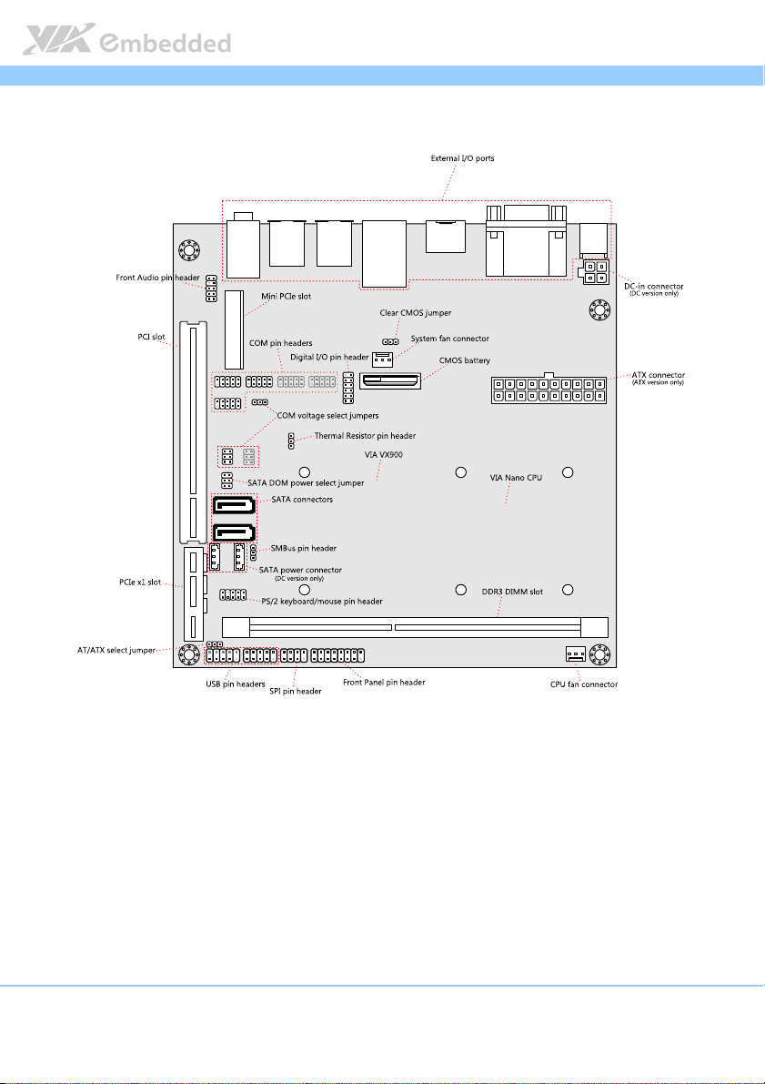
1.3. Layout Diagram
M860 User Manual
User Manual
M860M860
User ManualUser Manual
Figure
Figure 1111: Layout diagram of
: Layout diagram of the
Figure Figure
: Layout diagram of : Layout diagram of
the EPIA
EPIA----M860
the the
EPIAEPIA
M860 mainboard
mainboard
M860M860
mainboard mainboard
6
Page 19
EPIA
EPIA----M860
EPIAEPIA
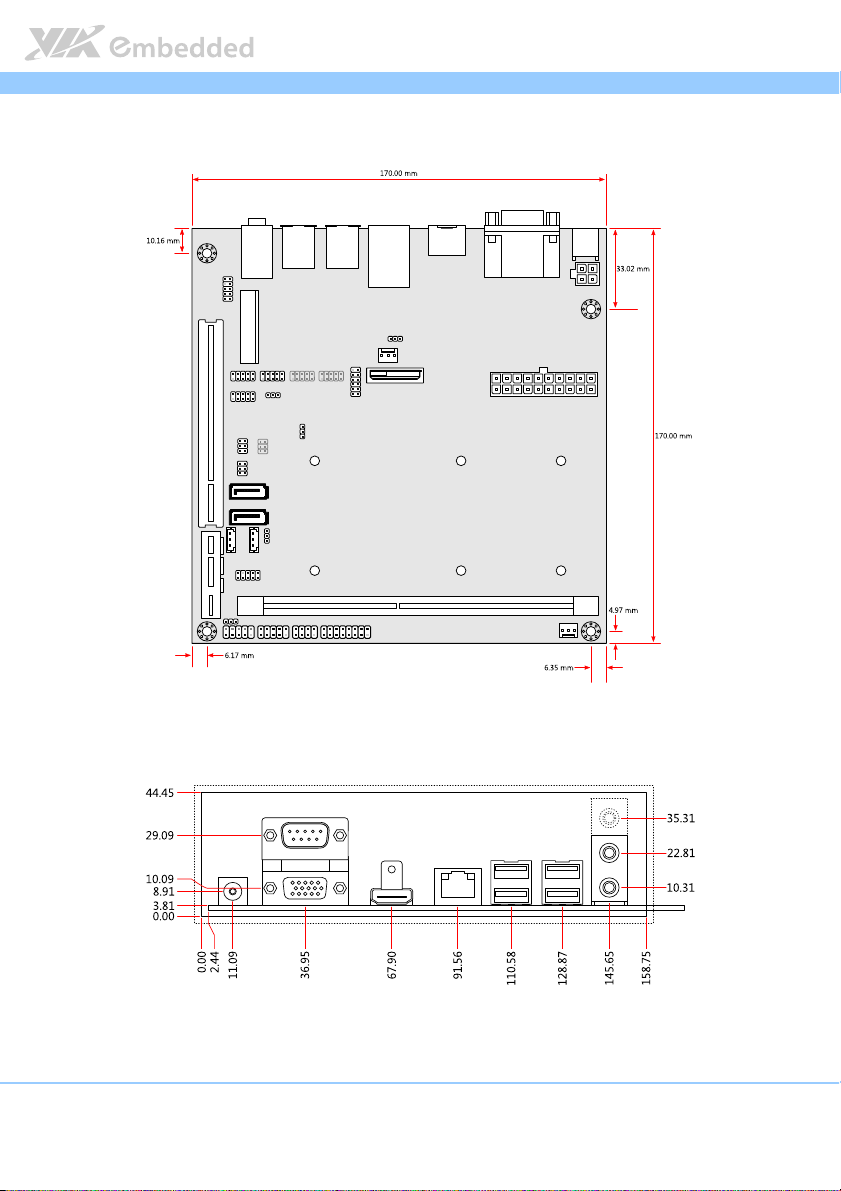
1.4. Product Dimensions
M860 User Manual
User Manual
M860M860
User ManualUser Manual
Figure
Figure 2222: Mounting holes and dimensions of
: Mounting holes and dimensions of the EPIA
Figure Figure
: Mounting holes and dimensions of: Mounting holes and dimensions of
the EPIA----M860
the EPIA the EPIA
M860 mainboard
M860M860
mainboard
mainboard mainboard
Figure
Figure 3333: External I/O port dimensions of the EPIA
: External I/O port dimensions of the EPIA----M860 mainboard
Figure Figure
: External I/O port dimensions of the EPIA: External I/O port dimensions of the EPIA
M860 mainboard
M860 mainboardM860 mainboard
7
Page 20
EPIA
EPIA----M860
EPIAEPIA
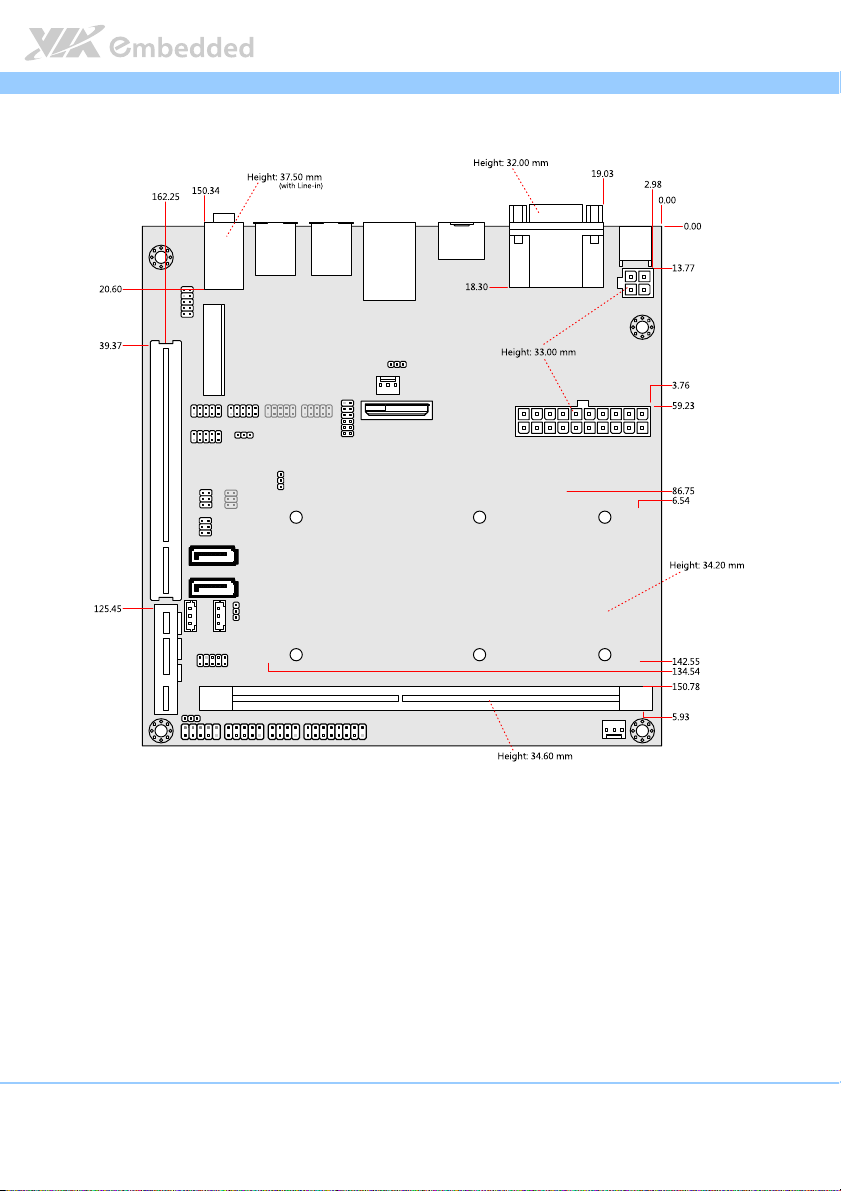
1.5. Height Distribution
M860 User Manual
User Manual
M860M860
User ManualUser Manual
Figure
Figure 4444: Height distribution of
: Height distribution of the
Figure Figure
: Height distribution of : Height distribution of
the EPIA
EPIA----M860
the the
EPIAEPIA
M860 mainboard
mainboard
M860M860
mainboard mainboard
8
Page 21
EPIA
2.
2. I/O Interface
I/O Interface
2.2.
I/O InterfaceI/O Interface
The VIA EPIA-M860 has a wide selection of interfaces integrated into the
board. It includes a selection of frequently used ports as part of the external
I/O coastline.
EPIA----M860
M860 User Manual
EPIAEPIA
M860M860
User Manual
User ManualUser Manual
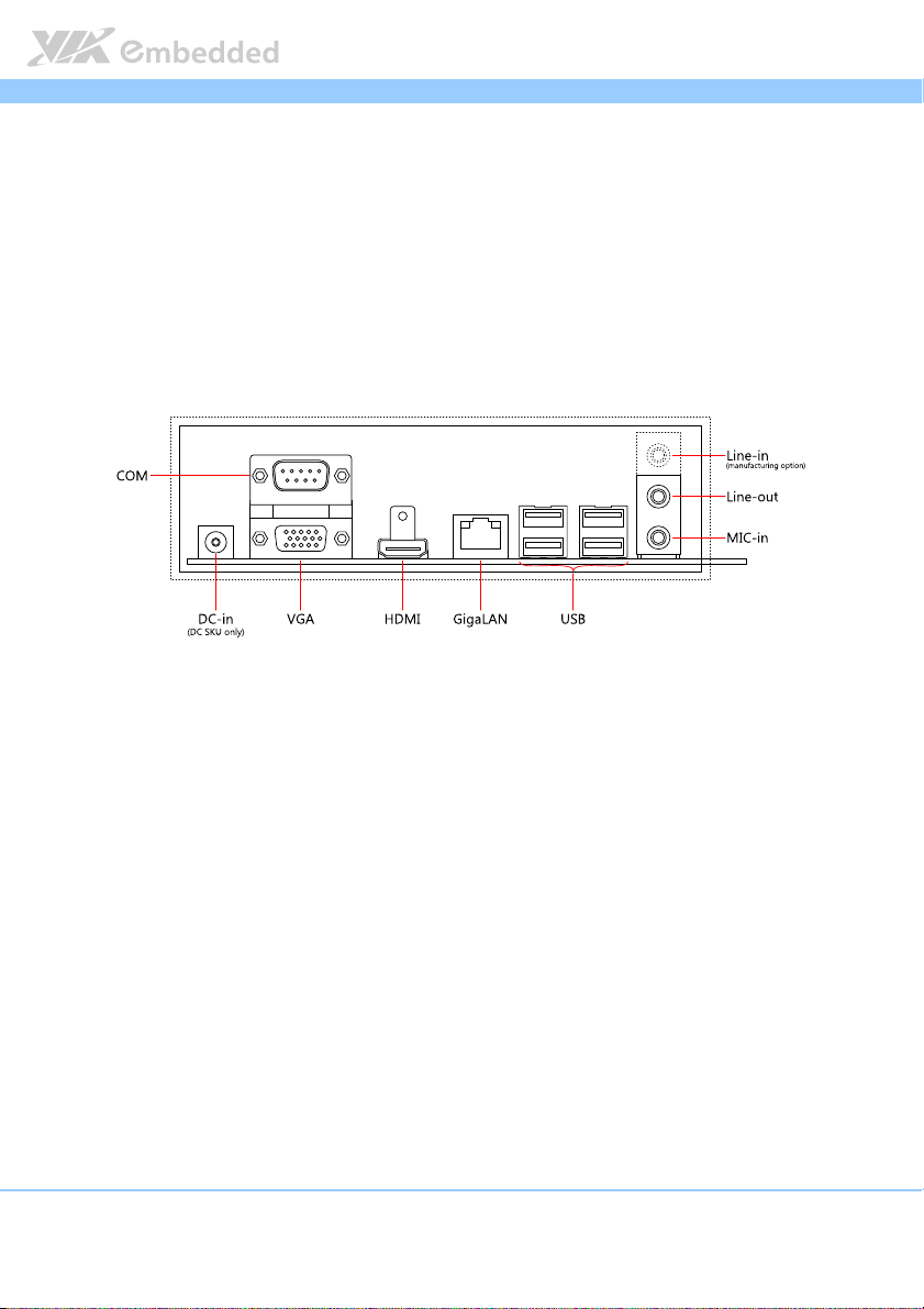
2.1. External I/O Ports
Figure
Figure 5555: External I/O ports
: External I/O ports
Figure Figure
: External I/O ports: External I/O ports
9
Page 22
EPIA
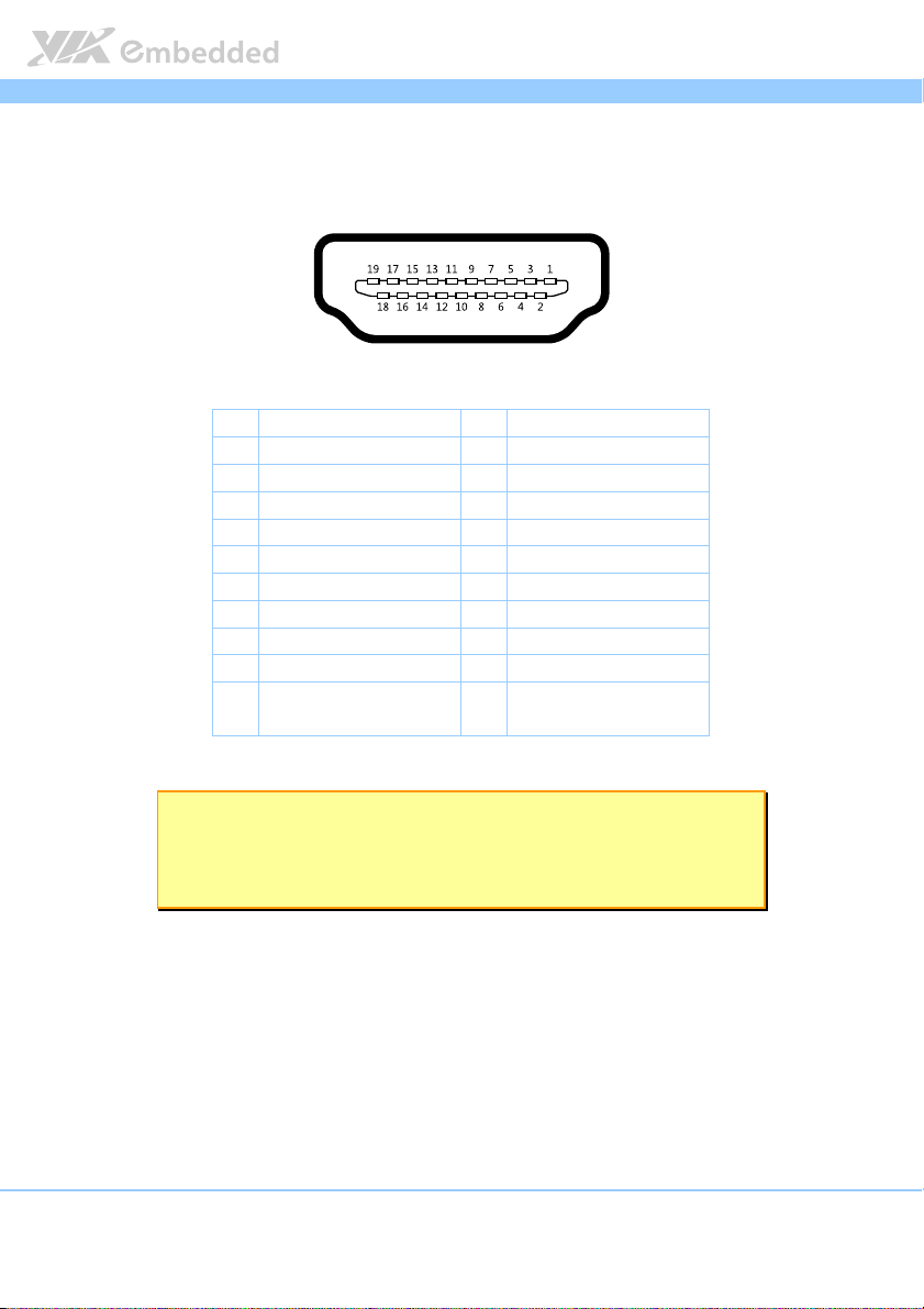
2.1.1. HDMI
®
Port
EPIA----M860
M860 User Manual
EPIAEPIA
M860M860
The integrated 19-pin HDMI® port uses an HDMI® Type A receptacle
®
connector. The pinout of the HDMI
Figure
Figure 6666: HDMI
Figure Figure
Table
Table 1111: HDMI
Table Table
®®®®
: HDMI
port pinout diagram
port pinout diagram
: HDMI: HDMI
port pinout diagram port pinout diagram
®®®®
: HDMI
port
port pinout
: HDMI: HDMI
port port
Pin
Pin
Signal
Signal Pin
PinPin
SignalSignal
1 TMDS Data2+ 2 TMDS Data2 Shield
3 TMDS Data2– 4 TMDS Data1+
5 TMDS Data1 Shield 6 TMDS Data1–
7 TMDS Data0+ 8 TMDS Data0 Shield
9 TMDS Data0– 10 TMDS Clock+
11 TMDS Clock Shield 12 TMDS Clock–
13 CEC 14 Reserved / HEC Data- 1
15 SCL 2 16 SDA 3
17 DDC/CEC/HEC Ground 18 +5 V Power 4
19 Hot Plug Detect and
HEC Data+
pinout
pinoutpinout
5
port is as shown below.
Pin
Signal
Signal
PinPin
SignalSignal
User Manual
User ManualUser Manual
Note:
Note:
Note:Note:
1. Pin 15: SCL is for I²C Serial Clock for DDC.
2. Pin 16: SDA is for I²C Serial Data Line for DDC.
3. Pin 18: max 50 mA
10
Page 23
EPIA
EPIA----M860
M860 User Manual
EPIAEPIA
M860M860
User Manual
User ManualUser Manual
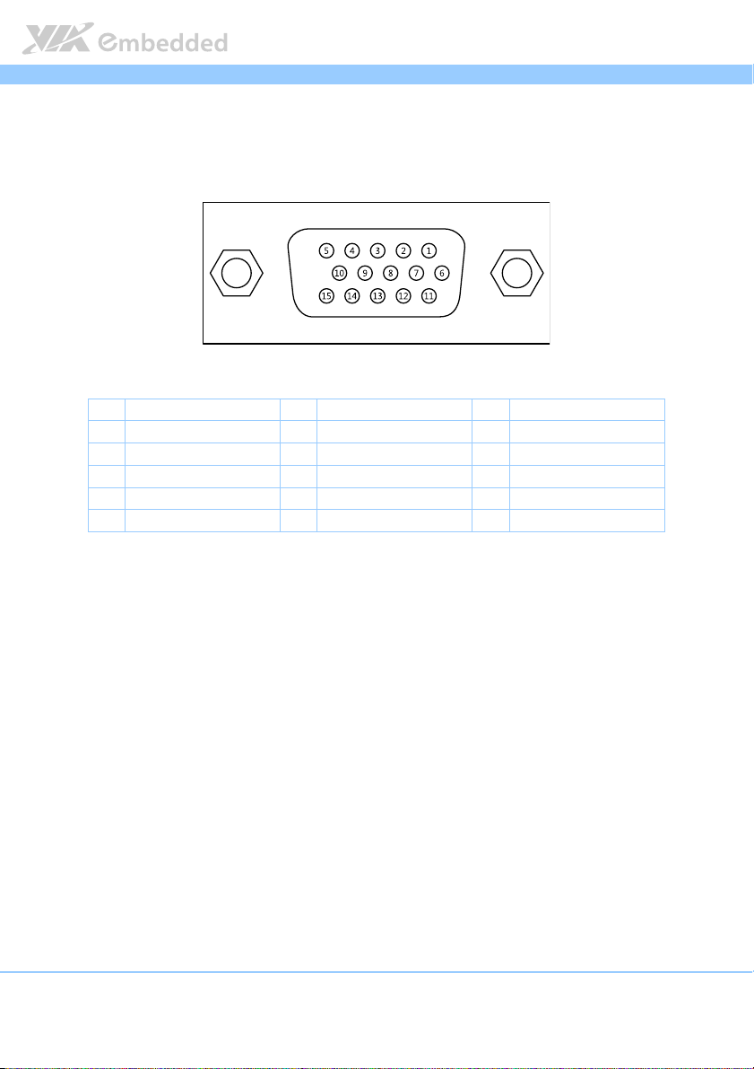
2.1.2. VGA Port
The integrated 15-pin VGA port uses a female DE-15 connector. The pinout of
the VGA port is as shown below.
Figure
Figure 7777: VGA port pinout diagram
: VGA port pinout diagram
Figure Figure
: VGA port pinout diagram: VGA port pinout diagram
Pin
Pin
Signal
Signal Pin
PinPin
SignalSignal
1 RED 6 GND 11 NC
2 GREEN 7 GND 12 SDA
3 BLUE 8 GND 13 HSync
4 NC 9 +5V 14 VSync
5 GND 10 GND 15 SCL
Table
Table 2222: VGA
: VGA port
port pinout
Table Table
: VGA : VGA
port port
pinout
pinoutpinout
Pin
Signal
Signal Pin
PinPin
SignalSignal
Pin
PinPin
Signal
Signal
SignalSignal
11
Page 24
EPIA
EPIA----M860
M860 User Manual
EPIAEPIA
M860M860
User Manual
User ManualUser Manual
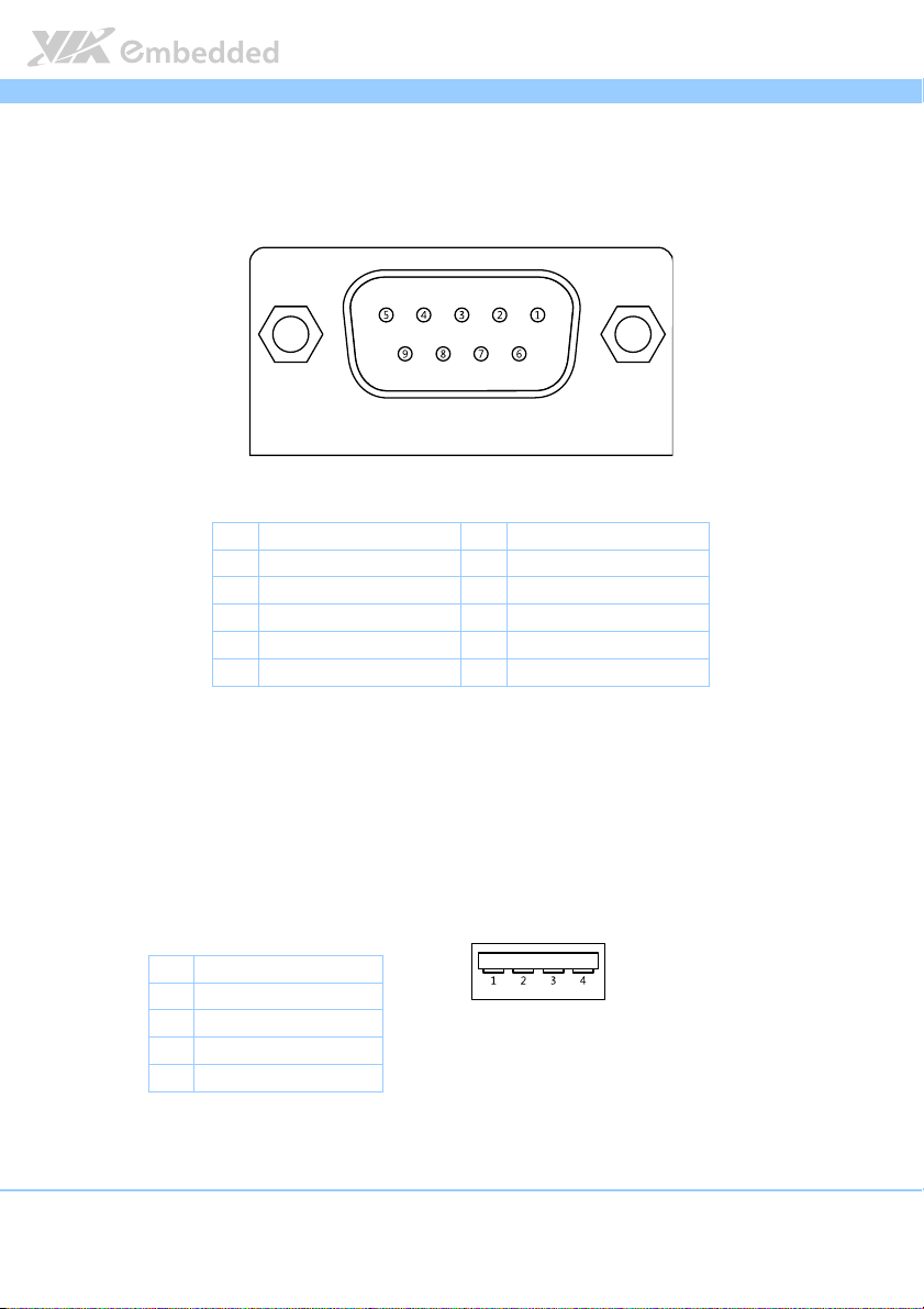
2.1.3. COM Port
The integrated 9-pin COM port uses a male DE-9 connector. The pinout of the
COM port is as shown below.
Figure
Figure 8888: COM port pinout diagram
: COM port pinout diagram
Figure Figure
: COM port pinout diagram: COM port pinout diagram
Pin
Pin
Signal
Table
Table 3333: COM
: COM port
Table Table
: COM : COM
Signal Pin
PinPin
SignalSignal
1 DCD 6 DSR
2 RxD 7 RTS
3 TxD 8 CTS
4 DTR 9 RI
5 GND
port pinout
pinout
port port
pinoutpinout
Pin
PinPin
Signal
Signal
SignalSignal
2.1.4. USB Ports
There are four integrated USB 2.0 ports separated into two USB port stacks.
Each USB port is using the USB Type A receptacle connector. The pinout of
the typical USB port is as shown below.
Pin
Pin
Signal
Signal
PinPin
SignalSignal
1 +5V
2 Data-
3 Data+
4 Ground
Table
Table 4444: USB
: USB port
port pinout
Table Table
: USB : USB
Figure
Figure 9999: USB port pinout diagram
: USB port pinout diagram
Figure Figure
: USB port pinout diagram: USB port pinout diagram
12
port port
pinout
pinoutpinout
Page 25
EPIA
EPIA----M860
M860 User Manual
EPIAEPIA
M860M860
User Manual
User ManualUser Manual
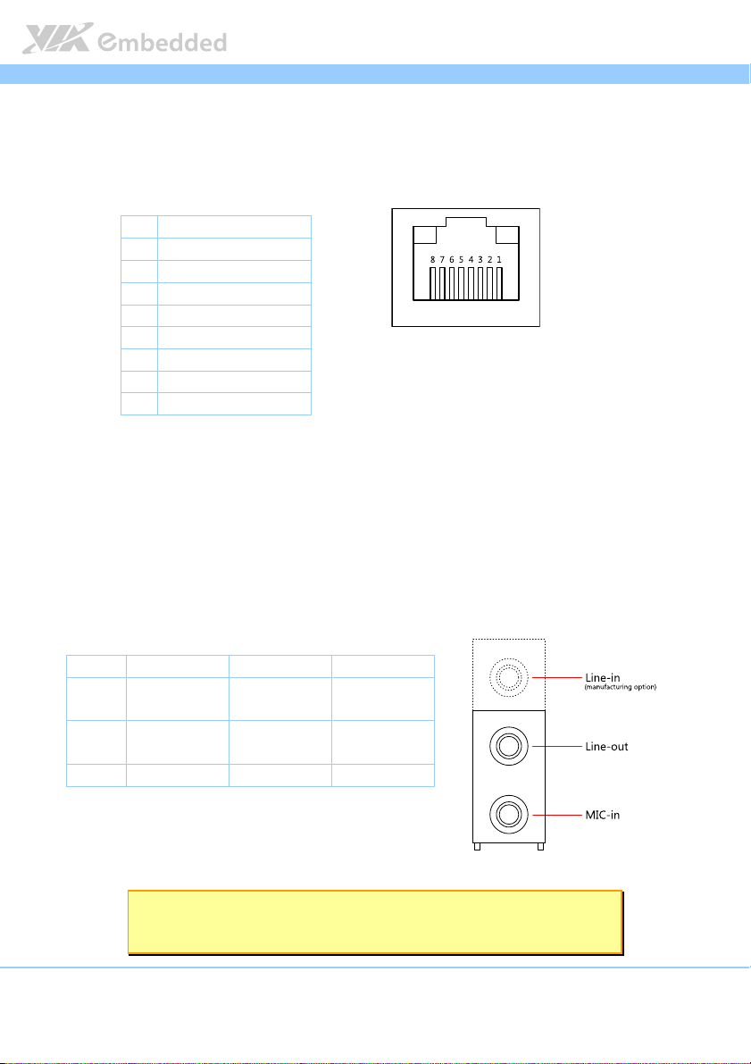
2.1.5. Gigabit Ethernet Port
The integrated 8-pin Gigabit Ethernet port is using an 8 Position 8 Contact
(8P8C) receptacle connector (commonly referred to as RJ45). The pinout of
the Gigabit Ethernet port is as shown below.
Pin
Pin
Signal
Signal
PinPin
SignalSignal
1 Signal pair 1+
2 Signal pair 1-
3 Signal pair 2+
4 Signal pair 3+
5 Signal pair 3-
6 Signal pair 2-
7 Signal pair 4+
8 Signal pair 4-
Table
Table 5555: Gigabit Ethernet port pinout
: Gigabit Ethernet port pinout
Table Table
: Gigabit Ethernet port pinout: Gigabit Ethernet port pinout
Figure
Figure 10
10: Gigabit Ethernet port pinout diagram
Figure Figure
: Gigabit Ethernet port pinout diagram
1010
: Gigabit Ethernet port pinout diagram: Gigabit Ethernet port pinout diagram
2.1.6. Audio Ports
There are three audio jack receptacles integrated into a single stack on the I/O
coastline. Each receptacle can fit a 3.5 mm Tip Ring Sleeve (TRS) connector to
enable connections to Line-in
1
, Line-out, and MIC-in.
Wiring
Wiring
WiringWiring
Tip Left channel
Ring Right channel
Sleeve Ground Ground Ground
Table
Table 6666: Audio jack receptacle pinout
Table Table
Figure
Figure 11
Figure Figure
Line
Line----in
in Line
LineLine
inin
in
in
: Audio jack receptacle pinout
: Audio jack receptacle pinout: Audio jack receptacle pinout
11: Audio jack receptacle stack
: Audio jack receptacle stack
1111
: Audio jack receptacle stack: Audio jack receptacle stack
Line----out
out MIC
LineLine
outout
Left channel Signal
Right channel +5V
MIC----in
MICMIC
in
inin
Note:
Note:
Note:Note:
1. Line-in is available as a manufacturing option. The default SKU does not include Line-in.
13
Page 26
EPIA
EPIA----M860
M860 User Manual
EPIAEPIA
M860M860
User Manual
User ManualUser Manual
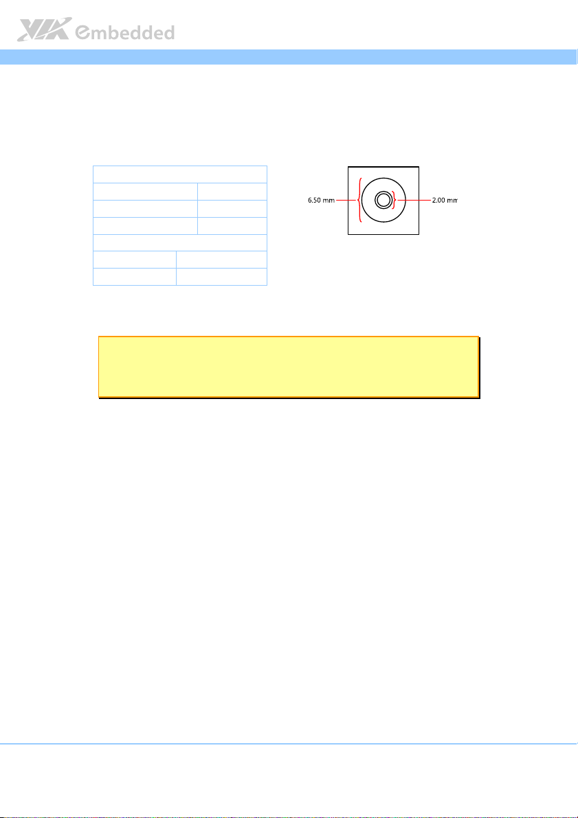
2.1.7. DC-in Jack
For the DC version of the mainboard, there is a coaxial power connector
adjacent to the COM/VGA connector stack. The specifications of the DC
coaxial power connector are shown below
Physical Specifications
Physical Specifications
Physical SpecificationsPhysical Specifications
Outer Diameter 6.50 mm
Inner Diameter 2.00 mm
Barrel Depth 8.80 mm
Electrical Specifications
Electrical Specifications
Electrical SpecificationsElectrical Specifications
Input Voltage 12 V
Input Current 5.0 A (max)
Table
Table 7777: DC
: DC----in coaxial connector specifications
Table Table
Figure
Figure 12
Figure Figure
in coaxial connector specifications
: DC: DC
in coaxial connector specificationsin coaxial connector specifications
12: DC
: DC----in coaxial connecto
in coaxial connectorrrr
1212
: DC: DC
in coaxial connectoin coaxial connecto
Note:
Note:
Note:Note:
The plug of the power adapter must have an inner diameter of 2.10 mm in order to fit the DC-in
coaxial connector properly.
14
Page 27
EPIA
EPIA----M860
M860 User Manual
EPIAEPIA
M860M860
User Manual
User ManualUser Manual
2.2. Onboard Connectors
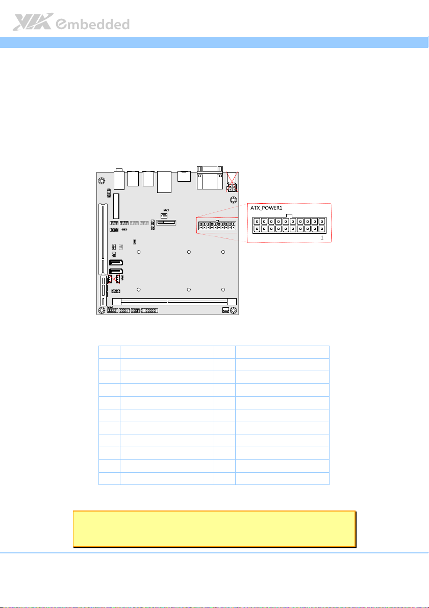
2.2.1. ATX Power Connector
For the ATX version of the mainboard, there is a 20-pin ATX power connector
onboard. The ATX power connector is labeled as “ATX_POWER1”. The
pinout of the ATX power connector is shown below.
Figure
Figure 13
13: ATX power connector
Figure Figure
: ATX power connector
1313
: ATX power connector: ATX power connector
Pin
Pin
Signal
Signal Pin
PinPin
SignalSignal
1 +3.3V 11 +3.3V
2 +3.3V 12 -12V
3 Ground 13 Ground
4 +5V 14 Power Supply On
5 Ground 15 Ground
6 +5V 16 Ground
7 Ground 17 Ground
8 Power OK 18 -5V
9 +5VSB 19 +5V
10 +12V 20 +5V
Table
Table 8888: ATX power connector pinout
: ATX power connector pinout
Table Table
: ATX power connector pinout: ATX power connector pinout
Note:
Note:
Note:Note:
The ATX version does not have the DC-in connectors or SATA power connectors.
15
Pin
PinPin
Signal
Signal
SignalSignal
Page 28
EPIA
EPIA----M860
M860 User Manual
EPIAEPIA
M860M860
User Manual
User ManualUser Manual
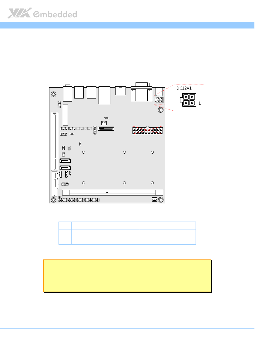
2.2.2. DC-in Power Connector
For the DC version of the mainboard, there is a DC-in power connecter in
addition to the DC-in coaxial power connector. This enables two methods for
delivering +12V to the mainboard. The pinout of the DC-in power connector
is shown below.
Figure
Figure 14
14: DC
: DC----in power connector
Figure Figure
Table
Table 9999: DC
Table Table
in power connector
1414
: DC: DC
in power connectorin power connector
Pin
Pin
Signal
Signal Pin
PinPin
SignalSignal
1 Ground 3 +12V
2 Ground 4 +12V
: DC----in power connector pinout
in power connector pinout
: DC: DC
in power connector pinoutin power connector pinout
Note:
Note:
Note:Note:
1. The DC-in version does not have the ATX power connector.
2. Max. power support is 80W.
Pin
PinPin
Signal
Signal
SignalSignal
16
Page 29
EPIA
EPIA----M860
M860 User Manual
EPIAEPIA
M860M860
User Manual
User ManualUser Manual
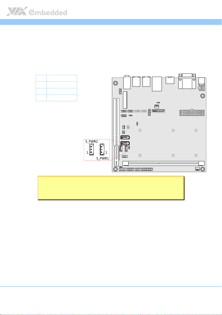
2.2.3. SATA Power Connector
For the DC version of the mainboard, there are two built-in SATA power
connectors. These connectors are required to power SATA hard drives. The
SATA power connectors are labeled as “S_PWR1” and “S_PWR2”. The pinout
of the SATA power connectors is shown below.
Pin
Pin
Signal
Signal
PinPin
SignalSignal
1 +5V
2 +12V
3 Ground
Table
Table 10
10: SATA power connector pinout
: SATA power connector pinout
Table Table
1010
: SATA power connector pinout: SATA power connector pinout
Figure
Figure 15
15: SATA power connector
Figure Figure
: SATA power connector
1515
: SATA power connector: SATA power connector
Note:
Note:
Note:Note:
The ATX version does not have the SATA power connector because power for SATA hard drives is
supplied from the ATX power supply.
17
Page 30
EPIA
EPIA----M860
M860 User Manual
EPIAEPIA
M860M860
User Manual
User ManualUser Manual
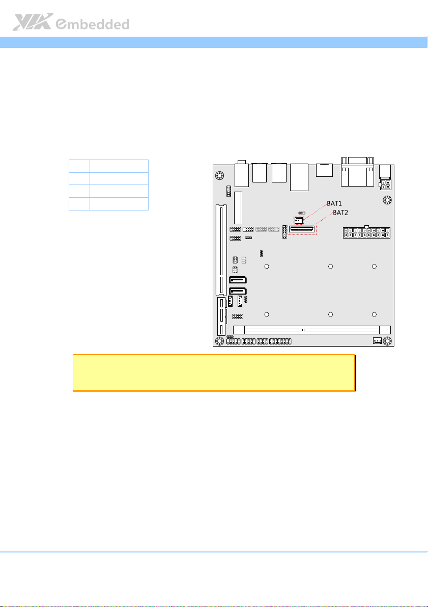
2.2.4. CMOS Battery Slot
Depending on the manufacturing option, the mainboard will either be
equipped with a CMOS battery slot or a 2-prong cable CMOS battery
connector. The default option is the CMOS battery slot, which is compatible
with CR2032 coin batteries. The CMOS battery slot is labeled as “BAT2”. If
equipped, the 2-prong cable CMOS battery connector will be labeled “BAT1”.
Pin
Pin
Signal
Signal
PinPin
SignalSignal
1 Ground
2 +3V
1
3
Ground
Table
Table 11
11: CMOS battery slot/connector pinout
: CMOS battery slot/connector pinout
Table Table
1111
: CMOS battery slot/connector pinout: CMOS battery slot/connector pinout
Figure
Figure 16
16: CMOS battery slot/connector
Figure Figure
: CMOS battery slot/connector
1616
: CMOS battery slot/connector: CMOS battery slot/connector
Note:
Note:
Note:Note:
1. The cable CMOS battery connector does not have a third pin.
18
Page 31

EPIA
EPIA----M860
M860 User Manual
EPIAEPIA
M860M860
User Manual
User ManualUser Manual
2.2.5. Front Panel Pin Header
The front panel pin header consists of 15 pins in a 16-pin block. Pin 15 is
keyed. The front panel pin header is labeled as “F_PANEL1”. It provides access
to system LEDs, power, reset, and system speaker. The pinout of the front
panel pin header is shown below.
Figure
Figure 17
17: Front panel pin header block
Figure Figure
Table
Table 12
Table Table
19
: Front panel pin header block
1717
: Front panel pin header block: Front panel pin header block
Pin
Pin
Signal
Signal Pin
PinPin
SignalSignal
1 +5VDUAL 2 +5V
3 +5VDUAL 4 SATA_LED
5 PWR_LED 6 PWR_BTN
7 +5V 8 Ground
9 NC 10 -RST_SW
11 NC 12 Ground
13 SPEAK 14 +5V
15 — 16 NC
12: Front
: Front panel pin header pinout
1212
panel pin header pinout
: Front : Front
panel pin header pinoutpanel pin header pinout
Pin
PinPin
Signal
Signal
SignalSignal
Page 32

EPIA
EPIA----M860
M860 User Manual
EPIAEPIA
M860M860
User Manual
User ManualUser Manual
2.2.6. SMBus Pin Header
The SMBus pin header consists of three pins. It is labeled as “SMBUS1”. The
pinout of the SMBus pin header is shown below.
Pin
Pin
Signal
Signal
PinPin
SignalSignal
1 SMBCK
2 SMBDT
3 Ground
Table
Table 13
13: SMBus pin header
: SMBus pin header pinout
Table Table
1313
: SMBus pin header : SMBus pin header
Figure
Figure 18
18: SMBus pin header
Figure Figure
: SMBus pin header
1818
: SMBus pin header: SMBus pin header
pinout
pinoutpinout
2.2.7. Thermal Resistor Pin Header
The thermal resistor pin header consists of three pins. The pin header is
labeled as “J5”. The pin out of the thermal resistor pin header is shown below.
Pin
Pin
Sign
Signal
SignSign
al
alal
pin header pinout
pin header pin header
pin header
pin headerpin header
pinout
pinoutpinout
PinPin
1 TMPIN2
2 TMPIN2
3 HWMGND
Table
Table 14
14: Thermal resistor
: Thermal resistor pin header
Table Table
1414
: Thermal resistor : Thermal resistor
Figure
Figure 19
19: Thermal resistor
Figure Figure
: Thermal resistor pin header
1919
: Thermal resistor : Thermal resistor
20
Page 33

EPIA
EPIA----M860
M860 User Manual
EPIAEPIA
M860M860
User Manual
User ManualUser Manual
2.2.8. Fan Connectors
There are two fan connectors on board: one for the CPU and one for the
chassis. The fan connectors are the standard 3-prong fan connectors. The
pinout of the fan connectors is shown below.
CPU fan
CPU fan
CPU fanCPU fan
Pin
Pin
Signal
Signal
PinPin
SignalSignal
1 F_IO2
2 F_PWM2
3 Ground
System fan
System fan
System fanSystem fan
Pin
Pin
Signal
Signal
PinPin
SignalSignal
1 F_IO1
2 F_PWM1
3 Ground
Table
Table 15
15:
: FFFFan connector pinout
Table Table
Figure
Figure 20
Figure Figure
an connector pinoutssss
1515
: :
an connector pinoutan connector pinout
20:
: FFFFan connectors
an connectors
2020
: :
an connectorsan connectors
21
Page 34

EPIA
EPIA----M860
M860 User Manual
EPIAEPIA
M860M860
User Manual
User ManualUser Manual
2.2.9. SATA Connectors
The two SATA connectors on board can support up to 3 Gb/s transfer speeds.
The SATA connectors are labeled as “SATA1” and “SATA2”. The pinout of the
SATA connectors are as shown below.
SATA1
SATA1
SATA1SATA1
Pin
Pin
Signal
Signal
PinPin
SignalSignal
1 Ground
2 STXP_1
3 STXN_1
4 Ground
5 SRXN_1
6 SRXP_1
7 SATA1_+5V
SATA2
SATA2
SATA2SATA2
Pin
Pin
Signal
Signal
PinPin
SignalSignal
1 Ground
2 STXP_2
3 STXN_2
4 Ground
5 SRXN_2
6 SRXP_2
7 SATA2_+5V
Table
Table 16
16: SATA connec
: SATA connector pinouts
Table Table
1616
: SATA connec: SATA connec
Figure
Figure 21
21: SATA connectors
Figure Figure
: SATA connectors
2121
: SATA connectors: SATA connectors
tor pinouts
tor pinoutstor pinouts
22
Page 35

EPIA
EPIA----M860
M860 User Manual
EPIAEPIA
M860M860
User Manual
User ManualUser Manual
2.2.10. USB Pin Headers
The mainboard has two USB pin header blocks that support up to three USB
2.0 ports. The pin header blocks are labeled as “USB_3” and “USB_4”. USB_4
only supports one USB 2.0 port. The pinout of the USB pin headers are shown
below.
Figure
Figure 22
22: USB pin headers
Figure Figure
: USB pin headers
2222
: USB pin headers: USB pin headers
USB_3
USB_3
USB_3USB_3
Pin
Pin
Signal
Signal Pin
PinPin
SignalSignal
1 +5CDUAL 2 +5CDUAL
3 USBD_T3- 4 USBD_T2-
5 USBD_T3+ 6 USBD_T2+
7 Ground 8 Ground
9 — 10 Ground
Pin
PinPin
Signal
Signal
SignalSignal
USB_4
USB_4
USB_4USB_4
Pin
Pin
Signal
Signal Pin
PinPin
SignalSignal
1 +5CDUAL 21 Reserved
3 USBD_T6- 41 Reserved
5 USBD_T6+ 61 Reserved
7 Ground 81 Reserved
9 — 10
Pin
PinPin
1
Signal
Signal
SignalSignal
Reserved
Note:
Note:
Note:Note:
1. The USB signals in pins 2, 4, 6, 8, and 10 in the USB_4 pin header block are reserved for the Mini
PCIe slot.
23
Page 36

EPIA
EPIA----M860
M860 User Manual
EPIAEPIA
M860M860
User Manual
User ManualUser Manual
2.2.11. COM Pin Headers
There are a total of three COM pin headers on the mainboard1. Each COM pin
header supports the RS-232 standard. The pin headers are labeled as “COM2”,
“COM3”, and “COM4”. All of the COM pin headers can support +5V or +12V.
See page 32 for details on setting the voltage. The pinout of the COM pin
headers are shown below.
Figure
Figure 23
23: COM pin headers
Figure Figure
: COM pin headers
2323
: COM pin headers: COM pin headers
Pin
Pin
Signal
Signal Pin
PinPin
SignalSignal
1 COM_DCD 2 COM_RXD
3 COM_TXD 4 COM_DTR
5 Ground 6 COM_DSR
7 COM_RTS 8 COM_CTS
9 COM_RI 10 —
Table
Table 17
17: COM pin header pinout
: COM pin header pinout
Table Table
1717
: COM pin header pinout: COM pin header pinout
Note:
Note:
Note:Note:
1. Two additional COM pin headers can be added as a manufacturing option. The additional COM pin
headers will be labeled as “COM5” and “COM6”.
24
Pin
PinPin
Signal
Signal
SignalSignal
Page 37

EPIA
EPIA----M860
M860 User Manual
EPIAEPIA
M860M860
User Manual
User ManualUser Manual
2.2.12. PS/2 Keyboard and Mouse Pin Header
The mainboard has a pin header for a PS/2 keyboard and mouse. The pin
header is labeled as “JKB/MS1”. The pinout of the pin header is shown below.
Figure
Figure 24
24: PS/2 keyboard and mouse pin header
Figure Figure
: PS/2 keyboard and mouse pin header
2424
: PS/2 keyboard and mouse pin header: PS/2 keyboard and mouse pin header
Pin
Pin
Signal
Signal Pin
PinPin
SignalSignal
1 VCCE 2 VCCE
3 NC 4 —
5 Ground 6 Ground
7 KB_DT 8 MS_DT
9 KB_CK 10 MS_CK
Table
Table 18
18: PS/2 keyboard and mouse pin header pinout
: PS/2 keyboard and mouse pin header pinout
Table Table
1818
: PS/2 keyboard and mouse pin header pinout: PS/2 keyboard and mouse pin header pinout
25
Pin
PinPin
Signal
Signal
SignalSignal
Page 38

EPIA
EPIA----M860
M860 User Manual
EPIAEPIA
M860M860
User Manual
User ManualUser Manual
2.2.13. Front Audio Pin Header
In addition to the TRS audio jacks on the external I/O coastline, the mainboard
has a pin header for Line-out and MIC-in. The pin header is labeled as
“F_AUDIO1”. The pinout of the pin header is shown below.
Figure
Figure 25
25:
: Front audio pin header
Figure Figure
Front audio pin header
2525
: :
Front audio pin headerFront audio pin header
Pin
Pin
Signal
PinPin
1 MIC2IN_L 2 Ground
3 MIC2IN_R 4 Ground
5 HPOUTR 6 MIC2_JD
7 F_AUDIO_SENSE 8 —
9 HPOUTl 10 HPOUT_JD
Table
Table 19
19: Front audio pin header pinout
: Front audio pin header pinout
Table Table
1919
: Front audio pin header pinout: Front audio pin header pinout
Signal Pin
SignalSignal
Pin
PinPin
Signal
Signal
SignalSignal
26
Page 39

EPIA
EPIA----M860
M860 User Manual
EPIAEPIA
M860M860
User Manual
User ManualUser Manual
2.2.14. Digital I/O Pin Header
The onboard Digital I/O pin header supports up to four GPO and four GPI
signals. The pin header is labeled as “DIO1”. The pinout of the pin header is
shown below.
Figure
Figure 26
26: Digial I/O pin header
Figure Figure
: Digial I/O pin header
2626
: Digial I/O pin header: Digial I/O pin header
Pin
Pin
Signal
Table
Table 20
20: Digital I/O pin header pinout
: Digital I/O pin header pinout
TableTable
2020
: Digital I/O pin header pinout: Digital I/O pin header pinout
Signal Pin
PinPin
SignalSignal
1 5V_DIO 2 12V_DIO
3 GPO_23 4 GPI_03
5 GPO_22 6 GPI_02
7 GPO_21 8 GPI_01
9 GPO_20 10 GPI_00
11 Ground 12 —
Pin
PinPin
Signal
Signal
SignalSignal
27
Page 40

EPIA
EPIA----M860
M860 User Manual
EPIAEPIA
M860M860
User Manual
User ManualUser Manual
2.2.15. SPI Pin Header
The mainboard has one 8-pin SPI pin header. The pin header is labeled as
“SPI1”. The pinout of the pin header is shown below.
Figure
Figure 27
27: SPI pin header
Figure Figure
: SPI pin header
2727
: SPI pin header: SPI pin header
PPPPin
in
Signal
Table
Table 21
21: SPI pin header pinout
: SPI pin header pinout
Table Table
2121
: SPI pin header pinout: SPI pin header pinout
Signal Pin
inin
SignalSignal
1 SPIVCC 2 Ground
3 MSPISS0 4 MSPICLK
5 MSPIDI 6 MSPIDO
7 — 8 -PCIRST
Pin
PinPin
Signal
Signal
SignalSignal
28
Page 41

EPIA
3.
3. Jumpers and Switches
Jumpers and Switches
3.3.
Jumpers and SwitchesJumpers and Switches
EPIA----M860
M860 User Manual
EPIAEPIA
M860M860
User Manual
User ManualUser Manual
3.1. AT/ATX Mode
For the ATX version of the EPIA-M860, there is a jumper that can enable to
mainboard to switch between two power modes: AT and ATX. The jumper is
labeled as “J10”. The jumper settings are shown below.
Figure
Figure 28
28: AT/ATX mode jumper
Figure Figure
Table
Table 22
Table Table
The recommended setting of the jumper is the ATX mode. For the DC version
of the board, always keep the jumper on the ATX mode setting.
: AT/ATX mode jumper
2828
: AT/ATX mode jumper: AT/ATX mode jumper
Setting
Setting Pin 1
SettingSetting
ATX mode On On Off
AT mode Off On On
22: AT/ATX mode jumper
: AT/ATX mode jumper settings
2222
: AT/ATX mode jumper : AT/ATX mode jumper
settings
settingssettings
Pin 1 Pin 2
Pin 1Pin 1
Pin 2 Pin 3
Pin 2Pin 2
Pin 3
Pin 3Pin 3
29
Page 42

EPIA
EPIA----M860
M860 User Manual
EPIAEPIA
M860M860
User Manual
User ManualUser Manual
3.2. SATA DOM Power Select Jumper
The SATA connectors (see page 22) can be used to support Disk-on-Module
th
flash drives. When the jumpers are set, +5V will be delivered to the 7
the SATA connectors. The jumper settings are shown below.
pin of
Figure
Figure 29
29: SATA
: SATA DOM voltage select jumper
Figure Figure
2929
Table
Table 23
23: SATA DOM voltage sel
Table Table
2323
DOM voltage select jumper
: SATA: SATA
DOM voltage select jumper DOM voltage select jumper
SATA1 Setting
SATA1 Setting Pin 1
SATA1 SettingSATA1 Setting
DOM support On On Off
Regular (default) Off On On
SATA2 Setting
SATA2 Setting Pin 2
SATA2 SettingSATA2 Setting
DOM support On On Off
Regular (default) Off On On
: SATA DOM voltage select jumper settings
: SATA DOM voltage sel: SATA DOM voltage sel
ect jumper settings
ect jumper settingsect jumper settings
Pin 1 Pin 3
Pin 1Pin 1
Pin 2 Pin 4
Pin 2Pin 2
Pin 3 Pin 5
Pin 3Pin 3
Pin 4 Pin 6
Pin 4Pin 4
Pin 5
Pin 5Pin 5
Pin 6
Pin 6Pin 6
30
Page 43

EPIA
EPIA----M860
M860 User Manual
EPIAEPIA
M860M860
User Manual
User ManualUser Manual
3.3. Clear CMOS Jumper
The onboard CMOS RAM stores system configuration data and has an onboard
battery power supply. To reset the CMOS settings, set the jumper on pins 2
and 3 while the system is off. Return the jumper to pins 1 and 2 afterwards.
Setting the jumper while the system is on will damage the mainboard. The
default setting is on pins 1 and 2.
Figure
Figure 30
30: CLEAR CMOS jumper
Figure Figure
Tabl
Table
TablTabl
: CLEAR CMOS jumper
3030
: CLEAR CMOS jumper: CLEAR CMOS jumper
Setting
Setting Pin 1
SettingSetting
Regular (default) On On Off
Clear CMOS Off On On
e 24
24: CLEAR CMOS jumper settings
: CLEAR CMOS jumper settings
e e
2424
: CLEAR CMOS jumper settings: CLEAR CMOS jumper settings
Note:
Note:
Note:Note:
Except when clearing the RTC RAM, never remove the cap from the CLEAR_CMOS jumper default
position. Removing the cap will cause system boot failure. Avoid clearing the CMOS while the system
is on; it will damage the mainboard.
Pin 1 Pin 2
Pin 1Pin 1
Pin 2 Pin 3
Pin 2Pin 2
Pin 3
Pin 3Pin 3
31
Page 44

EPIA
EPIA----M860
M860 User Manual
EPIAEPIA
M860M860
User Manual
User ManualUser Manual
3.4. COM Voltage Select Jumpers
Each of the additional COM ports (available through the onboard COM pin
headers, see page 24) can support both +5V and +12V. COM2 has its own pin
header block. COM3 and COM4 share a single pin header block. COM5 and
COM6 also share a single pin header block.
3.4.1. COM2 Voltage Select Jumper
The voltage for COM2 is controlled by the jumper labeled as “J6”. The
voltage can be either +5V or +12V. +5V is the default setting. The jumper
settings are shown below.
Setting
Setting Pin 1
SettingSetting
+5V (default) On On Off
+12V Off On On
Table
Table 25
25: COM2 voltage select jumper settings
: COM2 voltage select jumper settings
Table Table
2525
: COM2 voltage select jumper settings: COM2 voltage select jumper settings
Pin 1 Pin 2
Pin 1Pin 1
Pin 2 Pin 3
Pin 2Pin 2
Pin 3
Pin 3Pin 3
Figure
Figure 31
31: Voltage select jumpers for COM2
Figure Figure
: Voltage select jumpers for COM2 –––– COM6
3131
: Voltage select jumpers for COM2: Voltage select jumpers for COM2
COM6
COM6 COM6
32
Page 45

EPIA
EPIA----M860
M860 User Manual
EPIAEPIA
M860M860
User Manual
User ManualUser Manual
3.4.2. COM3 and COM4 Voltage Select Jumper
The voltage for COM3 and COM4 is controlled by the jumper labeled as “J7”.
Refer to Figure 31 for the location of the jumper.
The voltage can be either +5V or +12V. +5V is the default setting. The odd
pin numbers correspond to COM3. The even pin numbers correspond to
COM4. The jumper settings are shown below.
COM3
COM3 Setting
COM3COM3
+5V (default) On On Off
+12V Off On On
COM4
COM4 Setting
COM4COM4
+5V (default) On On Off
+12V Off On On
Table
Table 26
26: Jumper settings for COM3 and COM4
: Jumper settings for COM3 and COM4
Table Table
2626
: Jumper settings for COM3 and COM4: Jumper settings for COM3 and COM4
Setting Pin 1
Setting Setting
Setting Pin 2
Setting Setting
Pin 1 Pin 3
Pin 1Pin 1
Pin 2 Pin 4
Pin 2Pin 2
Pin 3 Pin 5
Pin 3Pin 3
Pin 4 Pin 6
Pin 4Pin 4
Pin 5
Pin 5Pin 5
Pin 6
Pin 6Pin 6
3.4.3. COM5 and COM6 Voltage Select Jumper
The voltage for COM5 and COM6 is controlled by the jumper labeled as “J8”.
Refer to Figure 31 for the location of the jumper.
The voltage can be either +5V or +12V. +5V is the default setting. The odd
pin numbers correspond to COM5. The even pin numbers correspond to
COM6. The jumper settings are shown below.
COM
COM5555 Setting
COMCOM
+5V (default) On On Off
+12V Off On On
COM
COM6666 Setting
COMCOM
+5V (default) On On Off
+12V Off On On
Table
Table 27
27: Jumper settings for COM5 and COM6
: Jumper settings for COM5 and COM6
Table Table
2727
: Jumper settings for COM5 and COM6: Jumper settings for COM5 and COM6
Note:
Note:
Note:Note:
If the mainboard is not equipped with COM5 and COM6, then the J8 jumper will not be on the
mainboard either.
Setting Pin 1
Setting Setting
Setting Pin 2
Setting Setting
Pin 1 Pin 3
Pin 1Pin 1
Pin 2 Pin 4
Pin 2Pin 2
Pin 3 Pin 5
Pin 3Pin 3
Pin 4 Pin 6
Pin 4Pin 4
Pin 5
Pin 5Pin 5
Pin 6
Pin 6Pin 6
33
Page 46

EPIA
EPIA----M860
EPIAEPIA
M860 User Manual
User Manual
M860M860
User ManualUser Manual
34
Page 47

EPIA
4.
4. Expansion Slots
Expansion Slots
4.4.
Expansion SlotsExpansion Slots
EPIA----M860
M860 User Manual
EPIAEPIA
M860M860
User Manual
User ManualUser Manual
4.1. DDR3 Memory Slot
The DDR3 memory slot can accommodate up to 4 GB of 1066 MHz memory.
The location of the DDR3 memory slot is as shown below.
Figure
Figure 32
32: DDR3 memory slot
Figure Figure
35
: DDR3 memory slot
3232
: DDR3 memory slot: DDR3 memory slot
Page 48

EPIA
EPIA----M860
M860 User Manual
EPIAEPIA
M860M860
User Manual
User ManualUser Manual
4.1.1. Installing a Memory Module
Step 1
Step 1
Step 1Step 1
Disengage the locking clasps at both ends of the memory slot.
Figure
Figure 33
33: Installing memory 1
Figure Figure
Step 2
Step 2
Step 2Step 2
Align the notch on the bottom of the DDR3 memory module with the notch
wedge in the slot.
Step 3
Step 3
Step 3Step 3
: Installing memory 1
3333
: Installing memory 1: Installing memory 1
Slide the DDR3 memory module into the side grooves and push the module
into the slot until the locking clasps snap into the closed position.
Figure
Figure 34
34: Installing memory 2
Figure Figure
: Installing memory 2
3434
: Installing memory 2: Installing memory 2
36
Page 49

EPIA
EPIA----M860
EPIAEPIA
4.1.2. Removing a Memory Module
Step 1
Step 1
Step 1Step 1
Disengage the locking clasps on both sides of the memory slot.
Figure
Figure 35
35: Removing memory 1
Figure Figure
Step 2
Step 2
Step 2Step 2
Remove the memory module.
: Removing memory 1
3535
: Removing memory 1: Removing memory 1
M860 User Manual
User Manual
M860M860
User ManualUser Manual
Figure
Figure 36
36: Removing memory 2
Figure Figure
Step 3
Step 3
Step 3Step 3
: Removing memory 2
3636
: Removing memory 2: Removing memory 2
Move the locking clasps into the closed position.
37
Page 50

EPIA
EPIA----M860
M860 User Manual
EPIAEPIA
M860M860
User Manual
User ManualUser Manual
4.2. Mini PCIe Slot
The Mini PCIe slot is compatible with all PCIe 2.0 Mini Cards: full-length and
half-length. The location of the Mini PCIe slot is shown below.
Figure
Figure 37
37: Mini PCIe slot
Figure Figure
: Mini PCIe slot
3737
: Mini PCIe slot: Mini PCIe slot
38
Page 51

EPIA
EPIA----M860
M860 User Manual
EPIAEPIA
M860M860
User Manual
User ManualUser Manual
4.3. PCI Express Slot
The onboard PCI Express slot is located adjacent to the PCI slot. The PCI
Express slot provides support for 1-lane cards. Due to the orientation of the
slot, a riser card module
install the riser card module. The location of the PCI Express slot is shown
below.
1
must be used. See page 89 for details on how to
Figure
Figure 38
38: PCI Express slot
Figure Figure
: PCI Express slot
3838
: PCI Express slot: PCI Express slot
Note:
Note:
Note:Note:
1. The optional riser card module is PCIE-03. PCIE-03 is a combination riser card that connects to both
the PCI Express and PCI slots.
39
Page 52

EPIA
EPIA----M860
M860 User Manual
EPIAEPIA
M860M860
User Manual
User ManualUser Manual
4.4. PCI Slot
The onboard PCI slot supports 5V 32-bit PCI cards. It is not compatible with
PCI cards requiring 3.3V signaling. The PCI slot is located adjacent to the PCI
Express slot. Using the PCI slot will negate the use of the PCI Express slot
unless the optional PCIE-03 riser card module is used. The location of the PCI
slot is shown below.
The orientation of PCI cards can be changed from vertical to horizontal using a
riser card module. Compatible optional riser card modules include the
following models: EXT-PCI-01 and PCIE-03.
The EXT-PCI-01 module enables the PCI slot to support two PCI expansion
cards horizontally. The PCIE-03 module enables the PCI slot to support one
PCI card and one PCIe card horizontally. See page 89 for details on how to
install the riser card module.
Figure
Figure 39
39: PCI slot
Figure Figure
: PCI slot
3939
: PCI slot: PCI slot
40
Page 53

EPIA
5.
5. Hardware Installation
Hardware Installation
5.5.
Hardware InstallationHardware Installation
EPIA----M860
M860 User Manual
EPIAEPIA
M860M860
User Manual
User ManualUser Manual
5.1. Installing into a Chassis
The EPIA-M860 can be fitted into any chassis that has the mounting holes
compatible with the standard Mini-ITX mounting hole locations. Additionally,
the chassis must meet the minimum height requirements for specified areas of
the mainboard.
If a riser card module is being used, the chassis will need to accommodate the
additional space requirements.
5.1.1. Suggested minimum chassis dimensions
The figure below shows the suggested minimum space requirements that a
chassis should have in order to work well with the EPIA-M860.
Figure
Figure 40
40: Suggested minimum chassis dimensions
Figure Figure
: Suggested minimum chassis dimensions
4040
: Suggested minimum chassis dimensions: Suggested minimum chassis dimensions
41
Page 54

EPIA
EPIA----M860
M860 User Manual
EPIAEPIA
M860M860
User Manual
User ManualUser Manual
Each side of the mainboard should have a buffer zone from the internal wall
of the chassis. The side of the mainboard that accommodates the I/O coastline
should have a buffer of 1.00 mm. The side on the opposite end of the I/O
coastline should have a buffer of at least 5.00 mm. The two sides adjacent to
the I/O coastline should have at least a 10.00 mm buffer.
For the side that is close to the PCI slot, the buffer should be at least 100.00
mm if a riser card module will be used.
5.1.2. Suggested minimum chassis height
The figure below shows the suggested minimum height requirements for the
internal space of the chassis. It is not necessary for the internal ceiling to be
evenly flat. What is required is that the internal ceiling height must be strictly
observed for each section that is highlighted. The highest part of the ceiling
will be above the PCI and PCIe slots.
Figure
Figure 41
41: Suggested minimum internal chassis ceiling height
Figure Figure
: Suggested minimum internal chassis ceiling height
4141
: Suggested minimum internal chassis ceiling height: Suggested minimum internal chassis ceiling height
42
Page 55

EPIA
EPIA----M860
M860 User Manual
EPIAEPIA
M860M860
User Manual
User ManualUser Manual
5.1.3. Suggested keepout areas
The figure below shows the areas of the mainboard that is highly suggested to
leave unobstructed.
Figure
Figure 42
42: Suggested keepout areas
Figure Figure
: Suggested keepout areas
4242
: Suggested keepout areas: Suggested keepout areas
43
Page 56

Page 57

EPIA
6.
6. BIOS Setup
BIOS Setup Utility
6.6.
BIOS Setup BIOS Setup
Utility
UtilityUtility
EPIA----M860
EPIAEPIA
6.1. Entering the BIOS Setup Utility
M860 User Manual
User Manual
M860M860
User ManualUser Manual
Power on the computer and press Delete
sequence to enter the BIOS Setup Utility. If the entry point has passed, restart
the system and try again.
Delete during the beginning of the boot
DeleteDelete
6.2. Control Keys
Up
Up Move up one row
UpUp
Down
Down Move down one row
DownDown
Left
Left Move to the left in the navigation bar
LeftLeft
Right
Right Move to the right in the navigation bar
RightRight
Enter
Enter Access the highlighted item
EnterEnter
Esc
Esc Jumps to the Exit screen or returns to the previous screen
EscEsc
++++1 Increase the numeric value
1
Decrease the numeric value
----
2
F1
F1 General help
F1F1
F7
F7 Discard changes
F7F7
F9
F9 Load optimized defaults
F9F9
F10
F10 Save all the changes and exit
F10F10
Note:
Note:
Note:Note:
1. Must be pressed using the 10-key pad.
2. The General help contents are only for the Status Page and Option Page setup menus.
45
Page 58

EPIA
EPIA----M860
M860 User Manual
EPIAEPIA
M860M860
User Manual
User ManualUser Manual
6.3. Getting Help
The BIOS Setup Utility provides a “General Help” screen. This screen can be
accessed at any time by pressing F1
using and navigating the BIOS Setup Utility. Press Esc
F1. The help screen displays the keys for
F1F1
Esc to exit the help screen.
EscEsc
6.4. System Overview
The System Overview screen is the default screen that is shown when the
BIOS Setup Utility is launched. This screen can be accessed by traversing the
navigation bar to the “Main” label.
Figur
Figure
e 43
43:
: Illustration
FigurFigur
Illustration of the Main menu screen
e e
4343
: :
IllustrationIllustration
of the Main menu screen
of the Main menu screen of the Main menu screen
6.4.1. AMIBIOS
The content in this section of the screen shows the current BIOS version, build
date, and ID number.
6.4.2. Processor
This content in this section shows the CPU information that has been detected.
This information includes the CPU name, speed, and number of processors.
6.4.3. System Memory
46
Page 59

EPIA
This section shows the amount of available memory that has been detected.
EPIA----M860
M860 User Manual
EPIAEPIA
M860M860
User Manual
User ManualUser Manual
6.4.4. System Time
This section shows the current system time. Press Tab
Shift+Tab
Shift+Tab to traverse left through the hour, minute, and second segments. The
Shift+TabShift+Tab
++++ and ---- keys on the number pad can be used to change the values. The time
format is [Hour : Minute : Second].
Tab to traverse right and
TabTab
6.4.5. System Date
This section shows the current system date. Press Ta
Shift+Tab
Shift+Tab to traverse left through the month, day, and year segments. The ++++
Shift+TabShift+Tab
and ---- keys on the number pad can be used to change the values. The weekday
name is automatically updated when the date is altered. The date format is
[Weekday, Month, Day, Year].
Tabbbb to traverse right and
TaTa
47
Page 60

EPIA
EPIA----M860
M860 User Manual
EPIAEPIA
M860M860
User Manual
User ManualUser Manual
6.5. Advanced Settings
The Advanced Settings screen shows a list of categories that can provide
access to a sub-screen. Sub-screen links can be identified by the preceding
right-facing arrowhead.
Figure
Figure 44
44: Il
: Illustration of the Advanced Settings screen
Figure Figure
The Advanced Settings screen contains the following links:
lustration of the Advanced Settings screen
4444
: Il: Il
lustration of the Advanced Settings screenlustration of the Advanced Settings screen
CPU Configuration
IDE Configuration
SuperIO Configuration
Hardware Health Configuration
ACPI Configuration
APM Configuration
Spread Spectrum Configuration
USB Configuration
CRB Configuration
48
Page 61

EPIA
EPIA----M860
M860 User Manual
EPIAEPIA
M860M860
User Manual
User ManualUser Manual
6.5.1. CPU Configuration
The CPU Configuration screen shows detailed information about the built-in
processor. In addition to the processor information, the thermal controls can
be set.
Figure
Figure 45
45:
: Illustration of the CPU Configuration screen
Figure Figure
6.5.1.1.
6.5.1.1. CPU Thermal Control
6.5.1.1.6.5.1.1.
The CPU Thermal Control has two settings: Disabled and TM3. When the
setting is changed to “Disabled”, the CPU’s built-in thermal sensor will not
function. When the setting is changed to “TM3”, the thermal sensor will
automatically adjust the CPU ratio and V
overheating.
Illustration of the CPU Configuration screen
4545
: :
Illustration of the CPU Configuration screenIllustration of the CPU Configuration screen
CPU Thermal Control
CPU Thermal ControlCPU Thermal Control
to prevent the CPU from
CORE
49
Page 62

EPIA
EPIA----M860
M860 User Manual
EPIAEPIA
M860M860
User Manual
User ManualUser Manual
6.5.2. IDE Configuration
The IDE Configuration screen shows links to the primary master and slave
SATA hard drive information screens.
Figure
Figure 46
46: Illustration of IDE Configuration screen
Figure Figure
6.5.2.1.
6.5.2.1. Hard Disk Information
6.5.2.1.6.5.2.1.
When a hard drive is detected, the hard drive’s detailed information can be
displayed on the Primary IDE Master/Slave sub-screen.
: Illustration of IDE Configuration screen
4646
: Illustration of IDE Configuration screen: Illustration of IDE Configuration screen
Hard Disk Information
Hard Disk InformationHard Disk Information
Figure
Figure 47
47: Il
: Illustration of Primary IDE Master screen
Figure Figure
lustration of Primary IDE Master screen
4747
: Il: Il
lustration of Primary IDE Master screenlustration of Primary IDE Master screen
50
Page 63

EPIA
EPIA----M860
M860 User Manual
EPIAEPIA
M860M860
User Manual
User ManualUser Manual
6.5.3. SuperIO Configuration
The SuperIO Configuration screen shows the specific addresses and IRQs of
the onboard serial ports.
Figure
Figure 48
48: Illustration of SuperIO Configuration screen
Figure Figure
6.5.3.1.
6.5.3.1. Serial Po
6.5.3.1.6.5.3.1.
Table
Table 28
Table Table
: Illustration of SuperIO Configuration screen
4848
: Illustration of SuperIO Configuration screen: Illustration of SuperIO Configuration screen
Serial Ports 1 to 4
Serial PoSerial Po
28: Serial port addresses and IRQs
: Serial port addresses and IRQs
2828
: Serial port addresses and IRQs: Serial port addresses and IRQs
rts 1 to 4
rts 1 to 4rts 1 to 4
Port
Port Address
PortPort
1 3F8, 3E8, 2E8 4
2 2F8, 3E8, 2E8 4
3 3F8, 2F8, 3E8, 2E8, 2D0, 2E0 4
4 3F8, 2F8, 3E8, 2E8, 2D0, 2E0 4
Address IRQ
AddressAddress
IRQ
IRQIRQ
51
Page 64

EPIA
EPIA----M860
M860 User Manual
EPIAEPIA
M860M860
User Manual
User ManualUser Manual
6.5.4. Hardware Health Configuration
The Hardware Health Configuration screen has no editable fields. The system
temperature is taken from an optional sensor that is connected to the J5 pin
header.
Figure
Figure 49
49. Illustration of Hardware Health Configuration screen
Figure Figure
. Illustration of Hardware Health Configuration screen
4949
. Illustration of Hardware Health Configuration screen. Illustration of Hardware Health Configuration screen
52
Page 65

EPIA
EPIA----M860
M860 User Manual
EPIAEPIA
M860M860
User Manual
User ManualUser Manual
6.5.5. ACPI Configuration
ACPI grants the operating system direct control over system power
management. The ACPI Configuration screen can be used to set a number of
power management related functions.
Figure
Figure 50
50: Illustration of ACPI Configuration screen
Figure Figure
6.5.5.1.
6.5.5.1. Suspend
6.5.5.1.6.5.5.1.
The Suspend Mode field has three selectable options.
: Illustration of ACPI Configuration screen
5050
: Illustration of ACPI Configuration screen: Illustration of ACPI Configuration screen
Suspend Mode
Suspend Suspend
Mode
ModeMode
S1(POS)
S1(POS)
S1(POS)S1(POS)
S1/Power On Suspend (POS) is a low power state. In this state, no system
context (CPU or chipset) is lost and hardware maintains all system contexts.
S3(STR)
S3(STR)
S3(STR)S3(STR)
S3/Suspend To RAM (STR) is a power-down state. In this state, power is
supplied only to essential components such as main memory and wakeup-
capable devices. The system context is saved to main memory, and context is
restored from the memory when a "wakeup" event occurs.
Auto
Auto
AutoAuto
When the Suspend Mode is set to Auto, the operating system will control the
power state.
53
Page 66

EPIA
EPIA----M860
M860 User Manual
EPIAEPIA
M860M860
User Manual
User ManualUser Manual
6.5.6. APM Configuration
APM enables the operating system to co-work with the BIOS to control the
system power management. The APM Configuration screen can be used to set
a number of power management functions.
Figure
Figure 51
51: Illustration of APM Configuration screen
Figure Figure
6.5.6.1.
6.5.6.1. Power Button Mode
6.5.6.1.6.5.6.1.
The Power Button Mode has three options.
: Illustration of APM Configuration screen
5151
: Illustration of APM Configuration screen: Illustration of APM Configuration screen
Power Button Mode
Power Button ModePower Button Mode
On/Off
On/Off
On/OffOn/Off
When On/Off is selected, pressing the power button will instantly cause the
system to power on or off.
Standby
Standby
StandbyStandby
When Standby is selected, the power button must be pressed and held down
for 4 seconds before the system will power off.
Suspend
Suspend
SuspendSuspend
When Suspend is selected, pressing the power button will instantly cause the
system to enter suspend mode.
54
Page 67

EPIA
6.5.6.2.
6.5.6.2. Restore on AC/Power Loss
6.5.6.2.6.5.6.2.
Restore on AC/Power Loss defines how the system will respond after AC
power has been interrupted while the system is on. There are three options.
Power Off
Power Off
Power OffPower Off
The Power Off option keeps the system in an off state until the power button
is pressed again.
Power On
Power On
Power OnPower On
The Power On option restarts the system when the power has returned.
Last State
Last State
Last StateLast State
The Last State option restores the system to its previous state when the power
was interrupted.
6.5.6.3.
6.5.6.3. Resume on PS/2 KBC
6.5.6.3.6.5.6.3.
Resume on PS/2 KBC wakes up a system that has been put into suspend or
standby mode. When this feature is enabled, keyboard activity as defined in
the Wake
three options.
Restore on AC/Power Loss
Restore on AC/Power LossRestore on AC/Power Loss
Resume on PS/2 KBC
Resume on PS/2 KBCResume on PS/2 KBC
Wake----Up Key
Up Key feature will cause the system to wake up. This feature has
WakeWake
Up KeyUp Key
EPIA----M860
M860 User Manual
EPIAEPIA
M860M860
User Manual
User ManualUser Manual
S3
S3
S3S3
The S3 option enables PS/2 keyboard activity to be detected if the system is in
S3 power saving mode.
S3/S4/S5
S3/S4/S5
S3/S4/S5S3/S4/S5
The S3/S4/S5 option enables PS/2 keyboard activity to be detected if the
system is in S3/S4/S5 power saving mode.
Disabled
Disabled
DisabledDisabled
The Disabled option disables the detection of all PS/2 keyboard activity.
55
Page 68

EPIA
6.5.6.4.
6.5.6.4. Wake
6.5.6.4.6.5.6.4.
The Wake-Up Key feature can only be set when Resume on PS/2 KBC
“S3” or “S3/S4/S5”. Otherwise, this feature will be not selectable. This feature
has two options.
Any Key
Any Key
Any KeyAny Key
The Any Key option enables any key on the keyboard to trigger the Wake-Up
event.
Specific Key
Specific Key
Specific KeySpecific Key
The Specific Key option unlocks the Wake
6.5.6.5.
6.5.6.5. Wake
6.5.6.5.6.5.6.5.
The Wake-Up Password feature can only be set when the Wake
is set to “Specific Key”. This feature enables the user to specify a key sequence
that must be entered in order to wake up the system.
The key sequence can consist of up to 6 alphanumeric characters and some
special characters. Function keys and modifier keys (such as Ctrl, Alt, Del, etc.)
cannot be used.
Wake----Up Key
WakeWake
Wake----Up
WakeWake
Up Key
Up KeyUp Key
Up Password
Password
Up Up
PasswordPassword
Resume on PS/2 KBC is set to
Resume on PS/2 KBCResume on PS/2 KBC
Wake----Up Password
Up Password feature.
WakeWake
Up PasswordUp Password
EPIA----M860
M860 User Manual
EPIAEPIA
Wake----Up Key
WakeWake
User Manual
M860M860
User ManualUser Manual
Up Key feature
Up KeyUp Key
6.5.6.6.
6.5.6.6. Resume on
6.5.6.6.6.5.6.6.
Resume on PS/2 Mouse wakes up a system that has been put into suspend or
standby mode. When this feature is enabled, any PS/2 mouse activity that is
detected will cause the system to wake up. This feature has three options.
S3
S3
S3S3
The S3 option enables any PS/2 mouse activity to be detected if the system is
in S3 power saving mode.
S3/S4/S5
S3/S4/S5
S3/S4/S5S3/S4/S5
The S3/S4/S5 option enables any PS/2 mouse activity to be detected if the
system is in S3/S4/S5 power saving mode.
Disabled
Disabled
DisabledDisabled
The Disabled option disables the detection of all PS/2 mouse activity.
Resume on PS/2 Mouse
Resume onResume on
PS/2 Mouse
PS/2 Mouse PS/2 Mouse
56
Page 69

EPIA
6.5.6.7.
6.5.6.7. Resume on Software RTC Alarm
6.5.6.7.6.5.6.7.
Resume on Software RTC Alarm should only be used if the FliteDeck
resume function will be used on the system. When Resume on Software RTC
Alarm is enabled, Resume on RTC Alarm
6.5.6.8.
6.5.6.8. Resume on RTC Alarm
6.5.6.8.6.5.6.8.
Resume on RTC Alarm can only be used if Resume on Software RTC Alarm
not enabled. This feature enables the BIOS to automatically power on the
system at a scheduled time. When enabled, the RTC Alarm Date
Time
Time features will be unlocked.
TimeTime
6.5.6.9.
6.5.6.9. RTC Alarm Date (Days)
6.5.6.9.6.5.6.9.
The RTC Alarm Date feature is visible only when Resume on RTC Alarm
enabled. This feature enables the user to specify a specific date each month or
daily recurrence. Use the ++++ and ---- keys on the number pad to change the value
of the RTC Alarm Date.
Resume on Software RTC Alarm
Resume on Software RTC AlarmResume on Software RTC Alarm
Resume on RTC Alarm will be disabled.
Resume on RTC AlarmResume on RTC Alarm
Note:
Note:
Note:Note:
1. FliteDeck is a system management suite developed by VIA Technologies, Incorporated.
Resume on RTC Alarm
Resume on RTC AlarmResume on RTC Alarm
Resume on Software RTC Alarm is
Resume on Software RTC AlarmResume on Software RTC Alarm
RTC Alarm Date and System
RTC Alarm DateRTC Alarm Date
RTC Alarm Date (Days)
RTC Alarm Date (Days)RTC Alarm Date (Days)
Resume on RTC Alarm is
Resume on RTC AlarmResume on RTC Alarm
EPIA----M860
M860 User Manual
EPIAEPIA
M860M860
User Manual
User ManualUser Manual
® 1
S5
System
System System
Every Day
Every Day
Every DayEvery Day
The Every Day option triggers the RTC Alarm daily.
1
1 –––– 31
31
1 1
31 31
When a specific numeric date is selected, the RTC Alarm will be triggered on
that day of the month.
6.5.6.10.
6.5.6.10. System Time
6.5.6.10.6.5.6.10.
The System Time option enables the user to specify the time the system
should power on for the date that is set in RTC Alarm Date
System Time
System TimeSystem Time
RTC Alarm Date.
RTC Alarm DateRTC Alarm Date
57
Page 70

EPIA
EPIA----M860
M860 User Manual
EPIAEPIA
M860M860
User Manual
User ManualUser Manual
6.5.7. Spread Spectrum Configuration
The Spread Spectrum Configuration screen enables access to the Spread
Spectrum Setting feature.
Figure
Figure 52
52: Illustration of Spread Spectrum Configuration screen
Figure Figure
6.5.7.1.
6.5.7.1. Spread Spectrum Setting
6.5.7.1.6.5.7.1.
The Spread Spectrum Setting feature enables the BIOS to modulate the clock
frequencies originating from the mainboard. The settings are in percentages of
modulation. Higher percentages result in greater modulation of clock
frequencies. This feature has settings that range from 0.1% to 0.9%.
: Illustration of Spread Spectrum Configuration screen
5252
: Illustration of Spread Spectrum Configuration screen: Illustration of Spread Spectrum Configuration screen
Spread Spectrum Setting
Spread Spectrum SettingSpread Spectrum Setting
58
Page 71

EPIA
EPIA----M860
M860 User Manual
EPIAEPIA
M860M860
User Manual
User ManualUser Manual
6.5.8. USB Configuration
The USB Configuration screen shows the number of connected USB devices.
Additionally, support for various USB features can be enabled or disabled.
Figure
Figure 53
53: Illustration of USB Configuration screen
Figure Figure
6.5.8.1.
6.5.8.1. OnChip UHCI Device
6.5.8.1.6.5.8.1.
The OnChip UHCI Device feature enables support for USB 1.1 devices. UHCI
corresponds with the USB_1 stack. UCHI2 corresponds with the USB_2 stack.
UCHI3 corresponds with the USB_3 pin header block. UCHI4 corresponds
with the USB_4 pin header block.
: Illustration of USB Configuration screen
5353
: Illustration of USB Configuration screen: Illustration of USB Configuration screen
OnChip UHCI Device
OnChip UHCI DeviceOnChip UHCI Device
6.5.8.2.
6.5.8.2. OnChip EHCI Device
6.5.8.2.6.5.8.2.
The OnChip EHCI Device feature enables support for USB 2.0 devices on
USB_1, USB_2, USB_3, and USB_4.
6.5.8.3.
6.5.8.3. Legacy USB Support
6.5.8.3.6.5.8.3.
The Legacy USB Support feature enables environments that do not have native
USB support to use USB devices. This feature has three options.
Auto
Auto
AutoAuto
The Auto option automatically disables legacy support if no USB devices are
connected.
OnChip EHCI Device
OnChip EHCI DeviceOnChip EHCI Device
Legacy USB Support
Legacy USB SupportLegacy USB Support
59
Page 72

EPIA
Enabled
Enabled
EnabledEnabled
The Enabled option keeps the Legacy USB Support feature on at all times.
Disabled
Disabled
DisabledDisabled
The Disabled option keeps the Legacy USB Support feature off at all times.
6.5.8.4.
6.5.8.4. USB 2.0 Controller Mo
6.5.8.4.6.5.8.4.
The USB 2.0 Controller Mode feature enables the user to set the USB 2.0
controller in HiSpeed (480Mbps) or FullSpeed (12Mbps) mode.
FullSpeed
FullSpeed
FullSpeedFullSpeed
The FullSpeed option limits the USB 2.0 controller to transfer data at 12 Mbps.
HiSpeed
HiSpeed
HiSpeedHiSpeed
The HiSpeed option enables the USB 2.0 controller to transfer data at 480
Mbps. The connected USB device must support USB 2.0 HiSpeed in order to
benefit from this setting.
USB 2.0 Controller Mode
USB 2.0 Controller MoUSB 2.0 Controller Mo
de
dede
EPIA----M860
M860 User Manual
EPIAEPIA
M860M860
User Manual
User ManualUser Manual
60
Page 73

EPIA
EPIA----M860
M860 User Manual
EPIAEPIA
M860M860
User Manual
User ManualUser Manual
6.5.9. CRB Configuration
The CRB Configuration screen shows the available BIOS-controlled LAN
features.
Figur
Figure
e 54
54: Illustration of CRB Configuration screen
FigurFigur
6.5.9.1.
6.5.9.1. VT6130 LAN Control
6.5.9.1.6.5.9.1.
The VT6130 LAN Control feature determines whether the onboard LAN
controller will be used or not.
: Illustration of CRB Configuration screen
e e
5454
: Illustration of CRB Configuration screen: Illustration of CRB Configuration screen
VT6130 LAN Control
VT6130 LAN ControlVT6130 LAN Control
6.5.9.2.
6.5.9.2. LAN Option ROM
6.5.9.2.6.5.9.2.
The LAN Option ROM feature will only be visible if the VT6130 LAN Control
LAN Option ROM
LAN Option ROMLAN Option ROM
VT6130 LAN Control
VT6130 LAN ControlVT6130 LAN Control
feature is enabled. If the LAN Option ROM feature is enabled, then the system
will load a separate ROM for the LAN controller in order to support gigabit
speeds in environments that do not natively support Gigabit Ethernet.
61
Page 74

EPIA
EPIA----M860
M860 User Manual
EPIAEPIA
M860M860
User Manual
User ManualUser Manual
6.6. Advanced PCI/PnP Settings
The Advanced PCI/PnP Settings screen shows the features that relate to PCI
bus and Plug and Play devices. Only change these settings if a PCI or Plug and
Play device requires it.
Figure
Figure 55
55: Illustration of Adva
Figure Figure
: Illustration of Advanced PCI/PnP Settings screen
5555
: Illustration of Adva: Illustration of Adva
6.6.1. Clear NVRAM
The Clear NVRAM feature will erase all contents of the non-volatile random
access memory when booting up the system. There are two options for this
feature: yes and no.
nced PCI/PnP Settings screen
nced PCI/PnP Settings screennced PCI/PnP Settings screen
6.6.2. Plug & Play O/S
The Plug & Play O/S feature determines whether the operating system or the
BIOS controls the configuration of Plug and Play devices. There are two
options for this feature.
Yes
Yes
YesYes
The Yes option forces the BIOS to ignore any resource conflicts and enables
the installed operating system to configure Plug and Play devices.
62
Page 75

EPIA
No
No
NoNo
The No option gives the BIOS control over handling resource conflicts caused
by Plug and Play devices.
EPIA----M860
M860 User Manual
EPIAEPIA
M860M860
User Manual
User ManualUser Manual
6.6.3. PCI Latency Timer
The PCI Latency Timer feature enables the user to specify the number of PCI
bus cycles a connected PCI device can control before handing control of the
PCI bus to the next PCI device waiting to use it. Generally, longer cycles
increase PCI performance. The available cycles range from 32 to 248 in
increments of 32.
6.6.4. Allocate IRQ to PCI VGA
The Allocate IRQ to PCI VGA feature determines whether graphics cards on
the PCI bus can access IRQs. This feature has two options.
Yes
Yes
YesYes
The Yes option enables the BIOS to respond to a request for an IRQ by a
connected PCI VGA card.
No
No
NoNo
The No option forces the BIOS to ignore all requests for IRQ by a connected
PCI VGA card.
6.6.5. Palette Snooping
The Palette Snooping feature should be enabled if video decoder cards are
being used in the system. When enabled, video decoder cards can retrieve
information about the color palette being used by the system’s graphics
controller. This feature has two options: enabled and disabled.
63
Page 76

EPIA
EPIA----M860
M860 User Manual
EPIAEPIA
M860M860
User Manual
User ManualUser Manual
6.6.6. PCI IDE BusMaster
The PCI IDE BusMaster feature enables IDE controllers on the PCI bus to
directly communicate with IDE hard disks connected to PCI IDE cards. This
feature has two options: enabled and disabled.
6.6.7. IRQ3~15
The available IRQs range from 3 to 15. However, not all IRQs in the range are
available. IRQs 3, 4, 5, 7, 9, 10, 11, 14, and 15 can be set as either “Available”
or “Reserved”. When set to “Available”, any connected PCI or Plug and Play
device can use the IRQ.
6.6.8. DMA Channel 0~7
The available DMA Channels range from 0 to 7. However, not all DMA
Channels in the range are available. DMA Channels 0, 1, 3, 5, 6, and 7 can be
set as either “Available” or “Reserved”. When set to “Available”, any
connected PCI or Plug and Play device can use the DMA Channel.
6.6.9. Reserved Memory Size
The Reserved Memory Size feature enables the user to reserve a portion of the
Upper Memory Area for use by legacy devices. The available sizes are 16k,
32k, and 64k. This feature can also be disabled.
6.6.10. HotPlug Reserve I/O Port Size
The HotPlug Reserve I/P Port Size feature enables the user to set aside a
specified portion of the I/O port block for hot-swappable or CardBus devices.
The available options range from 4k to 28k in increments of 4k. There is also
an “Auto” option for enabling the BIOS to dynamically choose the size to
reserve.
64
Page 77

EPIA
EPIA----M860
M860 User Manual
EPIAEPIA
M860M860
User Manual
User ManualUser Manual
6.6.11. HotPlug Reserve Memory Size
The HotPlug Reserve Memory Size feature enables the user to set aside a
specified portion of the memory block for hot-swappable or CardBus devices.
The available options range from 8MB to 512MB. There is also an “Auto”
option for enabling the BIOS to dynamically choose the size to reserve.
6.6.12. HotPlug Reserve PFMemory Size
The HotPlug Reserve PFMemory Size feature enables the user to set aside a
specified portion of the pre-fetch memory block for hot-swappable or
CardBus devices. The available options range from 32MB to 2048MB. There is
also an “Auto” option for enabling the BIOS to dynamically choose the size to
reserve.
65
Page 78

EPIA
EPIA----M860
EPIAEPIA
6.7. Boot Settings
M860 User Manual
User Manual
M860M860
User ManualUser Manual
The Boot Settings screen has a single link that goes to the Boot Settings
Configuration
Configuration screen.
ConfigurationConfiguration
Figure
Figure 56
56: Illustration of Boot Settings screen
Figure Figure
: Illustration of Boot Settings screen
5656
: Illustration of Boot Settings screen: Illustration of Boot Settings screen
Boot Settings
Boot Settings Boot Settings
6.7.1. Boot Settings Configuration
The Boot Settings Configuration screen has several features that can be run
during the system boot sequence.
Figure
Figure 57
57: Illustration of Boot Settings Configuration screen
Figure Figure
: Illustration of Boot Settings Configuration screen
5757
: Illustration of Boot Settings Configuration screen: Illustration of Boot Settings Configuration screen
66
Page 79

EPIA
6.7.1.1.
6.7.1.1. Quick Boot
6.7.1.1.6.7.1.1.
The Quick Boot feature enables the BIOS to skip certain tests in order to
speed up the boot sequence. This feature has two options: enabled and
disabled.
6.7.1.2.
6.7.1.2. Quiet Boot
6.7.1.2.6.7.1.2.
The Quiet Boot feature hides all of the Power-on Self Test (POST) messages
during the boot sequence. Instead of the POST messages, the user will see an
OEM logo. This feature has two options: enabled and disabled.
6.7.1.3.
6.7.1.3. AddOn ROM Display Mode
6.7.1.3.6.7.1.3.
The AddOn ROM Display Mode feature determines whether or not
information from option ROMs is displayed during the boot sequence. There
are two options for this feature: Force BIOS and Keep Current. The “Force
BIOS” option ensures that all information from option ROMs is displayed.
6.7.1.4.
6.7.1.4. Bootup Num
6.7.1.4.6.7.1.4.
The Bootup Num-Lock feature determines how the 10-key pad will behave.
When the feature is enabled, the 10-key pad will behave as a number pad.
When the feature is disabled, the 10-key pad will behave as cursor navigation
keys.
Quick Boot
Quick BootQuick Boot
Quiet Boot
Quiet BootQuiet Boot
AddOn ROM Display Mode
AddOn ROM Display ModeAddOn ROM Display Mode
Bootup Num----Lock
Bootup NumBootup Num
Lock
LockLock
EPIA----M860
M860 User Manual
EPIAEPIA
M860M860
User Manual
User ManualUser Manual
6.7.1.5.
6.7.1.5. PS/2 Mouse Support
6.7.1.5.6.7.1.5.
The PS/2 Mouse Support feature is used for assigning an IRQ to the PS/2
mouse. There are three options available.
Auto
Auto
AutoAuto
The Auto option enables the BIOS to determine how to handle assign IRQ12
based on the detection of a PS/2 mouse device. If a PS/2 mouse is detected,
the BIOS will reserve IRQ12 for the mouse. If a PS/2 mouse is not detected,
then IRQ12 will be made available to other devices.
Enabled
Enabled
EnabledEnabled
The Enabled option forces the BIOS to reserve IRQ12 for a PS/2 mouse device.
No other device may use IRQ12.
PS/2 Mouse Support
PS/2 Mouse SupportPS/2 Mouse Support
67
Page 80

EPIA
Disabled
Disabled
DisabledDisabled
The Disabled option forces the BIOS to make IRQ12 available to any device.
6.7.1.6.
6.7.1.6. Wait for ‘F1’ if Error
6.7.1.6.6.7.1.6.
This feature determines how the system will respond if an error is detected
during the boot sequence. If this feature is enabled, the BIOS will pause
booting and wait for the user to press F1 to enter the BIOS setup menu. This
feature has two options: enabled and disabled.
6.7.1.7.
6.7.1.7. Hit ‘DEL’ Message Display
6.7.1.7.6.7.1.7.
This feature determines if the BIOS will display a POST message that informs
the user how to access the BIOS Setup Utility.
enabled and disabled.
6.7.1.8.
6.7.1.8. Interrupt 19 Capture
6.7.1.8.6.7.1.8.
The Interrupt 19 Capture feature enables hard drives attached to add-on host
adaptors (e.g., SCSI cards, eSATA cards, etc) to function as bootable hard
drives. Enabling this feature will also grant access to any existing ROM BIOS
utilities on the host adapter. This feature has two options: enabled and
disabled.
Wait for ‘F1’ if Error
Wait for ‘F1’ if ErrorWait for ‘F1’ if Error
Hit ‘DEL’ Message Display
Hit ‘DEL’ Message DisplayHit ‘DEL’ Message Display
1
This feature has two options:
Note:
Note:
Note:Note:
1. if the Quiet Boot option is enabled, the settings of this feature will have no effect.
Interrupt 19 Capture
Interrupt 19 CaptureInterrupt 19 Capture
EPIA----M860
M860 User Manual
EPIAEPIA
M860M860
User Manual
User ManualUser Manual
68
Page 81

EPIA
EPIA----M860
M860 User Manual
EPIAEPIA
M860M860
User Manual
User ManualUser Manual
6.8. Security Settings
The Security Settings screen provides a way to restrict access to the BIOS or
even the entire system.
Figure
Figure 58
58: Illustration of Security Settings screen
Figure Figure
6.8.1. Change Supervisor Password
This option is for setting a password for accessing the BIOS setup utility.
When a password has been set, a password prompt will be displayed
whenever the BIOS setup utility is launched. This prevents an unauthorized
person from changing any part of the system configuration.
: Illustration of Security Settings screen
5858
: Illustration of Security Settings screen: Illustration of Security Settings screen
When a supervisor password is set, the Password Check
Password Check option will be
Password CheckPassword Check
unlocked.
69
Page 82

EPIA
EPIA----M860
M860 User Manual
EPIAEPIA
M860M860
User Manual
User ManualUser Manual
6.8.2. Password Check
This feature is compulsory when the Change Supervisor Password
The user will have up to three chances to enter the correct password before
the BIOS forces the system to stop booting. If the user does not enter the
correct password, the keyboard will also lock up. The only way to get past
this is to do a hard reboot (i.e., use the system reset button or cut off the
power to the system). A soft reboot (i.e., Ctrl+Alt+Del) will not work
because the keyboard will be locked. This feature has two options.
Setup
Setup
SetupSetup
The Setup option forces users to enter a password in order to access the BIOS
Setup Utility.
Always
Always
AlwaysAlways
The Always option forces users to enter a password in order to boot up the
system.
Change Supervisor Password option is set.
Change Supervisor PasswordChange Supervisor Password
70
Page 83

EPIA
EPIA----M860
M860 User Manual
EPIAEPIA
M860M860
User Manual
User ManualUser Manual
6.9. Advanced Chipset Settings
The Advanced Chipset Settings screen has two links for accessing North and
South bridge functions. Though the VX900 is a single chip solution, the North
and South bridge categories are still for grouping features.
Figure
Figure 59
59: Illustration of Advanced Chipset Settings screen
Figure Figure
6.9.1. North Bridge VIA VX900 Configuration
The North Bridge VIA VX900 Configuration screen contains three links to sub-
screens and one feature.
: Illustration of Advanced Chipset Settings screen
5959
: Illustration of Advanced Chipset Settings screen: Illustration of Advanced Chipset Settings screen
Figure
Figure 60
60: Illustration of North Bridge VIA VX900 Configuration screen
Figure Figure
: Illustration of North Bridge VIA VX900 Configuration screen
6060
: Illustration of North Bridge VIA VX900 Configuration screen: Illustration of North Bridge VIA VX900 Configuration screen
71
Page 84

EPIA
6.9.1.1.
6.9.1.1. DRAM Clock/Timing Configuration
6.9.1.1.6.9.1.1.
DRAM Clock/Timing Configuration
DRAM Clock/Timing ConfigurationDRAM Clock/Timing Configuration
EPIA----M860
M860 User Manual
EPIAEPIA
M860M860
User Manual
User ManualUser Manual
The DRAM Clock/Timing Configuration screen has one feature for controlling
the system DRAM. All other DRAM features are automated and cannot be
accessed.
Figure
Figure 61
61: Illustration of DRAM Frequency/Timing Configuration screen
Figure Figure
6.9.1.1.1.
6.9.1.1.1. DRAM Clock
6.9.1.1.1.6.9.1.1.1.
: Illustration of DRAM Frequency/Timing Configuration screen
6161
: Illustration of DRAM Frequency/Timing Configuration screen: Illustration of DRAM Frequency/Timing Configuration screen
DRAM Clock
DRAM ClockDRAM Clock
The DRAM Clock option enables the user to determine how the BIOS handles
the memory clock frequency. The memory clock can either be dynamic or
static. This feature has three options.
Auto
Auto
AutoAuto
The Auto option enables the BIOS to select a compatible clock frequency for
the installed memory.
400 MHz
400 MHz
400 MHz400 MHz
The 400 MHz option forces the BIOS to be fixed at 800 MHz for DDR3
memory modules.
533 MHz
533 MHz
533 MHz533 MHz
The 533 MHz option forces the BIOS to be fixed at 1066 MHz for DDR3
memory modules.
72
Page 85

EPIA
6.9.1.2.
6.9.1.2. AGP & P2P Bridge Configuration
6.9.1.2.6.9.1.2.
AGP & P2P Bridge Configuration
AGP & P2P Bridge ConfigurationAGP & P2P Bridge Configuration
EPIA----M860
M860 User Manual
EPIAEPIA
M860M860
User Manual
User ManualUser Manual
The AGP & P2P Bridge Configuration screen has one feature for establishing
the order the BIOS takes when seeking a graphics adapter.
Figure
Figure 62
62: Illustration of AGP & P2P Bridge Configuration screen
Figure Figure
6.9.1.2.1.
6.9.1.2.1. Primary Graphics Adapter
6.9.1.2.1.6.9.1.2.1.
: Illustration of AGP & P2P Bridge Configuration screen
6262
: Illustration of AGP & P2P Bridge Configuration screen: Illustration of AGP & P2P Bridge Configuration screen
Primary Graphics Adapter
Primary Graphics AdapterPrimary Graphics Adapter
The Primary Graphics Adapter option enables the user to change the order in
which the BIOS seeks for a graphics adapter. There are three paths that can be
chosen.
PCI PCIE UMA
UMA PCIE PCI
PCIE UMA PCI
73
Page 86

EPIA
6.9.1.3.
6.9.1.3. OnChip VGA Configuration
6.9.1.3.6.9.1.3.
OnChip VGA Configuration
OnChip VGA ConfigurationOnChip VGA Configuration
EPIA----M860
M860 User Manual
EPIAEPIA
M860M860
User Manual
User ManualUser Manual
The OnChip VGA Configuration screen has features for controlling the
integrated graphics controller in the VX900 chipset.
Figure
Figure 63
63: Illustration of OnChip VGA Configuration screen
Figure Figure
6.9.1.3.1.
6.9.1.3.1. VGA Share Memory (Frame Buffer)
6.9.1.3.1.6.9.1.3.1.
: Illustration of OnChip VGA Configuration screen
6363
: Illustration of OnChip VGA Configuration screen: Illustration of OnChip VGA Configuration screen
VGA Share Memory (Frame Buffer)
VGA Share Memory (Frame Buffer)VGA Share Memory (Frame Buffer)
The VGA Share Memory feature enables the user to choose the amount of the
system memory to reserve for use by the integrated graphics controller. The
amount of memory that can be reserved ranges from 32 – 512 MB.
6.9.1.3.2.
6.9.1.3.2. CPU Direct Access Frame Buffer
6.9.1.3.2.6.9.1.3.2.
CPU Direct Access Frame Buffer
CPU Direct Access Frame BufferCPU Direct Access Frame Buffer
The CPU Direct Access Frame Buffer feature enables the CPU to write to the
portion of memory reserved for the integrated graphics controller. This feature
has two options: enabled and disabled.
6.9.1.3.3.
6.9.1.3.3. Select Display Device
6.9.1.3.3.6.9.1.3.3.
Select Display Device 1 and 2
Select Display DeviceSelect Display Device
1 and 2
1 and 2 1 and 2
The Select Display Device feature enables the user to choose a specific
display interface. This feature has two options: CRT and HDMI
®
. If both Select
Display Device 1 and Select Display Device 2 are set to the same interface,
then any display device connected to the other interface will not function. For
example, if both Select Display 1 and 2 are set to CRT, then no data will be
sent to the HDMI
®
port.
74
Page 87

EPIA
EPIA----M860
M860 User Manual
EPIAEPIA
M860M860
User Manual
User ManualUser Manual
6.9.2. South Bridge VIA VX900 Configuration
The South Bridge VIA VX900 Configuration screen has seven features.
Figure
Figure 64
64: Illustration of South Bridge VIA VX900 Configuration sc
Figure Figure
6.9.2.1.
6.9.2.1. SATA Gen2 Support
6.9.2.1.6.9.2.1.
The SATA Gen2 Support feature enables to BIOS to determine whether SATA
3Gb/s or 1.5Gb/s specifications are followed. This feature has two options:
enabled or disabled.
: Illustration of South Bridge VIA VX900 Configuration screen
6464
: Illustration of South Bridge VIA VX900 Configuration sc: Illustration of South Bridge VIA VX900 Configuration sc
SATA Gen2 Support
SATA Gen2 SupportSATA Gen2 Support
reen
reenreen
6.9.2.2.
6.9.2.2. OnChip HDAC Device
6.9.2.2.6.9.2.2.
The OnChip HDAC Device feature enables the BIOS to control the high
definition audio codec in the chipset. This feature has two options: enable and
disable.
6.9.2.3.
6.9.2.3. Serial ATA Controller
6.9.2.3.6.9.2.3.
The Serial ATA Controller feature enables the BIOS to turn the SATA
controller in the chipset on or off. This feature has two options: enabled and
disabled.
OnChip HDAC Device
OnChip HDAC DeviceOnChip HDAC Device
Serial ATA Controller
Serial ATA ControllerSerial ATA Controller
75
Page 88

EPIA
6.9.2.4.
6.9.2.4. HPET Support
6.9.2.4.6.9.2.4.
The HPET Support feature enables the BIOS to determine if the high precision
event timer in the chipset is on or off. This feature has two options: enabled or
disabled.
6.9.2.5.
6.9.2.5. WATCHDOG Timer Enable
6.9.2.5.6.9.2.5.
The WATCHDOG Timer Enable feature unlocks three other features that
enable the BIOS to monitor the state of the system. This feature has two
options: enabled or disabled.
6.9.2.6.
6.9.2.6. WATCHDOG Timer RUN/STOP
6.9.2.6.6.9.2.6.
The WATCHDOG Timer RUN/STOP feature controls if the WATCHDOG timer
is active or dormant. This feature has two options: stop and run.
6.9.2.7.
6.9.2.7. WATCHDOG Timer ACTION
6.9.2.7.6.9.2.7.
The WATCHDOG Timer ACTION feature determines the action the
WATCHDOG timer should take if the timer counts down to zero. This feature
has two options: reset and power off.
6.9.2.8.
6.9.2.8. WATCHDO
6.9.2.8.6.9.2.8.
The WATCHDOG Timer COUNT feature determines the length of time the
timer should count when the timer is first triggered. This feature has four
options: 72, 389, 706, and 1023 seconds.
HPET Support
HPET SupportHPET Support
WATCHDOG Timer Enable
WATCHDOG Timer EnableWATCHDOG Timer Enable
WATCHDOG Timer RUN/STOP
WATCHDOG Timer RUN/STOPWATCHDOG Timer RUN/STOP
WATCHDOG Timer ACTION
WATCHDOG Timer ACTIONWATCHDOG Timer ACTION
WATCHDOG Timer COUNT
WATCHDOWATCHDO
G Timer COUNT
G Timer COUNTG Timer COUNT
EPIA----M860
M860 User Manual
EPIAEPIA
M860M860
User Manual
User ManualUser Manual
6.9.2.9.
6.9.2.9. Keyboard/Mouse Wakeup Control
6.9.2.9.6.9.2.9.
The Keyboard/Mouse Wakeup Control feature enables the BIOS to allow
keyboard or mouse activity to activate a system in a suspended state. This
feature has two options: enabled and disabled.
6.9.2.10.
6.9.2.10. PCI LAN S5 Wakeup
6.9.2.10.6.9.2.10.
The PCI LAN S5 Wakeup feature enables the BIOS to allow remote wake-up
from the S5 power off state through the PCI bus. This feature has two options:
enabled and disabled.
Keyboard/Mouse Wakeup Control
Keyboard/Mouse Wakeup ControlKeyboard/Mouse Wakeup Control
PCI LAN S5 Wakeup
PCI LAN S5 WakeupPCI LAN S5 Wakeup
76
Page 89

EPIA
6.9.2.11.
6.9.2.11. EuP/ErP Lot6 Support
6.9.2.11.6.9.2.11.
EuP/ErP Lot6 Support
EuP/ErP Lot6 SupportEuP/ErP Lot6 Support
EPIA----M860
M860 User Manual
EPIAEPIA
M860M860
User Manual
User ManualUser Manual
The EuP/ErP Lot6 Support feature enables the BIOS to reduce the power draw
to less than 1W when the system is in standby mode. This feature has two
options: enabled and disabled.
Note:
Note:
Note:Note:
When EuP/ErP Lot6 support is enabled, the PCIe LAN remote wake-up capability will be disabled.
77
Page 90

EPIA
EPIA----M860
M860 User Manual
EPIAEPIA
M860M860
User Manual
User ManualUser Manual
6.10. Exit Options
Figure
Figure 65
65: Illustration of Exit Options screen
Figure Figure
6.10.1. Save Changes and Exit
Save all changes to the BIOS and exit the BIOS Setup Utility. The “F10” hotkey
can also be used to trigger this command.
: Illustration of Exit Options screen
6565
: Illustration of Exit Options screen: Illustration of Exit Options screen
6.10.2. Discard Changes and Exit
Exit the BIOS Setup Utility without saving any changes. The “Esc” hotkey can
also be used to trigger this command.
6.10.3. Discard Changes
This command reverts all changes to the settings that were in place when the
BIOS Setup Utility was launched. The “F7” hotkey can also be used to trigger
this command.
6.10.4. Load Optimal Defaults
Load optimal default values for all the setup items. The default optimized
values are defined by the mainboard manufacturer to provide optimized
78
Page 91

EPIA
EPIA----M860
M860 User Manual
EPIAEPIA
M860M860
User Manual
User ManualUser Manual
environment for a basic system. The “F9” hotkey can also be used to trigger
this command.
79
Page 92

Page 93

EPIA
7.
7. Driver Installation
Driver Installation
7.7.
Driver InstallationDriver Installation
EPIA----M860
M860 User Manual
EPIAEPIA
M860M860
User Manual
User ManualUser Manual
7.1. Microsoft Driver Support
The VIA EPIA-M860 mainboard is compatible with Microsoft operating systems.
The latest Windows drivers can be downloaded from the VIA Embedded
website at www.viaembedded.com.
For embedded operating systems, the related drivers can be found in the VIA
Embedded website at www.viaembedded.com.
7.2. Linux Driver Support
The VIA EPIA-M860 mainboard is highly compatible with many Linux
distributions.
Support and drivers are provided through various methods including:
Drivers provided by VIA
Using a driver built into a distribution package
Visiting www.viaembedded.com for the latest updated drivers
Installing a third party driver (such as the ALSA driver from the
Advanced Linux Sound Architecture project for integrated audio)
For OEM clients and system integrators developing a product for long term
production, other code and resources may also be made available. You can
submit a request to your VIA Embedded support contact.
81
Page 94

Page 95

EPIA
Appendix A.
Appendix A.
Appendix A.Appendix A.
Power Consumption Report
Power Consumption Report
Power Consumption ReportPower Consumption Report
Power consumption tests were performed on the VIA EPIA-M860. The
following tables represent the breakdown of the voltage, amp and wattage
values while running common system applications.
EPIA----M860
M860 User Manual
EPIAEPIA
M860M860
User Manual
User ManualUser Manual
A.1. EPIA-M860
The tests were performed based on the following additional components:
Memory:
Memory: Corsair 4GB DDR3 1600MHz
Memory:Memory:
HDD:
HDD: Hitachi HD721616PLA380 160GB SATA
HDD:HDD:
The DC-in tests used two HDDs.
DVD
DVD----ROM:
ROM: DVR-115BK
DVDDVD
ROM:ROM:
A.1.1. Playing DVDs (ATX)
This benchmark was performed using PowerDVD 8.0 using the HDMI interface.
Power Plane
Power Plane Volts
Power PlanePower Plane
+3.3V 3.231 1.016 3.283
+5V 5.262 1.854 9.756
+5VSB 4.875 0.424 2.067
+12V 12.977 0.016 0.208
Total Power
Volts Amperes
VoltsVolts
Amperes Watts
AmperesAmperes
Consumption
Watts
WattsWatts
15.314
83
Page 96

EPIA
EPIA----M860
M860 User Manual
EPIAEPIA
M860M860
User Manual
User ManualUser Manual
A.1.2. Playing DVDs (DC-in)
This benchmark was performed using PowerDVD 8.0 using the HDMI interface.
Test results exclude SATA power.
Power Plane
Power Plane Volts
Power PlanePower Plane
+3.3V 0.000 0.000 0.000
+5V 0.000 0.000 0.000
+5VSB 0.000 0.000 0.000
+12V 12.921 1.370 17.702
Total Power
Volts Amperes
VoltsVolts
Amperes Watts
AmperesAmperes
Consumption
Watts
WattsWatts
17.702
A.1.3. Playing MP3s (ATX)
Power Plane
Power Plane Volts
Power PlanePower Plane
+3.3V 3.208 0.855 2.743
+5V 5.241 1.507 7.898
+5VSB 4.852 0.423 2.052
+12V 12.941 0.009 0.116
Total Power
Volts Amperes
VoltsVolts
Amperes Watts
AmperesAmperes
Consumption
Watts
WattsWatts
12.809
A.1.4. Playing MP3s (DC-in)
Test results exclude SATA power.
Power Plane
Power Plane Volts
Power PlanePower Plane
+3.3V 0.000 0.000 0.000
+5V 0.000 0.000 0.000
+5VSB 0.000 0.000 0.000
+12V 12.920 1.120 14.470
Total Power
Volts Amperes
VoltsVolts
Amperes Watts
AmperesAmperes
Consumption
Watts
WattsWatts
14.470
84
Page 97

EPIA
EPIA----M860
M860 User Manual
EPIAEPIA
M860M860
A.1.5. Copying files on a network (ATX)
Power Plane
Power Plane Volts
Power PlanePower Plane
+3.3V 3.211 0.869 2.790
+5V 5.238 1.858 9.732
+5VSB 4.829 0.572 2.762
+12V 12.972 0.012 0.156
Total Power
Volts Amperes
VoltsVolts
Amperes Watts
AmperesAmperes
Consumption
Watts
WattsWatts
15.440
A.1.6. Copying files on a network (DC-in)
Test results exclude SATA power.
Power Plane
Power Plane Volts
Power PlanePower Plane
+3.3V 0.000 0.000 0.000
+5V 0.000 0.000 0.000
+5VSB 0.000 0.000 0.000
+12V 12.916 1.240 16.016
Total Power
Volts Amperes
VoltsVolts
Amperes Watts
AmperesAmperes
Consumption
Watts
WattsWatts
16.016
User Manual
User ManualUser Manual
A.1.7. Idle (ATX)
Power Plane
Power Plane Volts
Power PlanePower Plane
+3.3V 3.272 0.864 2.827
+5V 5.312 1.055 5.604
+5VSB 4.946 0.400 1.978
+12V 13.003 0.010 0.130
Total Power
Volts Amperes
VoltsVolts
Amperes Watts
AmperesAmperes
Consumption
Watts
WattsWatts
10.539
85
Page 98

EPIA
EPIA----M860
M860 User Manual
EPIAEPIA
M860M860
A.1.8. Idle (DC-in)
Test results exclude SATA power.
Power Plane
Power Plane Volts
Power PlanePower Plane
+3.3V 0.000 0.000 0.000
+5V 0.000 0.000 0.000
+5VSB 0.000 0.000 0.000
+12V 12.940 0.950 12.293
Total Power
Volts Amperes
VoltsVolts
Amperes Watts
AmperesAmperes
Consumption
Watts
WattsWatts
12.293
A.1.9. CCWINSTONE2004 (ATX)
Power Plane
Power Plane Volts
Power PlanePower Plane
+3.3V 3.203 0.877 2.809
+5V 5.227 1.985 10.376
+5VSB 4.850 0.420 2.037
+12V 12.962 0.014 0.181
Total Power
Volts Amperes
VoltsVolts
Amperes Watts
AmperesAmperes
Consumption
Watts
WattsWatts
15.403
User Manual
User ManualUser Manual
A.1.10. CCWINSTONE2004 (DC-in)
Test results exclude SATA power.
Power Plane
Power Plane Volts
Power PlanePower Plane
+3.3V 0.000 0.000 0.000
+5V 0.000 0.000 0.000
+5VSB 0.000 0.000 0.000
+12V 12.906 1.360 17.552
Total Power
86
Volts Amperes
VoltsVolts
Amperes Watts
AmperesAmperes
Consumption
Watts
WattsWatts
17.552
Page 99

EPIA
EPIA----M860
M860 User Manual
EPIAEPIA
M860M860
A.1.11. S3 (ATX)
Power Plane
Power Plane Volts
Power PlanePower Plane
+3.3V 0.000 0.000 0.000
+5V 0.028 0.000 0.000
+5VSB 5.081 0.324 1.646
+12V 0.000 0.000 0.000
Total Power
Volts Amperes
VoltsVolts
Amperes Watts
AmperesAmperes
Consumption
Watts
WattsWatts
1.646
A.1.12. S3 (DC-in)
Test results exclude SATA power.
Power Plane
Power Plane Volts
Power PlanePower Plane
+3.3V 0.000 0.000 0.000
+5V 0.000 0.000 0.000
+5VSB 0.000 0.000 0.000
+12V 13.106 0.160 2.097
Total Power
Volts Amperes
VoltsVolts
Amperes Watts
AmperesAmperes
Consumption
Watts
WattsWatts
2.097
User Manual
User ManualUser Manual
87
Page 100

 Loading...