

Page 1

1.07-
0621201
3-174200
Revision
1.07
user manual
EPIA-M850
Mini-ITX Embedded Board
Page 2

Copyright
Copyright © 2013 VIA Technologies Incorporated. All rights reserved.
No part of this document may be reproduced, transmitted, transcribed, stored in a retrieval system, or
translated into any language, in any form or by any means, electronic, mechanical, magnetic, optical,
chemical, manual or otherwise without the prior written permission of VIA Technologies, Incorporated.
Trademarks
All trademarks are the property of their respective holders.
Disclaimer
No license is granted, implied or otherwise, under any patent or patent rights of VIA Technologies. VIA
Technologies makes no warranties, implied or otherwise, in regard to this document and to the products
described in this document. The information provided in this document is believed to be accurate and
reliable as of the publication date of this document. However, VIA Technologies assumes no responsibility
for the use or misuse of the information (including use or connection of extra device/equipment/add-on
in this document and for any patent infringements that may arise from the use of this document. The
card)
information and product specifications within this document are subject to change at any time, without
notice and without obligation to notify any person of such change.
VIA Technologies, Inc. reserves the right the make changes to the products described in this manual at any
time without prior notice.
Regulatory Compliance
FCC
FCC----AAAA Radio Frequency Interference Statement
Radio Frequency Interference Statement
FCCFCC
Radio Frequency Interference Statement Radio Frequency Interference Statement
This equipment has been tested and found to comply with the limits for a class A digital device, pursuant to
part 15 of the FCC rules. These limits are designed to provide reasonable protection against harmful
interference when the equipment is operated in a commercial environment. This equipment generates, uses,
and can radiate radio frequency energy and, if not installed and used in accordance with the instruction
manual, may cause harmful interference to radio communications. Operation of this equipment in a
residential area is likely to cause harmful interference, in which case the user will be required to correct the
interference at his personal expense.
Notice 1
Notice 1
Notice 1Notice 1
The changes or modifications not expressly approved by the party responsible for compliance could void
the user's authority to operate the equipment.
Notice 2
Notice 2
Notice 2Notice 2
Shielded interface cables and A.C. power cord, if any, must be used in order to comply with the emission
limits.
Notice 3
Notice 3
Notice 3Notice 3
The product described in this document is designed for general use, VIA Technologies assumes no
responsibility for the conflicts or damages arising from incompatibility of the product. Check compatibility
issue with your local sales representatives before placing an order.
Tested To Comply
With FCC Standards
FOR HOME OR OFFICE USE
II
Page 3

Battery Recycling and Disposal
Only use the appropriate battery specified for this product.
Do not re-use, recharge, or reheat an old battery.
Do not attempt to force open the battery.
Do not discard used batteries with regular trash.
Discard used batteries according to local regulations.
Safety Precautions
Always read the safety instructions carefully.
Keep this User's Manual for future reference.
All cautions and warnings on the equipment should be noted.
Keep this equipment away from humidity.
Lay this equipment on a reliable flat surface before setting it up.
Make sure the voltage of the power source and adjust properly 110/220V
before connecting the equipment to the power inlet.
Place the power cord in such a way that people cannot step on it.
Always unplug the power cord before inserting any add-on card or module.
If any of the following situations arises, get the equipment checked by
authorized service personnel:
• The power cord or plug is damaged.
• Liquid has penetrated into the equipment.
• The equipment has been exposed to moisture.
• The equipment has not worked well or you cannot get it work according
to User's Manual.
• The equipment has dropped and damaged.
• The equipment has obvious sign of breakage.
Do not leave this equipment in an environment unconditioned or in a
storage temperature above 60°C (140°F). The equipment may be damaged.
Do not leave this equipment in direct sunlight.
Never pour any liquid into the opening. Liquid can cause damage or
electrical shock.
Do not place anything over the power cord.
Do not cover the ventilation holes. The openings on the enclosure protect
the equipment from overheating
III
Page 4

IV
Box Contents and Ordering Information
Model Number Description
EPIA-M850-16L Standard kit
EPIA-M850-12EL Standard kit
1 x SATA cable
1 x I/O bracket
1 x SATA cable
1 x I/O bracket
Page 5

V
T
ABLE OF
C
ONTENTS
1 Overview ................................................................................................................. 1
Key Components ................................................................................................. 2
VIA Nano™ NanoBGA2 CPU .................................................................. 2
VIA VX900 System Processor ................................................................... 2
Layout........................................................................................................................ 3
Layout (I/O panel)............................................................................................... 4
Specifications ......................................................................................................... 5
2 Hardware Installation........................................................................................ 7
External I/O ............................................................................................................ 8
PS/2 ports........................................................................................................... 8
VGA port ............................................................................................................ 8
HDMI® port .......................................................................................................8
COM ports .........................................................................................................8
Gigabit LAN ports .......................................................................................... 8
USB ports............................................................................................................ 8
Audio ports........................................................................................................ 9
Onboard connectors.......................................................................................10
LVDS panel connector ..............................................................................10
Inverter connector.......................................................................................11
SATA connectors..........................................................................................12
PCIe slot.............................................................................................................12
USB device port pin header....................................................................13
USB pin header .............................................................................................13
RS232 COM pin headers..........................................................................14
Digital I/O pin headers..............................................................................15
LPC pin header..............................................................................................16
SMBus pin header........................................................................................16
SPI pin header................................................................................................16
SPDIF connector...........................................................................................17
PS/2 keyboard and mouse pin header.............................................17
Front audio pin header.............................................................................18
Front panel pin header .............................................................................18
Memory module slots ................................................................................19
CPU fan and system fan connectors ..................................................21
ATX power connector...............................................................................22
CMOS battery.................................................................................................23
Page 6

Onboard Jumpers ............................................................................................24
LVDS jumper settings.................................................................................24
Clear CMOS jumper....................................................................................25
3 BIOS Setup............................................................................................................26
Entering the BIOS Setup Menu ..................................................................27
Control Keys .........................................................................................................27
Getting Help ........................................................................................................28
Main Menu ...........................................................................................................29
AMIBIOS............................................................................................................29
Processor ..........................................................................................................29
System Memory.............................................................................................29
System Time ....................................................................................................29
System Date ....................................................................................................29
Advanced Settings ............................................................................................30
CPU Configuration ...........................................................................................31
CPU Thermal Control .................................................................................31
IDE Configuration .............................................................................................32
IDE Drives ..............................................................................................................33
PIO Mode.........................................................................................................33
DMA Mode .....................................................................................................33
SuperIO Configuration ...................................................................................34
Serial Port Address, IRQ, and Type.......................................................34
Hardware Health Configuration ...............................................................35
H/W Health Function................................................................................35
WatchDog Configuration.............................................................................36
WatchDog Control .....................................................................................36
Time ....................................................................................................................36
Unit......................................................................................................................36
ACPI Configuration...........................................................................................37
Suspend Mode ..............................................................................................37
ACPI Version Features ...............................................................................37
APM Configuration...........................................................................................38
Power Button Mode...................................................................................38
Restore on AC / Power Loss...................................................................38
Resume on PCI Express .............................................................................38
Resume On PS/2 KBC ................................................................................39
Wake-Up Key..................................................................................................39
Wake-Up Password.....................................................................................39
Resume on PS/2 Mouse............................................................................39
Resume on RTC Alarm...............................................................................39
RTC Alarm Date (Days)..............................................................................40
System Time ....................................................................................................40
USB Configuration ............................................................................................41
CRB Configuration ............................................................................................42
VI
Page 7

DRAM Clock....................................................................................................42
Select Display Device 1 and 2................................................................42
Panel Type and Panel Type 2.................................................................43
VGA Share Memory (Frame Buffer) ...................................................43
Backlight Control..........................................................................................43
OnChip HDAC Device...............................................................................43
VT6130 LAN Control 1..............................................................................44
LAN Boot ROM..............................................................................................44
Boot Settings........................................................................................................45
Boot Settings Configuration.........................................................................46
Quick Boot.......................................................................................................46
Quiet Boot .......................................................................................................46
Bootup Num-Lock .......................................................................................46
Wait For ‘F1’ If Error ....................................................................................46
Hit ‘DEL’ Message Display........................................................................47
Security Settings..................................................................................................48
Change Supervisor Password ................................................................48
User Access Level .........................................................................................48
Change User Password ............................................................................49
Clear User Password...................................................................................49
Password Check............................................................................................49
Exit Options ..........................................................................................................50
Save Changes and Exit ..............................................................................50
Discard Changes and Exit........................................................................50
Discard Changes ..........................................................................................50
Load Optimal Defaults...............................................................................50
4 Driver Installation...............................................................................................51
Microsoft Driver Support................................................................................52
Linux Driver Support ........................................................................................52
VII
Page 8

1
Overview
1
Page 9

The VIA EPIA-M850 Mini-ITX Mainboard is a compact native x86
mainboard optimized for advanced level system in embedded and
multimedia applications. It provides support for high fidelity audio
with its onboard VIA VT1708S High Definition Audio codec. In
addition it supports two SATA 3Gb/s storage.
The EPIA-M850 is based on the VIA VX900 Unified Digital Media
IGP chipset featuring the VIA Chrome™ 9 HC3 with 2D/3D
graphics and video accelerators for rich digital media performance.
KEY COMPONENTS
VIA Nano™ NanoBGA2 CPU
The VIA Nano is a 64-bit superscalar processor in x86 platform
using a 65 nanometer process technology. It delivers an energyefficient, powerful performance, with cool and quiet operation all
within an ultra compact NanoBGA2 package measuring 21mm x
21mm. Perfectly fit for embedded system applications such as
industrial PCs, test machines, measuring equipment, digital
signage, medical PCs, monitoring systems, gaming machines, invehicle entertainment, and etc. The VIA Nano also boasts of
immersive multimedia performance, connectivity and computing
applications.
VIA VX900 System Processor
The VIA VX900 media system processor is an all-in-one, highly
integrated digital media IGP chipset featuring the latest video,
graphics and connectivity performance in a single chip measuring
just 31x31mm.
2
Page 10
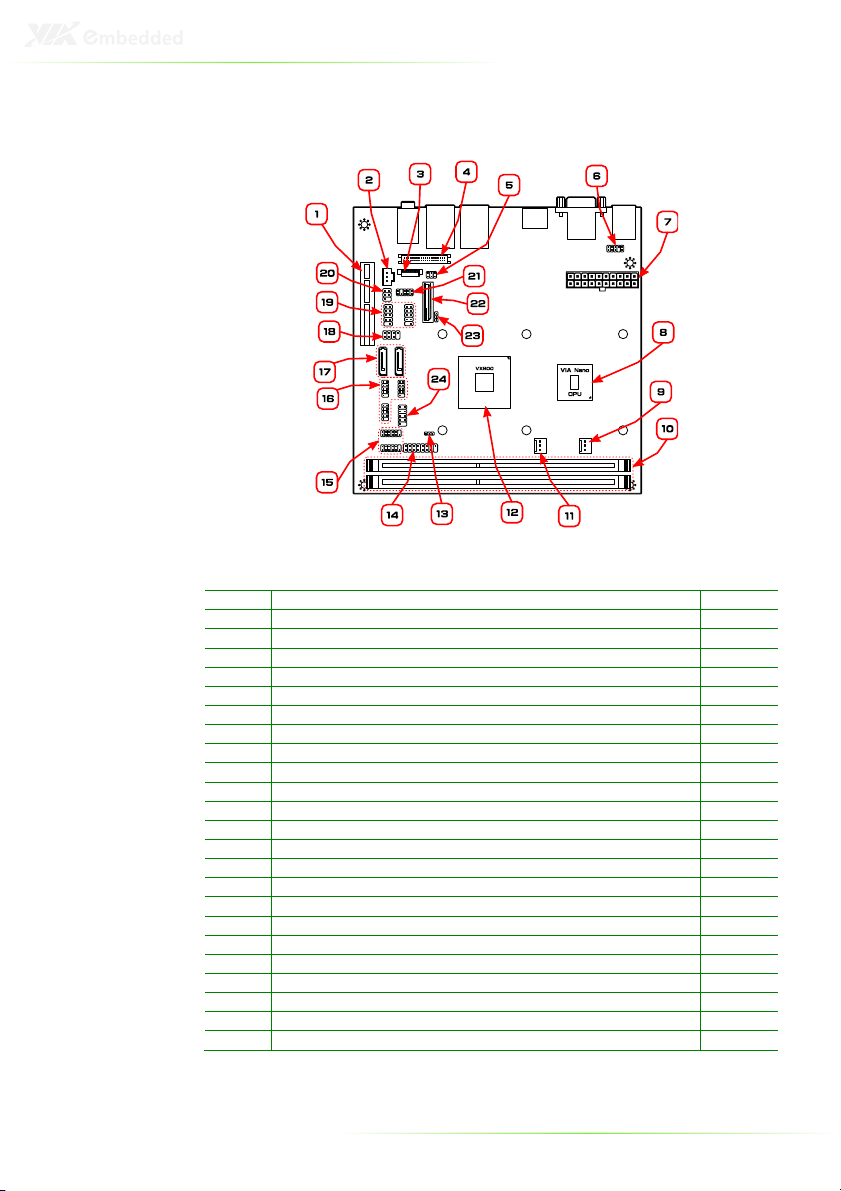
LAYOUT
Item Description Page
1 PCIE1: 1 x PCIe 4-lane slot 12
2 SPDIF1: SPDIF connector 17
3 BL1: Backlight inverter connector 11
4 LVDS1: LVDS connector 10
5 J3: LVDS power select and inverter select jumper 24
6 KBMS1: PS2 pin header for keyboard and mouse 17
7 CN1: 20-pin ATX connector 22
8 U16: VIA Nano CPU 2
9 FAN2: CPU fan 21
10 DIM1, DIM2: DDR3 slots 19
11 FAN1: System fan 21
12 U15: VIA VX900 2
13 SMB1: SMBus pin header 16
14 F_PANEL1: front panel pin header 18
15 DIO1, DIO2: Digital I/O pin headers 15
16 COM2, COM3, COM4: COM pin headers 14
17 SATA1, SATA2: SATA connectors 12
18 SPI1: SPI pin header 16
19 USB1_2, USB3_4: USB pin headers 13
20 USBD1: USB device port pin header 13
21 F_AUDIO1: front audio pin header 18
22 BAT1: CMOS battery socket 23
23 JBAT1: CMOS reset jumper 25
24 LPC1: LPC pin header 16
3
Page 11
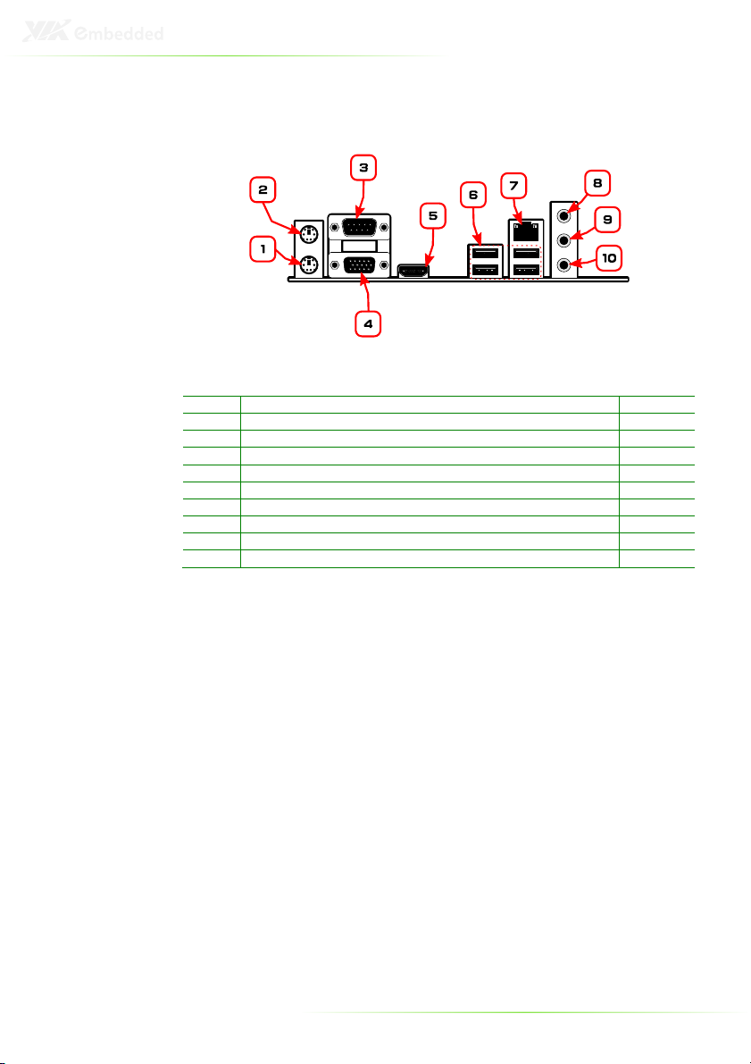
LAYOUT (I/O PANEL)
Item Description Page
1 PS/2 keyboard port 8
2 PS/2 mouse port 8
3 COM port 8
4 VGA port 8
5 HDMI® port 8
6 USB ports 8
7 GigaLAN port 8
8 Line-in 3.5 mm TRS jack 9
9 Line-out 3.5 mm TRS jack 9
10 MIC-in 3.5 mm TRS jack 9
4
Page 12

SPECIFICATIONS
Processor
Chipset
Super I/O
Memory
VGA
Storage
LAN
Audio
I/O
Expansion
Back Panel I/O
BIOS
Operating System
Fan
VIA 1.6 GHz Nano processor
Fanless
VIA 1.2GHz Nano processor
VIA VX900 Advanced all-in-one system processor
Fintek F81865-I
2 x DDR3 1066/800 MHz DIMM slot
(each slot can support a 4 GB module**)
Integrated VIA Chrome™ 9 HC3 3D/2D graphics
2 x SATA 3Gb/s connectors
VIA VT6130 PCIe Gigabit Ethernet controller
VIA VT1708S High Definition audio codec
2 x USB pin header (supports four USB ports)
1 x 2-channel 24-bit LVDS connector
1 x LVDS inverter connector
1 x front audio pin header
(Line-in/Mic-in or amplifier module)
1 x PS2 keyboard/mouse pin header
3 x RS232 pin header (configurable 5V/12V)
1 x LPC pin header
1 x SMBUS pin header
1 x S/PDIF Out connector
2 x Digital I/O pin header (GPI x 8, GPO x 8)
1 x front panel pin header
2 x Smart Fan connectors
1 x Temperature sensor on board
1 x ATX power connector
1 x 4-lane PCIe slot
2 x PS/2 connectors (mouse and keyboard)
1 x RS232 COM port
1 x VGA port
1 x RJ-45 LAN port
4 x USB ports
3 x Audio jacks (Line-out, Line-in, Mic-in)
AMI BIOS
4/8Mbit SPI Flash ROM
Windows 7, Windows CE, XPe, XP, Linux
5
Page 13
System Monitoring
Operating environment
Form Factor
Certifications
Compliance
Note:
*Specifications are subject to change without notice
**The actual Max memory capacity that could be recognized under a 64-bit OS will
be around 7.1GB due to the conflict in the memory space of the MMIO mapping.
- CPU voltage monitor
- System temperature monitor
- Wake-on-LAN, keyboard power-on, RTC timer,
Watch Dog timer
- System power management
- AC power failure recover
0°C ~ 60°C
0% ~ 95% (relative humidity; non-condensing)
Mini-ITX (17 cm x 17 cm)
CE/FCC, BSMI
RoHS
6
Page 14

2
Hardware
Installation
7
Page 15
EXTERNAL I/O
The external I/O panel has the following ports:
PS/2 ports
There are two PS/2 ports: one for a keyboard, one for a mouse.
VGA port
The 15-pin VGA port is for connecting to analog displays.
HDMI® port
The HDMI® port is for connecting to HDMI® displays.
COM ports
The 9-pin COM port is for pointing devices or other serial devices.
Gigabit LAN ports
The Gigabit Ethernet port is controlled through the VIA VT6130
PCIe Gigabit Ethernet controller.
USB ports
Four standard USB 2.0 ports are provided.
8
Page 16

Audio ports
Three 3.5 mm TRS jacks enable connections to Line-out, Line-in,
and Mic-in.
9
Page 17
ONBOARD CONNECTORS
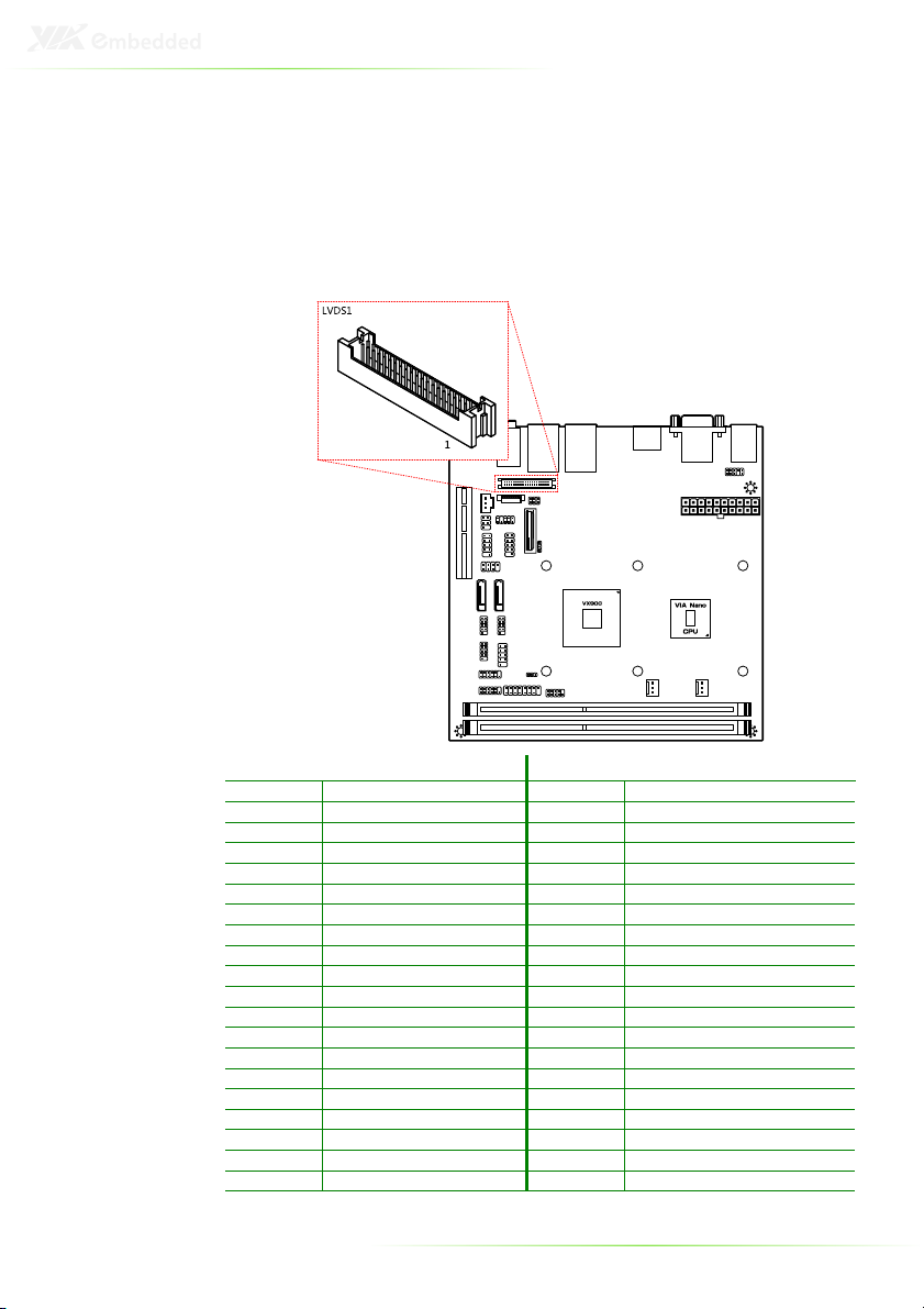
LVDS panel connector
The onboard LVDS panel connector LVDS1 supports dual-channel
24-bit displays.
Pin Signal Pin Signal
1 1LDC4- 2 PVDD1
3 1LDC4+ 4 PVDD1
5 GND 6 GND
7 1LDC5- 8 GND
9 1LDC5+ 10 1LDC011 GND 12 1LDC0+
13 1LDC6- 14 GND
15 1LDC6+ 16 1LDC117 GND 18 1LDC1+
19 1LCLK2- 20 GND
21 1LCLK2+ 22 1LDC223 GND 24 1LDC2+
25 1LDC7- 26 GND
27 1LDC7+ 28 1LCLK129 NC 30 1LCLK1+
31 GND 32 GND
33 NC 34 1LDC335 NC 36 1LDC3+
37 NC 38 LCD CLK
39 NC 40 LCD DATA
10
Page 18
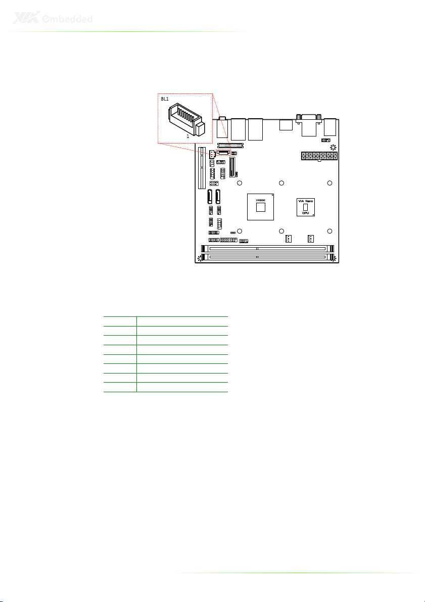
Inverter connector
The onboard inverter controls the LVDS panel backlight and
brightness.
Pin Signal
1 IVDD1_CEN
2 IVDD1_CEN
3 ENABLT/ENAVDD1
4 NC
5 ENAVDD1/ENABLT1
6 BRIGHTNESS1_CTL
7 GND
8 GND
11
Page 19

SATA connectors
There are two onboard SATA connectors that support data
transfer speeds up to 3 Gbps.
SATA1
Pin Signal Pin Signal
G1 G1 G1 G1
1 GND 1 GND
2 TX0+ 2 TX1+
3 TX0- 3 TX14 GND 4 GND
5 RX0- 5 RX16 RX0+ 6 RX1+
7 GND 7 GND
G2 G2 G2 G2
SATA2
PCIe slot
The onboard PCI Express slot supports one PCIe x4 expansion card.
12
Page 20

USB device port pin header
The onboard USB Device Port pin header can be configured to
support standard USB Client connectors through cabling and turn
the system into a device mode to be controlled by another PC or
smart device for transmitting data, synchronizing data, etc.
Pin Signal Pin Signal
1 +5VUSBD 2 USB_DP3 NC 4 USB_DP+
5 GND 6 —
Note:
USB Device port is a reserved
feature. Contact sales for
specific support.
USB pin header
The onboard USB pin headers enable the addition of four more
USB 2.0 ports.
USB1_2
Pin Signal Pin Signal
1 +5VDUAL 2 +5VDUAL
3 USBH_P1- 4 USBH_P75 USBH_P1+ 6 USBH_P7+
7 GND 8 GND
9 — 10 GND
USB3_4
Pin Signal Pin Signal
1 +5VDUAL 2 +5VDUAL
3 USBH_P2- 4 USBH_P65 USBH_P2+ 6 USBH_P6+
7 GND 8 GND
9 — 10 GND
13
Page 21

RS232 COM pin headers
The mainboard includes three COM pin headers onboard.
COM2
Pin Signal Pin Signal
1 -DCDA_2 2 RXDA_2
3 TXDA_2 4 -DTRA_2
5 GND 6 -DSRA_2
7 -RTSA_2 8 -CTSA_2
9 -RIA_2 10 —
COM3
Pin Signal Pin Signal
1 -DCDA_3 2 RXDA_3
3 TXDA_3 4 -DTRA_3
5 GND 6 -DSRA_3
7 -RTSA_3 8 -CTSA_3
9 -RIA_3 10 —
COM4
Pin Signal Pin Signal
1 -DCDA_4 2 RXDA_4
3 TXDA_4 4 -DTRA_4
5 GND 6 -DSRA_4
7 -RTSA_4 8 -CTSA_4
9 -RIA_4 10 —
14
Page 22

Digital I/O pin headers
The mainboard includes two Digital I/O pin headers that support
eight GPO and eight GPI pins.
DIO1
Pin Signal Pin Signal
1 DIO5V 2 DIO12V
3 GPO27 4 GPI19
5 GPO28 6 GPI20
7 GPO29 8 GPI21
9 GPO30 10 GPI22
11 GND 12 NC
DIO2
Pin Signal Pin Signal
1 DIO5V 2 DIO12V
3 GPO23 4 GPI15
5 GPO24 6 GPI16
7 GPO25 8 GPI17
9 GPO26 10 GPI18
11 GND 12 NC
15
Page 23

LPC pin header
The mainboard includes one LPC pin header.
Pin Signal Pin Signal
1 +3.3V 2 -LPCRST
3 LPCCLK1 4 LAD0
5 -LFRAME 6 LAD1
7 LAD3 8 LAD2
9 GND 10 —
SMBus pin header
The mainboard includes an SMBus pin header.
Pin Signal
1 SMBCK
2 SMBDT
3 GND
SPI pin header
The onboard SPI pin header provides support for one full-duplex
serial slave device.
Pin Signal Pin Signal
1 SPIVCC 2 GND
3 MSPISS0 4 MSPICLK
5 MSPIDI 6 MSPIDO
7 — 8 -PCIRST
16
Page 24

SPDIF connector
The mainboard includes one SPDIF connector.
Pin Signal
1 +5VAUDIO
2 SPDIFO
3 GND
PS/2 keyboard and mouse pin header
The mainboard includes one pin header for adding support for
PS/2 keyboard and mouse.
Pin Signal Pin Signal
1 +5VDUAL 2 +5VDUAL
3 NC 4 —
5 GND 6 GND
7 KB_DT 8 MS_DT
9 KB_CK 10 MS_CK
17
Page 25

Front audio pin header
The mainboard has one pin header for connecting to front audio
Headphone-out and Mic-in jacks.
Pin Signal Pin Signal
1 LINE2R 2 LINE2L
3 NC 4 NC
5 MIC2_IN_R 6 MIC2_IN_L
7 — 8 NC
9 GND 10 GND
Front panel pin header
The mainboard has one pin header for connecting to front panel
switches and status LEDs.
Pin Signal Pin Signal
1 +5VDUAL 2 +5V
3 +5VDUAL 4 HD_LED
5 PW_LED 6 PWR_BTN
7 +5V 8 GND
9 NC 10 -RST_SW/-SUSB
11 NC 12 GND
13 SPEAK_BZ 14 +5V
15 — 16 NC
18
Page 26

Memory module slots
The mainboard includes two DIMM memory module slots that
support DDR3 memory.
19
Page 27

To install the memory modules:
1. Disengage the locking mechanism at both ends of the
DIMM slot.
2. Align the notch at the bottom of the DIMM with the
counterpart on the DIMM slot.
3. Then insert the DIMM into the slot and push down at
both ends until the locking clips snap into position.
20
Page 28

CPU fan and system fan connectors
FAN1 (system) and FAN2 (CPU) run on +12V and maintains
system cooling. When connecting the cable to the connector,
always be aware that the red wire (positive wire) should be
connected to the pin 1. The black wire is the ground wire and
should always be connected to GND.
FAN1
Pin Signal Pin Signal
1 FAN_IN1 1 FAN_IN2
2 FAN_CTL1 2 FAN_CTL2
3 GND 3 GND
FAN2
21
Page 29

ATX power connector
The mainboard supports a conventional ATX power supply for the
power system. Before inserting the power supply connector,
always make sure that all components are installed correctly to
ensure that no damage will be caused. To connect the power
supply, make sure the power plug is inserted in the proper
orientation and the pins are aligned. Then push down the plug
firmly into the connector.
Pin Signal Pin Signal
1 +3.3V 2 +3.3V
3 +3.3V 4 -12V
5 GND 6 GND
7 +5V 8 PS_ON
9 GND 10 GND
11 +5V 12 GND
13 GND 14 GND
15 PW_OK 16 -5V
17 +5V_SB 18 +5V
19 +12V 20 +5V
22
Page 30

CMOS battery
The onboard battery provides power to the CMOS RAM. If
disconnected all configurations in the CMOS RAM will be reset to
factory defaults. When replacing the battery, use CR2032 coin
batteries.
23
Page 31

ONBOARD JUMPERS
LVDS jumper settings
The LVDS connectors and LVDS inverters can operate on different
input voltages. Pins 1, 3, and 5 correspond to BL1. Pins 2, 4, and 6
correspond to LVDS1.
BL1 power 1 3 5
+12V ON ON OFF
+5V (default) OFF ON ON
LVDS1 power 2 4 6
+3.3V ON ON OFF
+5V (default) OFF ON ON
24
Page 32

Clear CMOS jumper
The onboard CMOS RAM stores system configuration data and
has an onboard battery power supply. To reset the CMOS settings,
set the jumper on pins 2 and 3 while the system is off. Return the
jumper to pins 1 and 2 afterwards. Setting the jumper while the
system is on will damage the mainboard. The default setting is on
pins 1 and 2.
Setting 1 2 3
Normal Operation (default) ON ON OFF
Clear CMOS setting OFF ON ON
Caution:
Except when clearing the RTC RAM, never remove the cap from the CLEAR_CMOS
jumper default position. Removing the cap will cause system boot failure. Avoid
clearing the CMOS while the system is on; it will damage the mainboard.
25
Page 33

3
BIOS Setup
26
Page 34

ENTERING THE BIOS SETUP MENU
Power on the computer and press <Delete> during the beginning
of the boot sequence to enter the BIOS setup menu. If you missed
the BIOS setup entry point, restart the system and try again.
CONTROL KEYS
Keys Description
Up Move to the previous item
Down Move to the next item
Left Move to the previous tab
Right Move to the next tab
Enter Select the item
Esc Jumps to the Exit menu or returns to the main menu
+ (number pad) Increase the numeric value
- (number pad) Decrease the numeric value
F1 General help, only for Status Page Setup Menu and
F7 Discard Changes
F9 Load Optimized defaults
F10 Save all the changes and exit
from a submenu
Option Page Setup Menu
27
Page 35

GETTING HELP
The BIOS setup program provides a “General Help” screen. You
can display this screen from any menu/sub-menu by pressing
<F1>. The help screen displays the keys for using and navigating
the BIOS setup. Press <Esc> to exit the help screen.
28
Page 36

MAIN MENU
AMIBIOS
BIOS version number and related information.
Processor
This section describes the detected CPU name, speed, and
number of processors.
System Memory
This section describes the detected memory size.
System Time
Use the key “+” or “-” to configure system time. The time format is
[Hour : Minute : Second].
System Date
Use the key “+” or “-” to configure system Date. The date format is
[Day, Month, Date, Year].
29
Page 37

ADVANCED SETTINGS
Available submenus include the following:
• CPU Configuration
• IDE Configuration
• SuperIO Configuration
• Hardware Health Configuration
• WatchDog Configuration
• ACPI Configuration
• APM Configuration
• USB Configuration
• CRB Configuration
30
Page 38

CPU CONFIGURATION
CPU Thermal Control
This option is used to enable the internal thermal protection
features inside the onboard Nano CPU.
Settings Description
Disabled No thermal monitoring
TM3 Enables Thermal Monitor 3
31
Page 39

IDE CONFIGURATION
Available submenus include the following:
• Primary IDE Master
• Primary IDE Slave
32
Page 40

IDE DRIVES
PIO Mode
The Programmed Input/Output mode is a data transfer method
that uses the CPU registers to transfer data.
Settings Description
Auto The Programmed Input/Output mode is automatically selected.
0 Maximum transfer rate of 3.3 MB/s. Cycle time: 600ns. Defined
in ATA specification.
1 Maximum transfer rate of 5.2 MB/s. Cycle time: 383ns. Defined
in ATA specification.
2 Maximum transfer rate of 8.3 MB/s. Cycle time: 240ns. Defined
in ATA specification.
3 Maximum transfer rate of 11.1 MB/s. Cycle time: 180ns. Defined
in ATA-2 specification.
4 Maximum transfer rate of 16.7 MB/s. Cycle time: 120ns. Defined
in ATA-2 specification.
DMA Mode
The Direct Memory Access mode is a data transfer method that
bypasses the CPU and directly transfers between the system
memory and the connected IDE device.
Settings Description
Auto The Direct Memory Access mode is automatically selected.
33
Page 41

SUPERIO CONFIGURATION
Serial Port Address, IRQ, and Type
The SuperIO configuration menu enables the BIOS to specifically
define the resources used for serial ports 1 – 4.
Port Address IRQ
1 3F8, 3E8, 2E8,
Disabled
2 2F8, 3E8, 2E8,
Disabled
3 3F8, 2F8, 3E8,
2E8, 2D0, 2E0,
Disabled
4 3F8, 2F8, 3E8,
2E8, 2D0, 2E0,
Disabled
3, 4, 10, 11
3, 4, 10, 11
3, 4, 10, 11
3, 4, 10, 11
34
Page 42

HARDWARE HEALTH CONFIGURATION
The Hardware Health Configuration displays all monitored
information. System Temperature is taken from a sensor (PHILIPS
PMBT3904 SOT-23).
H/W Health Function
Settings Description
Disabled Support for this feature will be unavailable.
Enabled Enables the Hardware Health Monitoring device.
35
Page 43

WATCHDOG CONFIGURATION
The WatchDog function monitors the system to ensure that the
system has not frozen. If the system appears to have frozen for a
specific period of time, then the WatchDog function will force the
system to reboot.
WatchDog Control
Settings Description
Disabled Disables the WatchDog function
Enabled Will monitor the system.
Time
This option is only visible when the WatchDog function is enabled.
Settings Description
0 ~ 255 Any integer in the range of 0 to 255.
Unit
This option is only visible when the WatchDog function is enabled.
Settings Description
Second Sets the time unit to seconds.
Minute Sets the time unit to minutes.
36
Page 44

ACPI CONFIGURATION
Suspend Mode
Select the ACPI state used for system suspend.
Settings Description
S1(POS) S1/Power On Suspend (POS) is a low power state. In this
state, no system context (CPU or chipset) is lost and
hardware maintains all system contexts
S3(STR) S3/Suspend To RAM (STR) is a power-down state. In this
state, power is supplied only to essential components
such as main memory and wakeup-capable devices. The
system context is saved to main memory, and context is
restored from the memory when a "wakeup" event
occurs.
Auto Depends on the OS to select the state.
ACPI Version Features
To enable RSDP pointers to 64-bit Fixed System Description Tables.
Settings Description
ACPI v1.0 Supports ACPI v1.0
ACPI v2.0 Supports ACPI v2.0
ACPI v3.0 Supports ACPI v3.0
37
Page 45

APM CONFIGURATION
Power Button Mode
Settings Description
On/Off Pressing the power button will Instantly cause the system to
power on or off.
Standby Requires the user to press and hold the power button for 4
seconds before powering off the system.
Suspend Pressing the power button will Instantly cause the system to
enter suspend mode.
Restore on AC / Power Loss
The field defines how the system will respond after an AC power
loss during system operation.
Settings Description
Power Off Keeps the system in an off state until the power button is
Power On Restarts the system when the power is back
Last State Save in last state
pressed.
Resume on PCI Express
Settings Description
Enabled The system will boot if any power management event is
Disabled The feature will be disabled.
triggered via PCI Express devices
38
Page 46

Resume On PS/2 KBC
Enables any detected keyboard activity to restore the system from
a power saving mode to an active state.
Settings Description
S3 PS/2 keyboard activity will be detected if the system is in
S3/S4/S5 PS/2 keyboard activity will be detected if the system is in
Disabled Disables the detection of PS/2 keyboard activity.
S3 power saving mode.
S3/S4/S5 power saving mode.
Wake-Up Key
This option can only be modified when Resume on PS/2 KBC is
enabled.
Settings Description
Any Key Any key can be used to wake up the system.
Specific Key This option unlocks the Wake-Up Password option.
Wake-Up Password
This option can only be modified when Wake-Up Key is set to
Specific Key. When selected, a prompt will be displayed requesting
a password for waking up the system. This password can consist
of up to 6 alphanumeric characters and some special characters.
Function keys and modifier keys (such as Ctrl, Alt, Del, etc.) cannot
be used.
Resume on PS/2 Mouse
Enable any PS/2 mouse activity to restore the system from the
power saving mode to an active state.
Settings Description
S3 PS/2 mouse activity will be detected if the system is in S3
S3/S4/S5 PS/2 mouse activity will be detected if the system is in
Disabled Disables the detection of PS/2 mouse activity.
power saving mode.
S3/S4/S5 power saving mode.
Resume on RTC Alarm
This feature enables the BIOS to automatically power on at a
scheduled time.
Settings Description
Enabled Unlocks the RTC Alarm Date and System Time options.
Disabled Support for this feature will be unavailable.
39
Page 47

RTC Alarm Date (Days)
This option enables the user to specify the frequency of the RTC
Alarm Date recurrence.
Settings Description
Every Day Triggers the RTC Alarm Date daily.
1 – 31 (days) Triggers the RTC Alarm Date according to the increment
specified.
System Time
This option enables the user to specify the power on time for the
scheduled recurring date.
40
Page 48

USB CONFIGURATION
The USB configuration page detects all connected USB devices.
41
Page 49

CRB CONFIGURATION
DRAM Clock
Settings Description
Auto Auto adjusts the DRAM clock
400 MHz Sets the DRAM clock to 400 MHz. DDR3 modules will
operate at 800 MHz.
533 MHz Sets the DRAM clock to 533 MHz. DDR3 modules will
operate at 1066 MHz.
Select Display Device 1 and 2
The system can output data to two display devices simultaneously.
Settings Description
CRT1 Specifies the CRT1 port as the display port being used.
LCD2 Specifies the LCD2 port as the display port being used.
LCD1 Specifies the LCD1 port as the display port being used.
HDMI® Specifies the HDMI® port as the display port being used.
DP Specifies the DP port as the display port being used.
42
Page 50

Panel Type and Panel Type 2
This feature enables the user to specify the resolution of the display
being used with the system. The panel types are predefined in the
VGA VBIOS.
Settings Description
00 640 x 480
01 800 x 600
02 1024 x 768
03 1280 x 768
04 1280 x 1024
05 1400 x 1050
06 1440 x 900
07 1280 x 800
08 800 x 480
09 1024 x 600
10 1366 x 768
11 1600 x 1200
12 1680 x 1050
13 1920 x 1200
14 1920 x 1080
15 1024 x 576
VGA Share Memory (Frame Buffer)
Settings Description
8MB Allocates 8 MB of system DRAM for the VGA frame buffer.
16MB Allocates 16 MB of system DRAM for the VGA frame buffer.
32MB Allocates 32 MB of system DRAM for the VGA frame buffer.
64MB Allocates 64 MB of system DRAM for the VGA frame buffer.
128MB Allocates 128 MB of system DRAM for the VGA frame buffer.
256MB Allocates 256 MB of system DRAM for the VGA frame buffer.
512MB Allocates 512 MB of system DRAM for the VGA frame buffer.
Backlight Control
This option sets the brightness control for an LCD device.
Settings Description
0% Sets the panel backlight brightness to 0%.
25% Sets the panel backlight brightness to 25%.
50% Sets the panel backlight brightness to 50%.
75% Sets the panel backlight brightness to 75%.
100% Sets the panel backlight brightness to 100%.
OnChip HDAC Device
Settings Description
Enabled Enables the HD audio codec in the VT1708S controller.
Disabled Disables the HD audio codec in the VT1708S controller.
43
Page 51

VT6130 LAN Control 1
Settings Description
Enabled Enable the onboard PCIe GigaLAN controller.
Disabled Disables the onboard PCIe GigaLAN controller and hides
it from the operating system.
LAN Boot ROM
This option enables the PXE feature for booting via LAN.
Settings Description
Enabled Enables the PXE feature of the LAN controller.
Disabled Does not load a separate ROM from the LAN controller.
44
Page 52

BOOT SETTINGS
The Boot Settings menu has the following submenu:
Boot Settings Configuration
Configuration settings during system boot.
45
Page 53

BOOT SETTINGS CONFIGURATION
Quick Boot
Settings Description
Enabled Enables the BIOS to skip certain tests in order to reduce
boot up time.
Disabled Support for this feature will be unavailable.
Quiet Boot
Settings Description
Enabled Displays an OEM logo instead of POST messages.
Disabled Displays POST messages.
Bootup Num-Lock
Settings Description
On For keyboards with a built-in 10-key pad, the BIOS will
Off For keyboards with a built-in 10-key pad, the keypad will
force the keypad to behave in 10-key mode.
behave as a cursor keypad.
Wait For ‘F1’ If Error
Settings Description
Enabled If an error is detected, the BIOS will pause booting and
Disabled Ignores errors while booting.
wait for the user to press F1 to enter the BIOS setup
menu.
46
Page 54

Hit ‘DEL’ Message Display
Settings Description
Enabled Shows the POST message that informs the user how to
Disabled Hides the POST message that informs the user how to
enter the BIOS setup menu. However, this message will
be hidden if the Display Logo option is enabled.
enter the BIOS setup menu.
47
Page 55

SECURITY SETTINGS
Change Supervisor Password
This option is for setting a password for accessing the BIOS setup
utility. When a password has been set, a password prompt will be
displayed whenever the BIOS setup utility is launched. This
prevents an unauthorized person from changing any part of the
system configuration.
When a supervisor password is set, the User Access Level and
Password Check options will be unlocked.
User Access Level
This feature controls the level of access a user (without the
supervisor password) is granted to the BIOS setup utility.
Settings Description
No Access Completely locks the BIOS setup utility. The supervisor
View Only Only allows access to view the BIOS settings.
Limited Only allows non-critical BIOS settings to be changed.
Full Access Allows all BIOS settings to be changed except for the
password is required to access and change the BIOS
settings..
Changes are allowed to the following options:
System Time
System Date
Quick Boot
Display Logo
Change Supervisor Password and User Access Level
options.
48
Page 56

Change User Password
This option is for setting a password for non-supervisors. When a
user password is set, the Clear User Password and Password
Check options will be unlocked.
Clear User Password
This option is only available when the user accesses the BIOS
Setup Utility when the user password has been specified.
Password Check
This feature is compulsory when the Change Supervisor Password
option is set. The user will have up to three chances to enter the
correct password before the BIOS forces the system to stop
booting. If the user does not enter the correct password, the
keyboard will also lock up. The only way to get past this is to do a
hard reboot (i.e., use the system reset button or cut off the power
to the system). A soft reboot (i.e., Ctrl+Alt+Del) will not work
because the keyboard will be locked.
Settings Description
Setup Force users to enter a password in order to access the
Always Force users to enter a password in order to boot up the
BIOS setup utility.
system.
49
Page 57

EXIT OPTIONS
Save Changes and Exit
Save all changes to the BIOS and exit the BIOS Setup Utility. The
“F10” hotkey can also be used to trigger this command.
Discard Changes and Exit
Exit the BIOS Setup Utility without saving any changes. The “Esc”
hotkey can also be used to trigger this command.
Discard Changes
This command reverts all changes to the settings that were in
place when the BIOS Setup Utility was launched. The “F7” hotkey
can also be used to trigger this command.
Load Optimal Defaults
Load optimal default values for all the setup items. The default
optimized values are defined by the mainboard manufacturer to
provide optimized environment for a basic system. The “F9” hotkey
can also be used to trigger this command.
50
Page 58

4
Driver Installation
51
Page 59

MICROSOFT DRIVER SUPPORT
The VIA EPIA-M850 mainboard is compatible with Microsoft
operating systems. The latest Windows drivers can be
downloaded from the VIA Embedded website at
www.viaembedded.com.
For embedded operating systems, the related drivers can be
found in the VIA Embedded website at
www.viaembedded.com.
LINUX DRIVER SUPPORT
The VIA EPIA- M850 mainboard is highly compatible with many
Linux distributions.
Support and drivers are provided through various methods
including:
1. Drivers provided by VIA
2. Using a driver built into a distribution package
3. Visiting www.viaembedded.com for the latest updated
drivers
4. Installing a third party driver (such as the ALSA driver from
the Advanced Linux Sound Architecture project for
integrated audio)
For OEM clients and system integrators developing a product for
long term production, other code and resources may also be
made available. Contact VIA Embedded to submit a request.
52
Page 60

Taiwan Headquarters USA Europe
1F, 531 Zhong-Zheng Road
Xindian District, New Taipei City 231,
Taiwan
TEL: 886.2.2218.5452
FAX: 886.2.2218.5453
Email: embedded@via.com.tw
940 Mission Court
Fremont, CA 94539
USA
TEL: 1.510.683.3300
FAX: 1.510.687.4654
Email: embedded@viatech.com
In den Dauen 6
53117 Bonn
Germany
TEL: 49.228.688565.0
FAX: 49.228.688565.19
Email: embedded@via-tech.de
China Japan Korea
Tsinghua Science Park Bldg. 7
No. 1 Zongguancun East Road
Haiden District, Beijing, 100084
China
TEL: 86.10.59852288
FAX: 86.10.59852299
Email: embedded@viatech.com.cn
3-15-7 Ebisu MT Bldg. 6F
Higashi, Shibuya-ku
Tokyo 150-0011
Japan
TEL: 81.3.5466.1637
FAX: 81.3.5466.1638
Email: embedded@viatech.co.jp
2F, Sangjin Bldg., 417
Dogok Dong, Gangnam-Gu
Seoul 135-854
South Korea
TEL: 82.2.571.2986
FAX: 82.2.571.2987
Email: embedded@via-korea.com
 Loading...