

Page 1

Revision
1.06
user manual
EPIA-M840
Mini-ITX Embedded Board
Page 2
Copyright
Copyright © 2010 VIA Technologies Incorporated. All rights reserved.
No part of this document may be reproduced, transmitted, transcribed, stored in a
retrieval system, or translated into any language, in any form or by any means, electronic,
mechanical, magnetic, optical, chemical, manual or otherwise without the prior written
permission of VIA Technologies, Incorporated.
Trademarks
All trademarks are the property of their respective holders.
PS/2 is a registered trademark of IBM Corporation.
Disclaimer
No license is granted, implied or otherwise, under any patent or patent rights of VIA
Technologies. VIA Technologies makes no warranties, implied or otherwise, in regard to
this document and to the products described in this document. The information provided
in this document is believed to be accurate and reliable as of the publication date of this
document. However, VIA Technologies assumes no responsibility for the use or misuse of
the information in this document and for any patent infringements that may arise from the
use of this document. The information and product specifications within this document are
subject to change at any time, without notice and without obligation to notify any person
of such change.
VIA Technologies, Inc. reserves the right the make changes to the products described in
this manual at any time without prior notice.
Regulatory Compliance
FCC-A Radio Frequency Interference Statement
This equipment has been tested and found to comply with the limits for a class A digital
device, pursuant to part 15 of the FCC rules. These limits are designed to provide
reasonable protection against harmful interference when the equipment is operated in a
commercial environment. This equipment generates, uses, and can radiate radio
frequency energy and, if not installed and used in accordance with the instruction manual,
may cause harmful interference to radio communications. Operation of this equipment in a
residential area is likely to cause harmful interference, in which case the user will be
required to correct the interference at his personal expense.
Notice 1
The changes or modifications not expressly approved by the party responsible for
compliance could void the user's authority to operate the equipment.
Notice 2
Shielded interface cables and A.C. power cord, if any, must be used in order to comply
with the emission limits.
Tested To Comply
With FCC Standards
FOR HOME OR OFFICE USE
Battery Recycling and Disposal
Only use the appropriate battery specified for this product.
Do not re-use, recharge, or reheat an old battery.
Do not attempt to force open the battery.
Do not discard used batteries with regular trash.
Discard used batteries according to local regulations.
II
Page 3

Safety Precautions
Do’s
o Always read the safety instructions carefully.
o Keep this User's Manual for future reference.
o All cautions and warnings on the equipment should be
noted.
o Keep this equipment away from humidity.
o Lay this equipment on a reliable flat surface before setting
it up.
o Make sure the voltage of the power source and adjust
properly 110/220V before connecting the equipment to the
power inlet.
o Place the power cord in such a way that people cannot
step on it.
o Always unplug the power cord before inserting any add-on
card or module.
o If any of the following situations arises, get the equipment
checked by authorized service personnel:
o The power cord or plug is damaged.
o Liquid has penetrated into the equipment.
o The equipment has been exposed to moisture.
o The equipment has not worked well or you cannot
get it work according to User's Manual.
o The equipment has dropped and damaged.
o The equipment has obvious sign of breakage.
Don’ts
o Do not leave this equipment in an environment
unconditioned or in a storage temperature above 60°C
(140°F). The equipment may be damaged.
o Do not leave this equipment in direct sunlight.
o Never pour any liquid into the opening. Liquid can cause
damage or electrical shock.
o Do not place anything over the power cord.
o Do not cover the ventilation holes. The openings on the
enclosure protect the equipment from overheating
III
Page 4

IV
Box Contents and Ordering Information
Model Number Description
EPIA-M840-16 Standard kit
EPIA-M840-12 Standard kit
1 x SATA cable
1 x I/O bracket
1 x Driver CD
1 x SATA cable
1 x I/O bracket
1 x Driver CD
Page 5

V
T
ABLE OF
C
ONTENTS
1 Overview .................................................................................................................1
Key Components ................................................................................................. 2
VIA Nano™ NanoBGA2 CPU ..................................................................2
VIA VX800 System Processor ................................................................... 2
Layout (top view) ................................................................................................ 3
Layout (I/O panel)...............................................................................................5
Specifications ......................................................................................................... 6
2 Hardware Installation........................................................................................ 8
External I/O ............................................................................................................9
PS/2 ports........................................................................................................... 9
VGA port ............................................................................................................9
COM ports ......................................................................................................... 9
Gigabit LAN ports ..........................................................................................9
USB ports............................................................................................................ 9
Audio ports........................................................................................................ 9
Onboard connectors.......................................................................................10
LVDS panel connectors ............................................................................10
Inverter connectors .....................................................................................12
SATA connectors..........................................................................................13
SATA power connectors ..........................................................................14
IDE connector................................................................................................15
Compact Flash slot ......................................................................................16
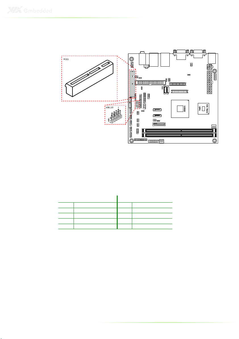
PCIe slot.............................................................................................................17
USB pin header .............................................................................................17
RS232 COM pin headers..........................................................................18
Digital I/O pin headers..............................................................................19
LPT pin header...............................................................................................20
LPC pin header..............................................................................................21
FIR pin header................................................................................................22
SMBus pin header........................................................................................22
MFX pin header ............................................................................................23
SPI pin header................................................................................................23
SPDIF connector...........................................................................................24
PS/2 keyboard and mouse pin header .............................................24
Front audio pin header.............................................................................25
Front panel pin header .............................................................................25
Page 6

Memory module slots ................................................................................26
CPU fan and system fan connectors ..................................................28
Thermal sensor pin header .....................................................................28
ATX power connector...............................................................................29
DC-in power connector............................................................................30
CMOS battery.................................................................................................30
Onboard Jumpers ............................................................................................31
LVDS jumper settings.................................................................................31
LVDS2 jumper settings ..............................................................................31
SATA DOM power select .........................................................................32
CF power select ............................................................................................32
IDE DOM power select .............................................................................33
COM power select.......................................................................................33
Clear CMOS jumper....................................................................................34
AT/ATX mode jumper ...............................................................................35
3 BIOS Setup............................................................................................................36
Entering the BIOS Setup Menu ..................................................................37
Control Keys .........................................................................................................37
Getting Help ........................................................................................................38
Main Menu ...........................................................................................................39
Standard CMOS Features.........................................................................39
Advanced BIOS Features .........................................................................39
Advanced Chipset Features....................................................................39
Integrated Peripherals................................................................................39
Power Management Setup.....................................................................39
PnP/PCI Configurations.............................................................................39
PC Health Status............................................................................................40
Frequency/Voltage Control....................................................................40
Load Optimized Defaults..........................................................................40
Set Supervisor Password ...........................................................................40
Set User Password .......................................................................................40
Save & Exit Setup ..........................................................................................40
Exit Without Saving.....................................................................................40
Standard CMOS Features..............................................................................41
Date ....................................................................................................................41
Time ....................................................................................................................41
Video..................................................................................................................41
Halt On..............................................................................................................41
HDD Channels ...................................................................................................42
Advanced BIOS Features...............................................................................43
Virus Warning................................................................................................43
CPU L1 & L2 Cache.....................................................................................43
CPU L2 Cache ECC Checking................................................................43
Quick Power On Self-Test.........................................................................44
VI
Page 7

First/Second/Third Boot Device............................................................44
Boot Other Device.......................................................................................44
Boot Up NumLock Status.........................................................................44
Typematic Rate Setting ..............................................................................44
Typematic Rate (Chars/Sec) ....................................................................45
Typematic Delay (Msec)............................................................................45
Security Option..............................................................................................45
MPS Version Control for OS....................................................................45
OS Select for DRAM > 64MB ..................................................................45
HDD S.M.A.R.T Capability .........................................................................45
Video BIOS Shadow ...................................................................................45
Full Screen Logo Show .............................................................................46
Summary Screen Show.............................................................................46
CPU Features.......................................................................................................47
Thermal Management...............................................................................47
Hard Disk Boot Priority....................................................................................48
Advanced Chipset Features .........................................................................49
Memory Hole .................................................................................................49
System BIOS Cacheable ............................................................................49
Video RAM Cacheable ..............................................................................49
Internal VGA Control.......................................................................................50
VGA Share Memory Size ..........................................................................50
Direct Frame Buffer.....................................................................................50
Select Display Device..................................................................................50
Panel Type .......................................................................................................51
CPU & PCI Bus Control ...................................................................................52
PCI Master 0 WS Write ..............................................................................52
PCI Delay Transaction ................................................................................52
Integrated Peripherals.....................................................................................53
Onboard LAN Boot ROM ........................................................................53
VIA OnChip IDE Device .................................................................................54
CF Card UDMA66 .......................................................................................54
SATA Controller.............................................................................................54
IDE DMA Transfer Access ........................................................................54
OnChip IDE Channel 1 .............................................................................54
IDE Prefetch Mode ......................................................................................54
Secondary Master PIO ...............................................................................54
Secondary Slave PIO...................................................................................54
Secondary Master UDMA ........................................................................54
Secondary Slave UDMA............................................................................55
IDE HDD Block Mode ................................................................................55
VIA OnChip PCI Device..................................................................................56
Azalia HDA Controller................................................................................56
SuperIO Device...................................................................................................57
VII
Page 8

Serial ports........................................................................................................57
Onboard Parallel Port.................................................................................57
Parallel Port Mode........................................................................................58
ECP Mode Use DMA ..................................................................................58
Internal IrDA Controller.............................................................................58
IR IRQ..................................................................................................................58
IR DMA ..............................................................................................................58
USB Device Setting ...........................................................................................59
USB 1.0 Controller .......................................................................................59
USB 2.0 Controller .......................................................................................59
USB Operation Mode ................................................................................59
USB Keyboard Function............................................................................59
USB Mouse Function .................................................................................59
USB Storage Function................................................................................60
Power Management Setup..........................................................................61
ACPI Suspend Type .....................................................................................61
Power Management Option..................................................................61
HDD Power Down .....................................................................................62
Suspend Mode ..............................................................................................62
Video Off Option..........................................................................................62
Video Off Method........................................................................................62
MODEM Use IRQ .........................................................................................62
Soft-Off by PWRBTN....................................................................................62
Run VGABIOS if S3 Resume....................................................................63
AC Loss Auto Restart ..................................................................................63
WatchDog Run/Stop .................................................................................63
WatchDog Count Value ..........................................................................63
Wakeup Event Detect.....................................................................................64
PS2KB Wakeup Select ................................................................................64
PS2KB Wakeup Key Select .......................................................................64
PS2MS Wakeup Key Select ......................................................................64
PS2 Keyboard Power ON.........................................................................64
PS2 Mouse Power ON...............................................................................64
RTC Alarm Resume ......................................................................................65
Date (of Month)............................................................................................65
Resume Time (hh : mm : ss) ....................................................................65
PnP/PCI Configurations..................................................................................66
Init Display First..............................................................................................66
PNP OS Installed ...........................................................................................66
Reset Configuration Data.........................................................................66
Resources Controlled By...........................................................................67
PCI/VGA Palette Snoop ............................................................................67
Assign IRQ for VGA.....................................................................................67
Assign IRQ for USB ......................................................................................67
VIII
Page 9

Maximum Payload Size..............................................................................67
IRQ Resources .....................................................................................................68
PC Health Status.................................................................................................69
Frequency/Voltage Control.........................................................................70
DRAM Frequency ........................................................................................70
DDR CAS Latency Control .......................................................................70
DDR Burst Length........................................................................................70
DDR 1T Command Rate ...........................................................................70
DRDY Table .....................................................................................................70
ODT.....................................................................................................................70
Spread Spectrum..........................................................................................71
Load Optimized Defaults...............................................................................72
Set Supervisor/User Password ....................................................................73
Save & Exit Setup ...............................................................................................74
Exit Without Saving ..........................................................................................75
IX
Page 10

1
Overview
1
Page 11

The VIA EPIA-M840 Mini-ITX Mainboard is a compact native x86
mainboard optimized for entry level systems in embedded and
productivity applications. It provides support for high fidelity audio
with its onboard VIA VT1708S High Definition Audio codec. In
addition it supports two SATA 3Gb/s storage devices as well as
IDE.
The EPIA-M840 is based on the VIA VX800 Unified Digital Media
IGP chipset featuring the VIA Chrome9™ HC3 with 2D/3D
graphics and video accelerators for rich digital media performance.
KEY COMPONENTS
VIA Nano™ NanoBGA2 CPU
The VIA Nano is a 64-bit superscalar processor in x86 platform
using a 65 nanometer process technology. It delivers an energyefficient, powerful performance, with cool and quiet operation all
within an ultra compact NanoBGA2 package measuring 21mm x
21mm. Perfectly fit for embedded system applications such as
industrial PCs, test machines, measuring equipment, digital
signage, medical PCs, monitoring systems, gaming machines, invehicle entertainment, and etc. The VIA Nano also boasts of
immersive multimedia performance, connectivity and computing
applications.
VIA VX800 System Processor
The VIA VX800 media system processor is an all-in-one, highly
integrated digital media IGP chipset featuring the latest video,
graphics and connectivity performance in a single chip measuring
just 33x33mm.
2
Page 12
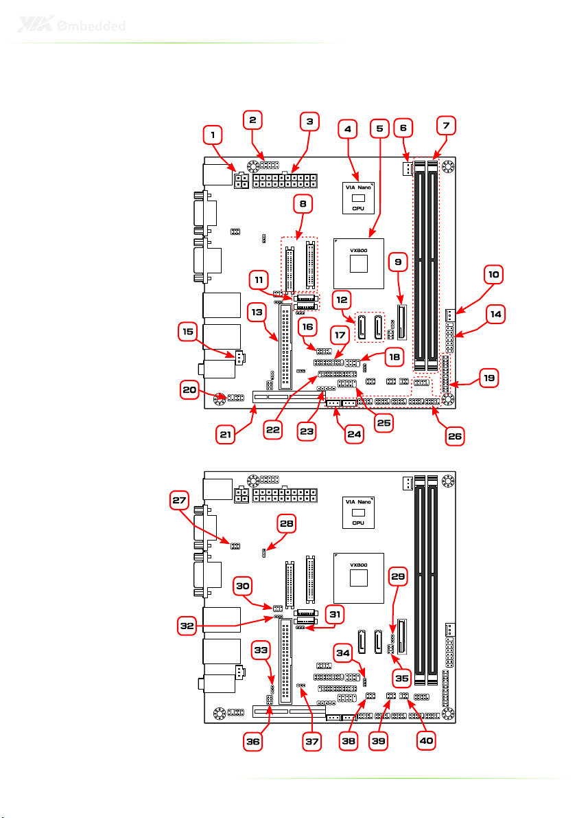
LAYOUT (TOP VIEW)
3
Page 13
Item Description Page
1 DC-in power connector (DC12V1) 30
2 PS/2 keyboard and mouse pin header (KBMS) 24
3 ATX power supply connector (ATX_POWER1) 29
4 VIA Nano CPU (U16) 2
5 VIA VX800 chipset (U15) 2
6 CPU fan connector (CPUFAN1) 28
7 Memory slots (DIMM1, DIMM2) 26
8 LVDS connectors (LVDS1, LVDS2) 10
9 CMOS battery socket (BAT1) 30
10 System fan connector (SYSFAN1) 28
11 LVDS inverter connectors (INVERTER1, INVERTER2) 12
12 SATA connectors (SATA1, SATA2) 13
13 IDE connector (IDE1) 15
14 Front panel pin header (F_PANEL1) 25
15 SPDIF connector (SPDIF1) 24
16 MFX pin header (MFX1) 23
17 LPC pin header (LPC1) 21
18 SPI pin header (SPI1) 23
19 Digital I/O pin headers (DIO1, DIO2) 19
20 Front audio pin header (F_AUDIO1) 25
21 PCI Express x4 slot (PCIE1) 17
22 LPT pin header (LPT1) 20
23 Fast IR pin header (FIR1) 22
24 SATA power connectors (S_PWR1, S_PWR2) 14
25 USB pin header (USB_2/3) 17
26 COM pin headers (COM3, COM4, COM5, COM6, COM7,
COM8)
27 COM voltage selector for COM1 and COM2 (J1) 33
28 AT/ATX mode power selector (J2) 35
29 Clear CMOS jumper (CLEAR_CMOS1) 34
30 LVDS1 power selector (J3) 31
31 Inverter power selector for LVDS2 (IVDD2) 31
32 Panel power selector for LVDS2 (PVDD2) 31
33 SMBus pin header (SMBUS1) 22
34 Thermal sensor pin header (J5) 28
35 SATA DOM power selector (J7) 32
36 CF voltage selector (CF_SEL1) 32
37 IDE DOM power selector (J4) 33
38 COM voltage selector for COM3 and COM4 (J6) 33
39 COM voltage selector for COM5 and COM6 (J8) 33
40 COM voltage selector for COM7 and COM8 (J9) 33
18
Note:
Note:
Note:Note:
For the purposes of simplifying the illustration, the connectors
for both DC-in and standard versions have been included in the
diagram. However, actual products will only have one or the
other.
4
Page 14
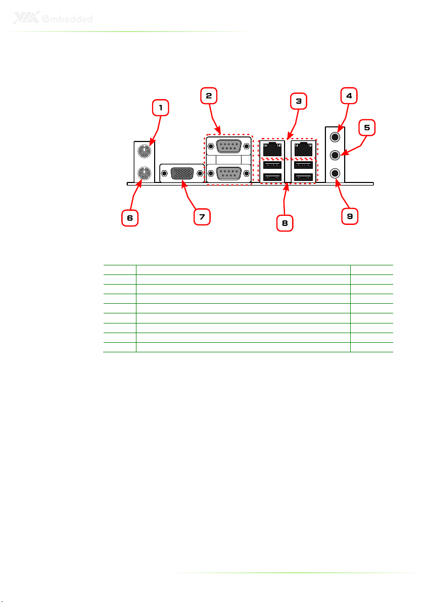
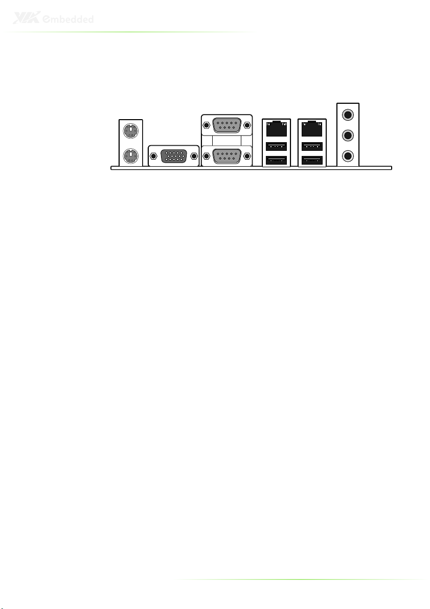
LAYOUT (I/O PANEL)
Item Description Page
1 PS/2 keyboard port 9
2 COM ports 9
3 Gigabit Ethernet ports 9
4 Line-in 3.5 mm TRS jack 9
5 Line-out 3.5 mm TRS jack 9
6 PS/2 mouse port 9
7 VGA port 9
8 USB 2.0 ports 9
9 Microphone 3.5 mm TRS jack 9
5
Page 15

SPECIFICATIONS
Fan
Processor
Chipset
Super I/O
Memory
VGA
Storage
LAN
Audio
I/O
Expansion
Back Panel I/O
BIOS
Operating System
Fan
FanFan
VIA 1.3+GHz Nano processor
running at 1.6 GHz
Fanless
Fanless
FanlessFanless
VIA 1.2GHz Nano processor
running at 1.2 GHz
VIA VX800 Advanced all-in-one system processor
Fintek F81865-I
2 x DDR2 533/667 MHz DIMM slot*
(each slot can support a 2 GB module)
Integrated VIA Chrome9™ HC3 3D/2D graphics
1 x UDMA 133/100 40-pin connector
2 x SATA connectors with configurable pin 7
(GND/5V)
2 x SATA 3.5” HDD auxiliary power
(for DC-in SKU only)
1 x CF type 1
2 x VIA VT6130 PCIe Gigabit Ethernet controller
VIA VT1708S High Definition audio codec
1 x USB pin header (supports two USB ports)
2 x 2-channel 24-bit LVDS connectors
2 x Backlight control connectors
1 x front audio pin header
(Line-in/Mic-in or amplifier module)
1 x PS2 keyboard/mouse pin header
6 x RS232 pin header (configurable 5V/12V)
1 x LPT pin header
1 x LPC pin header
1 x SMBUS pin header
1 x S/PDIF Out connector
1 x SIR pin header
2 x Digital I/O pin header (GPI x 8, GPO x 8)
1 x front panel pin header
2 x Smart Fan connectors
1 x Temperature sensor pin header
1 x ATX power connector or
+12V DC-in (option)
1 x 4-lane PCIe slot
2 x PS/2 connectors (mouse and keyboard)
2 x RS232 COM port (configurable 5V/12V)
1 x VGA port
2 x RJ-45 LAN port
4 x USB ports
3 x Audio jacks (Line-out, Line-in, Mic-in)
Award BIOS
4/8Mbit SPI Flash ROM
Windows CE, XPe, XP, Linux
6
Page 16

System Monitoring
Operating environment
Form Factor
Certifications
Compliance
*System resources require physical memory address locations above 3 GB that may reduce the total available
memory.
**Specifications are subject to change without notice.
- Wake-on-LAN, keyboard power-on, RTC timer,
Watch Dog timer
- System power management
- AC power failure recover
0°C ~ 60°C
0% ~ 95% (relative humidity; non-condensing)
Mini-ITX (17 cm x 17 cm)
CE/FCC
RoHS
7
Page 17

2
Hardware
Installation
8
Page 18
EXTERNAL I/O
The external I/O panel has the following ports:
PS/2 ports
There are two PS/2 ports: one for a keyboard, one for a mouse.
VGA port
The 15-pin VGA port is for connecting to analog displays.
COM ports
There are two 9-pin COM port is for pointing devices or other
serial devices.
Gigabit LAN ports
The mainboard provides two Gigabit Ethernet port controlled
through the VIA VT6130 PCIe Gigabit Ethernet controller.
USB ports
Four standard USB 2.0 ports are provided.
Audio ports
Three 3.5 mm TRS jacks enable connections to Line-out, Line-in,
and Mic-in.
9
Page 19
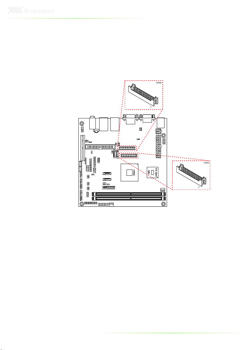
ONBOARD CONNECTORS
LVDS panel connectors
The mainboard has two LVDS panel connectors: LVDS1 and
LVDS2.
10
Page 20
LVDS1
Pin Signal Pin Signal
M1 GND
1 -LD2C0 2 PVDD1
3 +LD2C0 4 PVDD1
5 GND 6 GND
7 -LD2C1 8 GND
9 +LD2C1 10 -LD1C0
11 GND 12 +LD1C0
13 -LD2C2 14 GND
15 +LD2C2 16 -LD1C1
17 GND 18 +LD1C1
19 -LCLK2 20 GND
21 +LCLK2 22 -LD1C2
23 GND 24 +LD1C2
25 -LD2C3 26 GND
27 +LD2C3 28 -LCLK1
29 NC 30 +LCLK1
31 GND 32 GND
33 NC 34 -LD1C3
35 NC 36 +LD1C3
37 NC 38 DVP1_SPCLK
39 NC 40 DVP1_SPD
M2 GND
LVDS2
Pin Signal Pin Signal
M1 GND
1 -A4_L 2 PVDD2
3 A4_L 4 PVDD2
5 GND 6 GND
7 -A5_L 8 GND
9 A5_L 10 -A0_L
11 GND 12 A0_L
13 -A6_L 14 GND
15 A6_L 16 -A1_L
17 GND 18 A1_L
19 -CLK2_L 20 GND
21 CLK2_L 22 -A2_L
23 GND 24 A2_L
25 -A7_L 26 GND
27 A7_L 28 -CLK1_L
29 NC 30 CLK1_L
31 NC 32 GND
33 NC 34 -A3_L
35 NC 36 A3_L
37 NC 38 DISPCLKI0
39 NC 40 DISPCLKO0
M2 GND
11
Page 21
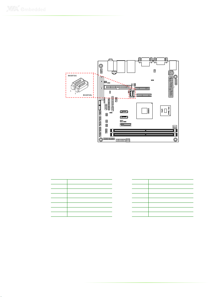
Inverter connectors
The mainboard has two inverters for controlling the LVDS panel
backlight and brightness. INVERTER1 corresponds to the LVDS1
panel connector. INVERTER2 corresponds to the LVDS2 panel
connector.
INVERTER1
Pin Signal Pin Signal
1 IVDD1_CEN 1 IVDD2
2 IVDD1_CEN 2 IVDD2
3 BLON1 3 BAKLITE
4 VX800PWM_CTL 4 VX800PWM_CTL
5 BLON1 5 BAKLITE
6 BRIGHTNESS1_CTL 6 BRIGHTNESS_CTL
7 GND 7 GND
8 GND 8 GND
INVERTER2
12
Page 22
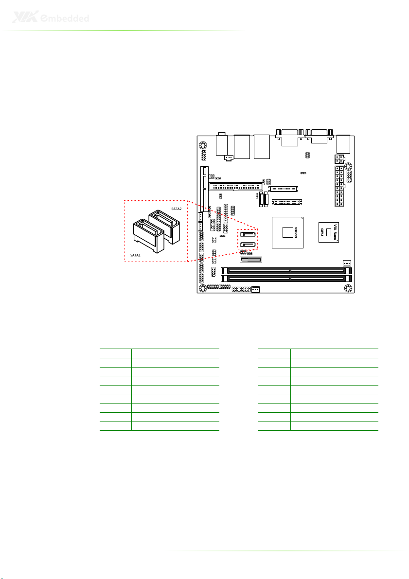
SATA connectors
There are two onboard SATA connectors that support data
transfers speeds up to 3 Gbps. Both 2.5-inch and 3.5-inch SATA
drives can be supported. The standard mainboard version can
only support 2.5-inch SATA hard drives. The DC-in mainboard
version can only support 3.5-inch SATA hard drives.
SATA1
Pin Signal Pin Signal
G1 G1 G1 G1
1 GND 1 GND
2 STXP_1 2 STXP_2
3 STXN_1 3 STXN_2
4 GND 4 GND
5 SRXN_1 5 SRXN_2
6 SRXP_1 6 SRXP_2
7 GND 7 GND
G2 G2 G2 G2
SATA2
13
Page 23
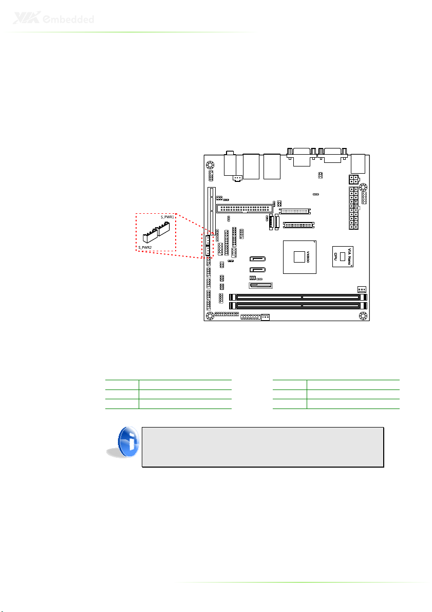
SATA power connectors
The DC-in SKU version of the mainboard provides two 3-pin SATA
power connectors. Each SATA power connector provides an
auxiliary 12V power supply to attached 3.5-inch SATA hard drives.
When connecting SATA power cables to the SATA power
connectors, make sure that the power plugs are inserted in the
proper orientation and the pins are properly aligned.
S_PWR1
Pin Signal Pin Signal
1 +5v 1 +5v
2 +12V 2 +12V
3 GND 3 GND
S_PWR2
Note:
Note:
Note:Note:
The SATA power connectors are only available with the DC-in
SKU.
14
Page 24
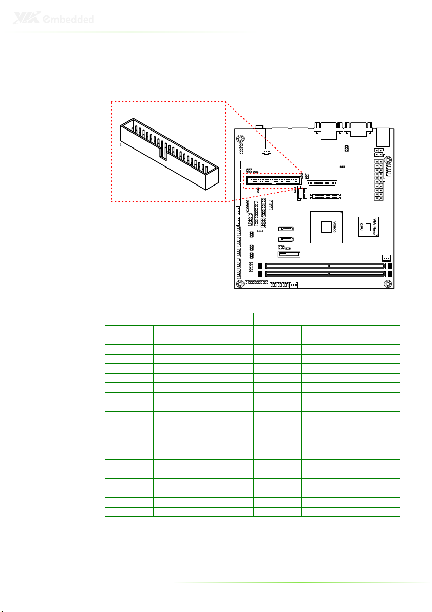
IDE connector
The mainboard has one IDE connector that provides support for
up to two IDE devices.
Pin Signal Pin Signal
1 -IDE_RST 2 GND
3 PD_7 4 PD_8
5 PD_6 6 PD_9
7 PD_5 8 PD_10
9 PD_4 10 PD_11
11 PD_3 12 PD_12
13 PD_2 14 PD_13
15 PD_1 16 PD_14
17 PD_0 18 PD_15
19 GND 20 IDEV_SEL
21 PD_REQ 22 GND
23 -PD_IOW 24 GND
25 -PD_IOR 26 GND
27 PD_RDY 28 GND
29 -PD_ACK 30 GND
31 PD_IRQ15 32 NC
33 PD_A1 34 -LID
35 PD_A0 36 PD_A2
37 -PD_CS1 38 -PD_CS3
39 -HD_LED1 40 GND
15
Page 25
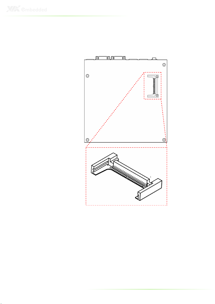
Compact Flash slot
The onboard CompactFlash socket is located on the bottom side
of the mainboard. It is compatible with Type 1 and Type 2
CompactFlash cards.
16
Page 26
PCIe slot
The onboard PCI Express slot supports one PCIe x4 expansion card.
USB pin header
The onboard USB pin header enables the addition of two more
USB 2.0 ports.
Pin Signal Pin Signal
1 VUSB4 2 VUSB4
3 USBD_T2- 4 USBD_T35 USBD_T2+ 6 USBD_T3+
7 GND 8 GND
9 — 10 GND
17
Page 27

RS232 COM pin headers
The mainboard includes six COM pin headers onboard.
Pin Signal Pin Signal
1 COM_DCDX 2 COM_RXDX
3 COM_TXDX 4 COM_DTRX
5 GND 6 COM_DSRX
7 COM_RTSX 8 COM_CTSX
9 COM_RIX 10 —
18
Page 28

Digital I/O pin headers
The mainboard includes two Digital I/O pin headers that support
eight GPO and eight GPI pins.
DIO1
Pin Signal Pin Signal Pin Signal Pin Signal
1 5V_DIO 2 12V_DIO 1 5V_DIO 2 12V_DIO
3 GPO_23 4 GPI_03 3 GPO_27 4 GPI_15
5 GPO_22 6 GPI_02 5 GPO_26 6 GPI_11
7 GPO_21 8 GPI_01 7 GPO_25 8 GPI_10
9 GPO_20 10 GPI_00 9 GPO_24 10 GPI_04
11 GND 12 NC 11 GND 12 NC
DIO2
19
Page 29

LPT pin header
The mainboard includes one onboard LPT pin header.
Pin Signal Pin Signal
1 -LP_STB 2 -LP_AFD
3 LP_D0 4 -LP_ERR
5 LP_D1 6 -LP_INIT
7 LP_D2 8 -LP_SLIN
9 LP_D3 10 GND
11 LP_D4 12 GND
13 LP_D5 14 GND
15 LP_D6 16 GND
17 LP_D7 18 GND
19 -LP_ACK 20 GND
21 LP_BUSY 22 GND
23 LP_PE 24 GND
25 LP_SLCT
20
Page 30

LPC pin header
The mainboard includes one LPC pin header.
Pin Signal Pin Signal
1 LPC_AD1 2 LPC_33_CLK
3 -PCI_RST-1 4 GND
5 LPC_AD0 6 LPC_48_CLK
7 LPC_AD2 8 -LPC_FRAME
9 SERIRQ 10 LPC_AD3
11 -LPC_DRQ1 12 -EXTSMI
13 +5V 14 +3.3V
15 +5V 16 +3.3V
17 GND 18 GND
19 GND 20 —
21
Page 31

FIR pin header
The onboard FIR pin header enables connections to IR optics.
Pin Signal
1 +5V
2 IRRX2
3 IRRX
4 GND
5 IRTX
SMBus pin header
The mainboard includes an SMBus pin header.
Pin Signal
1 SMB_CLK
2 SMB_DAT
3 GND
22
Page 32

MFX pin header
The mainboard includes an MFX pin header.
Pin Signal Pin Signal
1 +5V 2 +5VSUS
3 PW_BN 4 SMB_CLK
5 NC 6 SMB_DAT
7 NC 8 GND
9 GND —
SPI pin header
The onboard SPI pin header provides support for one full-duplex
serial slave device.
Pin Signal Pin Signal
1 SPI_VCC 2 GND
3 SPI_SS0 4 SPI_CLK
5 SPI_DI 6 SPI_DO
7 — 8 RST_SW
23
Page 33

SPDIF connector
The mainboard includes one SPDIF connector.
Pin Signal
1 +5V
2 SPDIF_O
3 GND
PS/2 keyboard and mouse pin header
The mainboard includes one pin header for adding support for
PS/2 keyboard and mouse.
Pin Signal Pin Signal
1 +5VDUAL 2 GND
3 KB_CLK 4 KB_DAT
5 EKBCLK 6 EKBDATA
7 MS_CLK 8 MS_DAT
9 EMSCLK 10 EMSDATA
24
Page 34

Front audio pin header
The mainboard has one pin header for connecting to front panel
switches and status LEDs.
Pin Signal Pin Signal
1 HPOUTR 2 HPOUTL
3 NC 4 NC
5 MIC2IN_R 6 MIC2IN_L
7 — 8 NC
9 AGND 10 AGND
Front panel pin header
The mainboard has one pin header for connecting to front panel
switches and status LEDs.
Pin Signal Pin Signal
1 +5VDUAL 2 +5V
3 +5VDUAL 4 HD_LED
5 -PLED_2 6 PW_BN
7 +5V 8 GND
9 NC 10 RST_SW
11 NC 12 GND
13 SPEAK 14 +5V
15 — 16 -SLEEP_LED
25
Page 35

Memory module slots
The mainboard includes two DIMM memory module slots.
26
Page 36

To install the memory modules:
1. Disengage the locking mechanism at both ends of the
DIMM slot.
2. Align the notch at the bottom of the DIMM with the
counterpart on the DIMM slot.
3. Then insert the DIMM into the slot and push down at
both ends until the locking clips snap into position.
27
Page 37

CPU fan and system fan connectors
CPUFAN1 and SYSFAN1 run on +5V and maintains system
cooling. When connecting the cable to the connector, always be
aware that the red wire (positive wire) should be connected to the
+5V pin. The black wire is the ground wire and should always be
connected to GND.
CPUFAN1
Pin Signal Pin Signal
1 F_IO2 1 F_IO1
2 F_PWM2 2 F_PWM1
3 GND 3 GND
SYSFAN1
Thermal sensor pin header
The onboard battery provides power to the CMOS RAM. If
disconnected all configurations in the CMOS RAM will be reset to
factory defaults. When replacing the battery, use CR2032 coin
batteries.
28
Page 38

ATX power connector
The mainboard supports a conventional ATX power supply for the
power system. Before inserting the power supply connector,
always make sure that all components are installed correctly to
ensure that no damage will be caused. To connect the power
supply, make sure the power plug is inserted in the proper
orientation and the pins are aligned. Then push down the plug
firmly into the connector.
Pin Signal Pin Signal
1 +3.3V 2 +3.3V
3 +3.3V 4 -12V
5 GND 6 GND
7 +5V 8 PS_ON
9 GND 10 GND
11 +5V 12 GND
13 GND 14 GND
15 PW_OK 16 -5V
17 +5V_SB 18 +5V
19 +12V 20 +5V
29
Page 39

DC-in power connector
The mainboard has a 12V DC connector onboard. The 12V DC is
needed if 3.5-inch SATA drives will be used with the mainboard.
Pin Signal Pin Signal
1 GND 3 +12VDC
2 GND 4 +12VDC
CMOS battery
The onboard battery provides power to the CMOS RAM. If
disconnected all configurations in the CMOS RAM will be reset to
factory defaults. When replacing the battery, use CR2032 coin
batteries.
30
Page 40

ONBOARD JUMPERS
LVDS jumper settings
The LVDS connectors and LVDS inverters can operate on different
input voltages. Pins 1, 3, and 5 correspond to INVERTER1. Pins 2, 4,
and 6 correspond to LVDS1.
INVERTER1 power 1 3 5
+12V (default) ON ON OFF
+5V OFF ON ON
LVDS1 power 2 4 6
+3.3V (default) ON ON OFF
+5V OFF ON ON
LVDS2 jumper settings
IVDD2 corresponds to INVERTER2. PVDD2 corresponds to LVDS2.
IVDD2 power 1 2 3
+12V (default) OFF ON ON
+5V ON ON OFF
PVDD2 power 1 2 3
+3.3V (default) OFF ON ON
+5V ON ON OFF
31
Page 41

SATA DOM power select
The J7 jumper enables SATA1 and SATA2 to support +5V on the
seventh SATA pin.
SATA2 setting 1 3 5
+5V ON ON OFF
GND (default) OFF ON ON
SATA1 setting 2 4 6
+5V ON ON OFF
GND (default) OFF ON ON
CF power select
The CF_SEL1 jumper enables the CF slot to support either +3.3V or
+5V.
Voltage setting 1 3 5
+3.3V (default) ON ON OFF
+5V OFF ON ON
Master/slave setting 2 4 6
Slave ON ON OFF
Master OFF ON ON
32
Page 42

IDE DOM power select
The J4 jumper enables the IDE port to support either +3.3V or +5V.
Setting 1 2 3
+3.3V (default) ON ON OFF
+5V OFF ON ON
COM power select
The COM jumpers enable the COM ports to support either +5V or
+12V power modes. All of the COM power select jumpers (J1, J6,
J8, and J9) have identical jumper settings as shown below.
COM setting 1 3 5
+5V (default) ON ON OFF
+12V OFF ON ON
COM setting 2 4 6
+5V (default) ON ON OFF
+12V OFF ON ON
33
Page 43

Clear CMOS jumper
The onboard CMOS RAM stores system configuration data and
has an onboard battery power supply. To reset the CMOS settings,
set the jumper on pins 2 and 3 while the system is off. Return the
jumper to pins 1 and 2 afterwards. Setting the jumper while the
system is on will damage the mainboard. The default setting is on
pins 1 and 2.
Setting 1 2 3
Normal Operation (default) ON ON OFF
Clear CMOS setting OFF ON ON
Caution:
Caution:
Caution:Caution:
Except when clearing the RTC RAM, never remove the cap from
the CLEAR_CMOS jumper default position. Removing the cap
will cause system boot failure. Avoid clearing the CMOS while
the system is on; it will damage the mainboard.
34
Page 44

AT/ATX mode jumper
The AT/ATX jumper enables the user to specify AT or ATX power
mode support. To enable support for +3.3V, the jumper must be
set to ATX mode.
Setting 1 2 3
Normal Operation (default) ON ON OFF
Clear CMOS setting OFF ON ON
35
Page 45

3
BIOS Setup
36
Page 46

ENTERING THE BIOS SETUP MENU
Power on the computer and press <Delete
of the boot sequence to enter the BIOS setup menu. If you missed
the BIOS setup entry point, restart the system and try again.
Delete> during the beginning
DeleteDelete
CONTROL KEYS
Keys Description
Up Move to the previous item
Down Move to the next item
Left Move to the left
Right Move to the right
Enter Select the item
Esc Jumps to the Exit menu or returns to the main menu
Page Up Increase the numeric value or make changes
Page Down Decrease the numeric value or make changes
+ (number pad) Increase the numeric value
- (number pad) Decrease the numeric value
F1 General help, only for Status Page Setup Menu and
F5 Restore the previous CMOS value (only for option page
F6 Load the Fail-safe CMOS values (only for option page
F7 Load Optimized defaults
F10 Save all the changes and exit
from a submenu
Option Page Setup Menu
setup menu)
setup menu)
37
Page 47

GETTING HELP
The BIOS setup program provides a “General Help
can display this screen from any menu/sub-menu by pressing
<F1
F1>. The help screen displays the keys for using and navigating
F1F1
the BIOS setup. Press <Esc
Esc> to exit the help screen.
EscEsc
General Help” screen. You
General HelpGeneral Help
38
Page 48

MAIN MENU
The Main Menu contains twelve setup functions and two exit
choices. Use arrow keys to select the items and press <Enter
accept or enter Sub-menu.
Standard CMOS Features
Use this menu to set basic system configurations.
Advanced BIOS Features
Use this menu to set the advanced features available on your
system.
Enter> to
EnterEnter
Advanced Chipset Features
Use this menu to set chipset specific features and optimize system
performance.
Integrated Peripherals
Use this menu to set onboard peripherals features.
Power Management Setup
Use this menu to set onboard power management functions.
PnP/PCI Configurations
Use this menu to set the PnP and PCI configurations.
39
Page 49

PC Health Status
This menu shows the PC health status.
Frequency/Voltage Control
Use this menu to set the system frequency and voltage control.
Load Optimized Defaults
Use this menu option to load BIOS default settings for optimal and
high performance system operations.
Set Supervisor Password
Use this menu option to set the BIOS supervisor password.
Set User Password
Use this menu option to set the BIOS user password.
Save & Exit Setup
Save BIOS setting changes and exit setup.
Exit Without Saving
Discard all BIOS setting changes and exit setup.
40
Page 50

STANDARD CMOS FEATURES
Date
The date format is [Day, Month Date, Year]
Time
The time format is [Hour : Minute : Second]
Video
Settings Description
EGA/VGA Supports 16 colors at 640x350 and 640x480 resolutions
CGA 40 Supports 16 colors at 320x200 resolution
CGA 80 Supports 16 colors at 640x200 resolution
MONO Supports 1 color at 80x25 characters (columns x rows)
Halt On
Set the system’s response to specific boot errors. Below is a table
that details the possible settings.
Settings Description
All Errors System halts when any error is detected
No Errors System does not halt for any error
All, But Keyboard System halts for all non-key errors
41
Page 51

HDD CHANNELS
The specifications of your drive must match with the drive table.
The hard disk will not work properly if you enter incorrect
information in this category. Select “Auto
you select “Manual
Manual”, make sure the information is from your hard
ManualManual
disk vendor or system manufacturer.
Below is a table that details required hard drive information when
using the “Manual
Settings Description
[storage] Channel The name of this match the name of the menu.
Access Mode Settings: [CHS, LBA, Large, Auto]
Capacity Formatted size of the storage device
Cylinder Number of cylinders
Head Number of heads
Precomp Write precompensation
Landing Zone Cylinder location of the landing zone
Sector Number of sectors
Manual” mode.
ManualManual
Settings: [None, Auto, Manual]
Auto” whenever possible. If
AutoAuto
42
Page 52

ADVANCED BIOS FEATURES
Virus Warning
Enables boot sector protection for the hard disks.
Settings Description
Enabled Turns on hard disk boot sector virus protection
Disabled Turns off hard disk boot sector virus protection
Note:
Note:
Note:Note:
If this function is enabled and someone attempt to write data
into this area, the BIOS will sound off an audible alarm and
show a warning message on the screen.
CPU L1 & L2 Cache
Settings Description
Disabled Turns off CPU L1 & L2 cache
Enabled Turns on CPU L1 & L2 cache
CPU L2 Cache ECC Checking
Settings Description
Disabled Turns off ECC checking
Enabled Enables the system to detect and correct single-bit errors
43
Page 53

Quick Power On Self-Test
Shortens the Power On Self-Test (POST) cycle to enable a faster
boot up time.
Settings Description
Disabled Standard Power On Self Test (POST)
Enabled Shorten Power On Self Test (POST) cycle and boot up
time
First/Second/Third Boot Device
Sets the boot device sequence as the BIOS attempts to load the
disk operating system.
Settings Description
LS120 Boot from LS-120 drive
Hard Disk Boot from the HDD
CDROM Boot from CDROM
ZIP100 Boot from ATAPI ZIP drive
USB-FDD Boot from USB Floppy drive
USB-ZIP Boot from USB ZIP drive
USB-CDROM Boot from USB CDROM
Legacy LAN Boot from network drive
Disabled Disable the boot device sequence
Boot Other Device
Enables the system to boot from alternate devices if the system fails
to boot from the “First/Second/Third Boot Device” lists.
Settings Description
Disabled No alternate boot device allowed
Enabled Enable alternate boot device
Boot Up NumLock Status
Sets the NumLock status when the system is powered on.
Settings Description
Off Forces keypad to behave as arrow keys
On Forces keypad to behave as 10-key
Typematic Rate Setting
Enables “Typematic Rate” and “Typematic Delay” functions.
Settings Description
Disabled Forces default typematic rate and delay
Enabled Unlocks Typematic Rate and Typematic Delay
44
Page 54

Typematic Rate (Chars/Sec)
This item sets the rate (characters/second) at which the system
retrieves a signal from a depressed key.
Settings: [6, 8, 10, 12, 15, 20, 24, 30]
Typematic Delay (Msec)
This item sets the delay between, when the key was first pressed
and when the system begins to repeat the signal from the
depressed key.
Settings: [250, 500, 750, 1000]
Security Option
Selects whether the password is required every time the System
boots, or only when you enter Setup.
Settings Description
Setup Password prompt appears only when end users try to run
BIOS Setup
System Password prompt appears every time when the computer is
powered on and when end users try to run BIOS Setup
MPS Version Control for OS
Settings: [1.1, 1.4]
OS Select for DRAM > 64MB
Select OS2 only if you are running OS/2 operating system with
greater than 64MB of RAM on the system.
Settings: [Non-OS2, OS2]
HDD S.M.A.R.T Capability
Settings: [Disabled, Enabled]
Video BIOS Shadow
Copies the Video BIOS to the shadow RAM to improve
performance.
Settings: [Disabled, Enabled]
45
Page 55

Full Screen Logo Show
Show full screen logo during BIOS boot up process.
Settings: [Disabled, Enabled]
Summary Screen Show
Show summary screen.
Settings: [Disabled, Enabled]
46
Page 56

CPU FEATURES
Thermal Management
This item sets CPU’s thermal control rule to protect the CPU from
overheating.
Settings Description
Thermal Monitor 3 Dynamic Ratio and VID
Disabled
47
Page 57

HARD DISK BOOT PRIORITY
This is for setting the priority of the hard disk boot order when the
“Hard Disk” option is selected in the “[First/Second/Third] Boot
Device” menu item.
48
Page 58

ADVANCED CHIPSET FEATURES
Caution:
Caution:
Caution:Caution:
The Advanced Chipset Features menu is used for optimizing the
chipset functions. Do not change these settings unless you are
familiar with the chipset.
Memory Hole
Settings: [Disabled, 15M – 16M]
System BIOS Cacheable
Settings: [Disabled, Enabled]
Video RAM Cacheable
Settings: [Disabled, Enabled]
49
Page 59

INTERNAL VGA CONTROL
VGA Share Memory Size
This setting allows you to select the amount of system memory
that is allocated to the integrated graphics processor.
Settings: [Disabled, 64M, 128M, 256M]
Direct Frame Buffer
Settings: [Disabled, Enabled]
Select Display Device
This feature enables choosing between different types of display
outputs. The default setting is CRT+LCD. When set in the LCD
mode, the CRT display must be connected before turning on the
power. Otherwise, the CRT display will be ignored.
Settings Description
CRT Enables the VGA port
LCD Enables LVDS1
LCD2 Enables LVDS2
CRT+LCD Enables VGA and LVDS1
CRT+LCD2 Enables VGA and LVDS2
LCD+LCD2 Enables LVDS1 and LVDS2
50
Page 60

Panel Type
Panel ID Resolution
0 640x480
1 800x600
2 1024x768
3 1280x768
4 1280x1024
5 1400x1050
6 1440x900
7 1280x800
8 800x480
9 1024x600
A 1366x768
B 1600x1200
C 1680x1050
D 1920x1200
E 640x240
F 480x640
51
Page 61

CPU & PCI BUS CONTROL
PCI Master 0 WS Write
Settings: [Enabled, Disabled]
PCI Delay Transaction
Settings: [Disabled, Enabled]
52
Page 62

INTEGRATED PERIPHERALS
Onboard LAN Boot ROM
Settings: [Enabled, Disabled]
53
Page 63

VIA ONCHIP IDE DEVICE
CF Card UDMA66
Settings: [Disabled, Enabled]
SATA Controller
Settings: [Disabled, Enabled]
IDE DMA Transfer Access
Settings: [Disabled, Enabled]
OnChip IDE Channel 1
Settings: [Disabled, Enabled]
IDE Prefetch Mode
Settings: [Disabled, Enabled]
Secondary Master PIO
Settings: [Auto, Mode 0, Mode 1, Mode 2, Mode 3, Mode 4]
Secondary Slave PIO
Settings: [Auto, Mode 0, Mode 1, Mode 2, Mode 3, Mode 4]
Secondary Master UDMA
Settings: [Disabled, Auto]
54
Page 64

Secondary Slave UDMA
Settings: [Disabled, Auto]
IDE HDD Block Mode
Settings: [Disabled, Enabled]
55
Page 65

VIA ONCHIP PCI DEVICE
Azalia HDA Controller
Settings: [Auto, Disabled]
56
Page 66

SUPERIO DEVICE
Serial ports
The SuperIO Device configuration menu enables the BIOS to
specifically define the resources used for serial ports 1 – 4.
Port Address IRQ
1 1F8, 1E8 5, 10
2 1F8, 1E8, 5, 10
3 3F8, 2F8, 3E8, 2E8, 338, 348, Disabled, Auto 4
4 3F8, 2F8, 3E8, 2E8, 338, 348, Disabled, Auto 4
5 3F8, 2F8, 3E8, 2E8, 338, 348, Disabled, Auto 4
6 3F8, 2F8, 3E8, 2E8, 338, 348, Disabled, Auto 4
7 3F8, 2F8, 3E8, 2E8, 338, 348, Disabled, Auto 4
8 3F8, 2F8, 3E8, 2E8, 338, 348, Disabled, Auto 4
Onboard Parallel Port
This specifies the I/O port address and IRQ of the onboard parallel
port.
Settings: [Disabled, 378/IRQ7, 278/IRQ5, 3BC/IRQ7]
57
Page 67

Parallel Port Mode
Set the parallel port mode. To operate the onboard parallel port as
Standard Parallel Port, choose SPP. To operate the onboard parallel
port in the EPP mode, choose EPP. By choosing ECP, the onboard
parallel port will operate in ECP mode. Choosing ECP + EPP will
allow the onboard parallel port to support both the ECP and EPP
modes simultaneously.
Settings: [SPP, EPP, ECP, ECP + EPP]
ECP Mode Use DMA
ECP (Extended Capabilities Port) has two DMA channels that it can
use. The default channel is 3. However, some expansion cards
may use channel 3 as well. To solve this conflict, change the ECP
channel to 1. Select a DMA channel for the port.
Settings: [1, 3]
Internal IrDA Controller
Enables or disables the infrared port.
Settings: [Disabled, FIR]
IR IRQ
Set this field to reserve an IRQ for the Fast IR port. This field is only
available if Onboard Fast IR is enabled. The Fast IR IRQ is locked to
IRQ 11.
IR DMA
Set this field to choose the DMA channel. This field is only available
if Onboard Fast IR is enabled. The Fast IR DMA is locked to 6.
58
Page 68

USB DEVICE SETTING
USB 1.0 Controller
Enable or disable Universal Host Controller Interface for Universal
Serial Bus.
Settings: [Disabled, Enabled]
USB 2.0 Controller
Enable or disable Enhanced Host Controller Interface for Universal
Serial Bus.
Settings: [Disabled, Enabled]
USB Operation Mode
Auto decide USB device operation mode.
Settings Description
Full/Low Speed All of USB Device operated on full/low speed mode
High Speed If USB device was high speed device, then it operated
on high speed mode.
USB Keyboard Function
Enable or disable legacy support of USB keyboard.
Settings: [Disabled, Enabled]
USB Mouse Function
Settings: [Disabled, Enabled]
59
Page 69

USB Storage Function
Enable or disable legacy support of USB mass storage.
Settings: [Disabled, Enabled]
60
Page 70

POWER MANAGEMENT SETUP
ACPI Suspend Type
Settings Description
S1(POS) S1/Power On Suspend (POS) is a low power state. In this
state, no system context (CPU or chipset) is lost and
hardware maintains all system contexts.
S3(STR) S3/Suspend To RAM (STR) is a power-down state. In this
state, power is supplied only to essential components
such as main memory and wakeup-capable devices. The
system context is saved to main memory, and context is
restored from the memory when a "wakeup" event
occurs.
S1 & S3 Depends on the OS to select S1 or S3.
Power Management Option
When set to “Max Saving”, the HDD will power down if inactive
for 5 minutes and the system will go into suspend mode if inactive
for 30 seconds.
When set to “Min Saving”, the HDD will power down if inactive for
15 minutes and the system will go into suspend mode if inactive
for 1 hour.
Settings: [User Define, Min Saving, Max Saving]
61
Page 71

HDD Power Down
Set the length of time for a period of inactivity before powering
down the hard disk.
Settings: [Disable, 1 Min, 2 Min, 3 Min, 4 Min, 5 Min, 6 Min, 7 Min,
8 Min, 9 Min, 10 Min, 11 Min, 12 Min, 13 Min, 14 Min, 15 Min]
Suspend Mode
Sets the length of time for a period of inactivity before entering
suspend mode.
Settings: [Disable, 1 Min, 2 Min, 4 Min, 6 Min, 8 Min, 10 Min, 20
Min, 30 Min, 40 Min, 1 Hour]
Video Off Option
Select whether or not to turn off the screen when system enters
power saving mode, ACPI OS such as Windows XP will override
this option.
Settings Description
Always On Screen is always on even when system enters power
saving mode
Suspend -> Off Screen is turned off when system enters power saving
mode
Video Off Method
Settings: [Blank Screen, V/H SYNC+Blank, DPMS Support]
MODEM Use IRQ
Settings: [NA, 3, 4, 5, 7, 9, 10, 11]
Soft-Off by PWRBTN
This field configures the power button on the chassis.
Settings Description
Delay 4 Sec System is turned off if power button is pressed for
more than four seconds.
Instant-Off Power button functions as a normal power-on/-off
button.
62
Page 72

Run VGABIOS if S3 Resume
Select whether to run VGA BIOS if resuming from S3 state. This is
only necessary for older VGA drivers.
Settings: [Auto, Yes, No]
AC Loss Auto Restart
The field defines how the system will respond after an AC power
loss during system operation.
Settings Description
Off Keeps the system in an off state until the power button is
pressed
On Restarts the system when the power is back
Former-Sts Former-Sts
WatchDog Run/Stop
Settings: [Stop, Run]
WatchDog Count Value
Key in a DEC number.
Settings: [Min = 0, Max = 1023]
63
Page 73

WAKEUP EVENT DETECT
PS2KB Wakeup Select
This feature has two settings: Hot Key and Password. To select the
Password option, press <Page Up> or <Page Down>. To set the
password, enter up to eight digits and press <Enter>.
Settings: [Hot Key]
PS2KB Wakeup Key Select
This feature is only available when “Hot Key” is chosen in “PS2KB
Wakeup Select”.
Settings: [Ctrl+F1, Ctrl+F2, Ctrl+F3, Ctrl+F4, Ctrl+F5, Ctrl+F6, Ctrl+F7,
Ctrl+F8, Ctrl+F9, Ctrl+F10, Ctrl+F11, Ctrl+F12, Power, Wake, Any
Key]
PS2MS Wakeup Key Select
Settings: [Any Button, Left Button, Right Button]
PS2 Keyboard Power ON
Settings: [Disabled, Enabled]
PS2 Mouse Power ON
Settings: [Disabled, Enabled]
64
Page 74

RTC Alarm Resume
Set a scheduled time and/or date to automatically power on the
system.
Settings: [Disabled, Enabled]
Date (of Month)
The field specifies the date for “RTC Alarm Resume”.
Key in a DEC number.
Settings: [Min = 0, Max = 31]
Resume Time (hh : mm : ss)
The field specifies the time for “RTC Alarm Resume”.
Key in a DEC number.
Settings: [Min = 0, Max = 23]
65
Page 75

PNP/PCI CONFIGURATIONS
Note:
Note:
Note:Note:
This section covers some very technical items and it is strongly
recommended to leave the default settings as is unless you are
an experienced user.
Init Display First
Settings: [Onboard, PCIEx]
PNP OS Installed
Settings Description
No BIOS will initialize all the PnP cards
Yes BIOS will only initialize the PnP cards used for booting
(VGA, IDE, SCSI). The rest of the cards will be initialized
by the PnP operating system
Reset Configuration Data
Settings Description
Disabled Default setting
Enabled Resets the ESCD (Extended System Configuration Data)
after exiting BIOS Setup if a newly installed PCI card or
the system configuration prevents the operating system
from loading
66
Page 76

Resources Controlled By
Enable the BIOS to automatically configure all the Plug-and-Play
compatible devices.
Settings Description
Auto(ESCD) BIOS will automatically assign IRQ, DMA and memory
base address fields
Manual Unlocks “IRQ Resources” for manual configuration
PCI/VGA Palette Snoop
Some non-standard VGA display cards may not show colors
properly. This field allows you to set whether MPEG ISA/VESA
VGA Cards can work with PCI/VGA or not. When enabled, a
PCI/VGA can work with a MPEG ISA/VESA VGA card. When
disabled, a PCI/VGA cannot work with a MPEG ISA/VESA Card.
Settings: [Disabled, Enabled]
Assign IRQ for VGA
Assign IRQ for VGA devices.
Settings: [Disabled, Enabled]
Assign IRQ for USB
Assign IRQ for USB devices.
Settings: [Disabled, Enabled]
Maximum Payload Size
Set maximum TLP payload size for the PCI Express devices. The
unit is byte.
Settings: [128, 256, 512, 1024, 2048, 4096]
67
Page 77

IRQ RESOURCES
IRQ Resources list IRQ 3/4/5/7/9/10/11/12/14/15 for users to set
each IRQ a type depending on the type of device using the IRQ.
Settings Description
PCI Device For Plug-and-Play compatible devices designed for PCI bus
architecture
Reserved The IRQ will be reserved for further requests
68
Page 78

PC HEALTH STATUS
The PC Health Status displays the current status of all of the
monitored hardware devices/components such as CPU voltages,
temperatures and fan speeds.
69
Page 79

FREQUENCY/VOLTAGE CONTROL
DRAM Frequency
Settings: [DDR2-400, DDR2-533, DDR-667, SPD]
DDR CAS Latency Control
Settings: [2T, 3T, 4T, 5T, 6T, SPD]
DDR Burst Length
Settings: [4, 8, SPD]
DDR 1T Command Rate
Settings: [Disabled, Enabled]
DRDY Table
Settings: [Slowest, Optimize]
ODT
Settings: [Disabled, Enabled]
70
Page 80

Spread Spectrum
When the mainboard's clock generator pulses, the extreme values
(spikes) of the pulses create EMI (Electromagnetic Interference).
The Spread Spectrum function reduces the EMI generated by
modulating the pulses so that the spikes of the pulses are reduced
to flatter curves. If the system is not placed near EMI sensitive
electronics, it is recommended to leave this feature disabled.
Settings Description
0.1 – 0.9% Increments of 0.1. Higher percentages have a greater
Disabled Support for this feature will be unavailable.
effect on reducing EMI.
71
Page 81

LOAD OPTIMIZED DEFAULTS
This option is for restoring all the default optimized BIOS settings.
The default optimized values are set by the mainboard
manufacturer to provide a stable system with optimized
performance.
Entering “YYYY” and press <Enter> to load the default optimized BIOS
values.
Entering ”NNNN” will cancel the load optimized defaults request.
72
Page 82

SET SUPERVISOR/USER PASSWORD
This option is for setting a password for entering BIOS Setup.
When a password has been set, a password prompt will be
displayed whenever BIOS Setup is run. This prevents an
unauthorized person from changing any part of your system
configuration.
There are two types of passwords you can set. A supervisor
password and a user password. When a supervisor password is
used, the BIOS Setup program can be accessed and the BIOS
settings can be changed. When a user password is used, the
BIOS Setup program can be accessed but the BIOS settings cannot
be changed.
To set the password, type the password (up to eight characters in
length) and press <Enter>
previously set password from CMOS memory. The new password
will need to be reentered to be confirmed. To cancel the process
press <Esc>
<Esc>.
<Esc><Esc>
To disable the password, press <Enter>
new password. A message will show up to confirm disabling the
password. To cancel the process press <Esc>
Additionally, when a password is enabled, the BIOS can be set to
request the password each time the system is booted. This would
prevent unauthorized use of the system. See “Security Option” in
the “Advanced BIOS Features” section for more details.
<Enter>. The password typed now will clear any
<Enter><Enter>
<Enter> when prompted to enter a
<Enter><Enter>
<Esc>.
<Esc><Esc>
73
Page 83

SAVE & EXIT SETUP
Entering “YYYY” saves any changes made, and exits the program.
Entering “NNNN” will cancel the exit request.
74
Page 84

EXIT WITHOUT SAVING
Entering “YYYY’ discards any changes made and exits the program.
Entering “NNNN” will cancel the exit request.
75
 Loading...