

Page 1
▪ 4 x USB 2.0 ports
▪ 1 x DisplayPort
▪ 1 x RJ-45 LAN port (Gigabit Ethernet)
▪ 6 x Audio jacks (support multi-channel audio outputs)
▪ 1 x FIR pin header
▪
1 x Serial pin header with 2 sets of TX and RX signals
▪
2 x COM pin headers (support 2 COM ports with +5V/+12V
power select option RI pin)
▪
1 x LPT pin header
▪
1 x SPI pin header
▪
1 x LPC pin header
▪
1 x DIO1 pin header, shared with SDIO connector
▪
1 x DIO2 pin header (from VIA VT1211)
▪
1 x SMBus pin header
▪
1 x I²C pin header
▪
2 x USB 2.0 pin headers for four USB 2.0 ports
▪ 1 x Panel Power Select pin header
▪ 1 x Front LAN LED pin header
▪ 1 x Front Audio pin header
▪
1 x Front Panel pin header for HDD LED, Power LED, Switch
and Speaker
▪ 1 x LVDS connector
▪
1 x Inverter connector
▪
1 x CD-In with housing connector
▪ 1 x SPDIF with housing connector
▪ 1 x SD card socket, shared with DIO1 pin header
▪ 1 x ATX power connector
▪
1 x AUX power connector
▪ 2 x SATA connectors
▪
1 x CPU fan connector
▪
1 x System fan connector
▪ 1 x PCIe x1 slot
▪
2 x MiniPCIe sockets
USB ▪
8 x USB 2.0 ports
DisplayPort Interface ▪
1 x DisplayPort (without HDCP support)
HDMI® Interface ▪
1 x HDMI® port (optional)
LVDS Interface ▪
1 x LVDS channel supports single-channel 8-bit or
24-bit LVDS panel
BIOS ▪
AMI BIOS
▪
4/8Mbit SPI flash memory
Operating System ▪
Microsoft Windows 7/WES7, XP/XPe and CE 6.0
▪
Linux
Hardware Monitoring ▪
CPU temperature reading
▪
CPU fan speed reading
▪
System voltage monitoring
System Memory ▪
Onboard 1GB DDR3/DDR3L 1066
COMe-8X91
COM Express Module
and
COMEDB3
Carrier Board Reference
COM Express Module Type
▪ Support Mini Form Factor Type 10
COMEDB3 Carrier Board Specifications
▪ VIA VT2021 High Definition Audio Codec
▪ VIA VT1211 LPC Super IO
▪ AMI BIOS
▪ 4/8M bit LPC Flash BIOS, PLCC 32 pin or SPI BIOS
Audio
Super I/O
BIOS
Onboard Jumper
▪ 1 x Clear CMOS jumper
▪
1 x Inverter Voltage Select jumper
▪
1 x Panel Power Select jumper
▪
1 x COM Voltage Select jumper
▪ 2 x BIOS Type Select jumpers (for select LPC/SPI BIOS)
▪ 2 x BIOS Select jumper (for select Module/Carrier board BIOS)
▪ 6 x USB Select jumper (for select USB header/MiniPCIe)
Rear I/O Connectors and Ports
Switch
▪ 1 x Power button switch
▪
1 x Reset switch
Operating and Storage Humidity
▪ 95% relative humidity
Storage Temperature
▪ -40°C up to 70°C
Operating System
▪ Microsoft Windows 7, XP, XPe, WinCE 6.0, WES7
▪
Linux
Form Factor and Dimension
▪ Mini-ITX
▪
6 layers
▪
17 cm x 17 cm
Expansion Buses ▪
1 x System Management Bus (SMBus) interface
▪
1 x I²C bus (default for Eup LAN control)
▪
1 x SDIO interface (by default)
▪ 1 x GPIO interface with 4 INs and 4 OUTs (shared with
SDIO)
▪ 1 x LPC bus interface
▪ 1 x SPI
▪ Support Express Card, speaker out, reset function,
thermal protection, suspend/wake signals, power
button, power good and fan control signals
Serial ▪
2 x Serial ports with TX and RX signals
SATA ▪
2 x SATA 3.0 Gbps ports
WatchDog Timer ▪
Software Programmable
Chipset ▪
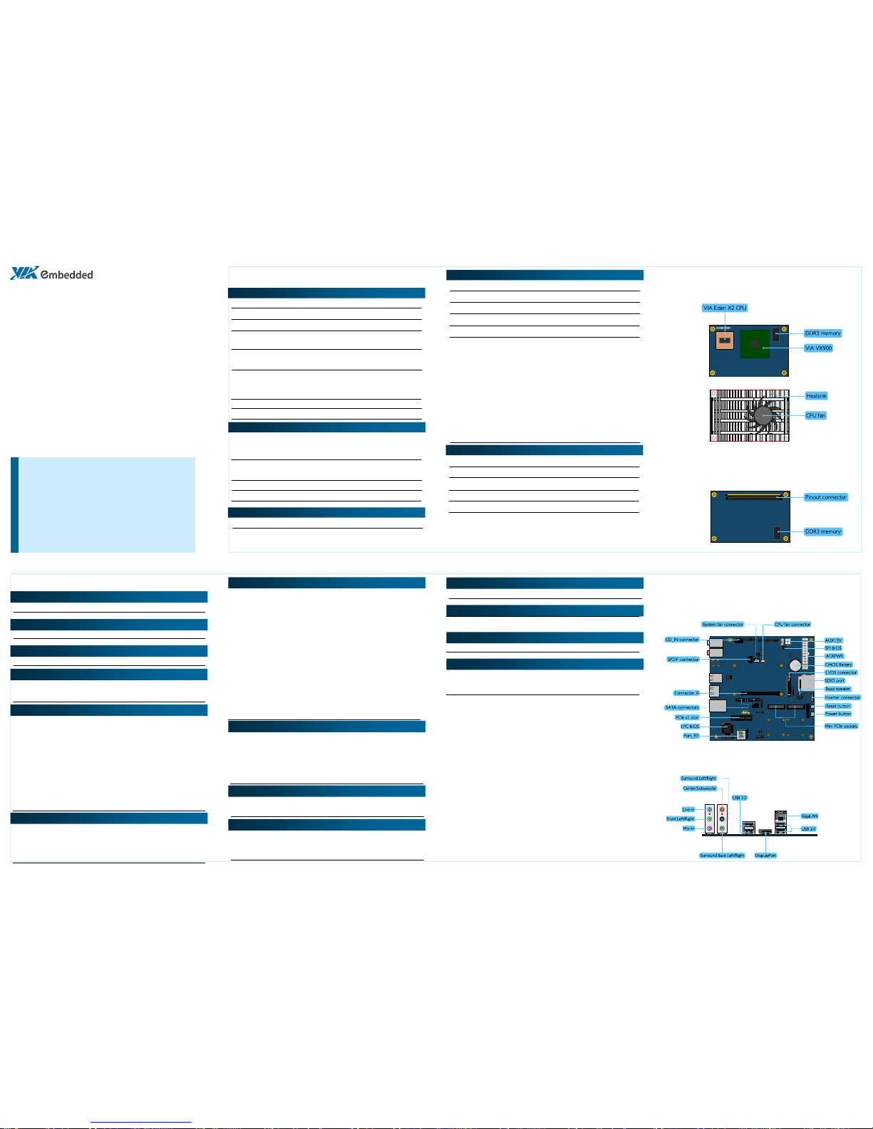
VIA VX900 all-in one system processor
Core
Processor ▪
VIA Eden X2 800 MHz NanoBGA2 CPU
COMe-8X91 Module Specifications
VGA ▪
Integrated VIA C-9 HD DX9 2D/3D graphics
processor and unified video decoding accelerator
Chipset ▪
VIA VT6130 Gigabit Ethernet controller
Operating Humidity ▪
0% to 95% (relative humidity; non-condensing)
Storage Temperature ▪
-40°C to 70°C
COM Express Compliance ▪
COM Express™ Type 10, Mini Module
Dimension ▪
55 mm x 84 mm
Operating Temperature ▪
0°C up to 50°C
Graphics and Video
Ethernet
Mechanical and Environment
Key Features:
• VIA Eden™ X2 processor
• Onboard DDR3 SODIMM memory
• Integrated VIA C-9 HD DX9 2D/3D graphics processor
• Support PCIe x1 and Mini PCIe sockets
• Display interface in 18/24-bit single-channel LVDS panel and
one DisplayPort
• Support USB 2.0 and GigaLAN
Top View
Bottom View
Rear I/O Ports
Onboard Ports and Connectors
Quick Guide
Onboard Pin Headers
Operating Temperature
▪ 0°C up to 50°C
COMEDB3 Carrier Board Layout
Expansion Bus ▪
3 x PCIe Gen2 x1
Audio ▪
1 x HD audio digital interface
LAN ▪
1 x LAN port
Input / Output
Onboard Connectors, Ports and Sockets
COMe-8X91 Module Layout
Page 2
VIA Technologies, Inc.
1F, 531, Zhong-zheng Road, Xindian District,
New Taipei City 231, Taiwan
Tel: 886-2-2218-5452
Fax: 886-2-2218-5453
Web: www.via.com.tw
Note:
Make sure the thermal grease/paste has been applied on top of the
processor and chipset before installing the heatsink.
5V_DIO1 1 2 12V_DIO1
COM_GPO0 3 4 COM_GPI0
COM_GPO1 5 6 COM_GPI1
COM_GPO2 7 8 COM_GPI2
COM_GPO3 9 10 COM_GPI3
GND 11 12 GND
DIO1
5
1 I2C_CLK
2 I2C_DATA
3 GND
I2C_BUS
14
1 SMB_CLK
2 SMB_DATA
3 GND
SMBUS
10
MIC2_FR_L 1 2 AGND
MIC2_FR_R 3 4 FNT_DET
HP_OUT_R 5 6 MIC2_JD
FNT_IO_SENSE 7 8 KEY
HP_OUT_L 9 10 L INE2_JD
+12V 11 12 +12V
AGND 13 14 AGND
F_AUDIO
1
-LP_STB 1 2 -LP_AFD
LP_D0 3 4 -LP_ERR
LP_D1 5 6 -LP_INIT
LP_D2 7 8 -LP_SLIN
LP_D3 9 10 GND
LP_D4 11 12 GND
LP_D5 13 14 GND
LP_D6 15 16 GND
LP_D7 17 18 GND
-LP_ACK 19 20 GND
LP_BUSY 21 22 GND
LP_SLCT 25 26 KEY
LP_PE 23 24 GND
LPT
3
LPC_AD1 1 2 LPC_33M_CLK
-LPC_RESET 3 4 GND
LPC_AD0 5 6 NC
LPC_AD2 7 8 -LPC_FRAME
LPC_SERIRQ 9 10 LPC_AD3
-LPC_DRQ1 11 12 NC
+5V 13 14 +3.3V
+5V 15 16 +3.3V
GND 17 18 GND
GND 19 20 KEY
LPC
11
DIO2
2
5V_DIO2 1 2 12V_DIO2
SIO_GPO30 3 4 SIO_GPI34
SIO_GPO31 5 6 SIO_GPI35
SIO_GPO32 7 8 SIO_GPI36
SIO_GPO33 9 10 SIO_GPI37
GND 11 12 GND
FP_5V 1 2 FP_3V
FP_5V 3 4 -SATA_LED
-PLED 5 6 -SLEEP_LED
FP_5V 7 8 GND
NC 9 10 RST_SW
NC 11 12 GND
SPEAK 13 14 FP_5V
KEY 15 16 NC
F_PANEL
6
VUSB 1 2 VUSB
USBD_T4- 3 4 USBD_T5-
USBD_T4+ 5 6 USBD_T5+
GND 7 8 GND
KEY 9 10 W_LESS_LED
GND 11 12 -RF_ON
USB_4/5
7
SER0_TX_CON 1 2 SER0_RX_CON
NC 3 4 NC
GND 5 6 NC
SER1_TX_CON 7 8 SER1_RX_CON
NC 9 10 KEY
SER_PORT
9
VUSB 1 2 VUSB
USBD_T6- 3 4 USBD_T7-
USBD_T6+ 5 6 USBD_T7+
GND 7 8 GND
KEY 9 10 GND
USB_6/7
12
3VSUS 1 2 -LAN_ACT
3VSUS 3 4 NC
GND 5 6 W_LAN_LED
3VSUS 7 8 GND
KEY 9 10 GND
FLAN_LED
8
SPI_VCC 1 2 GND
-SPI_SS0 3 4 SPI_CLK
SPI_DI 5 6 SPI_DO
KEY 7 8 RESET
SPI
4
28
Pins Description
1-2 Enabled COM2 pin header to support +5V.
2-3 Normal (default)
3-4 Enabled COM2 pin header to support +12V.
JP_COM2_VSEL
29
Pins Description
1-2 Enable d COM1 connector to support +5V.
2-3 Normal (defau lt)
3-4 Enable d COM1 connector to support +12V.
JP_COM1_VSEL
Pins Description
1-2 Keep CMOS settings (default)
2-3 Clear CMOS settings
21
CLEAR_CMOS
Pins Description
1-2 Use +5V for the Inverter power.
2-3 Use +12V for the Inverter power. (default)
23
IVDD
19
BIOS_DIS0
BIOS_DIS0 BIOS_DIS1
Pins Description
1-2 1-2 Select module SPI BIOS (default)
2-3 1-2 Select carrier board LPC BIOS
2-3 2-3 Select carrier board SPI BIOS
20
BIOS_DIS1
Pins Description
1-2 Use +5V for the LCD panel power.
2-3 Use +3.3V for the LCD panel power. (default)
22
PVDD
Copyright © 2013 VIA Technologies, Inc. All rights reserved.
For more information on this and other VIA
products, please visit www.viaembedded.com
For further support and service, please visit
www.via.com.tw
17
18
BIOS_SEL1
BIOS_SEL1 BIOS_SEL0
Pins Description
2-3 1-2 Select module SPI BIOS (default)
2-3 1-2 Select carrier board SPI BIOS
1-2 2-3 Select carrier board LPC BIOS
BIOS_SEL0
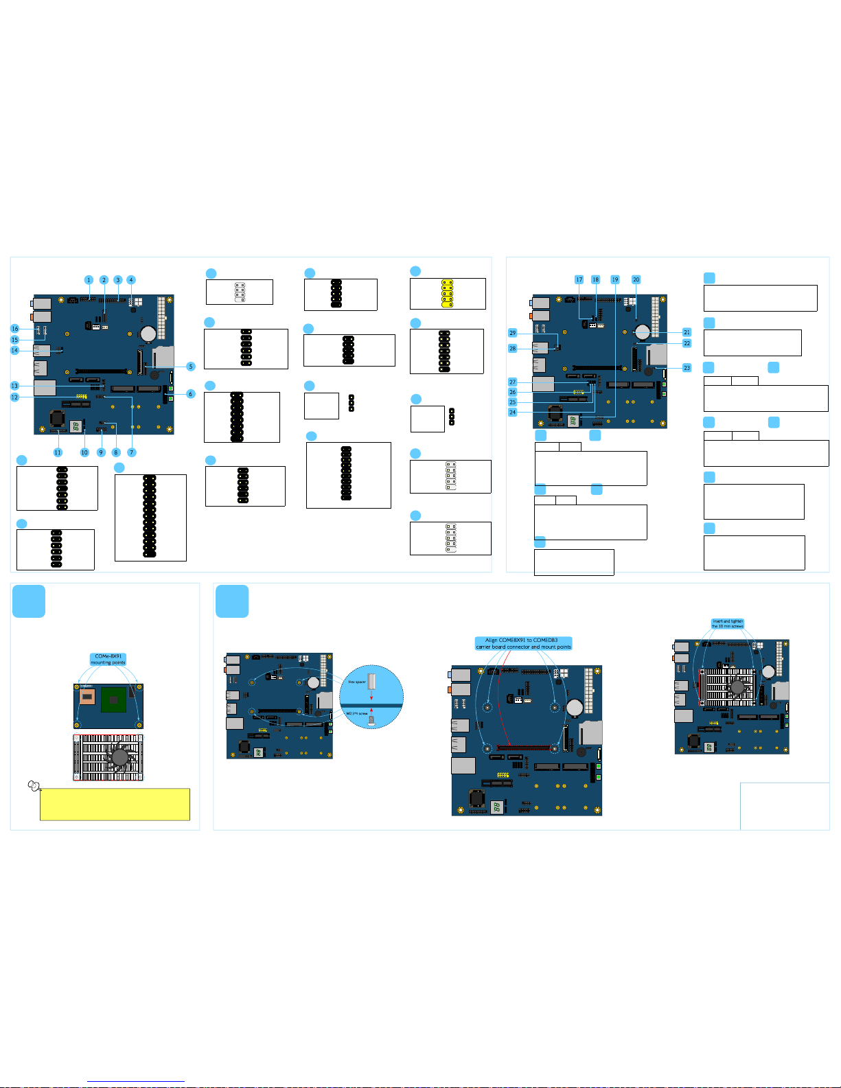
Installing heatsink with fan
1
Step 1
Align the heatsink over the heatsink mounting hole on the COMe-8X91.
Installing COMe-8X91 module
on the COMEDB3 carrier board
2
Step 2
Install the hex spacers onto the carrier board. The hex spacers will be
placed on top of the board. From the bottom of the board, tighten the
hex spacers by using the M2.5*4 screws.
Step 1
Identify the carrier board mounting points and the connectors slots.
Step 4
Secure the COMe-8X91 module with the heatsink by screwing and
tightening the four screws (10mm screws).
Step 3
Align the connector of the COMe-8X91 module into the connector slot on
the COMEDB3 carrier board. Also, align the mounting points of COMe-
8X91 module into the hex spacers on the carrier board.
Onboard Jumpers
Onboard Pin headers
GND 1 2 +5V
CRT_R 3 4 SPD2
CRT_G 5 6 SPCLK2
CRT_B 7 8 CRT_HS
GND 9 10 CRT_VS
GND 11 12 GND
GND 13 14 KEY
VGA
13
COM_DCD2 1 2 COM_RXD2
COM_TXD2 3 4 COM_DTR2
GND 5 6 COM_DSR2
COM_RTS2 7 8 COM_CTS2
COM_RI2 9 10 KEY
COM2
15
COM_DCD1 1 2 COM_RXD1
COM_TXD1 3 4 COM_DTR1
GND 5 6 COM_DSR1
COM_RTS1 7 8 COM_CTS1
COM_RI1 9 10 KEY
COM1
16
JP_USB5_SEL+
24
JP_USB5_SEL-
25
JP_USB5_SEL+ JP_USB5_SEL-
Pins Description
1-2 1-2 Enabled USB_4/5 pin header (default)
2-3 2-3 Enabled Mini_PCIE socket
JP_USB6_SEL+
26
JP_USB6_SEL-
27
JP_USB6_SEL+ JP_USB6_SEL-
Pins Description
1-2 1-2 Enabled USB_6/7 pin header (default)
2-3 2-3 Enabled Mini_PCIE1 socket
Step 5
Connect the CPU fan cable to the CPU fan connector on the COMEDB3
carrier board.
 Loading...