

Page 1

1.13-05182018-114100
USER MANUAL
ARTiGO A900
Fanless ultra-compact Android system
Page 2
Copyright
Copyright © 2014-2016 VIA Technologies Incorporated. All rights reserved.
No part of this document may be reproduced, transmitted, transcribed, stored in a retrieval system, or translated into any language,
in any form or by any means, electronic, mechanical, magnetic, optical, chemical, manual or otherwise without the prior written
permission of VIA Technologies, Incorporated.
Trademarks
All trademarks are the property of their respective holders.
Disclaimer
No license is granted, implied or otherwise, under any patent or patent rights of VIA Technologies. VIA Technologies makes no
warranties, implied or otherwise, in regard to this document and to the products described in this document. The information
provided in this document is believed to be accurate and reliable as of the publication date of this document. However, VIA
Technologies assumes no responsibility for the use or misuse of the information (including use or connection of extra
device/equipment/add-on card) in this document and for any patent infringements that may arise from the use of this document. The
information and product specifications within this document are subject to change at any time, without notice and without obligation
to notify any person of such change.
VIA Technologies, Inc. reserves the right the make changes to the products described in this manual at any time without prior notice.
Regulatory Compliance
FCC-A Radio Frequency Interference Statement
This equipment has been tested and found to comply with the limits for a class A digital device, pursuant to part 15 of the FCC rules.
These limits are designed to provide reasonable protection against harmful interference when the equipment is operated in a
commercial environment. This equipment generates, uses, and can radiate radio frequency energy and, if not installed and used in
accordance with the instruction manual, may cause harmful interference to radio communications. Operation of this equipment in a
residential area is likely to cause harmful interference, in which case the user will be required to correct the interference at his
personal expense.
Notice 1
The changes or modifications not expressly approved by the party responsible for compliance could void the user's authority to
operate the equipment.
Notice 2
Shielded interface cables and A.C. power cord, if any, must be used in order to comply with the emission limits.
Notice 3
The product described in this document is designed for general use, VIA Technologies assumes no responsibility for the conflicts or
damages arising from incompatibility of the product. Check compatibility issue with your local sales representatives before placing
an order.
Page 3

Battery Recycling and Disposal
Only use the appropriate battery specified for this product.
Do not re-use, recharge, or reheat an old battery.
Do not attempt to force open the battery.
Do not discard used batteries with regular trash.
Discard used batteries according to local regulations.
Safety Precautions
Always read the safety instructions carefully.
Keep this User's Manual for future reference.
All cautions and warnings on the equipment should be noted.
Keep this equipment away from humidity.
Lay this equipment on a reliable flat surface before setting it up.
Make sure the voltage of the power source and adjust properly 110/220V before connecting the
equipment to the power inlet.
Place the power cord in such a way that people cannot step on it.
Always unplug the power cord before inserting any add-on card or module.
If any of the following situations arises, get the equipment checked by authorized service personnel:
The power cord or plug is damaged.
Liquid has penetrated into the equipment.
The equipment has been exposed to moisture.
The equipment has not worked well or you cannot get it work according to User's Manual.
The equipment has dropped and damaged.
The equipment has obvious sign of breakage.
Do not leave this equipment in an environment unconditioned or in a storage temperature above
60°C (140°F). The equipment may be damaged.
Do not leave this equipment in direct sunlight.
Never pour any liquid into the opening. Liquid can cause damage or electrical shock.
Do not place anything over the power cord.
Do not cover the ventilation holes. The openings on the enclosure protect the equipment from
overheating
Page 4

ARTiGO A900 User Manual
iv
Box Contents
ATG-A900-1D10A1
1 x ARTiGO A900 system
1 x AC-to-DC adapter
1 x Adapter dock head
1 x COM cable
1 x DIO cable
1 x Jumper cap pack
1 x Rubber feet pack
1 x Console cable (3-wired for debugging the console)
Ordering Information
Part Number Description
ATG-A900-1D10A1
Android System with 1.0GHz VIA Elite E1000 Cortex-A9 dual-core SoC,
2GB DDR3 RAM, 4GB eMMC, 3 x USB 2.0, Line-out, Mic-in, Mini HDMI-
out, , Mini USB 2.0, COM, DIO, Gigabit Ethernet, Micro SD card slot,
miniPCIe slot, mSATA slot, and 12V DC-in
Optional Accessories
Wireless Modules
Part Number Description
00GO27100BU2B0D0
VNT9271BU0DB IEEE 802.11 b/g/n USB Wi-Fi dongle
EMIO-2550-00A1
3.75G HSPA/UMTS mobile broadband full size miniPCIe module with
GPS and SIM card slot
(Note: GPS function is not currently supported for ARTiGO A900)
Page 5

ARTiGO A900 User Manual
v
Table of Contents
1. Product Overview ........................................................................................................................ 1
1.1. Key Features ...................................................................................................................................... 1
1.1.1. ARM Based System ..................................................................................................................................... 1
1.1.2. Ultra Compact, Slim Size and Space Saving ......................................................................................... 1
1.1.3. Optimize Integration with Multiple I/O Access ................................................................................... 1
1.1.4. Storage Expansion ....................................................................................................................................... 1
1.1.5. Networking Support ................................................................................................................................... 1
1.1.6. Wide Range of Operating Temperatures ............................................................................................... 1
1.1.7. Mounting Solution ...................................................................................................................................... 2
1.1.8. Embedded OS Ready ................................................................................................................................. 2
1.2. Product Specifications .................................................................................................................... 3
1.3. Panel Layout...................................................................................................................................... 6
1.4. Dimensions ........................................................................................................................................ 7
2. External I/O Pin Descriptions and Functionality ..................................................................... 8
2.1. Power On/Off Button ..................................................................................................................... 8
2.2. LED Indicator .................................................................................................................................... 8
2.3. Audio Jacks ....................................................................................................................................... 8
2.4. USB 2.0 Port .................................................................................................................................... 10
2.5. Gigabit Ethernet Port .................................................................................................................... 10
2.6. Mini HDMI-Out Port ...................................................................................................................... 11
2.7. Mini USB 2.0 Port ........................................................................................................................... 11
2.8. Micro SD Card Slot ....................................................................................................................... 13
2.9. DIO Connector ............................................................................................................................... 13
2.10. COM Connector ............................................................................................................................ 14
2.11. DC-In Jack ........................................................................................................................................ 14
3. Onboard I/O ................................................................................................................................ 15
3.1. mSATA Slot .................................................................................................................................... 15
3.2. MiniPCIe Slot .................................................................................................................................. 15
3.3. Console Debug Pin Header ........................................................................................................ 16
4. Onboard Jumpers ....................................................................................................................... 17
4.1. COM Mode Select Jumper .......................................................................................................... 18
4.2. COM Voltage Select Jumper ...................................................................................................... 19
4.3. DIO Voltage Select Jumper ........................................................................................................ 19
4.4. Miscellaneous Select Jumper ..................................................................................................... 21
5. Hardware Installation ................................................................................................................ 23
5.1. Installing the mSATA module .................................................................................................... 23
5.2. Installing the miniPCIe 3G/Wi-Fi module and antenna ......................................................... 25
5.3. Installing the Rubber feet ............................................................................................................ 29
Page 6

ARTiGO A900 User Manual
vi
5.4. Connecting Console cable .......................................................................................................... 30
5.5. Installing the VESA mounting kit (optional) ............................................................................ 31
5.6. Connecting the COM and DIO cables ..................................................................................... 34
6. Software and Technical Supports ........................................................................................... 35
6.1. Android Support............................................................................................................................ 35
6.1.1. Driver Installation ..................................................................................................................................... 35
6.2. Technical Supports and Assistance ........................................................................................... 35
Page 7

ARTiGO A900 User Manual
vii
List of Figures
Figure 1: Front panel I/O layout .......................................................................................................................................6
Figure 2: Back panel I/O layout .........................................................................................................................................6
Figure 3: Front side view dimensions ...............................................................................................................................7
Figure 4: Right side view dimension ................................................................................................................................7
Figure 5: Bottom side view dimensions ..........................................................................................................................7
Figure 6: Power on/off button diagram ...........................................................................................................................8
Figure 7: LED indicator diagram ........................................................................................................................................8
Figure 8: Audio jack diagram .............................................................................................................................................8
Figure 9: USB 2.0 port diagram ...................................................................................................................................... 10
Figure 10: Gigabit Ethernet port diagram .................................................................................................................... 10
Figure 11: Mini HDMI-out port diagram ....................................................................................................................... 11
Figure 12: Mini USB 2.0 port diagram ........................................................................................................................... 12
Figure 13: Micro SD card slot diagram ......................................................................................................................... 13
Figure 14: DIO connector diagram ................................................................................................................................ 13
Figure 15: COM connector diagram ............................................................................................................................. 14
Figure 16: DC-in jack diagram ........................................................................................................................................ 14
Figure 17: mSATA slot diagram ..................................................................................................................................... 15
Figure 18: MiniPCIe slot diagram ................................................................................................................................... 15
Figure 19: Console pin header diagram ....................................................................................................................... 16
Figure 20: Jumper settings example ............................................................................................................................. 17
Figure 21: COM mode select jumper diagram ........................................................................................................... 18
Figure 22: COM voltage select jumper diagram ........................................................................................................ 19
Figure 23: DIO voltage select jumper diagram .......................................................................................................... 19
Figure 24: Miscellaneous select jumper diagram ...................................................................................................... 21
Figure 25: Removing the bottom access cover .......................................................................................................... 23
Figure 26: Inserting mSATA module ............................................................................................................................. 23
Figure 27: Securing mSATA module............................................................................................................................. 24
Figure 28: Installing miniPCIe 3G/Wi-Fi module ........................................................................................................ 25
Figure 29: Securing miniPCIe 3G/Wi-Fi module ......................................................................................................... 25
Figure 30: Unscrewing the top cover ........................................................................................................................... 26
Figure 31: Removing top cover and antenna hole cover ......................................................................................... 27
Figure 32: Installing 3G/Wi-Fi antenna ......................................................................................................................... 27
Figure 33: Connecting 3G/Wi-Fi antenna cable to the miniPCIe module ............................................................ 28
Figure 34: Reinstalling the bottom access cover ....................................................................................................... 28
Figure 35: Installing the rubber feet ............................................................................................................................. 29
Figure 36: Connecting Console cable .......................................................................................................................... 30
Figure 37: Installing the VESA bracket ......................................................................................................................... 31
Figure 38: Installing the VESA plate ............................................................................................................................. 32
Figure 39: Installing ARTiGO A900 system to the VESA plate .............................................................................. 33
Figure 40: Connecting the COM and DIO cables ...................................................................................................... 34
Page 8

ARTiGO A900 User Manual
viii
List of Tables
Table 1: Audio jack description ........................................................................................................................................9
Table 2: USB 2.0 ports pinout ........................................................................................................................................ 10
Table 3: Gigabit Ethernet port pinout .......................................................................................................................... 10
Table 4: Gigabit Ethernet port LED color definition ................................................................................................. 11
Table 5: Mini HDMI-out port pinout............................................................................................................................. 11
Table 6: Mini USB 2.0 port pinout ................................................................................................................................. 12
Table 7: Micro SD card slot pinout .............................................................................................................................. 13
Table 8: DIO connector pinout ..................................................................................................................................... 13
Table 9: COM connector pinout ................................................................................................................................... 14
Table 10: DC-in jack pinout ............................................................................................................................................ 14
Table 11: COM mode select jumper settings ............................................................................................................ 18
Table 12: COM voltage select jumper settings ......................................................................................................... 19
Table 13: DIO voltage select jumper settings ........................................................................................................... 20
Table 14: Miscellaneous select jumper settings ........................................................................................................ 22
Page 9

ARTiGO A900 User Manual
1
1. Product Overview
The VIA ARTiGO A900 is an ultra compact, ultra slim and completely fanless embedded system that
provides blistering 3D graphics and Full HD video performance, flexible I/O connectivity options, network
features, and advanced software development tools for a wide range of interactive kiosks, home automation,
signage, HMI, and other advanced IoT and M2M applications.
The ARTiGO A900 system is based on the Pico-ITX mainboard form factor, powered by 1.0GHz VIA Elite
E1000 Cortex-A9 dual-core processor and completely compatible with Android operating system. The
ARTiGO A900 is optimized for both power and performance with a wide operating temperature range from
-5°C to 50°C, while offering very low power consumption of typical 5W.
The ARTiGO A900 system supports dual sided multiple I/O connectors such as USB 2.0 ports, audio jacks,
Gigabit Ethernet port, HDMI-out port, mini USB 2.0 port, Micro SD card slot, and configurable COM and DIO
connectors for diversified embedded applications. In addition, the ARTiGO A900 offers onboard mSATA slot
for mSATA storage and miniPCIe slot for 3G/Wi-Fi connectivity.
1.1. Key Features
1.1.1. ARM Based System
Using a dual core superscalar VIA Elite E1000 Cortex A9 processor at 1.0GHz speed, the VIA Embedded
ARM based system ARTiGO A900 provides a full range of feature-rich, extremely power-efficient, superb in
multi-tasking performance and cost-effective solutions that are suitable for the fast-emerging, ultra-portable
embedded computing applications.
1.1.2. Ultra Compact, Slim Size and Space Saving
The ARTiGO A900 has an ultra slim and compact chassis, designed to save space that makes it suitable to
install in space critical environment and to ensure maximum reliability. Its chassis design has a robust
aluminum alloy top cover and steel bottom chassis.
1.1.3. Optimize Integration with Multiple I/O Access
Front and rear I/O access enables the ARTiGO A900 to easily support various applications as well as for easy
integration and quick setup.
1.1.4. Storage Expansion
ARTiGO A900 has an onboard 4GB eMMC flash storage, Micro SD card slot, and mSATA slot for mSATA
module to enable flexible storage.
1.1.5. Networking Support
The ARTiGO A900 is equipped with RJ-45 port that supports high speed Gigabit Ethernet. It also has wireless
networking support that give the system a freedom of 3G/Wi-Fi network connectivity through miniPCIe slot.
1.1.6. Wide Range of Operating Temperatures
The ARTiGO A900 carries a qualified thermal performance design which allows a wide range of operating
temperatures from -5°C ~ 50°C, suitable for critical applications.
Page 10

ARTiGO A900 User Manual
2
1.1.7. Mounting Solution
ARTiGO A900 supports multiple methods for mounting. It can be mounted to VESA mountable surfaces or
even to wall with the VESA mounting kit (optional).
1.1.8. Embedded OS Ready
The ARTiGO A900 is compatible with Android 4.4.2 operating system.
Page 11
ARTiGO A900 User Manual
3
1.2. Product Specifications
Processor
o 1.0GHz VIA Elite E1000 Cortex-A9 dual-core SoC
System Memory
o 2GB DDR3 SDRAM onboard
Storage
o 4GB eMMC Flash memory
o Supports one mSATA slot
Graphics
o Three integrated, independent 3D/2D and video processing units
o Graphics engine supporting Open GL® ES 3.0, hardware acceleration
o Supports MPEG-2, VC1 and H.264 video decoding up to 1080p
LAN
o Realtek RTL8111G PCIe Gigabit Ethernet controller
o Supports one Gigabit Ethernet port
Audio
o Wolfson WM8960 Audio Codec
o Supports Line-out and Mic-in
HDMI
o Integrated HDMI transmitter
USB
o Supports three USB 2.0 ports and one Mini USB 2.0
o
Support USB onboard connector to support USB Wi-Fi module (manufacturing option)
Caution:
Please do not attempt to assemble/disassemble the USB-WiFi module manually, or it may damage the device.
COM
o EXAR (XR21V1412) 4-CH Full USB UART controller
o Supports one COM connector (support RS-232/RS-485)
o 5V/12V power selection by jumper COM1_PW for COM connector
Watchdog Timer
o When the system hangs, the watchdog will reboot the system after timeout
Expansion I/O
o Supports one miniPCIe slot for 3G/Wi-Fi module
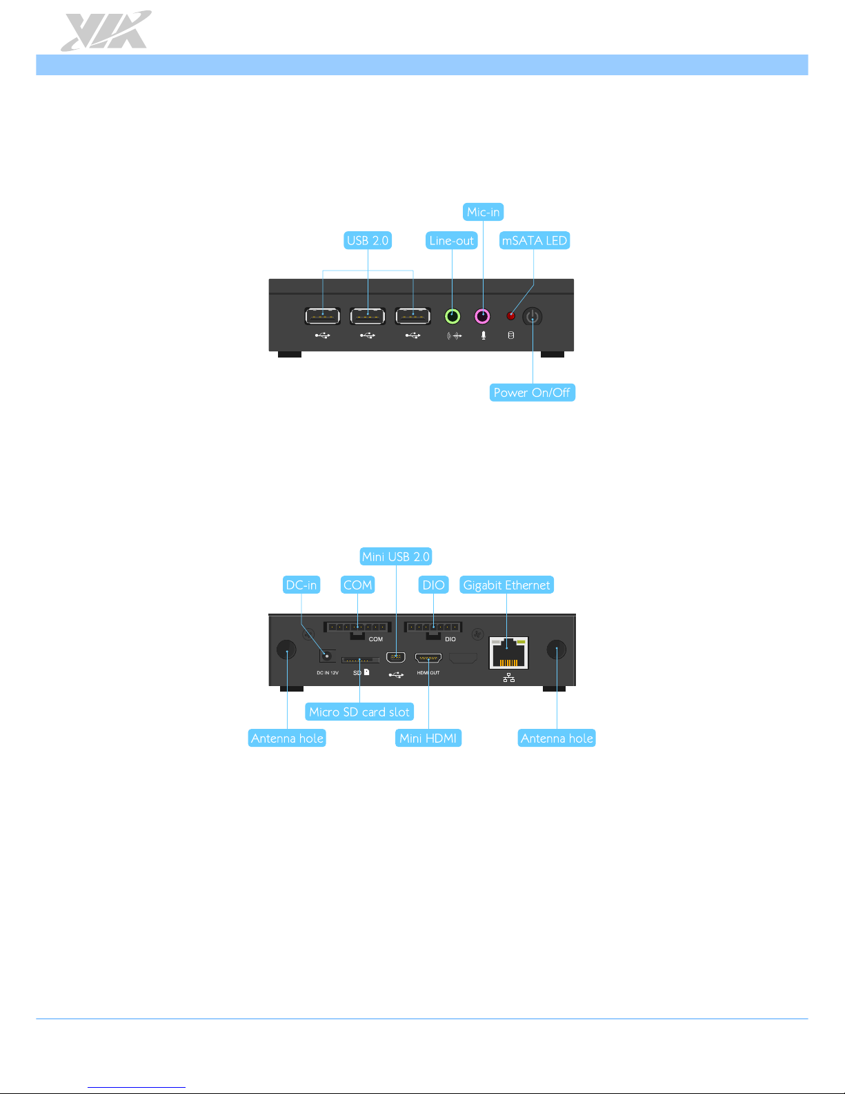
Front Panel I/O
Page 12

ARTiGO A900 User Manual
4
o 1 x Power on/off button with built-in LED
o 1 x Red LED indicator for mSATA status
o 2 x Audio jacks: Line-out and Mic-in
o 3 x USB 2.0 ports
Back Panel I/O
o 1 x 8-pin COM connector (RS-232/485)
o 1 x 7-pin DIO connector supports 4-bit GPIO (2 GPI + 2 GPO)
o 1 x Mini HDMI-out port
o 1 x Mini USB 2.0 port (Type AB connector)
o 1 x Micro SD card slot
o 1 x Gigabit Ethernet port (RJ-45)
o 1 x DC-in jack
o 2 x Antenna holes for 3G/Wi-Fi (manufacturing option)
Bottom Panel I/O (opening cover)
o 1 x miniPCIe slot
o 1 x mSATA slot
o 1 x Console debug pin header
Power Supply
o 12V DC-in (typical: 5W)
Mechanical
o
Construction
• Aluminum top cover
• Metal chassis housing
• Removable bottom access door for mSATA slot and mini PCIe slot access
o
Mounting
• Support VESA mount (100mm x 100mm) (optional)
o
Dimension (W x H x D)
• 125mm x 30mm x 125mm (4.92” x 1.18” x 4.92”)
o
Weight
• 0.525kg (1.15lbs)
Environmental Specification
o
Operating Temperature
• -5°C ~50°C
o
Operating Humidity
• 0% ~ 90% @ 45°C (non- condensing)
o
Vibration Loading During Operation (with onboard eMMC and mSATA)
• 5Grms, IEC 60068-2-64, random, 5~500Hz, 1hr/axis
o
Shock During Operation (with onboard eMMC and mSATA)
• 50G, IEC 60068-2-27, half size, 11ms duration
o
Compliance
• CE, FCC, CCC Class A
Page 13
ARTiGO A900 User Manual
5
Software Compatibility (Operating System)
o Android 4.4.2
Note:
As the operating temperature provided in the specifications is a result of the test performed in VIA’s chamber, a
number of variables can influence this result. Please note that the working temperature may vary depending on
the actual situation and environment. It is highly suggested to execute a solid testing and take all the variables
into consideration when building the system. Please ensure that the system runs well under the operating
temperature in terms of application.
Page 14
ARTiGO A900 User Manual
6
1.3. Panel Layout
Figure 1: Front panel I/O layout
Figure 2: Back panel I/O layout
Page 15

ARTiGO A900 User Manual
7
1.4. Dimensions
Figure 3: Front side view dimensions
Figure 4: Right side view dimension
Figure 5: Bottom side view dimensions
Page 16

ARTiGO A900 User Manual
8
2. External I/O Pin Descriptions and
Functionality
This chapter provides information about the ARTiGO A900’s external I/O ports, LED indicator and their
functionality.
2.1. Power On/Off Button
The ARTiGO A900 comes with a Power button with built-in power LED indicator. The Power button can
support three modes:
System Suspend/Resume
(press the button once),
Popup power control menu
(press
the button for 4 seconds) and
System Off
(press the button for 8 seconds).
Figure 6: Power on/off button diagram
2.2. LED Indicator
There is one LED on the front panel of the ARTiGO A900 that indicates the status of the system:
• mSATA LED flashes in red and indicates the mSATA storage activity.
Figure 7: LED indicator diagram
2.3. Audio Jacks
The ARTiGO A900 offers High Definition Audio through 3.5 mm TRS jack connectors on the front panel:
Line-out and Mic-in.
The Line-out jack is for connecting to external speakers or headphones. The Mic-in jack is for connecting to a
microphone.
Figure 8: Audio jack diagram
Page 17

ARTiGO A900 User Manual
9
Jack Description
Line-out TRS jack, 3.5mm Ø 5P, 90 Degree, Female, shielded
Mic-in TRS jack, 3.5mm Ø 5P, 90 Degree, Female, shielded
Table 1: Audio jack description
Page 18

ARTiGO A900 User Manual
10
2.4. USB 2.0 Port
The ARTiGO A900 is equipped with three USB 2.0 ports on the front panel. Each USB port gives complete
Plug and Play and hot swap capability for external devices. The USB interface complies with USB UHCI, Rev.
2.0. The pinout of the USB 2.0 ports are shown below.
Figure 9: USB 2.0 port diagram
USB1
USB2
USB3
Pin Signal Pin Signal
Pin Signal
1 VCC 1 VCC 1 VCC
2 USB1 data- 2 USB2 data- 2 USB3 data-
3 USB1 data+ 3 USB2 data+ 3 USB3 data+
4 GND 4 GND 4 GND
Table 2: USB 2.0 ports pinout
2.5. Gigabit Ethernet Port
The ARTiGO A900 is equipped with a Gigabit Ethernet port. The Gigabit Ethernet port is using 8 Position 8
Contact (8P8C) receptacle connector or commonly referred to as RJ-45. It is fully compliant with IEEE 802.3
(10BASE-T), 802.3u (100BASE-TX), and 802.3ab (1000BASE-T) standards. The pinout of the Gigabit Ethernet
port is shown below.
Figure 10: Gigabit Ethernet port diagram
Pin Signal
1 LAN1_TD0+
2 LAN1_TD0-
3 LAN1_TD1+
4 LAN1_TD1-
5 LAN1_TD2+
6 LAN1_TD2-
7 LAN1_TD3+
8 LAN1_TD3-
Table 3: Gigabit Ethernet port pinout
Page 19

ARTiGO A900 User Manual
11
The Gigabit Ethernet port (RJ-45) has two LED indicators on the front side to show its Active/Link status and
Speed status.
Left LED Right LED
Link Off Off Off
Speed_10Mbit The LED is On in Green color (flash)
Off
Speed_100Mbit The LED is On in Red color (flash) Off
Speed_1000Mbit Off The LED is On in Orange color (flash)
Table 4: Gigabit Ethernet port LED color definition
2.6. Mini HDMI-Out Port
The ARTiGO A900 is equipped with mini HDMI-out port (19-pin HDMI® Type C connector) located on the
back panel. The HDMI-out port is used to connect high definition video and digital audio using a single cable.
It allows connecting the digital video devices which utilize a high definition video signal. The pinout of the
HDMI-out port is shown below.
Figure 11: Mini HDMI-out port diagram
Pin Signal
1 TMDS Data2 Shield
2 TMDS Data2+
3 TMDS Data2-
4 TMDS Data1 Shield
5 TMDS Data1+
6 TMDS Data1-
7 TMDS Data0 Shield
8 TMDS Data0+
9 TMDS Data0-
10 TMDS Clock Shield
11 TMDS Clock+
12 TMDS Clock-
13 DDC/CEC Ground
14 CEC
15 SCL
16 SDA
17 Reserved
18 +5V Power
19 Hot Plug Detect
Table 5: Mini HDMI-out port pinout
2.7. Mini USB 2.0 Port
Page 20

ARTiGO A900 User Manual
12
The ARTiGO A900 has a Mini USB 2.0 port located on the back panel. The Mini USB 2.0 interface port gives
complete Plug and Play and hot swap capability for external devices and it complies with USB UHCI, rev. 2.0.
The Mini USB 2.0 port uses the USB Type AB receptacle connector. The pinout of the Mini USB port is shown
below.
Figure 12: Mini USB 2.0 port diagram
Pin Signal
1 VCC (+5V)
2 USBH1-
3 USBH1+
4 ID (GND)
5 GND
Table 6: Mini USB 2.0 port pinout
Page 21

ARTiGO A900 User Manual
13
2.8. Micro SD Card Slot
The ARTiGO A900 comes with a Micro SD card slot located on the back panel. The Micro SD card slot
enables storage of Micro SD card memory up to 32GB capacity.
Figure 13: Micro SD card slot diagram
Pin Signal
1 SD0DATA2
2 SD0DATA3
3 SD0CMD
4 VDD (3.3V)
5 SD0CLK
6 GND
7 SD0DATA0
8 SD0DATA1
9 SD0_CD
Table 7: Micro SD card slot pinout
2.9. DIO Connector
The ARTiGO A900 is equipped with Digital I/O connector (7-pin), which offers Digital I/O communication
interface to support two GPI and two GPO signals. The pinout of the Digital I/O connector is shown below.
Figure 14: DIO connector diagram
Pin Signal
1 GPIO5
2 GPIO7
3 GPIO6
4 GPIO8
5 GND
6 DIO_PW (+12V/+5V)
7 COM_PW (+12V/+5V)
Table 8: DIO connector pinout
Page 22

ARTiGO A900 User Manual
14
2.10. COM Connector
The ARTiGO A900 provides one COM connector (8-pin) for serial communications. The COM connector can
be configured as RS-232 or RS-485 mode through onboard jumper settings and it can support +5V or +12V.
See page 19 for details on setting the voltage. The pinout of the COM connector is shown below.
Figure 15: COM connector diagram
Pin
Signal
1 DCD1
2 SIN1(Rx)
3 SOUT1(Tx)
4 DTR1
5 GND
6 DSR1
7 RTS1
8 CTS1
Table 9: COM connector pinout
2.11. DC-In Jack
The ARTiGO A900 comes with a DC power input jack on the back panel that carries +12V DC external
power input. The pinout of the DC-in jack is shown below.
Figure 16: DC-in jack diagram
Pin
Signal
1 +12V
2 GND
Table 10: DC-in jack pinout
Page 23

ARTiGO A900 User Manual
15
3. Onboard I/O
This chapter provides information about the onboard slots and pin header.
3.1. mSATA Slot
The ARTiGO A900 comes with mSATA slot to support mSATA flash drive module to have flexible storage.
The mSATA slot is labeled as “MSATA”. The location of the mSATA slot is shown below.
Figure 17: mSATA slot diagram
3.2. MiniPCIe Slot
The ARTiGO A900 is equipped with miniPCIe slot for wireless networking option such as 3G and Wi-Fi
modules. The MiniPCIe slot is compatible with miniPCIe 2.0 modules that has full-length or half length in size.
The location of the miniPCIe slot is shown below.
Figure 18: MiniPCIe slot diagram
Page 24

ARTiGO A900 User Manual
16
3.3. Console Debug Pin Header
The ARTiGO A900 is equipped with Console debug pin header used for debugging the console using the
Console cable. The Console debug pin header is labeled as “CONSOLE”. The location of the Console debug
pin header is shown below.
Figure 19: Console pin header diagram
Page 25

ARTiGO A900 User Manual
17
4. Onboard Jumpers
This section will explain how to configure the ARTiGO A900 to match the needs of your application by
setting the jumpers.
Jumper Description
A jumper consists of pair conductive pins used to close in or bypass an electronic circuit to set up or
configure particular feature using a jumper cap. The jumper cap is a small metal clip covered by plastic. It
performs like a connecting bridge to short (connect) the pair of pins. The usual colors of the jumper cap are
black/red/blue/white/yellow.
Basic Jumper Configuration
There are two settings of the jumper pin: “
Short
and
Open
”. The pins are “
Short
” when a jumper cap is placed
on the pair of pins. The pins are ”
Open
” if the jumper cap is removed.
In addition, there are jumpers that have three or more pins, and some pins are arranged in series. In case of a
jumper with three pins, place the jumper cap on pin 1 and pin 2 or pin 2 and 3 to
Short
it.
Some jumper size is small or mounted on the crowded location on the board that makes it difficult to access.
Therefore, using a long-nose pliers in installing and removing the jumper cap is very helpful.
Figure 20: Jumper settings example
Caution:
Make sure to install the jumper cap on the correct pins. Installing it in the wrong pin might cause damage and
malfunction.
Page 26

ARTiGO A900 User Manual
18
4.1. COM Mode Select Jumper
The ARTiGO A900 provides a jumper that enables to select mode interface for COM connector. The COM
connector modes selections are RS-232 and RS-485. The jumper is labeled as “COM1_SET”.The jumper
settings are shown below.
Figure 21: COM mode select jumper diagram
Table 11: COM mode select jumper settings
Settings
Pin
1-2
Pin
3-4
Pin
5-6
Pin
7-8
Pin
9-10
Pin
11-12
Pin
13-14
Pin
15-16
Pin
17-18
RS-232 (Default) Open Open Open
Short
Open Open Open Open
Short
RS-485 Open
Short
Open Open
Short
Open Open Open
Short
Page 27

ARTiGO A900 User Manual
19
4.2. COM Voltage Select Jumper
The voltage for COM connector is controlled by the jumper labeled as “COM1_PW”. The jumper settings
can be Normal/No power, +5V or +12V. Normal/No power is the default setting.
Figure 22: COM voltage select jumper diagram
Setting Pin 1 Pin 2 Pin 3
Normal/No power (Default) Open Open Open
+5V Short Short Open
+12V Open Short Short
Table 12: COM voltage select jumper settings
4.3. DIO Voltage Select Jumper
The ARTiGO A900 has a DIO voltage select jumper (DIO_PW) that is used to setup the pin 6 of the DIO
connector (Refer to section 2.9. DIO Connector).
Figure 23: DIO voltage select jumper diagram
Setting Pin 1 Pin 2 Pin 3
Page 28

ARTiGO A900 User Manual
20
Normal/No power (Default) Open Open Open
+5V Short Short Open
+12V Open Short Short
Table 13: DIO voltage select jumper settings
Page 29

ARTiGO A900 User Manual
21
4.4. Miscellaneous Select Jumper
The ARTiGO A900 has a miscellaneous select jumper that is used to enable/disable the SD card write protect,
detect the active/inactive audio headphone, and auto power-on function. The jumper is labeled as “JM3”. The
jumper settings are shown below.
Figure 24: Miscellaneous select jumper diagram
SD Card Write Protect Settings Pin 1-2
Disable (Default) Short
Enable Open
Reserved Pin 3-4
(Default) Short
Open
Audio Head Phone Detect Settings Pin 5-6
Active (Default) Short
Inactive Open
USB Bus Selection Settings Pin 7-8
USB to MiniPCIe (Default) Short
USB to Wi-Fi Open
Auto Power On Function by H/W Settings Pin 9-10
Enable (Default) Short
Disable Open
Page 30

ARTiGO A900 User Manual
22
Table 14: Miscellaneous select jumper settings
Note:
In order to enable the Watchdog function, Auto Power On Function must be enabled first.
Page 31

ARTiGO A900 User Manual
23
5. Hardware Installation
This chapter provides information about hardware installation procedures. It is recommended to use a
grounded wrist strap before handling computer components. Electrostatic discharge (ESD) can damage some
components.
5.1. Installing the mSATA module
Step 1
Locate the bottom access cover of the chassis. Loosen the screw to remove the bottom access cover.
Figure 25: Removing the bottom access cover
Step 2
Align the notch on the mSATA module with the protruding wedge on the mSATA slot then insert the
module at a 30° angle.
Figure 26: Inserting mSATA module
Page 32

ARTiGO A900 User Manual
24
Step 3
Once the mSATA module has been fully inserted, push down the module until the screw hole aligns with
the standoff hole. Then secure the module with screw.
Figure 27: Securing mSATA module
Page 33

ARTiGO A900 User Manual
25
5.2. Installing the miniPCIe 3G/Wi-Fi module and antenna
Step 1
Align the notch on the miniPCIe 3G/Wi-Fi module with the protruding wedge on the miniPCIe slot then insert
the module at a 30° angle.
Figure 28: Installing miniPCIe 3G/Wi-Fi module
Step 2
Once the module has been fully inserted, push down the module until the screw holes align with the
standoff holes. Then secure the module with screw.
Figure 29: Securing miniPCIe 3G/Wi-Fi module
Step 3
Remove six screws of the top cover.
Page 34

ARTiGO A900 User Manual
26
Figure 30: Unscrewing the top cover
Page 35

ARTiGO A900 User Manual
27
Step 4
Slide the top cover horizontally to disengage it from the chassis then pull up to remove the top cover. Then
remove the antenna hole cover.
Figure 31: Removing top cover and antenna hole cover
Step 5
Insert the 3G/Wi-Fi antenna cable into the antenna hole from the inside of the chassis. Insert the washer,
fasten it with the nut, and install the external antenna. Insert the other end of the antenna cable into the
available or suitable space going down to the bottom side of the system. Stretch the cable to reach the
installed miniPCIe 3G/Wi-Fi module.
Figure 32: Installing 3G/Wi-Fi antenna
Page 36

ARTiGO A900 User Manual
28
Step 6
Gently connect the other end of the 3G/Wi-Fi antenna cable to the micro-RF connector on the miniPCIe
3G/Wi-Fi module.
Figure 33: Connecting 3G/Wi-Fi antenna cable to the miniPCIe module
Step 7
Reinstall the bottom access cover.
Figure 34: Reinstalling the bottom access cover
Page 37

ARTiGO A900 User Manual
29
5.3. Installing the Rubber feet
Step 1
Locate the designated areas for rubber feet at the bottom side of the chassis.
Step 2
Attach carefully each rubber foot. Firmly press it down to ensure the rubber foot is properly in place.
Figure 35: Installing the rubber feet
Page 38

ARTiGO A900 User Manual
30
5.4. Connecting Console cable
The Console cable is used for debugging the console
Step 1
Remove the bottom access cover to locate the Console debug pin header labeled as “CONSOLE”.
Step 2
Gently attach the Console cable to the Console debug pin header.
Figure 36: Connecting Console cable
Step 3
After debugging, remove the Console cable then reinstall the bottom access cover.
Page 39

ARTiGO A900 User Manual
31
5.5. Installing the VESA mounting kit (optional)
An optional VESA mounting kit is available for mounting the ARTiGO A900 behind the monitor.
Step 1
Attach the VESA bracket on the back of the ARTiGO A900 using four M4 x 6mm screws.
Figure 37: Installing the VESA bracket
Cautions:
1. Remove first the rubber feet before installing the VESA bracket.
2. Do not use other types of screws for VESA bracket; these might damage the internal board.
Step 2
Align the VESA mounting hole of the VESA plate to the VESA hole on the back of the monitor. Secure the
VESA mounting plate with four screws.
Page 40

ARTiGO A900 User Manual
32
Figure 38: Installing the VESA plate
Page 41

ARTiGO A900 User Manual
33
Step 3
Hook in the VESA bracket (with the ARTiGO A900 system) by sliding into the VESA plate. Then connect all
the necessary cables on the back panel of the system.
Figure 39: Installing ARTiGO A900 system to the VESA plate
Page 42

ARTiGO A900 User Manual
34
5.6. Connecting the COM and DIO cables
Step 1
Locate the COM and DIO connectors on the back panel.
Step 2
Follow the proper orientation of the connectors. Gently connect the COM and DIO cables on the COM and
DIO connectors respectively.
Figure 40: Connecting the COM and DIO cables
Page 43

ARTiGO A900 User Manual
35
6. Software and Technical Supports
6.1. Android Support
The VIA ARTiGO A900 is highly compatible with Android 4.4.2
6.1.1. Driver Installation
Support and drivers are provided through various methods including:
• Drivers provided by VIA
• Using a driver built into a distribution package
• Visiting
www.viatech.com
for the latest updated drivers
6.2. Technical Supports and Assistance
• For utilities downloads, latest documentation and new information about the ARTiGO A900, go to
http://www.viatech.com/en/systems/small-form-factor-pcs/artigo-a900
• For technical support and additional assistance, always contact your local sales representative or
board distributor, or go to
http://www.viatech.com/en/about/contact/
to fill up the form request.
• For OEM clients and system integrators developing a product for long term production, other code
and resources may also be made available. Contact VIA to submit a request.
Page 44

 Loading...